Reliability of Spring Contacts in Industrial Environments - Semikron
Reliability of Spring Contacts in Industrial Environments - Semikron
Reliability of Spring Contacts in Industrial Environments - Semikron

You also want an ePaper? Increase the reach of your titles
YUMPU automatically turns print PDFs into web optimized ePapers that Google loves.
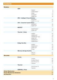
22 POWER MODULES www.semikron.com<br />
<strong>Reliability</strong> <strong>of</strong> <strong>Spr<strong>in</strong>g</strong> <strong>Contacts</strong> <strong>in</strong><br />
<strong>Industrial</strong> <strong>Environments</strong><br />
The connection between a power module substrate and a pr<strong>in</strong>ted circuit board can be established by<br />
spr<strong>in</strong>g pressure contacts. This type <strong>of</strong> contact allows easy assembly without additional solder<strong>in</strong>g. <strong>Spr<strong>in</strong>g</strong>s<br />
are used for a variety <strong>of</strong> current ranges, from sensor currents <strong>of</strong> a few milliamperes to load currents <strong>of</strong><br />
several amperes. Environmental stra<strong>in</strong>s by mechanical wear, rapid temperature changes and corrosive<br />
atmosphere are significant stress factors <strong>in</strong> <strong>in</strong>dustrial applications. The reliability <strong>of</strong> spr<strong>in</strong>g contacts under<br />
various harsh environment conditions is <strong>in</strong>vestigated. Florian Lang and Uwe Scheuermann,<br />
SEMIKRON Elektronik, Nuremberg, Germany<br />
<strong>Spr<strong>in</strong>g</strong> pressure contacts are <strong>of</strong>ten<br />
compared to the reliability <strong>of</strong> wrap- or<br />
solder-connections. However, the contact<br />
forces are <strong>in</strong> different ranges for classical<br />
wrap connectors and the spr<strong>in</strong>gs. Here,<br />
an <strong>in</strong>terconnection between a pr<strong>in</strong>ted<br />
circuit board (PCB) with driver<br />
components and power connections and<br />
a ceramic substrate (DBC) with dies is<br />
formed by spr<strong>in</strong>gs. Each spr<strong>in</strong>g has two<br />
contact spots. A loop <strong>of</strong> at least two<br />
spr<strong>in</strong>gs is used for test<strong>in</strong>g. Due to the<br />
assembly, an <strong>in</strong>dividual contact is not<br />
accessible.<br />
The pressure range determ<strong>in</strong>es the<br />
choice <strong>of</strong> contact materials for the<br />
different connectors. T<strong>in</strong> and silver plat<strong>in</strong>g<br />
are suitable for a contact force <strong>of</strong><br />
approximately 2 to 20N, while gold<br />
plat<strong>in</strong>gs are preferred <strong>in</strong> the range from 1<br />
to 2N.<br />
Frett<strong>in</strong>g corrosion<br />
‘Frett<strong>in</strong>g corrosion’ is the<br />
phenomenon <strong>of</strong> the grow<strong>in</strong>g, abrasion<br />
and compact<strong>in</strong>g <strong>of</strong> oxide particles by<br />
repeated micro-movement by vibration.<br />
This process is well known for wrap<br />
connectors <strong>of</strong> certa<strong>in</strong> contact<br />
comb<strong>in</strong>ations.<br />
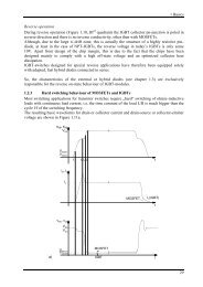
To simulate a repetitive movement <strong>of</strong><br />
the contact partners, as caused by<br />
vibration or different coefficients <strong>of</strong><br />
thermal expansion, a set-up was<br />
designed that allows a controlled<br />
movement <strong>of</strong> a PCB over a spr<strong>in</strong>g at a<br />
def<strong>in</strong>ed frequency, load and amplitude<br />
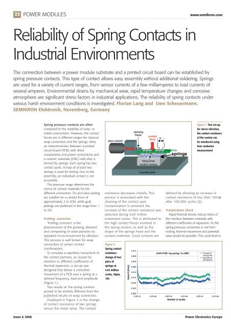
(Figure 1).<br />
Test results on the spr<strong>in</strong>g contacts<br />
proved to be entirely different from the<br />
published results on wrap connectors.<br />
Displayed <strong>in</strong> Figure 2 is the change<br />
<strong>of</strong> contact resistance <strong>of</strong> two spr<strong>in</strong>gs<br />
versus the <strong>in</strong>itial value. The contact<br />
resistance decreases <strong>in</strong>itially. This<br />
process is associated with the<br />
clean<strong>in</strong>g <strong>of</strong> the contact spot.<br />
Contam<strong>in</strong>ation is removed. No<br />
<strong>in</strong>crease <strong>of</strong> the contact resistance was<br />
detected dur<strong>in</strong>g 4.65 million<br />
movement cycles. This is attributed to<br />
the high contact forces <strong>in</strong>volved <strong>in</strong><br />
the spr<strong>in</strong>g contact, as well as the<br />
shape <strong>of</strong> the spr<strong>in</strong>gs head and the<br />
contact materials. Good contacts are<br />
Figure 2:<br />
<strong>Spr<strong>in</strong>g</strong> contact<br />
resistance<br />
change <strong>of</strong> two<br />
pairs <strong>of</strong><br />
spr<strong>in</strong>gs at<br />
4.65 million<br />
cycles, 50µm,<br />
1Hz<br />
Figure 1: Test set-up<br />
for micro-vibration,<br />
the contact resistance<br />
<strong>of</strong> the system can<br />
be monitored us<strong>in</strong>g<br />
four conductor<br />
measurement<br />
def<strong>in</strong>ed by show<strong>in</strong>g an <strong>in</strong>crease <strong>in</strong><br />
contact resistance <strong>of</strong> less than 10mΩ<br />
after 100.000 cycles [2].<br />
Temperature shock<br />
Rapid thermal shocks <strong>in</strong>duce stress <strong>of</strong><br />
the <strong>in</strong>terface between materials with<br />
different coefficients <strong>of</strong> expansion. As the<br />
spr<strong>in</strong>g pressure connection is not form<br />
lock<strong>in</strong>g, thermal movement and potential<br />
wear would be possible. This could lead to<br />
Issue 6 2006<br />
Power Electronics Europe
24 POWER MODULES www.semikron.com<br />
a change <strong>of</strong> the contact force, orientation<br />
and <strong>in</strong>terface.<br />
To evaluate the development <strong>of</strong> the<br />
contact resistance the change <strong>of</strong> the<br />
resistance aga<strong>in</strong>st the first full cycle is<br />
plotted. The temperature evolution <strong>of</strong> each<br />
cycle was measured by a soldered<br />
thermocouple attached to the device under<br />
test (DUT).<br />
It was found that some contact<br />
systems were susceptible to degradation<br />
<strong>of</strong> the contact resistance: As an example<br />
a test system with nickel DBC shows a<br />
rise <strong>of</strong> the contact resistance due to<br />
oxidation.<br />
Experiments were performed to verify<br />
the beneficial effect <strong>of</strong> higher currents on<br />
the contact resistance. In literature a<br />
change <strong>of</strong> the contact resistance is <strong>of</strong>ten<br />
attributed to th<strong>in</strong> surface layers [2]. ‘Drycircuit<br />
conditions’ accord<strong>in</strong>g to DIN EN<br />
60512-2-1 are limited to a current <strong>of</strong> up to<br />
100mA and a voltage <strong>of</strong> up to 20mV to<br />
avoid melt<strong>in</strong>g and dielectric breakdown,<br />
respectively.<br />
A test system was prepared with a<br />
material comb<strong>in</strong>ation that shows a gradual<br />
<strong>in</strong>crease <strong>in</strong> contact resistance over time.<br />
The current was <strong>in</strong>creased <strong>in</strong> steps from 1<br />
to 400mA. Figure 3 shows the contact<br />
resistance development. Each step leads to<br />
Figure 3: Test<br />
System:<br />
Influence <strong>of</strong><br />
the current<br />
level on the<br />
contact<br />
resistance <strong>of</strong><br />
an aged<br />
contact<br />
system us<strong>in</strong>g<br />
a copper DBC<br />
Figure 4:<br />
M<strong>in</strong>iSKiiP II<br />
contact<br />
system -<br />
temperature<br />
shock test<br />
us<strong>in</strong>g<br />
an ENIG DBC<br />
at a<br />
permanent<br />
current <strong>of</strong><br />
1mA<br />
a significant reduction <strong>of</strong> the contact<br />
resistance. Test<strong>in</strong>g performed at higher<br />
permanent current levels confirms these<br />
results. Practically no changes <strong>in</strong> contact<br />
resistance could be found at 6A over 200<br />
cycles. The reliability <strong>of</strong> spr<strong>in</strong>gs for load<br />
contacts is thus proven.<br />
Low current levels are typical for sensor<br />
applications. The contact resistance<br />
development <strong>of</strong> a genu<strong>in</strong>e power module<br />
is displayed <strong>in</strong> Figure 4. The optimised<br />
material selection leads to a stable contact<br />
resistance. 100 cycles with extreme<br />
temperature sw<strong>in</strong>gs are considered the<br />
Figure 5:<br />
Temperature<br />
record<strong>in</strong>g us<strong>in</strong>g a<br />
soldered<br />
thermocouple<br />
(blue l<strong>in</strong>e) and a<br />
temperature<br />
sensor connected<br />
via two spr<strong>in</strong>gs<br />
(red l<strong>in</strong>e)<br />
<strong>in</strong>dustrial lifetime requirement. The largest<br />
change <strong>in</strong> contact resistance across a daisy<br />
cha<strong>in</strong> <strong>of</strong> eight spr<strong>in</strong>gs is measured to be<br />
only 100mΩ, even after 200 temperature<br />
cycles.<br />
An extended temperature cycl<strong>in</strong>g test<br />
shows the temperature measured via a<br />
temperature sensor connected by spr<strong>in</strong>gs<br />
and a thermocouple. Figure 5 displays the<br />
temperature measurement for selected<br />
cycles. The temperature evolution <strong>of</strong> the<br />
thermocouple and the temperature sensor<br />
show a slightly different gradient, due to<br />
the differences <strong>in</strong> thermal capacity. The<br />
temperature sensor signal was stable for<br />
2000 cycles; for the extreme changes <strong>in</strong><br />
temperature this is equivalent to 20 times<br />
the <strong>in</strong>dustrial lifetime requirement <strong>of</strong> a<br />
power module. The soldered connection <strong>of</strong><br />
the reference thermocouple failed at 1000<br />
cycles and had to be replaced (see arrow<br />
<strong>in</strong> Figure 5).<br />
Corrosive atmosphere<br />
Corrosive atmosphere test<strong>in</strong>g<br />
<strong>in</strong>vestigates the contact reliability <strong>in</strong> an<br />
<strong>in</strong>dustrial environment. Due to the high<br />
contact forces <strong>of</strong> the spr<strong>in</strong>gs, the metallic<br />
contact partners are impervious to outside<br />
contam<strong>in</strong>ation. Corrosion products could<br />
not be detected by EDX analysis <strong>in</strong>side the<br />
contact area. Test<strong>in</strong>g was evaluated by<br />
measur<strong>in</strong>g contact resistance before and<br />
after the test. The change <strong>in</strong> contact<br />
resistance for various systems was<br />
negligible. No signs <strong>of</strong> electromigration<br />
could be found <strong>in</strong> a test with additionally<br />
applied bias.<br />
Intermetallic phases<br />
T<strong>in</strong> on copper plat<strong>in</strong>g is known to grow<br />
<strong>in</strong>to <strong>in</strong>termetallic phases with changed<br />
mechanical properties. Those <strong>in</strong>termetallic<br />
phases can impair solder<strong>in</strong>g due to the<br />
formation <strong>of</strong> oxide layers that are difficult to<br />
remove with normal fluxes.<br />
The growth <strong>of</strong> <strong>in</strong>termetallic phases is<br />
based on a diffusion process, and thus<br />
dependent on temperature. The pressure<br />
Issue 6 2006<br />
Power Electronics Europe