Hard switching behaviour of MOSFETs and IGBTs - Server ...
Hard switching behaviour of MOSFETs and IGBTs - Server ...
Hard switching behaviour of MOSFETs and IGBTs - Server ...

You also want an ePaper? Increase the reach of your titles
YUMPU automatically turns print PDFs into web optimized ePapers that Google loves.
1 Basics<br />
Reverse operation<br />
During reverse operation (Figure 1.10, III rd quadrant) the IGBT collector pn-junction is poled in<br />
reverse direction <strong>and</strong> there is no inverse conductivity, other than with <strong>MOSFETs</strong>.<br />
Although, due to the large n - -drift zone, this is actually the structure <strong>of</strong> a highly resistive pindiode,<br />
at least in the case <strong>of</strong> NPT-<strong>IGBTs</strong>, the reverse voltage in today’s <strong>IGBTs</strong> is only some<br />
10V. Apart from design <strong>of</strong> the chip margin, this is due to the fact that the chips have been<br />
designed mainly to comply with a high <strong>of</strong>f-state voltage <strong>and</strong> an optimized collector heat<br />
dissipation.<br />
IGBT-switches designed for special reverse applications have therefore been equipped solely<br />
with adapted, fast hybrid diodes connected in series.<br />
So, the characteristics <strong>of</strong> the external or hybrid diodes (see chapter 1.3) are exclusively<br />
responsible for the reverse on-state <strong>behaviour</strong> <strong>of</strong> IGBT-modules.<br />
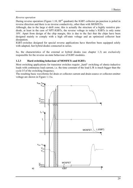
1.2.3 <strong>Hard</strong> <strong>switching</strong> <strong>behaviour</strong> <strong>of</strong> <strong>MOSFETs</strong> <strong>and</strong> <strong>IGBTs</strong><br />
Most <strong>switching</strong> applications for transistor switches require „hard“ <strong>switching</strong> <strong>of</strong> ohmic-inductive<br />
loads with continuous load current, i.e. the time constant <strong>of</strong> the load L/R is much bigger than the<br />
cycle l/f <strong>of</strong> the <strong>switching</strong> frequency.<br />
The resulting basic waveforms for drain or collector current <strong>and</strong> drain-source or collector-emitter<br />
voltage are shown in Figure 1.11a.<br />
V GG<br />
V GS(th)<br />
V GE(th)<br />
t 1 t 2 t 3 t 4<br />
t<br />
i D<br />
, i C<br />
I L<br />
MOSFET<br />
I t<br />
(IGBT)<br />
t<br />
v DS<br />
, v CE<br />
V DD<br />
V CC<br />
V DS(on) VCE(sat)<br />
MOSFET<br />
a) IGBT<br />
t<br />
29
1 Basics<br />
V DD<br />
I L<br />
i D<br />
, i C<br />
on<br />
I L<br />
V GG<br />
i D<br />
<strong>of</strong>f<br />
V CC<br />
I L<br />
V DD<br />
V CC<br />
v DS<br />
, v CE<br />
V GG<br />
i C<br />
b)<br />
Figure 1.11<br />
Typical “hard” <strong>switching</strong> <strong>behaviour</strong> <strong>of</strong> MOSFET <strong>and</strong> IGBT (ohmic-inductive load with<br />
free-wheeling circuit)<br />
a) Current <strong>and</strong> voltage waveforms<br />
b) Curve <strong>and</strong> measurement circuit<br />
As already depicted in chapter 0, Figure 0.4 a high short-time transistor current <strong>and</strong> voltage<br />
during turn-on <strong>and</strong> turn-<strong>of</strong>f are typical features <strong>of</strong> „hard <strong>switching</strong>“.<br />
In contrast to all types <strong>of</strong> thyristors, such transistors operate without passive snubber networks<br />
thanks to the „dynamic“ junction which is generated in the drift zone during <strong>switching</strong> operation.<br />
In a transistor, however, considerable <strong>switching</strong> energy<br />
E<br />
on<br />
, E<br />
<strong>of</strong>f<br />
=<br />
∫ u ⋅idt<br />
t on , t <strong>of</strong>f<br />
is dissipated as explained by the graph i C = f(v CE ) (<strong>and</strong> i D = f(v DS )) in Figure 1.11b.<br />
The curve may be directed nearer towards the axes with passive snubber networks. Switching<br />
losses are „shifted“ from the transistor to the snubber, the total efficiency will decrease in most<br />
cases (chapter 3.8).<br />
Since the size <strong>of</strong> the operating area is influenced by many (non-ideal) transistor features apart<br />
from current/ voltage limitations <strong>and</strong> <strong>switching</strong> times, the SOA (Safe Operating Area) is given in<br />
the datasheets for different operating conditions (see chapters 2.1.2, 2.2.3 <strong>and</strong> 2.3.3).<br />
Moreover, passive circuit elements have a tremendous influence on <strong>switching</strong> losses <strong>and</strong><br />
operating areas, apart from the non-ideal transistor features <strong>and</strong> the diode characteristics<br />
described in chapter 1.3. The effects <strong>of</strong> such passive circuit elements also indicated in Figure<br />
1.11a are explained in detail in chapter 3.4.1.<br />
Physically, the typical current-voltage characteristics in Figure 1.11a are caused by the freewheeling<br />
diode, which has to prevent current snap-<strong>of</strong>f by load inductance:<br />
30
1 Basics<br />
- When the transistor is turned on, the free-wheeling diode can only take up reverse recovery<br />
voltage (turn <strong>of</strong>f), after the load current has completely commutated to the transistor.<br />
Therefore, the collector or drain-current has to reach the load current level, before the<br />
collector-emitter (or drain-source) voltage may fall to the on-state value.<br />
- When the transistor is turned <strong>of</strong>f, the free-wheeling diode can only take up the load current<br />
(turn on), after it has reached on-state voltage polarity. This will be the case when the<br />
collector-emitter (or drain-source) voltage has exceeded the commutation voltage level,<br />
before the collector or drain-current may fall to the cut-<strong>of</strong>f current value.<br />
As shown in Figure 1.11a, the drain-source or collector-emitter voltage <strong>of</strong> comparable<br />
components will, shortly after turn-on <strong>of</strong> the MOSFET or IGBT, drop within some 10ns to a<br />
value, that is equivalent to the voltage drop over the n - -drift area. Whereas in the MOSFET the<br />
on-state voltage has already been reached by this, the n - -area <strong>of</strong> the IGBT is now flooded with<br />
positive charge carriers from the p-collector zone. After this procedure has been finished (appr.<br />
100ns up to some µs), the static value <strong>of</strong> the on-state saturation voltage V CE(sat) , which is<br />
relatively low for highly blocking components, has been reached (conductivity modulation).<br />
During turn-<strong>of</strong>f <strong>of</strong> the MOSFET, the internal capacitances have to be recharged, that there are no<br />
charge carrier influence left in the channel area. Thereafter, the neutrality interferences in this<br />
area will quickly be reduced <strong>and</strong> the drain current will drop rapidly.<br />
The procedure within the IGBT is principally the same. However, after the emitter current in the<br />
n - -drift zone has been turned <strong>of</strong>f, a large number <strong>of</strong> p-charge carriers generated by injection from<br />
the IGBT-collector zone is still left. These p-charge carriers have now to be recombined or<br />
reduced by re-injection, which would cause a so-called collector tail current I t . (Figure 1.11a).<br />
Since this tail current will fade away within some µs only with already increased collectoremitter<br />
voltage, the hard turn-<strong>of</strong>f power losses in the IGBT are mainly determined by the tail<br />
current waveform (see chapter 2.3.2, 3.1.3) <strong>and</strong> are considerably higher than those in <strong>MOSFETs</strong>.<br />
Apart from the explained differences, the <strong>switching</strong> <strong>behaviour</strong> <strong>of</strong> <strong>MOSFETs</strong> is very similar to<br />
that <strong>of</strong> <strong>IGBTs</strong> due to the equivalent gate structure.<br />
As described in chapter 1.2.1, the forward on-state <strong>and</strong> forward <strong>of</strong>f-state capability, the reverse<br />
<strong>behaviour</strong> <strong>and</strong> the limits <strong>of</strong> the transient currents <strong>and</strong> voltages during <strong>switching</strong> are influenced by<br />
the internal structures <strong>of</strong> the bipolar transistor <strong>and</strong> the lateral resistances.<br />
The <strong>switching</strong> <strong>behaviour</strong> (<strong>switching</strong> velocity, <strong>switching</strong> losses) <strong>of</strong> MOSFET <strong>and</strong> IGBTpower<br />
modules is determined by their structural, internal capacitances (charges) <strong>and</strong> the internal <strong>and</strong><br />
outer resistances.<br />
Contrary to the ideal <strong>of</strong> a powerless voltage control via the MOSFET or IGBTgate, a frequencydependent<br />
control power is required resulting from the necessary recharge currents <strong>of</strong> the<br />
internal capacitances, see chapter 3.5.<br />
Moreover, the commutation processes are affected by the parasitic connection inductances<br />
existing in the power layout <strong>and</strong> generated by connection <strong>of</strong> transistor chips in power modules;<br />
they induce transient overvoltages <strong>and</strong> may cause oscillations due to the circuit <strong>and</strong> transistor<br />
capacitances (see chapter 3.4).<br />
In the following, the <strong>switching</strong> <strong>behaviour</strong> <strong>of</strong> <strong>MOSFETs</strong> <strong>and</strong> <strong>IGBTs</strong> is to be analysed in relation<br />
to the internal capacitances <strong>and</strong> resistances <strong>of</strong> the transistor.<br />
31
1 Basics<br />
When the MOSFET (IGBT) is turned <strong>of</strong>f, C GD (C GC ) is low <strong>and</strong> is approximately equal to C DS<br />
(C CE ).<br />
During on-state C GD (C GC ) will increase rapidly due to inversion in the enhancement layer below<br />
the gate zones, as soon as the gate-source (emitter) voltage has exceeded the drain-source<br />
(collector-emitter) voltage.<br />
Additionally, C GD (G GC ) will increase dynamically during the <strong>switching</strong> procedure due to the<br />
Millereffect:<br />
C GDdyn = C GD ( 1- dv DS /dv GS ) (MOSFET)<br />
C GCdyn = C GE ( 1- dv CE /dv GE ) (IGBT)<br />
In most datasheets the following voltage-dependent low-signal capacitances <strong>of</strong> turned <strong>of</strong>f<br />
transistors are given (see chapters 2.2.2, 2.2.3).<br />
Power MOSFET<br />
IGBT<br />
C iss = C GS + C GD C iss = C GE + C GC Input capacitance<br />
C rss = C GD C rss = C GC Reverse transfer capacitance<br />
C oss = C GD + C DS C oss = C GC + C CE Output capacitance<br />
For calculation <strong>of</strong> the <strong>switching</strong> <strong>behaviour</strong>, these datas may only be applied to a certain extent,<br />
since e.g. C iss <strong>and</strong> C rss will again increase enormously in a fully switched on transistor<br />
(V DS < V GS bzw. V CE < V GE ), a fact that is not considered in most datasheets (Figure 1.12 <strong>and</strong><br />
Figure 1.13) [277].<br />
Therefore, <strong>switching</strong> times in relation to gate current, drain-source voltage <strong>and</strong> drain current are<br />
determined with the aid <strong>of</strong> the MOSFET “gate charge characteristic” indicated in the datasheets,<br />
plotting the gate-source voltage over the gate charge Q G on condition <strong>of</strong> “rated current” <strong>and</strong><br />
20 % or 80 % <strong>of</strong> the maximum drain-source voltage (Figure 1.12).<br />
Load conditions <strong>and</strong> measurement circuit are equivalent to Figure 1.11. However, for<br />
simplification purposes, constant current is supposed to be fed to the gate.<br />
Now, <strong>switching</strong> intervals may be determined very simply with the following relation (see chapter<br />
3.5.1):<br />
i G = dQ G /dt<br />
32
1 Basics<br />
V GS<br />
[V] 16<br />
V DS1<br />
1 Basics<br />
current in the active region by the transconductance g fs with I D = g fs * V GS , will increase up to the<br />
value V GS1 = I D /g fs (time t 2 ).<br />
Since the free-wheeling diode can block the current only at t 2 , V DS will not drop considerably up<br />
to t 2 .<br />
At t = t 2 charge Q G2 has flown into the gate.<br />
Turn-on: <strong>switching</strong> interval t 2 ...t 3 (transistor during turn-on)<br />
When the free-wheeling diode is turned <strong>of</strong>f, V DS will drop almost to on-state value V DS(on) by<br />
time t 3 . Between t 2 <strong>and</strong> t 3 drain current <strong>and</strong> gate-source voltage are still coupled by<br />
transconductance; therefore, V GS remains constant. While V DS is decreasing, the Miller<br />
capacitance C GD is recharged by the gate current i G with the charge quantity (Q G3 -Q G2 ). By t = t 3<br />
charge Q G3 has flownflown? into the gate.<br />
Turn-on: <strong>switching</strong> interval t 3 ...t 4 (ohmic characteristic area)<br />
At t 3 the transistor is turned on, its curve has passed the pinch-<strong>of</strong>f area to enter the ohmic area.<br />
V GS <strong>and</strong> I D are no longer coupled by g fs .<br />
The charge conducted to the gate (Q Gtot -Q G3 ) at this point affects a further increase <strong>of</strong> V GS up to<br />
the gate control voltage V GG . Since the drain-source on-resistance R DS(on) depends on I D <strong>and</strong> V GS ,<br />
the on-state voltage V DS(on) = I D * R DS(on) may be adjusted to the physical minimum by the total<br />
charge quantity Q gtot conducted to the gate.<br />
The higher the drain voltage V DD (or commutation voltage), the bigger the charge Q gtot required<br />
to reach a certain gate-source voltage, see Figure 1.12.<br />
Turn-<strong>of</strong>f<br />
During turn-<strong>of</strong>f the described processes are running in reverse direction; the charge Q Gtot has to<br />
be conducted out <strong>of</strong> the gate by the control current.<br />
For approximations to determine the gate charge quantity required for turn-<strong>of</strong>f, the gate charge<br />
characteristic in Figure 1.12 may be used.<br />
The further the specific transistor application deviates from the „hard switch“-application<br />
described, the more the step-form <strong>of</strong> the gate-source voltage blurs. The intervals „decoupled“ by<br />
the free-wheeling diode during hard <strong>switching</strong> will then more or less merge into one another,<br />
which requires a more complex explanation <strong>of</strong> the <strong>switching</strong> <strong>behaviour</strong>. [278].<br />
The above-mentioned description may be applied to IGBTpower modules by analogy. The<br />
<strong>switching</strong> <strong>behaviour</strong> can be determined correspondingly by the gate charge characteristic also<br />
indicated in the datasheets.<br />
Since an IGBTgate is mostly switched between a positive <strong>and</strong> a negative gate voltage, also a<br />
certain charge quantity is required to switch the gate capacitance between 0V <strong>and</strong> V GG- .<br />
Therefore, the gate charge characteristic has to be extended as depicted in Figure 1.13. to<br />
calculate the total gate charges.<br />
34