Application Note - Semikron
Application Note - Semikron
Application Note - Semikron

You also want an ePaper? Increase the reach of your titles
YUMPU automatically turns print PDFs into web optimized ePapers that Google loves.
<strong>Application</strong> <strong>Note</strong> AN-11001<br />
<br />
<br />
Three not adjacent IGBTs are switched on<br />
(same consequences as above: shorting either<br />
upper half or lower half or the full DC-link)<br />
Four IGBTs switched on → DC+, DC- and N<br />
shorted.<br />
4. voltage is greater and current is less than 0 (V ><br />
0, I < 0):<br />
2L: T BOT ↔ D TOP<br />
3L NPC: T3/D6 ↔ D1/D2 (long commutation<br />
path)<br />
3L TNPC: T3/D2 ↔ D1<br />
Commutations and commutation paths<br />
NPC & TNPC:<br />
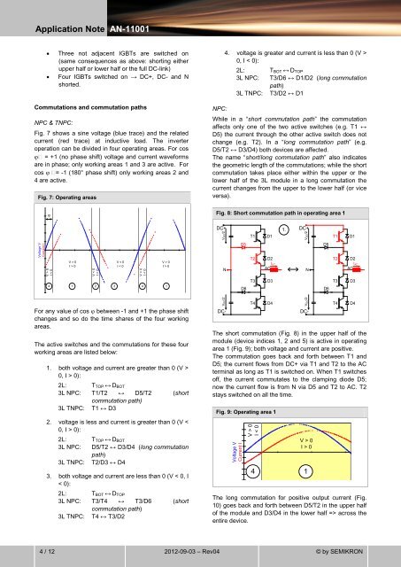
Fig. 7 shows a sine voltage (blue trace) and the related<br />
current (red trace) at inductive load. The inverter<br />
operation can be divided in four operating areas. For cos<br />
= +1 (no phase shift) voltage and current waveforms<br />
are in phase; only working areas 1 and 3 are active. For<br />
cos -1 (180° phase shift) only working areas 2 and<br />
4 are active.<br />
Fig. 7: Operating areas<br />
NPC:<br />
While in a “short commutation path” the commutation<br />
affects only one of the two active switches (e.g. T1 ↔<br />
D5) the current through the other active switch does not<br />
change (e.g. T2). In a “long commutation path” (e.g.<br />
D5/T2 ↔ D3/D4) both devices are affected.<br />
The name “short/long commutation path” also indicates<br />
the geometric length of the commutations; while the short<br />
commutation takes place either within the upper or the<br />
lower half of the 3L module in a long commutation the<br />
current changes from the upper to the lower half (or vice<br />
versa).<br />
0.9<br />
<br />
Fig. 8: Short commutation path in operating area 1<br />
DC+<br />
VDC/2<br />
T1<br />
D1<br />
1.<br />
DC+<br />
VDC/2<br />
T1<br />
D1<br />
Voltage V<br />
Current I<br />
i( t )<br />
u( t )<br />
V > 0<br />
I < 0<br />
V > 0<br />
I > 0<br />
V < 0<br />
I > 0<br />
V < 0<br />
I < 0<br />
V > 0<br />
I < 0<br />
V > 0<br />
I > 0<br />
N<br />
D5<br />
T2<br />
D2<br />
AC<br />
IAC<br />
N<br />
D5<br />
T2<br />
D2<br />
AC<br />
IAC<br />
4 1 2 3<br />
4 1<br />
D6<br />
T3<br />
D3<br />
D6<br />
T3<br />
D3<br />
0.9<br />
0 t<br />
For any value of cos between -1 and +1 the phase shift<br />
changes and so do the time shares of the four working<br />
areas.<br />
The active switches and the commutations for these four<br />
working areas are listed below:<br />
1. both voltage and current are greater than 0 (V ><br />
0, I > 0):<br />
2L: T TOP ↔ D BOT<br />
3L NPC: T1/T2 ↔ D5/T2 (short<br />
commutation path)<br />
3L TNPC: T1 ↔ D3<br />
2. voltage is less and current is greater than 0 (V <<br />
0, I > 0):<br />
2L: T TOP ↔ D BOT<br />
3L NPC: D5/T2 ↔ D3/D4 (long commutation<br />
path)<br />
3L TNPC: T2/D3 ↔ D4<br />
3. both voltage and current are less than 0 (V < 0, I<br />
< 0):<br />
2L: T BOT ↔ D TOP<br />
3L NPC: T3/T4 ↔ T3/D6 (short<br />
commutation path)<br />
3L TNPC: T4 ↔ T3/D2<br />
3<br />
VDC/2<br />
T4<br />
D4<br />
VDC/2<br />
DC-<br />
DC-<br />
The short commutation (Fig. 8) in the upper half of the<br />
module (device indices 1, 2 and 5) is active in operating<br />
area 1 (Fig. 9); both voltage and current are positive.<br />
The commutation goes back and forth between T1 and<br />
D5; the current flows from DC+ via T1 and T2 to the AC<br />
terminal as long as T1 is switched on. When T1 switches<br />
off, the current commutates to the clamping diode D5;<br />
now the current flow is from N via D5 and T2 to AC. T2<br />
stays switched on all the time.<br />
Fig. 9: Operating area 1<br />
<br />
0 .9<br />
Voltage V<br />
Current I<br />
i U( ( tx<br />
))<br />
I ( x )<br />
u ( t )<br />
0 .9<br />
0<br />
V > 0<br />
I < 0<br />
4<br />
V > 0<br />
I > 0<br />
T4<br />
D4<br />
V < 0<br />
I > 0<br />
1 2 3<br />
The long commutation for positive output current (Fig.<br />
10) goes back and forth between D5/T2 in the upper half<br />
of the module and D3/D4 in the lower half => across the<br />
entire device.<br />
4 / 12 2012-09-03 – Rev04 © by SEMIKRON