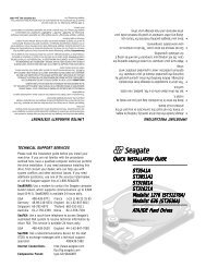
Barracuda 18LP Family: ST39175LW/LC ST318275LW ... - Seagate
Barracuda 18LP Family: ST39175LW/LC ST318275LW ... - Seagate
Barracuda 18LP Family: ST39175LW/LC ST318275LW ... - Seagate

You also want an ePaper? Increase the reach of your titles
YUMPU automatically turns print PDFs into web optimized ePapers that Google loves.
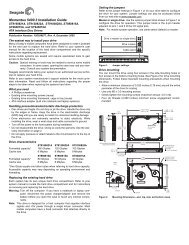
<strong>Barracuda</strong> <strong>18LP</strong> Product Manual, Rev. E 65<br />
9.7 Electrical description<br />
“<strong>LC</strong>” models use the single connection attachment (SCA) connector. This 80-pin connector is designed to plug<br />
directly into a back panel or plane. No external cables are required. Active terminators on the back panel must<br />
be provided by the user. This connector is not recommended where cabling is required.<br />
“<strong>LC</strong>” and “LW” models are Multimode drives. That is, their I/O circuits can operate as either single-ended or low<br />
voltage differential drivers/receivers (selectable using the I/O “DIFFSENS” line). They require external terminators.<br />
See Section 9.7.1 for additional information on these models.<br />
See ANSI Standard T10/1302D for detailed electrical specifications.<br />
9.7.1 Multimode—SE or LVD alternative<br />
“LW” and “<strong>LC</strong>” models have I/O circuits that can operate either in single-ended (SE) or low voltage differential<br />
mode (LVD). When the interface “DIFFSNS” line is between 0 V and .6 V, the drive interface circuits operate<br />
single-ended and up to and including 20 M transfers/s (Fast-20 or Ultra-1 SCSI). When “DIFFSNS” is between<br />
+0.7 V and +1.9 V, the drive interface circuits operate low voltage differential and up to and including 40 M<br />
transfers/sec or less (Fast-40 or Ultra-2 SCSI). This arrangement is not intended to allow dynamically changing<br />
transmission modes, but rather to prevent incompatible devices from attempting to interoperate. Multimode I/O<br />
circuits used by “<strong>LC</strong>” and “LW” devices do not operate at high voltage differential levels and should never be<br />
exposed to high voltage differential environments unless the common mode voltages in the environment are<br />
controlled to safe levels for single-ended and low voltage differential devices (see the ANSI SPI-2 specification<br />
T10/1302D).<br />
Multimode signals<br />
Multimode circuit SE alternative logic sense and signal level characteristics are described as follows:<br />
Vil (low-level input voltage) = 1.0 V maximum (signal true); minimum = Vss – 0.5 V<br />
Vih (high-level input voltage) = 1.9 V minimum (signal false); maximum = Vdd +0.5V<br />
Vihys (Input Hysteresis) = 425 mV minimum<br />
Multimode circuit LVD alternative signal characteristics are not the same as high voltage differential signals<br />
(HVD). This drive does not support HVD. The SCA-2, 80-pin connector signal/pin assignments are shown in<br />
Tables 13b and 13d, but the electrical characteristics of the signals are not the same. “<strong>LC</strong>” and “LW” model<br />
drives do not have onboard terminators. The Multimode signal lines (either SE or LVD) should be terminated<br />
with 110 ohm active terminator circuits at each end of the total cable. Termination of the I/O lines must be provided<br />
for by the Host equipment designers or end users.<br />
The SE and differential alternatives are mutually exclusive.<br />
Output characteristics<br />
Each LVD signal (V s ) driven by LVD interface drivers shall have the following output characteristics when measured<br />
at the disc drive connector (refer to figure 12):<br />
Steady state Low level output voltage* = –.95 V = < V s = < –1.55 V (signal negation/logic 0)<br />
Steady state High level output voltage* = +.95 V = < V s = < 1.55 V (signal assertion/logic 1)<br />
Differential voltage = +0.6 V minimum with common-mode voltage ranges 0.700 V = < V cm = < 1.800 V<br />
A signal that is “released” goes to the negated (false or logic 0) state because the bias of the terminator pulls<br />
the signal levels to the negated state.<br />
*These voltages shall be measured between the output terminal and the SCSI device’s logic ground reference.<br />
Refer to paragraphs 7.2.2, 8.3.2, and Annex A of ANSI SPI-3 specification, T10/1302D for details regarding<br />
LVD circuits.<br />
The output characteristics shall additionally conform to EIA RS-485.