Fireball Plus AS Product Manual - Seagate
Fireball Plus AS Product Manual - Seagate
Fireball Plus AS Product Manual - Seagate

You also want an ePaper? Increase the reach of your titles
YUMPU automatically turns print PDFs into web optimized ePapers that Google loves.
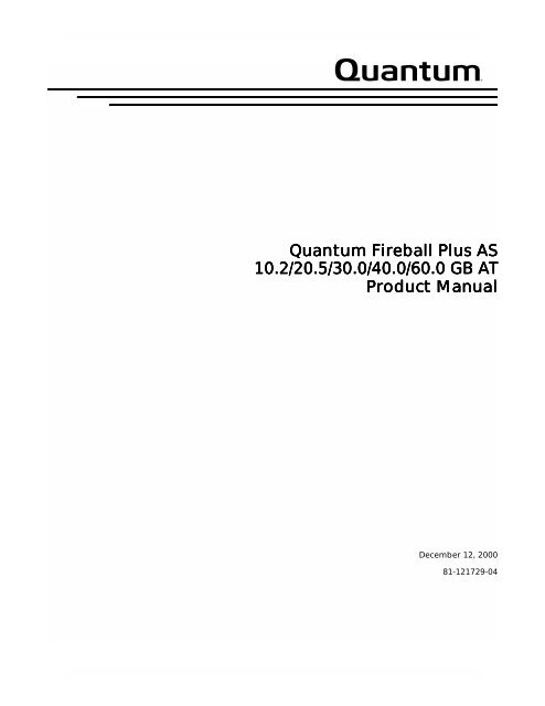
Quantum <strong>Fireball</strong> <strong>Plus</strong> <strong>AS</strong><br />
10.2/20.5/30.0/40.0/60.0 GB AT<br />
<strong>Product</strong> <strong>Manual</strong><br />
December 12, 2000<br />
81-121729-04
Quantum reserves the right to make changes and improvements to its products, without incurring<br />
any obligation to incorporate such changes or improvements into units previously sold or shipped.<br />
You can request Quantum publications from your Quantum Sales Representative or order them<br />
directly from Quantum.<br />
Publication Number: 81-121729-04<br />
UL/CSA/TUV/CE<br />
UL standard 1950 recognition granted under File No. E78016<br />
CSA standard C22.2 No. 950 certification granted under File No. LR49896<br />
TUV Rheinland EN 60 950 granted under File No. R 9677196<br />
Tested to FCC Rules for Radiated and Conducted Emissions, Part 15, Sub Part J, for Class-B<br />
Equipment.<br />
SERVICE CENTERS<br />
Quantum Service Center Quantum Asia-Pacific Pte. Ltd. Quantum Customer Service Group<br />
160 E. Tasman 50 Tagore Lane #b1-04 Quantum Ireland Ltd.<br />
San Jose, California 95134 Singapore, 2678 Finnabair Industrial Park<br />
Phone: (408) 894-4000 Phone: (65) 450-9333 Dundalk<br />
Fax: (408) 894-3218 Fax: (65) 452-2544 County Louth, Ireland<br />
http://www.quantum.com Tel: (353) 42-55350<br />
Fax: (353) 45-55355<br />
PATENTS<br />
These products are covered by or licensed under one or more of the following U.S. Patents:<br />
4,419,701; 4, 538,193 4,625,109; 4,639,798; 4,647,769; 4,647,997; 4,661,696; 4,669,004;<br />
4,675,652; 4,703,176; 4,730,321; 4,772,974; 4,783,705; 4,819,153; 4,882,671; 4,920,442;<br />
4,920,434; 4,982,296; 5,005,089; 5,027,241; 5,031,061; 5,084,791; 5,119,254; 5,160,865;<br />
5,170,229; 5,177,771; Other U.S. and Foreign Patents Pending.<br />
© 2000 Quantum Corporation. All rights reserved. Printed in U.S.A.<br />
Quantum, the Quantum logo, and AIRLOCK are trademarks of Quantum Corporation, registered<br />
in the U.S.A. and other countries. Capacity for the extraordinary, Quantum <strong>Fireball</strong> <strong>Plus</strong> <strong>AS</strong>,<br />
AutoTransfer, AutoRead, AutoWrite, DisCache, DiskWare, Defect Free Interface, and WriteCache<br />
are trademarks of Quantum Corporation. All other brand names or trademarks are the property of<br />
their manufacturers.<br />
This product or document is protected by copyright and distributed under licenses restricting its<br />
use, copying, distribution, and decompilation. No part of this product or document may be<br />
reproduced in any form by any means without prior written authorization of Quantum and its<br />
licensors, if any.<br />
RESTRICTED RIGHTS LEGEND: Use, duplication, or disclosure by the government is subject to<br />
restrictions as set forth in subparagraph (c)(1)(ii) of the Rights in Technical Data and Computer<br />
Software clause at DFARS 252.227-7013 and FAR 52.227-19.<br />
THIS PUBLICATION IS PROVIDED “<strong>AS</strong> IS’ WITHOUT WARRANTY OF ANY KIND, EITHER<br />
EXPRESS OR IMPLIED, INCLUDING, BUT NOT LIMITED TO, THE IMPLIED WARRANTIES<br />
OF MERCHANTABILITY, FITNESS FOR A PARTICULAR PURPOSE, OR NON-<br />
INFRINGEMENT.
Table of Contents<br />
Chapter 1<br />
ABOUT THIS MANUAL<br />
1.1 AUDIENCE ................................................................................................................. 1-1<br />
1.2 MANUAL ORGANIZATION..................................................................................... 1-1<br />
1.3 TERMINOLOGY AND CONVENTIONS ................................................................. 1-1<br />
1.4 REFERENCES............................................................................................................. 1-3<br />
Chapter 2<br />
GENERAL DESCRIPTION<br />
2.5 PRODUCT OVERVIEW ............................................................................................. 2-5<br />
2.6 KEY FEATURES ......................................................................................................... 2-5<br />
2.7 Regulatory Compliance Standards .............................................................................. 2-7<br />
2.8 HARDWARE REQUIREMENTS................................................................................ 2-7<br />
Chapter 3<br />
INSTALLATION<br />
3.1 SPACE REQUIREMENTS.......................................................................................... 3-1<br />
3.2 UNPACKING INSTRUCTIONS ................................................................................ 3-2<br />
3.3 HARDWARE OPTIONS............................................................................................. 3-4<br />
3.3.1 Cable Select (CS) Jumper .................................................................................. 3-5<br />
3.3.2 Drive Select (DS) Jumper .................................................................................. 3-6<br />
3.3.3 Master Jumper configuration ............................................................................. 3-6<br />
3.3.4 Jumper Parking (PK) Position ........................................................................... 3-6<br />
3.3.5 Alternate Capacity (AC) .................................................................................... 3-7<br />
3.4 ATA BUS ADAPTER.................................................................................................. 3-8<br />
3.4.1 40-Pin ATA Bus Connector ............................................................................... 3-8<br />
3.4.2 Adapter Board .................................................................................................... 3-8<br />
3.5 MOUNTING ............................................................................................................... 3-9<br />
3.5.1 Orientation ......................................................................................................... 3-9<br />
3.5.2 Clearance .......................................................................................................... 3-11<br />
3.5.3 Ventilation ........................................................................................................ 3-11<br />
3.6 COMBINATION CONNECTOR (J1) ...................................................................... 3-11<br />
3.6.1 DC Power (J1, Section A) ................................................................................ 3-12<br />
3.6.2 External Drive Activity LED ............................................................................ 3-12<br />
3.6.3 ATA Bus Interface Connector (J1, Section C) ................................................ 3-12<br />
3.7 FOR SYSTEMS WITH A MOTHERBOARD ATA ADAPTER............................... 3-13<br />
3.8 FOR SYSTEMS WITH AN ATA ADAPTER BOARD............................................. 3-13<br />
3.8.1 Adapter Board Installation ............................................................................... 3-13<br />
3.9 TECHNIQUES IN DRIVE CONFIGURATION ...................................................... 3-15<br />
3.9.1 The 528-Megabytes Barrier .............................................................................. 3-15<br />
Quantum <strong>Fireball</strong> <strong>Plus</strong> <strong>AS</strong> 10.2/20.5/30.0/40.0/60.0 GB AT<br />
iii
Table of Contents<br />
3.9.2 The 8.4-Gigabytes Barrier ................................................................................. 3-16<br />
3.9.3 Operating system limitations ............................................................................ 3-16<br />
3.10 SYSTEM STARTUP AND OPERATION ................................................................. 3-17<br />
Chapter 4<br />
SPECIFICATIONS<br />
4.1 SPECIFICATION SUMMARY ................................................................................... 4-1<br />
4.2 FORMATTED CAPACITY.......................................................................................... 4-3<br />
4.3 DATA TRANSFER RATES......................................................................................... 4-3<br />
4.4 TIMING SPECIFICATIONS ...................................................................................... 4-4<br />
4.5 POWER ........................................................................................................................ 4-5<br />
4.5.1 Power Sequencing .............................................................................................. 4-5<br />
4.5.2 Power Reset Limits ............................................................................................. 4-5<br />
4.5.3 Power Requirements ........................................................................................... 4-6<br />
4.6 ACOUSTICS................................................................................................................ 4-7<br />
4.7 MECHANICAL ........................................................................................................... 4-8<br />
4.8 ENVIRONMENTAL CONDITIONS .......................................................................... 4-8<br />
4.9 SHOCK AND VIBRATION........................................................................................ 4-9<br />
4.10 HANDLING the DRIVE ........................................................................................... 4-10<br />
4.11 RELIABILITY............................................................................................................ 4-10<br />
4.12 ELECTROMAGNETIC SUSCEPTIBILITY.............................................................. 4-11<br />
4.13 SPINDLE IMBALANCE ........................................................................................... 4-11<br />
4.14 DISK ERRORS .......................................................................................................... 4-11<br />
Chapter 5<br />
B<strong>AS</strong>IC PRINCIPLES OF OPERATION<br />
5.1 Quantum <strong>Fireball</strong> <strong>Plus</strong> <strong>AS</strong> DRIVE MECHANISM..................................................... 5-1<br />
5.1.1 Base Casting Assembly ....................................................................................... 5-3<br />
5.1.2 DC Motor Assembly ........................................................................................... 5-3<br />
5.1.3 Disk Stack Assemblies ........................................................................................ 5-3<br />
5.1.4 Headstack Assembly ........................................................................................... 5-4<br />
5.1.5 Rotary Positioner Assembly ................................................................................ 5-4<br />
5.1.6 Automatic Actuator Lock ................................................................................... 5-4<br />
5.1.7 Air Filtration ....................................................................................................... 5-5<br />
5.2 DRIVE ELECTRONICS .............................................................................................. 5-5<br />
5.2.1 Integrated µProcessor, Disk Controller and ATA Interface Electronics ............ 5-6<br />
5.2.2 Read/Write <strong>AS</strong>IC ................................................................................................ 5-8<br />
5.2.3 PreAmplifier and Write Driver ......................................................................... 5-10<br />
5.3 FIRMWARE FEATURES .......................................................................................... 5-10<br />
5.3.1 Disk Caching ..................................................................................................... 5-10<br />
5.3.2 Head and Cylinder Skewing ............................................................................. 5-12<br />
5.3.3 Error Detection and Correction ........................................................................ 5-13<br />
5.3.4 Defect Management .......................................................................................... 5-15<br />
iv<br />
Quantum <strong>Fireball</strong> <strong>Plus</strong> <strong>AS</strong> 10.2/20.5/30.0/40.0/60.0 GB AT
Table of Contents<br />
Chapter 6<br />
ATA BUS INTERFACE AND ATA COMMANDS 6-1<br />
6.1 INTRODUCTION ....................................................................................................... 6-1<br />
6.2 SOFTWARE INTERFACE.......................................................................................... 6-1<br />
6.3 MECHANICAL DESCRIPTION ................................................................................ 6-1<br />
6.3.1 Drive Cable and Connector ................................................................................ 6-1<br />
6.4 ELECTRICAL INTERFACE ....................................................................................... 6-1<br />
6.4.1 ATA Bus Interface .............................................................................................. 6-1<br />
6.4.2 Host Interface Timing ........................................................................................ 6-9<br />
6.5 REGISTER ADDRESS DECODING ....................................................................... 6-21<br />
6.6 REGISTER DESCRIPTIONS ................................................................................... 6-22<br />
6.6.1 Control Block Registers .................................................................................... 6-22<br />
6.6.2 Command Block Registers ............................................................................... 6-24<br />
6.7 COMMAND DESCRIPTIONS................................................................................. 6-29<br />
6.7.1 Recalibrate ........................................................................................................ 6-29<br />
6.7.2 Read Sectors ..................................................................................................... 6-30<br />
6.7.3 Write Sectors .................................................................................................... 6-31<br />
6.7.4 Read Verify Sectors .......................................................................................... 6-32<br />
6.7.5 Seek .................................................................................................................. 6-33<br />
6.7.6 Execute Drive Diagnostics ............................................................................... 6-34<br />
6.7.7 INITIALIZE DRIVE PARAMETERS .............................................................. 6-36<br />
6.7.8 Download Microcode ....................................................................................... 6-37<br />
6.7.9 SMART ............................................................................................................. 6-38<br />
6.7.10 Read Multiple Sectors ...................................................................................... 6-48<br />
6.7.11 Write Multiple Sectors ..................................................................................... 6-49<br />
6.7.12 Set Multiple Mode ........................................................................................... 6-50<br />
6.7.13 Read DMA ....................................................................................................... 6-51<br />
6.7.14 Write DMA ....................................................................................................... 6-52<br />
6.7.15 STANDBY IMMEDIATE ................................................................................ 6-54<br />
6.7.16 IDLE IMMEDIATE ......................................................................................... 6-55<br />
6.7.17 STANDBY ....................................................................................................... 6-56<br />
6.7.18 IDLE ................................................................................................................. 6-57<br />
6.7.19 READ BUFFER ................................................................................................ 6-58<br />
6.7.20 CHECK POWER MODE ................................................................................. 6-59<br />
6.7.21 SLEEP .............................................................................................................. 6-60<br />
6.7.22 FLUSH CACHE ............................................................................................... 6-61<br />
6.7.23 WRITE BUFFER .............................................................................................. 6-62<br />
6.7.24 IDENTIFY DRIVE ........................................................................................... 6-63<br />
6.7.25 Set Features EFh .............................................................................................. 6-71<br />
6.7.26 Set Features (Ultra ATA/100) ......................................................................... 6-71<br />
6.7.27 Read Defect List ............................................................................................... 6-72<br />
6.7.28 Configuration ................................................................................................... 6-75<br />
6.7.29 Host Protected Mode Feature .......................................................................... 6-79<br />
6.8 ERROR REPORTING ............................................................................................... 6-86<br />
Quantum <strong>Fireball</strong> <strong>Plus</strong> <strong>AS</strong> 10.2/20.5/30.0/40.0/60.0 GB AT<br />
v
List of Figures<br />
Figure 3-1 Mechanical Dimensions of Quantum <strong>Fireball</strong> <strong>Plus</strong> <strong>AS</strong> Hard Disk Drive ......3-1<br />
Figure 3-2 Drive Packing Assembly .................................................................................3-2<br />
Figure 3-3 Drive Packing Assembly of a Polypropylene 20-Pack Container ...................3-3<br />
Figure 3-4 Jumper Locations for the Quantum <strong>Fireball</strong> <strong>Plus</strong> <strong>AS</strong> Hard Disk Drive ........3-4<br />
Figure 3-5 Jumper Locations on the Interface Connector ...............................................3-4<br />
Figure 3-6 AT Connector and Jumper Location ..............................................................3-7<br />
Figure 3-7 Mounting Dimensions for the Quantum <strong>Fireball</strong> <strong>Plus</strong> <strong>AS</strong><br />
Figure 3-8<br />
Hard Disk Drives ............................................................................................3-9<br />
Mounting Screw Clearance for the Quantum <strong>Fireball</strong> <strong>Plus</strong> <strong>AS</strong><br />
Hard Disk Drives ..........................................................................................3-10<br />
Figure 3-9 J1 DC Power and ATA Bus Combination Connector ......................................3-11<br />
Figure 3-10 Drive Power Supply and ATA Bus Interface Cables ....................................3-14<br />
Figure 3-11 Completing the Drive Installation ................................................................3-15<br />
Figure 5-1 Quantum <strong>Fireball</strong> <strong>Plus</strong> <strong>AS</strong> AT Hard Disk Drive Exploded View ..................5-2<br />
Figure 5-2 Quantum <strong>Fireball</strong> <strong>Plus</strong> <strong>AS</strong> AT Hard Disk Drive Block Diagram ...................5-5<br />
Figure 5-3 Block Diagram ................................................................................................5-6<br />
Figure 5-4 Sector Data Field with ECC Check Bytes ....................................................5-14<br />
Figure 6-1 PIO Interface Timing ....................................................................................6-10<br />
Figure 6-2 Multiword DMA Bus Interface Timing ........................................................6-11<br />
Figure 6-3 Initiating a Data In Burst ..............................................................................6-15<br />
Figure 6-4 Sustained Data In Burst ...............................................................................6-15<br />
Figure 6-5 Host Pausing a Data In Burst .......................................................................6-16<br />
Figure 6-6 Device Terminating a Data In Burst .............................................................6-16<br />
Figure 6-7 Host Terminating a Data In Burst ................................................................6-17<br />
Figure 6-8 Initiating a Data Out Burst ...........................................................................6-17<br />
Figure 6-9 Sustained Data Out Burst ............................................................................6-18<br />
Figure 6-10 Device Pausing a Data Out Burst .................................................................6-18<br />
Figure 6-11 Host Terminating a Data Out Burst .............................................................6-19<br />
Figure 6-12 Device Terminating a Data out Burst ...........................................................6-20<br />
Figure 6-13 Host Interface RESET Timing ......................................................................6-20<br />
Quantum <strong>Fireball</strong> <strong>Plus</strong> <strong>AS</strong> 10.2/20.5/30.0/40.0/60.0 GB AT<br />
vi
List of Tables<br />
Table 3-1 AT Jumper Options................................................................................................. 3-5<br />
Table 3-2 J1 Power Connector, Section A............................................................................ 3-12<br />
Table 3-3 Logical Addressing Format................................................................................... 3-17<br />
Table 4-1 Specifications.......................................................................................................... 4-1<br />
Table 4-2 Formatted Capacity ................................................................................................ 4-3<br />
Table 4-3 Timing Specifications ............................................................................................. 4-4<br />
Table 4-4 Power Reset Limits................................................................................................. 4-5<br />
Table 4-5 Typical Power and Current Consumption.............................................................. 4-6<br />
Table 4-6 Acoustical Characteristics—Sound Power............................................................. 4-7<br />
Table 4-7 Environmental Specifications................................................................................. 4-8<br />
Table 4-8 Shock and Vibration Specifications ....................................................................... 4-9<br />
Table 4-9 Error Rates............................................................................................................ 4-11<br />
Table 5-1 Cylinder Contents ................................................................................................... 5-3<br />
Table 5-2 Skew Offsets ......................................................................................................... 5-13<br />
Table 6-1 Drive Connector Pin Assignments (J1, Section C) ............................................... 6-2<br />
Table 6-2 Series Termination for Ultra ATA/100 .................................................................. 6-6<br />
Table 6-3 Signal Line Definitions........................................................................................... 6-8<br />
Table 6-4 Interface Signal Name Assignments....................................................................... 6-8<br />
Table 6-5 PIO Host Interface Timing ................................................................................... 6-10<br />
Table 6-6 Multiword DMA Host Interface Timing .............................................................. 6-11<br />
Table 6-7 Ultra DMA Data Transfer Timing Requirements................................................. 6-12<br />
Table 6-8 Ultra DMA Data Burst Timing Descriptions ....................................................... 6-13<br />
Table 6-9 Host Interface RESET Timing.............................................................................. 6-20<br />
Table 6-10 I/O Port Functions and Selection Addresses ....................................................... 6-21<br />
Table 6-11 Command Block Register Initial Values............................................................... 6-22<br />
Table 6-12 Device Control Register Bits ................................................................................ 6-23<br />
Table 6-13 Drive Address Register Bits.................................................................................. 6-24<br />
Table 6-14 Error Register Bits ................................................................................................ 6-25<br />
Table 6-15 Drive Head Register Bits ...................................................................................... 6-26<br />
Table 6-16 Status Register Bits............................................................................................... 6-27<br />
Table 6-17 Quantum <strong>Fireball</strong> <strong>Plus</strong> <strong>AS</strong> 10.2/20.5/30.0/40.0/60.0 GB AT<br />
Command Codes and Parameters......................................................................... 6-28<br />
Table 6-18 Diagnostics Codes................................................................................................. 6-34<br />
Table 6-19 Device Attribute Thresholds Data Structure ...................................................... 6-43<br />
Table 6-20 Individual Threshold Data Structure .................................................................. 6-43<br />
Table 6-21 Device SMART Data Structure............................................................................ 6-44<br />
Table 6-22 Valid Count Range................................................................................................ 6-56<br />
Table 6-23 Sector Count Result Value and Status ................................................................. 6-59<br />
Table 6-24 Identify Drive Parameters..................................................................................... 6-65<br />
Table 6-25 Transfer/Mode Values .......................................................................................... 6-71<br />
Table 6-26 READ DEFECT LIST LENGTH Command Bytes .............................................. 6-72<br />
Table 6-27 AT READ DEFECT LIST Command Bytes ......................................................... 6-73<br />
Quantum <strong>Fireball</strong> <strong>Plus</strong> <strong>AS</strong> 10.2/20.5/30.0/40.0/60.0 GB AT<br />
vii
Table of Contents<br />
Table 6-28 DEFECT LIST DATA FORMAT.......................................................................... 6-74<br />
Table 6-29 DEFECT ENTRY DATA FORMAT...................................................................... 6-74<br />
Table 6-30 Accessing the READ CONFIGURATION Command.......................................... 6-75<br />
Table 6-31 Accessing the SET CONFIGURATION Command ............................................. 6-76<br />
Table 6-32 Accessing the SET CONFIGURATION WITHOUT<br />
SAVING TO DISK Command.............................................................................. 6-77<br />
Table 6-33 Configuration Command Format.......................................................................... 6-78<br />
Table 6-34 Command Errors ................................................................................................... 6-86<br />
viii<br />
Quantum <strong>Fireball</strong> <strong>Plus</strong> <strong>AS</strong> 10.2/20.5/30.0/40.0/60.0 GB AT
Chapter 1<br />
ABOUT THIS MANUAL<br />
1.1 AUDIENCE<br />
This chapter gives an overview of the contents of this manual, including the<br />
intended audience, how the manual is organized, terminology and conventions, and<br />
references.<br />
The Quantum <strong>Fireball</strong> <strong>Plus</strong> <strong>AS</strong>M10.2/20.5/30.0/40.0/60.0 GB AT <strong>Product</strong><br />
<strong>Manual</strong> is intended for several audiences. These audiences include: the end user,<br />
installer, developer, original equipment manufacturer (OEM), and distributor. The<br />
manual provides information about installation, principles of operation, interface<br />
command implementation, and maintenance.<br />
1.2 MANUAL ORGANIZATION<br />
This manual is organized into the following chapters:<br />
•Chapter 1 – About This <strong>Manual</strong><br />
•Chapter 2 – General Description<br />
•Chapter 3 – Installation<br />
•Chapter 4 – Specifications<br />
•Chapter 5 – Basic Principles of Operation<br />
•Chapter 6 – ATA Bus Interface and ATA Commands<br />
1.3 TERMINOLOGY AND CONVENTIONS<br />
In the Glossary at the back of this manual, you can find definitions for many of the<br />
terms used in this manual. In addition, the following abbreviations are used in this<br />
manual:<br />
• <strong>AS</strong>IC<br />
• ATA<br />
• bpi<br />
• dB<br />
• dBA<br />
application-specific integrated circuit<br />
advanced technology attachment<br />
bits per inch<br />
decibels<br />
decibels, A weighted<br />
Quantum <strong>Fireball</strong> <strong>Plus</strong> <strong>AS</strong> 10.2/20.5/30.0/40.0/60.0 GB AT 1-1
About This <strong>Manual</strong><br />
• ECC<br />
• fci<br />
•Hz<br />
•KB<br />
• LSB<br />
• mA<br />
• MB<br />
• Mbit/s<br />
•MB/s<br />
•MHz<br />
•ms<br />
• MSB<br />
• mV<br />
•ns<br />
•tpi<br />
•µs<br />
•V<br />
error correcting code<br />
flux changes per inch<br />
hertz<br />
kilobytes<br />
least significant bit<br />
milliamperes<br />
megabytes (1 MB = 1,000,000 bytes when referring to disk<br />
storage and 1,048,576 bytes in all other cases)<br />
megabits per second<br />
megabytes per second<br />
megahertz<br />
milliseconds<br />
most significant bit<br />
millivolts<br />
nanoseconds<br />
tracks per inch<br />
microseconds<br />
volts<br />
The typographical and naming conventions used in this manual are listed below.<br />
Conventions that are unique to a specific table appear in the notes that follow that<br />
table.<br />
Typographical Conventions:<br />
• Names of Bits: Bit names are presented in initial capitals. An example<br />
is the Host Software Reset bit.<br />
• Commands: Interface commands are listed in all capitals. An example<br />
is WRITE LONG.<br />
• Register Names: Registers are given in this manual with initial<br />
capitals. An example is the Alternate Status Register.<br />
• Parameters: Parameters are given as initial capitals when spelled out,<br />
and are given as all capitals when abbreviated. Examples are Prefetch<br />
Enable (PE), and Cache Enable (CE).<br />
• Hexadecimal Notation: The hexadecimal notation is given in 9-point<br />
subscript form. An example is 30 H .<br />
• Signal Negation: A signal name that is defined as active low is listed<br />
with a minus sign following the signal. An example is RD–.<br />
• Messages: A message that is sent from the drive to the host is listed in<br />
all capitals. An example is ILLEGAL COMMAND.<br />
1-2 Quantum <strong>Fireball</strong> <strong>Plus</strong> <strong>AS</strong> 10.2/20.5/30.0/40.0/60.0 GB AT
About This <strong>Manual</strong><br />
Naming Conventions:<br />
1.4 REFERENCES<br />
• Host: In general, the system in which the drive resides is referred to as<br />
the host.<br />
• Computer Voice: This refers to items you type at the computer<br />
keyboard. These items are listed in 10-point, all capitals, Courier font.<br />
An example is FORMAT C:/S.<br />
For additional information about the AT interface, refer to:<br />
• IBM Technical Reference <strong>Manual</strong> #6183355, March 1986.<br />
• ATA Common Access Method Specification, Revision 5.0.<br />
Quantum <strong>Fireball</strong> <strong>Plus</strong> <strong>AS</strong> 10.2/20.5/30.0/40.0/60.0 GB AT 1-3
About This <strong>Manual</strong><br />
1-4 Quantum <strong>Fireball</strong> <strong>Plus</strong> <strong>AS</strong> 10.2/20.5/30.0/40.0/60.0 GB AT
Chapter 2<br />
GENERAL DESCRIPTION<br />
This chapter summarizes the general functions and key features of the Quantum<br />
<strong>Fireball</strong> <strong>Plus</strong> <strong>AS</strong> 10.2/20.5/30.0/40.0/60.0 GB AT hard disk drives, as well as the<br />
applicable standards and regulations.<br />
2.5 PRODUCT OVERVIEW<br />
Quantum’s <strong>Fireball</strong> <strong>Plus</strong> <strong>AS</strong> hard disk drives are part of a family of high<br />
performance, 1-inch-high hard disk drives manufactured to meet the highest<br />
product quality standards.<br />
These hard disk drives use nonremovable, 3 1/2-inch hard disks and are<br />
available with the ATA interface.<br />
The Quantum <strong>Fireball</strong> <strong>Plus</strong> <strong>AS</strong> 10.2/20.5/30.0/40.0/60.0 GB AT hard disk drives<br />
feature an embedded hard disk drive controller, and use ATA commands to<br />
optimize system performance. Because the drive manages media defects and error<br />
recovery internally, these operations are fully transparent to the user.<br />
The innovative design of the Quantum <strong>Fireball</strong> <strong>Plus</strong> <strong>AS</strong> hard disk drives<br />
incorporate leading edge technologies such as Ultra ATA/100, Advanced Cache<br />
Management, Shock Protection System(SPS), Data Protection System (DPS)<br />
and Quiet Drive Technology (QDT). These enhanced technologies enable<br />
Quantum to produce a family of high-performance, high-reliability drives.<br />
2.6 KEY FEATURES<br />
The Quantum <strong>Fireball</strong> <strong>Plus</strong> <strong>AS</strong> 10.2/20.5/30.0/40.0/60.0 GB AT hard disk drives<br />
include the following key features:<br />
General<br />
• Formatted storage capacity of 10.2 GB (1 disk, 1 head), 20.5 GB (1 disk, 2<br />
heads), 30.0 GB (2 disks, 3 heads), 40.0 GB (2 disks, 4 heads), and 60.0 GB<br />
(3 disks, 6 heads)<br />
• Low profile, 1-inch height<br />
• Industry standard 3 1/2-inch form factor<br />
• Emulation of IBM ® PC AT ® task file register, and all AT fixed disk<br />
commands<br />
• Windows NT and 9X Certification<br />
Quantum <strong>Fireball</strong> <strong>Plus</strong> <strong>AS</strong> 10.2/20.5/30.0/40.0/60.0 GB AT 2-5
General Description<br />
Performance<br />
• Average seek time of 8.5 ms<br />
• Average rotational latency of 4.17 ms<br />
• New Ultra ATA interface with Quantum-patented Ultra ATA/100 protocol<br />
supporting burst data transfer rates of 100 MB/s.<br />
• 2 MB buffer with 1.9 MB (approximate) Advance Cache Management<br />
(ACM).<br />
• Look-ahead DisCache feature with continuous prefetch and WriteCache<br />
write-buffering capabilities<br />
• AutoTask Register update, Multi-block AutoRead, and Multi-block<br />
AutoWrite features in a custom <strong>AS</strong>IC<br />
• Read-on-arrival firmware<br />
• Quadruple-burst ECC, and double burst ECC on-the-fly<br />
• 1:1 interleave on read/write operations<br />
• Support of all standard ATA data transfer modes with PIO mode 4 and<br />
multiword DMA mode 2, and Ultra DMA modes 0, 1, 2, 3, 4 and 5<br />
• Adaptive cache segmentation<br />
Reliability<br />
• 625,000 hours mean time between failure (MTBF) in the field<br />
• Automatic retry on read errors<br />
• 344-bit, interleaved Reed-Solomon Error Correcting Code (ECC), with cross<br />
checking correction up to four separate bursts of 32 bits each totalling up to<br />
128 bits in length<br />
• S.M.A.R.T. 4 (Self-Monitoring, Analysis and Reporting Technology)<br />
•Patented Airlock ® automatic shipping lock, magnetic actuator retract, and<br />
dedicated landing zone<br />
• Transparent media defect mapping<br />
• High performance, in-line defective sector skipping<br />
• Reassignment of defective sectors discovered in the field, without<br />
reformatting<br />
• Shock Protection System to reduce handling induced failures<br />
• Data Protection System to verify drive integrity<br />
• Quiet Drive Technology (QDT)<br />
Versatility<br />
•Power saving modes<br />
•Downloadable firmware<br />
• Cable select feature<br />
• Ability to daisy-chain two drives on the interface<br />
2-6 Quantum <strong>Fireball</strong> <strong>Plus</strong> <strong>AS</strong> 10.2/20.5/30.0/40.0/60.0 GB AT
General Description<br />
2.7 Regulatory Compliance Standards<br />
Quantum Corporation’s disk drive products meet all domestic and international<br />
product safety regulatory compliance requirements. Quantum’s disk drive products<br />
conform to the following specifically marked <strong>Product</strong> Safety Standards:<br />
• Underwriters Laboratories (UL) Standard 1950. This certificate is a<br />
category certification pertaining to all 3.5-inch series drives models.<br />
• Canadian Standards Association (CSA) Standard C.22.2 No. 1950.<br />
This certificate is a category certification pertaining to all 3.5-inch<br />
series drives models.<br />
• TUV Rheinland Standard EN60 950. This certificate is a category<br />
certification pertaining to all 3.5-inch series drives models.<br />
<strong>Product</strong> EMI/EMS Qualifications:<br />
• CE Mark authorization is granted by TUV Rheinland in compliance<br />
with our qualifying under EN 55022:1994 and EN 50082-1:1997.<br />
• C-Tick Mark is an Australian authorization marked noted on<br />
Quantum’s disk drive products. The mark proves conformity to the<br />
regulatory compliance document <strong>AS</strong>/NZS 3548: 1995 and BS EN<br />
55022: 1995.<br />
• Quantum’s disk drives are designed as a separate subassembly that conforms<br />
to the FCC Rules for Radiated and Conducted emissions, Part 15 Subpart J;<br />
Class B when installed in a given computer system.<br />
• Approval from Taiwan BSMI. Number: 3892A638<br />
2.8 HARDWARE REQUIREMENTS<br />
The Quantum <strong>Fireball</strong> <strong>Plus</strong> <strong>AS</strong> hard disk drives are compatible with the IBM PC<br />
AT, and other computers that are compatible with the IBM PC AT. It connects to<br />
the PC either by means of a third-party IDE-compatible adapter board, or by<br />
plugging a cable from the drive directly into a PC motherboard that supplies an<br />
ATA interface.<br />
Quantum <strong>Fireball</strong> <strong>Plus</strong> <strong>AS</strong> 10.2/20.5/30.0/40.0/60.0 GB AT 2-7
General Description<br />
2-8 Quantum <strong>Fireball</strong> <strong>Plus</strong> <strong>AS</strong> 10.2/20.5/30.0/40.0/60.0 GB AT
Chapter 3<br />
INSTALLATION<br />
This chapter explains how to unpack, configure, mount, and connect the Quantum<br />
<strong>Fireball</strong> <strong>Plus</strong> <strong>AS</strong> 10.2/20.5/30.0/40.0/60.0 GB AT hard disk drive prior to<br />
operation. It also explains how to start up and operate the drive.<br />
3.1 SPACE REQUIREMENTS<br />
The Quantum <strong>Fireball</strong> <strong>Plus</strong> <strong>AS</strong> hard disk drives are shipped without a faceplate.<br />
Figure 3-1 shows the external dimensions of the Quantum <strong>Fireball</strong> <strong>Plus</strong> <strong>AS</strong> 10.2/<br />
20.5/30.0/40.0/60.0 GB AT drives.<br />
26.1 mm (max)<br />
(1.00 inches)<br />
147 mm (max)<br />
(5.75 inches)<br />
101.6 ± 0.25 mm<br />
(4.00 inches)<br />
Figure 3-1 Mechanical Dimensions of Quantum <strong>Fireball</strong> <strong>Plus</strong> <strong>AS</strong> Hard Disk Drive<br />
Quantum <strong>Fireball</strong> <strong>Plus</strong> <strong>AS</strong> 10.2/20.5/30.0/40.0/60.0 GB AT 3-1
Installation<br />
3.2 UNPACKING INSTRUCTIONS<br />
CAUTION:<br />
The maximum limits for physical shock can be exceeded if the<br />
drive is not handled properly. Special care should be<br />
taken not to bump or drop the drive. It is highly recommended<br />
that Quantum <strong>Fireball</strong> <strong>Plus</strong> <strong>AS</strong> drives are not stacked or placed<br />
on any hard surface after they are unpacked. Such handling<br />
could cause media damage.<br />
1. Open the shipping container and remove the packing assembly that<br />
contains the drive.<br />
2. Remove the drive from the packing assembly.<br />
CAUTION:<br />
During shipment and handling, the antistatic electrostatic discharge<br />
(ESD) bag prevents electronic component<br />
damage due to electrostatic discharge. To avoid accidental damage<br />
to the drive, do not use a sharp instrument to open the ESD<br />
bag and do not touch PCB components. Save the packing materials<br />
for possible future use.<br />
3. When you are ready to install the drive, remove it from the ESD bag.<br />
Figure 3-2 shows the packing assembly for a single Quantum <strong>Fireball</strong> <strong>Plus</strong> <strong>AS</strong><br />
hard disk drive. A 20-pack shipping container is available for multiple drive<br />
shipments.<br />
Figure 3-2 Drive Packing Assembly<br />
3-2 Quantum <strong>Fireball</strong> <strong>Plus</strong> <strong>AS</strong> 10.2/20.5/30.0/40.0/60.0 GB AT
Installation<br />
Figure 3-3 Drive Packing Assembly of a Polypropylene 20-Pack Container<br />
Note:<br />
The 20-pack container should be shipped in the same way it<br />
was received from Quantum. When individual drives are<br />
shipped from the 20-pack container then it should be appropriately<br />
packaged (not supplied with the 20-pack) to prevent damage.<br />
Quantum <strong>Fireball</strong> <strong>Plus</strong> <strong>AS</strong> 10.2/20.5/30.0/40.0/60.0 GB AT 3-3
Installation<br />
3.3 HARDWARE OPTIONS<br />
DC Power<br />
Connector<br />
The configuration of a Quantum <strong>Fireball</strong> <strong>Plus</strong> <strong>AS</strong> 10.2/20.5/30.0/40.0/60.0 GB<br />
AT hard disk drive depends on the host system in which it is to be installed. This<br />
section describes the hardware options that you must take into account prior to<br />
installation. Figure 3-4 shows the printed circuit board (PCB) assembly,<br />
indicating the jumpers that control some of these options.<br />
Jumpers<br />
ATA-Bus<br />
Interface<br />
Header<br />
Back of<br />
Drive<br />
Front<br />
Drive<br />
Figure 3-4 Jumper Locations for the Quantum <strong>Fireball</strong> <strong>Plus</strong> <strong>AS</strong> Hard Disk Drive<br />
Figure 3-5 Jumper Locations on the Interface Connector<br />
3-4 Quantum <strong>Fireball</strong> <strong>Plus</strong> <strong>AS</strong> 10.2/20.5/30.0/40.0/60.0 GB AT
Installation<br />
The configuration of the following Three jumpers controls the drive’s five modes<br />
of operation:<br />
•CS– Cable Select<br />
• DS – Drive Select<br />
•PK– Jumper Parking Position (Slave mode)<br />
• AC– Alternate Capacity<br />
The AT PCB has two jumper locations provided to configure the drive in a system.<br />
The default configuration for the drive as shipped from the factory is with a<br />
jumper across the DS location, and open positions in the CS, PK and AC<br />
positions.<br />
Table 3-1 defines the operation of the master/slave jumpers and their function<br />
relative to pin 28 on the interface. 1 indicates that the specified jumper is installed;<br />
0 indicates that the jumper is not installed.<br />
Table 3-1 AT Jumper Options<br />
CS<br />
DS<br />
PK PIN 28<br />
DESCRIPTION<br />
0 0 X X Drive is configured as a slave<br />
1 0 X Gnd Drive is configured as Master (Device 0) when attached<br />
to the end of a 80 conductor Ultra ATA cable<br />
0 1 X X Drive is configured as a Master<br />
1 0 X Open Drive is configured as a Slave (Device 1) when attached<br />
to the middle of a 80 conductor Ultra ATA cable<br />
1 1 X X Drive is configured as a Master with an attached slave<br />
that does not support D<strong>AS</strong>P<br />
Note:<br />
In Table 3-1, a 0 indicates that the jumper is removed, a 1 indicates<br />
that the jumper is installed, and an X indicates that the<br />
jumper setting does not matter.<br />
3.3.1 Cable Select (CS) Jumper<br />
When a Quantum <strong>Fireball</strong> <strong>Plus</strong> <strong>AS</strong> 10.2/20.5/30.0/40.0/60.0 GB AT hard disk<br />
drive and another ATA hard disk drive are daisy-chained together, they can be<br />
configured as Master or Slave either by the CS or DS jumpers. To configure the<br />
drive as a Master or Slave with the CS feature, the CS jumper is installed (1). The<br />
drive's position on the 80 conductor Ultra ATA data cable then determines<br />
whether the drive is a Master (Device 0) or a Slave (Device 1). If the drive is<br />
connected to the end of the Ultra (cable Select) data cable the drive is a Master.<br />
If the drive is connected to the middle connection it is set as a Slave.<br />
Once you install the CS jumper, the drive is configured as a Master or Slave by the<br />
state of the Cable Select signal: pin 28 of the ATA bus connector. Please note that<br />
pin 28 is a vendor-specific pin that Quantum is using for a specific purpose. More<br />
than one function is allocated to CS, according to the ATA CAM specification<br />
(see reference to this specification in Chapter 1). If pin 28 is a 0 (grounded), the<br />
Quantum <strong>Fireball</strong> <strong>Plus</strong> <strong>AS</strong> 10.2/20.5/30.0/40.0/60.0 GB AT 3-5
Installation<br />
drive is configured as a Master. If it is a 1 (high), the drive is configured as a Slave.<br />
In order to configure two drives in a Master/Slave relationship using the CS<br />
jumper, you need to use a cable that provides the proper signal level at pin 28 of<br />
the ATA bus connector. This allows two drives to operate in a Master/Slave<br />
relationship according to the drive cable placement.<br />
The Quantum <strong>Fireball</strong> <strong>Plus</strong> <strong>AS</strong> 10.2/20.5/30.0/40.0/60.0 GB AT hard disk drives<br />
are shipped from the factory as a Master (Device 0 - CS jumper installed). To<br />
configure a drive as a Slave (Device 1- DS scheme), the CS jumper must be<br />
removed. In this configuration, the spare jumper removed from the CS position<br />
may be stored on the PK jumper pins.<br />
3.3.2 Drive Select (DS) Jumper<br />
You can also daisy-chain two drives on the ATA bus interface by using their Drive<br />
Select (DS) jumpers. To use the DS feature, the CS jumper must not be installed.<br />
To configure a drive as the Master (Device 0), a jumper must be installed on the<br />
DS pins.<br />
Note:<br />
The order in which drives are connected in a daisy chain has no<br />
significance.<br />
3.3.3 Master Jumper configuration<br />
In combination with the current DS or CS jumper settings, the Slave Present (SP)<br />
jumper can be implemented if necessary as follows:<br />
Note: The CS position doubles as the Slave present on this drive.<br />
• When the drive is configured as a Master (DS jumper installed or CS<br />
jumper installed, and the Cable Select signal is set to (0), adding an<br />
additional jumper (both jumpers DS and CS now installed) will<br />
indicate to the drive that a Slave drive is present. This Master with<br />
Slave Present jumper configuration should be installed on the Master<br />
drive only if the Slave drive does not use the Drive Active/Slave<br />
Present (D<strong>AS</strong>P–) signal to indicate its presence.<br />
3.3.4 Jumper Parking (PK) Position<br />
The PK position is used as a holding place for the jumper for a slave drive in<br />
systems that do not support Cable Select. The pins used for the parking position<br />
are vendor unique.<br />
3-6 Quantum <strong>Fireball</strong> <strong>Plus</strong> <strong>AS</strong> 10.2/20.5/30.0/40.0/60.0 GB AT
Installation<br />
3.3.5 Alternate Capacity (AC)<br />
For user capacities below 66,055,248 sectors (32 GB), inserting the AC jumper<br />
limits the Number of Cylinders field 1 to a value of 16,383, as reported in<br />
IDENTIFY DEVICE data word. This allows software drivers to determine that the<br />
actual capacity is larger than indicated by the maximum CHS, requiring LBA<br />
addressing to use the full capacity.<br />
A summary of these effects for the Quantum <strong>Fireball</strong> <strong>Plus</strong> <strong>AS</strong> drives is shown in<br />
the following table:<br />
10 GB<br />
20 GB<br />
40 GB<br />
60 GB<br />
AC JUMPER OUT<br />
C=16,383<br />
H=16<br />
S=63<br />
LBA=20,075,548<br />
C=16,383<br />
H=16<br />
S=63<br />
LBA=40,157,056<br />
C=16,383<br />
H=16<br />
S=63<br />
LBA=80,315,072<br />
C=16,383<br />
H=16<br />
S=63<br />
LBA=120,478,088<br />
C=16,383<br />
H=15<br />
S=63<br />
LBA=20,075,548<br />
C=16,383<br />
H=15<br />
S=63<br />
LBA=40,157,056<br />
C=16,383<br />
H=16<br />
S=63<br />
LBA=66,055,248<br />
C=16,383<br />
H=16<br />
S=63<br />
LBA= 66,055,248<br />
AC JUMPER IN<br />
Figure 3-6 AT Connector and Jumper Location<br />
Quantum <strong>Fireball</strong> <strong>Plus</strong> <strong>AS</strong> 10.2/20.5/30.0/40.0/60.0 GB AT 3-7
Installation<br />
3.4 ATA BUS ADAPTER<br />
There are two ways you can configure a system to allow the Quantum <strong>Fireball</strong> <strong>Plus</strong><br />
<strong>AS</strong> hard disk drives to communicate over the ATA bus of an IBM or IBMcompatible<br />
PC:<br />
1. Connect the drive to a 40-pin ATA bus connector (if available) on the<br />
motherboard of the PC.<br />
2. Install an IDE-compatible adapter board in the PC, and connect the drive<br />
to the adapter board.<br />
3.4.1 40-Pin ATA Bus Connector<br />
Most PC motherboards have a built-in 40-pin ATA bus connector that is<br />
compatible with the 40-pin ATA interface of the Quantum <strong>Fireball</strong> <strong>Plus</strong> <strong>AS</strong> 10.2/<br />
20.5/30.0/40.0/60.0 GB AT hard disk drives. If the motherboard has an ATA<br />
connector, simply connect a 40-pin ribbon cable between the drive and the<br />
motherboard.<br />
You should also refer to the motherboard instruction manual, and refer to Chapter<br />
6 of this manual to ensure signal compatibility.<br />
3.4.2 Adapter Board<br />
If your PC motherboard does not contain a built-in 40-pin ATA bus interface<br />
connector, you must install an ATA bus adapter board and connecting cable to<br />
allow the drive to interface with the motherboard. Quantum does not supply such<br />
an adapter board, but they are available from several third-party vendors.<br />
Please carefully read the instruction manual that comes with your adapter board,<br />
as well as Chapter 6 of this manual to ensure signal compatibility between the<br />
adapter board and the drive. Also, make sure that the adapter board jumper<br />
settings are appropriate.<br />
3-8 Quantum <strong>Fireball</strong> <strong>Plus</strong> <strong>AS</strong> 10.2/20.5/30.0/40.0/60.0 GB AT
Installation<br />
3.5 MOUNTING<br />
3.5.1 Orientation<br />
Drive mounting orientation, clearance, and ventilation requirements are<br />
described in the following subsections.<br />
The mounting holes on the Quantum <strong>Fireball</strong> <strong>Plus</strong> <strong>AS</strong> 10.2/20.5/30.0/40.0/60.0<br />
GB AT hard disk drives allow the drive to be mounted in any orientation. Figure<br />
3-6 and Figure 3-7 show the location of the three mounting holes on each side of<br />
the drive. The drive can also be mounted using the four mounting hole locations<br />
on the PCB side of the drive.<br />
Note: It is highly recommended that the drive is hard mounted on to<br />
the chassis of the system being used for general operation, as<br />
well as for test purposes. Failure to hard mount the drive can<br />
result in erroneous errors during testing.<br />
Drives can be mounted in any orientation. Normal position is<br />
with the PCB facing down.<br />
All dimensions are in millimeters. For mounting, #6-32 UNC screws are<br />
recommended.<br />
Figure 3-7 Mounting Dimensions for the Quantum <strong>Fireball</strong> <strong>Plus</strong> <strong>AS</strong> Hard Disk Drives<br />
Quantum <strong>Fireball</strong> <strong>Plus</strong> <strong>AS</strong> 10.2/20.5/30.0/40.0/60.0 GB AT 3-9
Installation<br />
Figure 3-8 Mounting Screw Clearance for the Quantum <strong>Fireball</strong> <strong>Plus</strong> <strong>AS</strong> Hard Disk Drives<br />
CAUTION:<br />
The PCB is very close to the mounting holes. Do not exceed<br />
the specified length for the mounting screws. The<br />
specified screw length allows full use of the mounting<br />
hole threads, while avoiding damaging or placing unwanted<br />
stress on the PCB. Figure 3-8 specifies the minimum<br />
clearance between the PCB and the screws in the<br />
mounting holes. To avoid stripping the mounting hole<br />
threads, the maximum torque applied to the screws must<br />
not exceed 8 inch-pounds. A maximum screw length of<br />
0.25 inches may be used.<br />
3-10 Quantum <strong>Fireball</strong> <strong>Plus</strong> <strong>AS</strong> 10.2/20.5/30.0/40.0/60.0 GB AT
Installation<br />
3.5.2 Clearance<br />
3.5.3 Ventilation<br />
Clearance from the drive to any other surface (except mounting surfaces) must be<br />
a minimum of 1.25 mm (0.05 inches).<br />
The Quantum <strong>Fireball</strong> <strong>Plus</strong> <strong>AS</strong> 10.2/20.5/30.0/40.0/60.0 GB AT hard disk drives<br />
operate without a cooling fan, provided the ambient air temperature does not<br />
exceed 131F (55C) at any point along the drive form factor envelope.<br />
3.6 COMBINATION CONNECTOR (J1)<br />
J1 is a three-in-one combination connector. The drive’s DC power can be applied<br />
to section A. The ATA bus interface (40-pin) uses section C. The connector is<br />
mounted on the back edge of the printed-circuit board (PCB), as shown in Figure<br />
3-9.<br />
40-Pin IDE<br />
(J1 Section C)<br />
J1 IDE (40-Pin)/DC (4-Pin)<br />
Combination Connector<br />
Pin 1<br />
4-Pin DC Power<br />
(J1 Section A)<br />
4 3 2 1<br />
Pin 40<br />
Figure 3-9 J1 DC Power and ATA Bus Combination Connector<br />
Quantum <strong>Fireball</strong> <strong>Plus</strong> <strong>AS</strong> 10.2/20.5/30.0/40.0/60.0 GB AT 3-11
Installation<br />
3.6.1 DC Power (J1, Section A)<br />
The recommended mating connectors for the +5 VDC and +12 VDC input power<br />
are listed in Table 3-2.<br />
Table 3-2 J1 Power Connector, Section A<br />
PIN<br />
NUMBER<br />
VOLTAGE<br />
LEVEL<br />
MATING CONNECTOR TYPE AND PART NUMBER<br />
(OR EQUIVALENT)<br />
J1 Section A (4-Pin):<br />
1 +12 VDC 4-Pin Connector:<br />
2 Ground<br />
Return for<br />
+12 VDC<br />
3 Ground<br />
Return for<br />
+5 VDC<br />
4 +5 VDC<br />
AMP P/N 1-480424-0<br />
Loose piece contacts:<br />
AMP P/N VS 60619-4<br />
Strip contacts:<br />
AMP P/N VS 61117-4<br />
Note:<br />
Labels indicate the pin numbers on the connector. Pins 2 and 3 of<br />
section A are the +5 and +12 volt returns and are connected together<br />
on the drive.<br />
3.6.2 External Drive Activity LED<br />
An external drive activity LED may be connected to the D<strong>AS</strong>P-I/O pin 39 on J1.<br />
For more details, see the pin description in Table 6-1.<br />
3.6.3 ATA Bus Interface Connector (J1, Section C)<br />
On the Quantum <strong>Fireball</strong> <strong>Plus</strong> <strong>AS</strong> 10.2/20.5/30.0/40.0/60.0 GB AT hard disk<br />
drives, the ATA bus interface cable connector (J1, section C) is a 40-pin Universal<br />
Header, as shown in Figure 3-9.<br />
To prevent the possibility of incorrect installation, the connector has been keyed<br />
by removing Pin 20. This ensures that a connector cannot be installed upside<br />
down.<br />
See Chapter 6, “ATA Bus Interface and ATA Commands,” for more detailed<br />
information about the required signals. Refer to Table 6-1 for the pin assignments<br />
of the ATA bus connector (J1, section C).<br />
3-12 Quantum <strong>Fireball</strong> <strong>Plus</strong> <strong>AS</strong> 10.2/20.5/30.0/40.0/60.0 GB AT
Installation<br />
3.7 FOR SYSTEMS WITH A MOTHERBOARD ATA ADAPTER<br />
You can install the Quantum <strong>Fireball</strong> <strong>Plus</strong> <strong>AS</strong> 10.2/20.5/30.0/40.0/60.0 GB AT<br />
hard disk drives in an AT-compatible system that contains a 40-pin ATA bus<br />
connector on the motherboard.<br />
To connect the drive to the motherboard, use a 40 conductor ribbon cable (80<br />
conductor ribbon cable if using Ultra ATA/100 drive) 18 inches in length or<br />
shorter. Ensure that pin 1 of the drive is connected to pin 1 of the motherboard<br />
connector.<br />
3.8 FOR SYSTEMS WITH AN ATA ADAPTER BOARD<br />
To install the Quantum <strong>Fireball</strong> <strong>Plus</strong> <strong>AS</strong> 10.2/20.5/30.0/40.0/60.0 GB AT hard<br />
disk drive in an AT-compatible system without a 40-pin ATA bus connector on its<br />
motherboard, you need a third-party IDE-compatible adapter board.<br />
3.8.1 Adapter Board Installation<br />
Carefully read the manual that accompanies your adapter board before installing<br />
it. Make sure that all the jumpers are set properly and that there are no address or<br />
signal conflicts. You must also investigate to see if your AT-compatible system<br />
contains a combination floppy and hard disk controller board. If it does, you must<br />
disable the hard disk drive controller functions on that controller board before<br />
proceeding.<br />
Once you have disabled the hard disk drive controller functions on the floppy/<br />
hard drive controller, install the adapter board. Again, make sure that you have<br />
set all jumper straps on the adapter board to avoid addressing and signal conflicts.<br />
Note:<br />
For Sections 3.7 and 3.8, power should be turned off on the<br />
computer before installing the drive.<br />
Quantum <strong>Fireball</strong> <strong>Plus</strong> <strong>AS</strong> 10.2/20.5/30.0/40.0/60.0 GB AT 3-13
Installation<br />
3.8.1.1 Connecting the Adapter Board and the Drive<br />
Use a 40-pin ribbon cable to connect the drive to the board. See Figure 3-10. To<br />
connect the drive to the board:<br />
1. Insert the 40-pin cable connector into the mating connector of the adapter<br />
board. Make sure that pin 1 of the connector matches with pin 1 on the cable.<br />
2. Insert the other end of the cable into the header on the drive. When<br />
inserting this end of the cable, make sure that pin 1 of the cable connects<br />
to pin 1 of the drive connector.<br />
3. Secure the drive to the system chassis by using the mounting screws, as<br />
shown in Figure 3-11.<br />
Figure 3-10 Drive Power Supply and ATA Bus Interface Cables<br />
3-14 Quantum <strong>Fireball</strong> <strong>Plus</strong> <strong>AS</strong> 10.2/20.5/30.0/40.0/60.0 GB AT
Installation<br />
Figure 3-11 Completing the Drive Installation<br />
3.9 TECHNIQUES IN DRIVE CONFIGURATION<br />
3.9.1 The 528-Megabytes Barrier<br />
Older BIOS that only support Int 13 commands for accessing ATA drives through<br />
DOS based operating systems will be limited to use only 1024 cylinders. This will<br />
reduce the effective capacity of the drive to 528 Mbytes.<br />
Whenever possible the Quantum <strong>Fireball</strong> <strong>Plus</strong> <strong>AS</strong> 10.2/20.5/30.0/40.0/60.0 GB<br />
AT drive should be used on systems that support LBA translation to ensure the<br />
use of the entire capacity of the disk drive. If that is not possible the following are<br />
some techniques that can be used to overcome this barrier.<br />
• Use a third party software program that translates the hard drive<br />
parameters to an acceptable configuration for MS-DOS.<br />
Quantum <strong>Fireball</strong> <strong>Plus</strong> <strong>AS</strong> 10.2/20.5/30.0/40.0/60.0 GB AT 3-15
Installation<br />
• Use a hard disk controller that translates the hard drive parameters to<br />
an appropriate setup for both MS-DOS and the computer system’s<br />
ROM-BIOS.<br />
• Insert the Alternate Capacity (AC) jumper on the drive (see Section<br />
3.3.5).<br />
3.9.2 The 8.4-Gigabytes Barrier<br />
Newer BIOS’s allow users to configure disk drives to go beyond the 528 MB<br />
barrier by using several BIOS translation schemes. However, while using these<br />
translations the BIOS using Int 13 functions are limited to 24 bits of addressing<br />
which results in another barrier at the 8.4 GB capacity.<br />
To overcome this barrier a new set of Int 13 extensions are being implemented by<br />
most BIOS manufacturers. The new Int 13 extension allows for four words of<br />
addressing space (64 bits) resulting in 9.4 Terrabytes of accessible space.<br />
Whenever possible the Quantum <strong>Fireball</strong> <strong>Plus</strong> <strong>AS</strong> 10.2/20.5/30.0/40.0/60.0 GB<br />
AT drive should be used on systems with BIOS that support Int 13 extensions. If<br />
that is not possible the following are some techniques that can be used to<br />
overcome this barrier:<br />
• Use a third party software that supplements the BIOS and adds Int 13<br />
extension support.<br />
• Obtain a BIOS upgrade from the system board manufacturer. Many<br />
system board manufacturers allow their BIOS to be upgraded in the<br />
field using special download utilities. Information on BIOS upgrades<br />
can be obtained on the System Board Customer Service respective<br />
web sites on the Internet.<br />
• Insert the Alternate Capacity (AC) jumper on the drive (see Section<br />
3.3.5).<br />
3.9.3 Operating system limitations<br />
Most popular operating systems available today have additional limitations which<br />
affect the use of large capacity drives. However, these limitations can not be<br />
corrected on the BIOS and it is up to the operating system manufacturers to<br />
release improved versions to address these problems.<br />
The most popular operating systems available today, DOS and Win 95, use a File<br />
Allocation Table (FAT) size of 16 bits which will only support partitions up to 2.1<br />
GB. A newer release of Win 95 called OSR2 with a 32 bit FAT has been released<br />
to system manufacturers only. This new FAT size table will support partitions of<br />
up to 2.2 Terrabytes.<br />
3-16 Quantum <strong>Fireball</strong> <strong>Plus</strong> <strong>AS</strong> 10.2/20.5/30.0/40.0/60.0 GB AT
Installation<br />
3.10 SYSTEM STARTUP AND OPERATION<br />
Once you have installed the Quantum <strong>Fireball</strong> <strong>Plus</strong> <strong>AS</strong> 10.2/20.5/30.0/40.0/60.0<br />
GB AT hard disk drive, and adapter board (if required) in the host system, you are<br />
ready to partition and format the drive for operation. To set up the drive correctly,<br />
follow these steps:<br />
1. Power on the system.<br />
2. Run the SETUP program. This is generally on a Diagnostics or Utilities<br />
disk, or within the system’s BIOS. Some system BIOS have an autodetecting<br />
feature making SETUP unnecessary.<br />
3. Enter the appropriate parameters.<br />
The SETUP program allows you to enter the types of optional hardware<br />
installed—such as the hard disk drive type, the floppy disk drive capacity, and the<br />
display adapter type. The system’s BIOS uses this information to initialize the<br />
system when the power is switched on. For instructions on how to use the SETUP<br />
program, refer to the system manual for your PC.<br />
During the AT system CMOS setup, you must enter the drive type for the<br />
Quantum <strong>Fireball</strong> <strong>Plus</strong> <strong>AS</strong> hard disk drives. The drive supports the translation of<br />
its physical drive geometry parameters such as cylinders, heads, and sectors per<br />
track to a logical addressing mode. The drive can work with different BIOS drivetype<br />
tables of the various host systems.<br />
You can choose any drive type that does not exceed the capacity of the drive.<br />
Table 3-3 gives the logical parameters that provide the maximum capacity on the<br />
Quantum <strong>Fireball</strong> <strong>Plus</strong> <strong>AS</strong> family of hard disk drives.<br />
Table 3-3 Logical Addressing Format<br />
QUANTUM FIREBALL PLUS <strong>AS</strong><br />
10.2 20.5 30.0 40.0 60.0<br />
LBA Capacity 10.2 GB 20.5 GB 30.0 GB 40.0 GB 60.0 GB<br />
CHS Capacity 8,455 MB 8,455 MB 8,455 MB 8,455 MB 8,455 MB<br />
Logical Cylinders 16,383*<br />
(19,906)<br />
16,383*<br />
(39,813)<br />
16,383*<br />
(58,168)<br />
16,383*<br />
(77,557)<br />
16,383*<br />
(116,336)<br />
Logical Heads 16 16 16 16 16<br />
Logical Sectors/Track 63 63 63 63 63<br />
Total Number Logical<br />
Sectors<br />
20,066,251 40,132,503 58,633,344 78,177,792 117,266,688<br />
Note:<br />
*Capacity may be restricted to 8.4 GB (or less) due to system<br />
BIOS limitations. Check with your system manufacturer to determine<br />
if your BIOS supports LBA Mode for hard drives<br />
greater than 8.4 GB. Default logical cylinders is limited to<br />
16,383 as per the ATA-4 specifications.<br />
Quantum <strong>Fireball</strong> <strong>Plus</strong> <strong>AS</strong> 10.2/20.5/30.0/40.0/60.0 GB AT 3-17
Installation<br />
To match the logical specifications of the drive to the drive type of a particular<br />
BIOS, consult the system’s drive-type table. This table specifies the number of<br />
cylinders, heads, and sectors for a particular drive type.<br />
You must choose a drive type that meets the following requirements:<br />
For the 10.2 GB, 20.5 GB, 30.0 GB, 40.0 GB, 60.0 GB:<br />
Logical Cylinders x Logical Heads x Logical Sectors/Track x 512 = 8,455,200,768<br />
4. Boot the system using the operating system installation disk—for<br />
example, MS-DOS—then follow the installation instructions in the<br />
operating system manual.<br />
3-18 Quantum <strong>Fireball</strong> <strong>Plus</strong> <strong>AS</strong> 10.2/20.5/30.0/40.0/60.0 GB AT
Chapter 4<br />
SPECIFICATIONS<br />
This chapter gives a detailed description of the physical, electrical, and<br />
environmental characteristics of the Quantum <strong>Fireball</strong> <strong>Plus</strong> <strong>AS</strong> hard disk drives.<br />
4.1 SPECIFICATION SUMMARY<br />
Table 4-1 gives a summary of the Quantum <strong>Fireball</strong> <strong>Plus</strong> <strong>AS</strong> hard disk drives.<br />
Table 4-1 Specifications<br />
DESCRIPTION<br />
QUANTUM FIREBALL PLUS <strong>AS</strong><br />
10.2 GB 20.5 GB 30.0 GB 40.0 GB 60.0 GB<br />
Formatted Capacity 10,273 MB 20,547 MB 30,020 MB 40,027 MB 60,040 MB<br />
Nominal rotational 7,200 7,200 7,200 7,200 7,200<br />
speed (rpm)<br />
Number of Disks 1 1 2 2 3<br />
Number of R/W<br />
heads<br />
1 2 3 4 6<br />
Data Organization:<br />
Zones per surface 15 15 15 15 15<br />
Tracks per surface 35,136 35,136 35,136 35,136 35,136<br />
Total tracks 35,136 70,272 105,408 140,544 210,816<br />
Sectors per track:<br />
Inside zone 375 375 375 375 375<br />
Outside zone 694 694 694 694 694<br />
Total User Sectors 20,066,251 40,132,503 58,633,344 78,177,792 117,266,688<br />
Bytes per sector 512 512 512 512 512<br />
Number of tracks per<br />
cylinder<br />
1 2 3 4 6<br />
Recording:<br />
Recording<br />
technology<br />
Multiple<br />
Zone<br />
Multiple<br />
Zone<br />
Multiple<br />
Zone<br />
Multiple<br />
Zone<br />
Multiple<br />
Zone<br />
Maximum linear<br />
density<br />
442 K fci 442 K fci 442 K fci 442 K fci 442 K fci<br />
Encoding method 50/52 NPR 50/52 NPR 50/52 NPR 50/52 NPR 50/52 NPR<br />
Interleave 1:1 1:1 1:1 1:1 1:1<br />
Track density 35,799 tpi 35,799 tpi 35,799 tpi 35,799 tpi 35,799 tpi<br />
Quantum <strong>Fireball</strong> <strong>Plus</strong> <strong>AS</strong> 10.2/20.5/30.0/40.0/60.0 GB AT 4-1
Specifications<br />
DESCRIPTION<br />
Maximum effective<br />
areal density<br />
(Gb/in 2 )<br />
Avg. - 14.38<br />
Max. - 15.46<br />
Min. - 12.58<br />
Avg. - 14.38<br />
Max. - 15.46<br />
Min. - 12.58<br />
Avg. - 14.38<br />
Max. - 15.46<br />
Min. - 12.58<br />
Avg. - 14.38<br />
Max. - 15.46<br />
Min. - 12.58<br />
Avg. - 14.38<br />
Max. - 15.46<br />
Min. - 12.58<br />
Performance:<br />
Seek times:<br />
Read-on-arrival 8.5 ms typ. 8.5 ms typ. 8.5 ms typ. 8.5 ms typ. 8.5 ms typ.<br />
Track-to-track 0.8 ms typ. 0.8 ms typ. 0.8 ms typ. 0.8 ms typ. 0.8 ms typ.<br />
Average write 10.5 ms typ. 10.5 ms typ. 10.5 ms typ. 10.5 ms typ. 10.5 ms typ.<br />
Full stroke 17 ms typ. 17 ms typ. 17 ms typ. 17 ms typ. 17 ms typ.<br />
Data transfer Rates:<br />
Disk to Read Once a<br />
Revolution 1, 2<br />
Disk to Read<br />
Instantaneously 1<br />
Read Buffer to<br />
ATA Bus<br />
(PIO Mode with<br />
IORDY)<br />
Read Buffer to ATA<br />
Bus<br />
(Ultra ATA Mode)<br />
184 Mb/sec<br />
min.<br />
341 Mb/sec<br />
maximum<br />
252 Mb/sec<br />
minimum<br />
471 Mb/sec<br />
maximum<br />
16.7 MB/sec.<br />
maximum<br />
100 MB/sec.<br />
maximum<br />
184 Mb/sec<br />
min.<br />
341 Mb/sec<br />
maximum<br />
252 Mb/sec<br />
minimum<br />
471 Mb/sec<br />
maximum<br />
16.7 MB/sec.<br />
maximum<br />
100 MB/sec.<br />
maximum<br />
184 Mb/sec<br />
min.<br />
341 Mb/sec<br />
maximum<br />
252 Mb/sec<br />
minimum<br />
471 Mb/sec<br />
maximum<br />
16.7 MB/sec.<br />
maximum<br />
100 MB/sec.<br />
maximum<br />
184 Mb/sec<br />
min.<br />
341 Mb/sec<br />
maximum<br />
252 Mb/sec<br />
minimum<br />
471 Mb/sec<br />
maximum<br />
16.7 MB/sec.<br />
maximum<br />
100 MB/sec.<br />
maximum<br />
184 Mb/sec<br />
min.<br />
341 Mb/sec<br />
maximum<br />
252 Mb/sec<br />
minimum<br />
471 Mb/sec<br />
maximum<br />
16.7 MB/sec.<br />
maximum<br />
100 MB/sec.<br />
maximum<br />
Buffer Size 2 MB 2 MB 2 MB 2 MB 2 MB<br />
Reliability:<br />
Seek error rate 2 1 in 10 6 1 in 10 6 1 in 10 6 1 in 10 6 1 in 10 6<br />
Unrecoverable error<br />
rate 2 1 in 10 14 1 in 10 14 1 in 10 14 1 in 10 14 1 in 10 14<br />
Error correction<br />
method<br />
(with cross check)<br />
QUANTUM FIREBALL PLUS <strong>AS</strong><br />
10.2 GB 20.5 GB 30.0 GB 40.0 GB 60.0 GB<br />
36 Bytes<br />
Reed<br />
Solomon<br />
36 Bytes<br />
Reed<br />
Solomon<br />
36 Bytes<br />
Reed<br />
Solomon<br />
36 Bytes<br />
Reed<br />
Solomon<br />
36 Bytes<br />
Reed<br />
Solomon<br />
Projected MTBF 3 625,000 hrs 625,000 hrs 625,000 hrs 625,000 hrs 625,000 hrs<br />
Contact Start/Stop<br />
Cycles 3<br />
(Ambient<br />
40,000 min. 40,000 min. 40,000 min. 40,000 min. 40,000 min.<br />
temperature)<br />
Auto head-park<br />
AirLock® with Magnetic Actuator Bias<br />
method<br />
1. Disk to read buffer transfer rate is zone-dependent, instantaneous<br />
2. Refer to Section 4.14, “DISK ERRORS” for details on error rate definitions.<br />
3. CSS specifications assumes a duty cycle of one power off operation for every<br />
one idle spin down.<br />
4-2 Quantum <strong>Fireball</strong> <strong>Plus</strong> <strong>AS</strong> 10.2/20.5/30.0/40.0/60.0 GB AT
Specifications<br />
4.2 FORMATTED CAPACITY<br />
At the factory, the Quantum <strong>Fireball</strong> <strong>Plus</strong> <strong>AS</strong> 10.2/20.5/30.0/40.0/60.0 GB AT<br />
hard disk drives receive a low-level format that creates the actual tracks and sectors<br />
on the drive. Table 4-2 shows the capacity resulting from this process. Formatting<br />
done at the user level, for operation with DOS, UNIX, or other operating systems,<br />
may result in less capacity than the physical capacity shown in Table 4-2.<br />
Table 4-2 Formatted Capacity<br />
10.2 GB 20.5 GB 30.0 GB 40.0 GB 60.0 GB<br />
Formatted Capacity 10,274 MB 20,547 MB 30,020 MB 40,027 MB 60,040 MB<br />
Number of 512-byte<br />
sectors available<br />
20,066,251 40,132,503 58,633,344 78,177.792 117,266,688<br />
Note:<br />
The AT capacity is artificially limited to a 2.1 GB partition<br />
boundary.<br />
4.3 DATA TRANSFER RATES<br />
Data is transferred from the disk to the read buffer at a rate of up to 471 Mb/s in<br />
bursts. Data is transferred from the read buffer to the ATA bus at a rate of up to<br />
16.7 MB/s using programmed I/O with IORDY, or at a rate of up to 100 MB/s<br />
using Ultra ATA/100. For more detailed information on interface timing, refer to<br />
Chapter 6.<br />
Quantum <strong>Fireball</strong> <strong>Plus</strong> <strong>AS</strong> 10.2/20.5/30.0/40.0/60.0 GB AT 4-3
Specifications<br />
4.4 TIMING SPECIFICATIONS<br />
Table 4-3 illustrates the timing specifications of the Quantum <strong>Fireball</strong> <strong>Plus</strong> <strong>AS</strong> hard<br />
disk drives.<br />
PARAMETER<br />
Table 4-3 Timing Specifications<br />
TYPICAL<br />
NOMINAL 1<br />
1. Nominal conditions are as follows:<br />
•Nominal temperature 77°F (25°C)<br />
•Nominal supply voltages (12.0V, 5.0V)<br />
•No applied shock or vibration<br />
2. Worst case conditions are as follows:<br />
•Worst case temperature extremes 41 to 131°F (5°C to 55°C)<br />
•Worst case supply voltages (12.0V ±10%, 5.0 V ±5%)<br />
3. Sequential Cylinder Switch Time is the time from the conclusion of the last<br />
sector of a cylinder to the first logical sector on the next cylinder (no more than<br />
6% of cylinder switches exceed this time).<br />
4. Sequential Head Switch Time is the time from the last sector of a track to the<br />
beginning of the first logical sector of the next track of the same cylinder (no<br />
more than 6% of head switches exceed this time).<br />
5. Power On is the time from when the supply voltages reach operating range to<br />
when the drive is ready to accept any command.<br />
6. Drive Ready is the condition in which the disks are rotating at the rated speed,<br />
and the drive is able to accept and execute commands requiring disk access<br />
without further delay at power or start up. Error recovery routines may extend<br />
the time to as long as 45 seconds for drive ready.<br />
7. Standby is the condition at which the microprocessor is powered, but not the<br />
HDA. When the host sends the drive a shutdown command, the drive parks the<br />
heads away from the data zone, and spins down to a complete stop.<br />
8. After this time it is safe to move the disk drive<br />
9. Average random seek is defined as the average seek time between random<br />
logical block addresses (LBAs).<br />
4-4 Quantum <strong>Fireball</strong> <strong>Plus</strong> <strong>AS</strong> 10.2/20.5/30.0/40.0/60.0 GB AT<br />
WORST<br />
C<strong>AS</strong>E 2<br />
Sequential Cylinder Switch Time 3 0.8 ms 1.2 ms<br />
Sequential Head Switch Time 4 1 ms 1.75 ms<br />
Random Average (Read or Seek) 9 8.5 ms 12 ms<br />
Random Average (Write) 9 10.5 ms 13 ms<br />
Full-Stroke Seek 17 ms 24 ms<br />
Average Rotational Latency 4.163 ms —<br />
Power On 5 to Drive Ready 6 15.0 seconds 20.0 seconds 6<br />
Standby 7 to Interface Ready 10.0 seconds —<br />
Spindown Time, Standby Command 10.0 seconds 18.0 seconds 8<br />
Spindown Time, Power loss 16.0 seconds 30.0 seconds 8
Specifications<br />
4.5 POWER<br />
The Quantum <strong>Fireball</strong> <strong>Plus</strong> <strong>AS</strong> 10.2/20.5/30.0/40.0/60.0 GB AT hard disk drives<br />
operate from two supply voltages:<br />
• +12V ±10%<br />
• +5V ±5%<br />
The allowable ripple and noise is 250 mV peak-to-peak for the +12 Volt supply and<br />
150 mV peak-to-peak for the +5 Volt supply.<br />
4.5.1 Power Sequencing<br />
You may apply the power in any order, or open either the power or power return<br />
line with no loss of data or damage to the disk drive. However, data may be lost in<br />
the sector being written at the time of power loss. The drive can withstand transient<br />
voltages of +10% to –100% from nominal while powering up or down.<br />
4.5.2 Power Reset Limits<br />
When powering up, the drive remains reset (inactive) until both rising voltage<br />
thresholds reset limits are exceeded for 30 ms. When powering down, the drive<br />
becomes reset when either supply voltage drops below the falling voltage threshold<br />
for 1 ms.<br />
Table 4-4 Power Reset Limits<br />
DC VOLTAGE<br />
THRESHOLD<br />
HYSTERESIS<br />
+5 V V Threshold =<br />
4.4V minimum<br />
4.6V maximum<br />
+12 V V Threshold =<br />
8.7V minimum<br />
9.3V maximum<br />
70 mV (typical)<br />
200 mV (typical)<br />
Quantum <strong>Fireball</strong> <strong>Plus</strong> <strong>AS</strong> 10.2/20.5/30.0/40.0/60.0 GB AT 4-5
Specifications<br />
4.5.3 Power Requirements<br />
Table 4-5 lists the voltages and typical average corresponding currents for the<br />
various modes of operation of the Quantum <strong>Fireball</strong> <strong>Plus</strong> <strong>AS</strong> hard disk drives.<br />
Table 4-5 Typical Power and Current Consumption<br />
MODE OF<br />
OPERATION<br />
TYPICAL AVERAGE CURRENT 2<br />
(mAmps RMS unless otherwise noted)<br />
+12V +5V<br />
MODEL NUMBER<br />
10.2/20.5<br />
GB<br />
(1-Disk)<br />
30.0/<br />
40.0GB<br />
(2-Disks)<br />
60.0 GB<br />
(3-Disks)<br />
10.2/20.5<br />
GB<br />
(1-Disk)<br />
30.0/<br />
40.0GB<br />
(2-Disks)<br />
60.0 GB<br />
(3-Disks)<br />
Startup 1<br />
(peak)<br />
1775 1800 1900 480 480 480<br />
Idle 3 258 325 380 427 429 424<br />
Maximum Seeking 4 920 935 960 432 438 439<br />
Standby 5 11 11 11 85 85 85<br />
Read/Write On Track 6 281 345 394 502 506 505<br />
MODE OF OPERATION<br />
TYPICAL AVERAGE POWER 2 (WATTS)<br />
MODEL NUMBER<br />
10.2/20.5 GB<br />
(1-Disk)<br />
30.0/40.0GB<br />
(2-Disks)<br />
60.0 GB<br />
(3-Disks)<br />
Startup 1 (peak) 23.7 24.0 25.2<br />
Idle 3 5.2 6.0 6.7<br />
Maximum Seeking 4 13.2 13.4 13.7<br />
Standby 4 0.6 0.6 0.6<br />
Read/Write On Track 6<br />
(peak)<br />
5.9 6.7 7.3<br />
1. Current is rms except for startup. Startup current is the typical peak current of<br />
the peaks greater than 10 ms in duration. This power is required for less than 6<br />
seconds.<br />
2. Power requirements reflect nominal for +12V and +5V power.<br />
4-6 Quantum <strong>Fireball</strong> <strong>Plus</strong> <strong>AS</strong> 10.2/20.5/30.0/40.0/60.0 GB AT
Specifications<br />
4.6 ACOUSTICS<br />
3. Idle mode is in effect when the drive is not reading, writing, seeking, or<br />
executing any commands. A portion of the R/W circuitry is powered down, the<br />
motor is up to speed and the Drive Ready condition exists.<br />
4. Maximum seeking is defined as continuous random seek operations with<br />
minimum controller delay.<br />
5. Standby mode is defined as when the motor is stopped, the actuator is parked,<br />
and all electronics except the interface control are in low power state. Standby<br />
occurs after a programmable time-out after the last host access. Drive ready and<br />
seek complete status exist. The drive leaves standby upon receipt of a command<br />
that requires disk access or upon receiving a spinup command.<br />
6. Read/Write On Track is defined as 50% read operations and 50% write<br />
operations on a single physical track.<br />
Table 4-6 specifies the acoustical characteristics of the Quantum <strong>Fireball</strong> <strong>Plus</strong> <strong>AS</strong><br />
10.2/20.5/30.0/40.0/60.0 GB AT hard disk drive. The acoustics are measured in an<br />
anechoic chamber with background noise at least
Specifications<br />
4.7 MECHANICAL<br />
Quantum <strong>Fireball</strong> <strong>Plus</strong> <strong>AS</strong> hard disk drives are designed to meet the form factor<br />
dimensions of the SFF committee specification SFF8300.<br />
Height: 26.1 mm maximum<br />
Width: 101.6 ± 0.25mm<br />
Depth: 147 mm maximum<br />
Weight: 1.35 lb<br />
4.8 ENVIRONMENTAL CONDITIONS<br />
Table 4-7 summarizes the environmental specifications of the Quantum <strong>Fireball</strong><br />
<strong>Plus</strong> <strong>AS</strong> hard disk drives.<br />
Table 4-7 Environmental Specifications<br />
PARAMETER<br />
Temperature 1<br />
(Non-condensing)<br />
Temperature Gradient<br />
(Non-condensing)<br />
Humidity 2 (Non-condensing)<br />
Maximum Wet Bulb<br />
Temperature<br />
OPERATING<br />
5° to 55°C<br />
(41° to 131°F)<br />
20°C/hr maximum<br />
(68°F/hr)<br />
10% to 85% RH<br />
30°C (86°F)<br />
NON-OPERATING<br />
-40° to 65°C<br />
(-40° to 149°F)<br />
30°C/hr maximum<br />
(86°F/hr)<br />
5% to 95% RH<br />
40°C (104°F)<br />
Humidity Gradient 10% / hour 10% / hour<br />
Altitude 3, 4<br />
–200 m to 3,000 m<br />
(–650 to 10,000 ft.)<br />
–200 m to 12,000 m<br />
(–650 to 40,000 ft.)<br />
Altitude Gradient 1.5 kPa/min 8 kPa/min<br />
1. Maximum operating temperature must not exceed the drive at any point along<br />
the drive form factor envelope. Airflow or other means must be used as needed<br />
to meet this requirement.<br />
2. The humidity range shown is applicable for temperatures whose combination<br />
does not result in condensation in violation of the wet bulb specifications.<br />
3. Altitude is relative to sea level.<br />
4. The specified drive uncorrectable error rate will not be exceeded over these<br />
conditions.<br />
4-8 Quantum <strong>Fireball</strong> <strong>Plus</strong> <strong>AS</strong> 10.2/20.5/30.0/40.0/60.0 GB AT
Specifications<br />
4.9 SHOCK AND VIBRATION<br />
The Quantum <strong>Fireball</strong> <strong>Plus</strong> <strong>AS</strong> 10.2/20.5/30.0/40.0/60.0 GB AT hard disk drives<br />
can withstand levels of shock and vibration applied to any of its three mutually<br />
perpendicular axes, or principal base axis, as specified in Table 4-8. A functioning<br />
drive can be subjected to specified operating levels of shock and vibration. When a<br />
drive has been subjected to specified nonoperating levels of shock and vibration,<br />
with power to the drive off, there will be no loss of user data at power on.<br />
When packed in its 1-pack shipping container, the Quantum <strong>Fireball</strong> <strong>Plus</strong> <strong>AS</strong> drives<br />
can withstand a drop from 30 inches onto a concrete surface on any of its surfaces,<br />
six edges, or three corners. The 20-pack shipping container can withstand a drop<br />
from 30 inches onto a concrete surface on any of its surfaces, six edges, or three<br />
corners.<br />
Table 4-8 Shock and Vibration Specifications<br />
SHOCK 1<br />
OPERATING<br />
NONOPERATING<br />
Translational<br />
1/2 sine wave 30.0 Gs, 2 ms (write)<br />
63.0 Gs, 2 ms (read)<br />
300 Gs, 2 ms<br />
110 Gs, 1ms<br />
Rotational 2 ms applied at<br />
geometry center of the drive<br />
2,000 rad/sec 2 20,000 rad/sec 2<br />
Vibration 1<br />
Translational<br />
Random Vibration (G 2 /Hz)<br />
Sine wave (peak to peak)<br />
Rotational<br />
0.004 (10 – 300Hz)<br />
.5 G P-P 5-400 Hz<br />
1/4 octave per minute sweep<br />
12.5 rad/sec 2 (10 – 300Hz)<br />
0.05 (10 – 300 Hz)<br />
2G P-P 5–500 Hz<br />
1 octave per minute sweep<br />
1. The specified drive unrecovered error rate will not be exceeded over these<br />
conditions.<br />
Quantum <strong>Fireball</strong> <strong>Plus</strong> <strong>AS</strong> 10.2/20.5/30.0/40.0/60.0 GB AT 4-9
Specifications<br />
4.10 HANDLING THE DRIVE<br />
Before handling the Quantum hard disk drive some precautions must to be taken<br />
to ensure that the drive is not damaged. Use both hands while handling the drive<br />
and hold the drive by its edges. Quantum drives are designed to withstand normal<br />
handling, however, hard drives can be damaged by electrostatic discharge (ESD),<br />
dropping the drive, rough handling, and mishandling. Use of a properly grounded<br />
wrist strap to the earth is strongly recommended. Always keep the drive inside its<br />
special antistatic bag until ready to install.<br />
Note:<br />
To avoid causing any damage to the drive do not touch the<br />
Printed Circuit Board (PCB) or any of its components when<br />
handling the drive.<br />
4.11 RELIABILITY<br />
Mean Time Between Failures (MTBF): The projected field MTBF is 625,000<br />
hours. The Quantum MTBF numbers<br />
represent Bell-Core TR-332 Issue #6,<br />
December 1997 MTBF predictions and<br />
represent the minimum MTBF that<br />
Quantum or a customer would expect<br />
from the drive.<br />
Component Life:<br />
Preventive Maintenance (PM):<br />
Start/Stop:<br />
3 years<br />
Not required<br />
40,000 cycles at ambient temperature<br />
(minimum)<br />
Note:<br />
CSS specification assumes a duty cycle of one power off operation<br />
for every one idle mode spin downs.<br />
4-10 Quantum <strong>Fireball</strong> <strong>Plus</strong> <strong>AS</strong> 10.2/20.5/30.0/40.0/60.0 GB AT
Specifications<br />
4.12 ELECTROMAGNETIC SUSCEPTIBILITY<br />
E Field: 3Volts/meter at
Chapter 5<br />
B<strong>AS</strong>IC PRINCIPLES OF OPERATION<br />
This chapter describes the operation of Quantum <strong>Fireball</strong> <strong>Plus</strong> <strong>AS</strong> AT hard disk<br />
drives’ functional subsystems. It is intended as a guide to the operation of the drive,<br />
rather than a detailed theory of operation.<br />
5.1 QUANTUM FIREBALL PLUS <strong>AS</strong> DRIVE MECHANISM<br />
This section describes the drive mechanism. Section 5.2 describes the drive<br />
electronics. The Quantum <strong>Fireball</strong> <strong>Plus</strong> <strong>AS</strong> hard disk drives consist of a mechanical<br />
assembly and a PCB as shown in Figure 5-1.<br />
The head/disk assembly (HDA) contains the mechanical subassemblies of the<br />
drive, which are sealed under a metal cover. The HDA consists of the following<br />
components:<br />
•Base casting<br />
• DC motor assembly<br />
• Disk stack assembly<br />
•Headstack assembly<br />
• Rotary positioner assembly<br />
• Automatic actuator lock<br />
•Air filter<br />
The drive is assembled in a Class-100 clean room.<br />
CAUTION: To ensure that the air in the HDA remains free of<br />
contamination, never remove or adjust its cover<br />
and seals. Tampering with the HDA will void your<br />
warranty.<br />
Quantum <strong>Fireball</strong> <strong>Plus</strong> <strong>AS</strong> 10.2/20.5/30.0/40.0/60.0 GB AT 5-1
Basic Principles of Operation<br />
Figure 5-1 Quantum <strong>Fireball</strong> <strong>Plus</strong> <strong>AS</strong> AT Hard Disk Drive Exploded View<br />
Quantum <strong>Fireball</strong> <strong>Plus</strong> <strong>AS</strong> 10.2/20.5/30.0/40.0/60.0 GB AT 5-2
Basic Principles of Operation<br />
5.1.1 Base Casting Assembly<br />
A single-piece, e-coated, aluminum-alloy base casting provides a mounting surface<br />
for the drive mechanism and PCB. The base casting also acts as the flange for the<br />
DC motor assembly. To provide a contamination-free environment for the HDA, a<br />
gasket provides a seal between the base casting, and the metal cover that encloses<br />
the drive mechanism.<br />
5.1.2 DC Motor Assembly<br />
Integral with the base casting, the DC motor assembly is a fixed-shaft, brushless DC<br />
spindle motor that drives the counter-clockwise rotation of the disks.<br />
5.1.3 Disk Stack Assemblies<br />
The disk stack assembly in the Quantum <strong>Fireball</strong> <strong>Plus</strong> <strong>AS</strong> hard disk drives consist<br />
of disks secured by a disk clamp. The aluminum-alloy disks have a sputtered thinfilm<br />
magnetic coating.<br />
A carbon overcoat lubricates the disk surface. This prevents head and media wear<br />
due to head contact with the disk surface during head takeoff and landing. Head<br />
contact with the disk surface occurs only in the landing zone outside of the data<br />
area, when the disk is not rotating at full speed. The landing zone is located at the<br />
inner diameter of the disk, beyond the last cylinder of the data area.<br />
Table 5-1 Cylinder Contents<br />
CYLINDER<br />
ZONE CONTENTS<br />
NUMBER<br />
SECTORS<br />
OF TRACKS<br />
PER TRACK<br />
DATA RATE<br />
System Data 0 65 345 302.0<br />
1 2348 694 490.0<br />
2 2342 690 486.7<br />
3 2342 676 476.9<br />
4 2342 666 466.7<br />
5 2342 651 456.7<br />
6 2342 636 446.7<br />
7 2342 616 433.3<br />
8 2342 598 420<br />
9 2342 592 406.2<br />
10 2342 551 387.7<br />
11 2342 522 365.7<br />
12 2342 493 344.0<br />
13 2342 453 317.7<br />
14 2342 419 292.5<br />
15 2342 375 262.5<br />
1. For user data, zone 15 is the innermost zone and zone 1 is the outermost zone.<br />
5-3 Quantum <strong>Fireball</strong> <strong>Plus</strong> <strong>AS</strong> 10.2/20.5/30.0/40.0/60.0 GB AT
Basic Principles of Operation<br />
5.1.4 Headstack Assembly<br />
The headstack assembly consists of read/write heads, head arms, and a coil joined<br />
together by insertion molding to form a rotor subassembly, bearings, and a flex<br />
circuit. Read/write heads mounted to spring-steel flexures are swage mounted onto<br />
the rotary positioner assembly arms.<br />
The flex circuit exits the HDA through the base casting. A cover gasket seals the<br />
gap. The flex circuit connects the headstack assembly to the PCB. The flex circuit<br />
contains a read preamplifier/write driver IC.<br />
5.1.5 Rotary Positioner Assembly<br />
The rotary positioner, or rotary voice-coil actuator, is a Quantum-proprietary<br />
design that consists of upper and lower permanent magnet plates, a rotary singlephase<br />
coil molded around the headstack mounting hub, and a bearing shaft. The<br />
single bi-polar magnet consists of two alternating poles and is bonded to the magnet<br />
plate. A resilient crash stop prevents the heads from being driven into the spindle<br />
or off the disk surface.<br />
Current from the power amplifier induces a magnetic field in the voice coil.<br />
Fluctuations in the field around the permanent magnet cause the voice coil to move.<br />
The movement of the voice coil positions the heads over the requested cylinder.<br />
5.1.6 Automatic Actuator Lock<br />
To ensure data integrity and prevent damage during shipment, the drive uses a<br />
dedicated landing zone, an actuator magnetic retract, and Quantum’s patented<br />
Airlock ® . The Airlock holds the headstack in the landing zone whenever the disks<br />
are not rotating. It consists of an air vane mounted near the perimeter of the disk<br />
stack, and a locking arm that restrains the actuator arm assembly.<br />
When DC power is applied to the motor and the disk stack rotates, the rotation<br />
generates an airflow on the surface of the disk. As the flow of air across the air vane<br />
increases with disk rotation, the locking arm pivots away from the actuator arm,<br />
enabling the headstack to move out of the landing zone. When DC power is<br />
removed from the motor, an electronic return mechanism automatically pulls the<br />
actuator into the landing zone, where the magnetic actuator retract force holds it<br />
until the Airlock closes and latches it in place.<br />
Quantum <strong>Fireball</strong> <strong>Plus</strong> <strong>AS</strong> 10.2/20.5/30.0/40.0/60.0 GB AT 5-4
Basic Principles of Operation<br />
5.1.7 Air Filtration<br />
The Quantum <strong>Fireball</strong> <strong>Plus</strong> <strong>AS</strong> AT hard disk drives are Winchester-type drives. The<br />
heads fly very close to the media surface. Therefore, it is essential that the air<br />
circulating within the drive be kept free of particles. Quantum assembles the drive<br />
in a Class-100 purified air environment, then seals the drive with a metal cover.<br />
When the drive is in use, the rotation of the disks forces the air inside of the drive<br />
through an internal 0.3 micron filter. The internal HDA cavity pressure equalizes<br />
to the external pressure change by passing air through a 0.3 micron, carbon<br />
impregnated breather filter.<br />
5.2 DRIVE ELECTRONICS<br />
Advanced circuit (Very Large Scale Integration) design and the use of miniature<br />
surface-mounted devices and proprietary VLSI components enable the drive<br />
electronics, including the ATA bus interface, to reside on a single printed circuit<br />
board assembly (PCBA).<br />
Figure 5-2 contains a simplified block diagram of the Quantum <strong>Fireball</strong> <strong>Plus</strong> <strong>AS</strong><br />
hard disk drive electronics.<br />
The only electrical component not on the PCBA is the PreAmplifier and Write<br />
Driver IC. It is on the flex circuit (inside of the sealed HDA). Mounting the<br />
preamplifier as close as possible to the read/write heads improves the signal-tonoise<br />
ratio. The flex circuit (including the PreAmplifier and Write Driver IC)<br />
provides the electrical connection between the PCB, the rotary positioner assembly,<br />
and read/write heads.<br />
Figure 5-2 Quantum <strong>Fireball</strong> <strong>Plus</strong> <strong>AS</strong> AT Hard Disk Drive Block Diagram<br />
5-5 Quantum <strong>Fireball</strong> <strong>Plus</strong> <strong>AS</strong> 10.2/20.5/30.0/40.0/60.0 GB AT
Basic Principles of Operation<br />
5.2.1 Integrated µProcessor, Disk Controller and ATA Interface<br />
Electronics<br />
The µProcessor, Disk Controller, and ATA Interface electronics are contained in a<br />
proprietary <strong>AS</strong>IC developed by Quantum, as shown below in Figure 5-3.<br />
Figure 5-3 Block Diagram<br />
Quantum <strong>Fireball</strong> <strong>Plus</strong> <strong>AS</strong> 10.2/20.5/30.0/40.0/60.0 GB AT 5-6
Basic Principles of Operation<br />
The integrated µProcessor, Disk Controller, and ATA Interface Electronics have<br />
nine functional modules (described below):<br />
•µProcessor<br />
• Digital Synchronous Spoke (DSS)<br />
• Error Correction Code (ECC) Control<br />
• Formatter<br />
• Buffer Controller<br />
• Servo Controller, including PWM<br />
•Serial Interface<br />
• ATA Interface Controller<br />
• Motor Controller<br />
5.2.1.1 µProcessor<br />
The µProcessor core provides local processor services to the drive electronics under<br />
program control. The µProcessor manages the resources of the Disk Controller, and<br />
ATA Interface internally. It also manages the Read/Write <strong>AS</strong>IC (Application<br />
Specific Integrated Circuit), and the Spindle/VCM driver externally.<br />
5.2.1.2 Digital Synchronous Spoke<br />
The DSS decodes servo information written on the drive at the factory to determine<br />
the position of the read/write head. It interfaces with the read/write channel,<br />
process timing and position information, and stores it in registers that are read by<br />
the servo firmware.<br />
5.2.1.3 Error Correction Code (ECC) Control<br />
The Error Correction Code (ECC) Control block utilizes a Reed-Solomon encoder/<br />
decoder circuit that is used for disk read/write operations. It uses a total of 44<br />
redundancy bytes organized as 40 ECC (Error Correction Code) bytes with one<br />
interleave, and four cross-check bytes. The ECC uses ten bits per symbol and one<br />
interleave. This is guaranteed to correct 150 bits and as many as 160 bits in error.<br />
5.2.1.4 Formatter<br />
The Formatter controls the operation of the read and write channel portions of the<br />
<strong>AS</strong>IC. To initiate a disk operation, the µProcessor loads a set of commands into the<br />
WCS (writable control store) register. Loading and manipulating the WCS is done<br />
through the µProcessor Interface registers.<br />
The Formatter also directly drives the read and write gates (RG, WG) and Command<br />
Mode Interface of the Read/Write <strong>AS</strong>IC and the R/W Preamplifier, as well as<br />
passing write data to the Precompensator circuit in the Read/Write <strong>AS</strong>IC.<br />
5-7 Quantum <strong>Fireball</strong> <strong>Plus</strong> <strong>AS</strong> 10.2/20.5/30.0/40.0/60.0 GB AT
Basic Principles of Operation<br />
5.2.1.5 Buffer Controller<br />
The Buffer Controller supports a 2 MB buffer, which is organized as 1M x 16 bits.<br />
The 16-bit width implementation provides a 60 MB/s maximum buffer bandwidth.<br />
This increased bandwidth allows the µProcessor to have direct access to the buffer,<br />
eliminating the need for a separate µProcessor RAM IC.<br />
The Buffer Controller supports both drive and host address rollover and reloading,<br />
to allow for buffer segmentation. Drive and host addresses may be separately loaded<br />
for automated read/write functions.<br />
The Buffer Controller operates under the direction of the µProcessor.<br />
5.2.1.6 Servo Processor<br />
The Servo Processor in the Read Write Channel <strong>AS</strong>IC provides servo data recovery<br />
and burst demodulation to extract the actuator position information. This<br />
information is processed in the controller <strong>AS</strong>IC/microprocessor, and a control<br />
signal is output to the VCM in the Power <strong>AS</strong>IC. This controls the current in the<br />
actuator coil which controls the position of the actuator.<br />
5.2.1.7 Read/Write Interface<br />
The Read/Write interface allows the integrated µprocessor, disk controller to<br />
communicate with the Read/Write chip.<br />
5.2.1.8 ATA Interface Controller<br />
The ATA Interface Controller portion of the <strong>AS</strong>IC provides data handling, bus<br />
control, and transfer management services for the ATA interface. Configuration<br />
and control of the interface is accomplished by the µController across the MAD<br />
bus. Data transfer operations are controlled by the Buffer Controller module.<br />
5.2.1.9 Motor Controller<br />
The Motor Controller controls the spindle and voice coil motor (VCM) mechanism<br />
on the drive.<br />
5.2.2 Read/Write <strong>AS</strong>IC<br />
The Read/Write <strong>AS</strong>IC integrates an Advanced Partial Response Maximum<br />
Likelihood (PRML) processor, a selectable code rate Encoder-Decoder (ENDEC),<br />
and a Servo Processor with data rates up to 340 MHz. Programming is done<br />
through a fast 40 MHz serial interface. The controller and data interface through an<br />
8-bit wide data interface. The Read/Write <strong>AS</strong>IC is a low power 3.3 Volts, single<br />
supply, with selective power down capabilities.<br />
The Read/Write <strong>AS</strong>IC comprises 12 main functional modules (described below):<br />
•Pre-Compensator<br />
• Variable Gain Amplifier (VGA)<br />
•Butterworth Filter<br />
•FIR Filter<br />
• Flash A/D Converter<br />
•Viterbi Detector<br />
•ENDEC<br />
• Servo Processor<br />
Quantum <strong>Fireball</strong> <strong>Plus</strong> <strong>AS</strong> 10.2/20.5/30.0/40.0/60.0 GB AT 5-8
Basic Principles of Operation<br />
•Clock Synthesizer<br />
•PLL<br />
•Serial Interface<br />
• TA Detection and Correction<br />
5.2.2.1 Pre-Compensator<br />
The pre-compensator introduces pre-compensation to the write data received from<br />
the sequencer module in the DCIIA. The pre-compensated data is then passed to<br />
the R/W Pre-Amplifier and written to the disk. Pre-compensation reduces the write<br />
interference from adjacent write bit.<br />
5.2.2.2 Variable Gain Amplifier (VGA)<br />
Digital and analog controlled AGC function with input attenuator for extended<br />
range.<br />
5.2.2.3 Butterworth Filter<br />
Continuous time data filter which can be programmed for each zone rate.<br />
5.2.2.4 FIR (Finite Impulse Response) Filter<br />
Digitally controlled and programmable filter for partial response signal<br />
conditioning.<br />
5.2.2.5 Flash A/D Converter<br />
Provides very high speed digitization of the processed read signal.<br />
5.2.2.6 Viterbi Detector<br />
Decodes ADC result into binary bit stream.<br />
5.2.2.7 ENDEC<br />
Provides 16/17 or 24/25 code conversion to NRZ. Includes preamble and sync<br />
mark generation and detection.<br />
5.2.2.8 Servo Processor<br />
Servo processor with servo data recovery and burst demodulation.<br />
5.2.2.9 Clock Synthesizer<br />
Provides programmable frequencies for each zone data rate.<br />
5.2.2.10 PLL<br />
Provides digital read clock recovery.<br />
5.2.2.11 Serial Interface<br />
High speed interface for digital control of all internal blocks.<br />
5.2.2.12 TA Detection and Correction<br />
Detects thermal asperities’ defective sectors and enables thermal asperity<br />
recoveries.<br />
5-9 Quantum <strong>Fireball</strong> <strong>Plus</strong> <strong>AS</strong> 10.2/20.5/30.0/40.0/60.0 GB AT
Basic Principles of Operation<br />
5.2.3 PreAmplifier and Write Driver<br />
The PreAmplifier and Write Driver provides write driver and read pre-amplifier<br />
functions, and R/W head selection. The write driver receives precompensated write<br />
data from the PreCompensator module in the Read/Write <strong>AS</strong>IC. The write driver<br />
then sends this data to the heads in the form of a corresponding alternating current.<br />
The read pre-amplifier amplifies the low-amplitude voltages generated by the R/W<br />
heads, and transmits them to the VGA module in the Read/Write <strong>AS</strong>IC. Head select<br />
is determined by the controller. The preamp also contains internal compensation<br />
for thermal asperity induced amplitude variation.<br />
5.3 FIRMWARE FEATURES<br />
5.3.1 Disk Caching<br />
This section describes the following firmware features:<br />
• Disk caching<br />
• Head and cylinder skewing<br />
• Error detection and correction<br />
• Defect management<br />
The Quantum <strong>Fireball</strong> <strong>Plus</strong> <strong>AS</strong> AT hard disk drives incorporate DisCache, a<br />
1.9 MB disk cache, to enhance drive performance. This integrated feature is<br />
user-programmable and can significantly improve system throughput. Read<br />
and write caching can be enabled or disabled by using the Set Configuration<br />
command.<br />
5.3.1.1 Adaptive Caching<br />
The cache buffer for the Quantum <strong>Fireball</strong> <strong>Plus</strong> <strong>AS</strong> drives features adaptive<br />
segmentation for more efficient use of the buffer’s RAM. With this feature, the<br />
buffer space used for read and write operations is dynamically allocated. The cache<br />
can be flexibly divided into several segments under program control. Each segment<br />
contains one cache entry.<br />
A cache entry consists of the requested read data plus its corresponding prefetch<br />
data. Adaptive segmentation allows the drive to make optimum use of the buffer.<br />
The amount of stored data can be increased.<br />
5.3.1.2 Read Cache<br />
DisCache anticipates host-system requests for data and stores that data for faster<br />
access. When the host requests a particular segment of data, the caching feature<br />
uses a prefetch strategy to “look ahead”, and automatically store the subsequent<br />
data from the disk into high-speed RAM. If the host requests this subsequent data,<br />
the RAM is accessed rather than the disk.<br />
Since typically 50 percent or more of all disk requests are sequential, there is a high<br />
probability that subsequent data requested will be in the cache. This cached data<br />
can be retrieved in microseconds rather than milliseconds. As a result, DisCache<br />
can provide substantial time savings during at least half of all disk requests. In these<br />
instances, DisCache could save most of the disk transaction time by eliminating the<br />
seek and rotational latency delays that dominate the typical disk transaction. For<br />
example, in a 1K data transfer, these delays make up to 90 percent of the elapsed<br />
time.<br />
Quantum <strong>Fireball</strong> <strong>Plus</strong> <strong>AS</strong> 10.2/20.5/30.0/40.0/60.0 GB AT 5-10
Basic Principles of Operation<br />
DisCache works by continuing to fill its cache memory with adjacent data after<br />
transferring data requested by the host. Unlike a noncaching controller, Quantum’s<br />
disk controller continues a read operation after the requested data has been<br />
transferred to the host system. This read operation terminates after a programmed<br />
amount of subsequent data has been read into the cache segment.<br />
The cache memory consists of a 1.9 MB DRAM buffer allocated to hold the data,<br />
which can be directly accessed by the host by means of the READ and WRITE<br />
commands. The memory functions as a group of segments with rollover points at<br />
the end of cache memory. The unit of data stored is the logical block (that is, a<br />
multiple of the 512 byte sector). Therefore, all accesses to the cache memory must<br />
be in multiples of the sector size. Almost all non-read/write commands force<br />
emptying of the cache:<br />
5.3.1.3 Write Cache<br />
When a write command is executed with write caching enabled, the drive stores the<br />
data to be written in a DRAM cache buffer, and immediately sends a GOOD<br />
STATUS message to the host before the data is actually written to the disk. The<br />
host is then free to move on to other tasks, such as preparing data for the next data<br />
transfer, without having to wait for the drive to seek to the appropriate track, or<br />
rotate to the specified sector.<br />
While the host is preparing data for the next transfer, the drive immediately writes<br />
the cached data to the disk.<br />
WriteCache allows data to be transferred in a continuous flow to the drive, rather<br />
than as individual blocks of data separated by disk access delays. This is achieved<br />
by taking advantage of the ability to write blocks of data sequentially on a disk that<br />
is formatted with a 1:1 interleave. This means that as the last byte of data is<br />
transferred out of the write cache and the head passes over the next sector of the<br />
disk, the first byte of the of the next block of data is ready to be transferred, thus<br />
there is no interruption or delay in the data transfer process.<br />
The WriteCache algorithm fills the cache buffer with new data from the host while<br />
simultaneously transferring data to the disk that the host previously stored in the<br />
cache.<br />
5.3.1.4 Performance Benefits<br />
In a drive without DisCache, there is a delay during sequential reads because of the<br />
rotational latency, even if the disk actuator already is positioned at the desired<br />
cylinder. DisCache eliminates this rotational latency time (4.17 ms on average)<br />
when requested data resides in the cache.<br />
Moreover, the disk must often service requests from multiple processes in a<br />
multitasking or multiuser environment. In these instances, while each process<br />
might request data sequentially, the disk drive must share time among all these<br />
processes. In most disk drives, the heads must move from one location to another.<br />
With DisCache, even if another process interrupts, the drive continues to access the<br />
data sequentially from its high-speed memory. In handling multiple processes,<br />
DisCache achieves its most impressive performance gains, saving both seek and<br />
latency time when desired data resides in the cache.<br />
The cache can be flexibly divided into several segments under program control.<br />
Each segment contains one cache entry. A cache entry consists of the requested<br />
read data plus its corresponding prefetch data.<br />
5-11 Quantum <strong>Fireball</strong> <strong>Plus</strong> <strong>AS</strong> 10.2/20.5/30.0/40.0/60.0 GB AT
Basic Principles of Operation<br />
The requested read data takes up a certain amount of space in the cache segment.<br />
Hence, the corresponding prefetch data can essentially occupy the rest of the space<br />
within the segment. The other factors determining prefetch size are the maximum<br />
and minimum prefetch. The drive’s prefetch algorithm dynamically controls the<br />
actual prefetch value based on the current demand, with the consideration of<br />
overhead to subsequent commands.<br />
5.3.2 Head and Cylinder Skewing<br />
Head and cylinder skewing in the Quantum <strong>Fireball</strong> <strong>Plus</strong> <strong>AS</strong> AT hard disk drives<br />
minimize latency time and thus increases data throughput.<br />
5.3.2.1 Head Skewing<br />
Head skewing reduces the latency time that results when the drive must switch<br />
read/write heads to access sequential data. A head skew is employed such that the<br />
next logical sector of data to be accessed will be under the read/write head once the<br />
head switch is made, and the data is ready to be accessed. Thus, when sequential<br />
data is on the same cylinder but on a different disk surface, a head switch is needed<br />
but not a seek. Since the sequential head-switch time is well defined on the<br />
Quantum <strong>Fireball</strong> <strong>Plus</strong> <strong>AS</strong> drives, the sector addresses can be optimally positioned<br />
across track boundaries to minimize the latency time during a head switch. See<br />
Table 5-2.<br />
5.3.2.2 Cylinder Skewing<br />
Cylinder skewing is also used to minimize the latency time associated with a singlecylinder<br />
seek. The next logical sector of data that crosses a cylinder boundary is<br />
positioned on the drive such that after a single-cylinder seek is performed, and<br />
when the drive is ready to continue accessing data, the sector to be accessed is<br />
positioned directly under the read/write head. Therefore, the cylinder skew takes<br />
place between the last sector of data on the last head of a cylinder, and the first<br />
sector of data on the first head of the next cylinder. Since single-cylinder seeks are<br />
well defined on the Quantum <strong>Fireball</strong> <strong>Plus</strong> <strong>AS</strong> drives, the sector addresses can be<br />
optimally positioned across cylinder boundaries to minimize the latency time<br />
associated with a single-cylinder seek. See Table 5-2.<br />
5.3.2.3 Skewing with ID-less<br />
In the ID-less environment, the drive’s track and cylinder skewing will be based in<br />
unit of wedges instead of the traditional sectors. The integrated µprocessor, disk<br />
controller and ATA interface contains a “Wedge Skew Register” to assist in the task<br />
of skewing, where the skew offset must now be calculated with every read/write<br />
operation. The firmware will program the skew offset into this register every time<br />
the drive goes to a new track. The integrated µprocessor, disk controller and ATA<br />
interface will then add this value to the wedge number in the ID calculator,<br />
effectively relocating the “first” sector of the track away from the index. For<br />
example, if without skew, sector 0 is to be found following wedge 0, then if the skew<br />
register is set to 10, sector 0 will be found following wedge 10.<br />
Since the wedge-to-wedge time is constant over the entire disk, a single set of head<br />
and cylinder skew off-sets will fulfill the requirement for all recording zones.<br />
Quantum <strong>Fireball</strong> <strong>Plus</strong> <strong>AS</strong> 10.2/20.5/30.0/40.0/60.0 GB AT 5-12
Basic Principles of Operation<br />
5.3.2.4 Skew Offsets<br />
Table 5-2 Skew Offsets<br />
SWITCH TIME<br />
WEDGE OFFSET<br />
Head Skew 1.75 ms 31<br />
Cylinder Skew 1.20 ms 21<br />
Note:<br />
Nominal wedge-to-wedge time of 56.25 s is used. Worst case<br />
instantaneous spindle variation (±0.12%) is used while calculating<br />
to provide a safety margin.<br />
Wedge offsets are rounded to the closest whole number.<br />
5.3.2.5 Runtime Calculation<br />
Since the wedge-to-wedge time is constant over the entire disk, a single set of head<br />
and cylinder skew offsets will fulfill the requirement for all recording zones. The<br />
formula used to compute the wedge skew for a given cylinder and head is:<br />
Wedge skew = [C* ((# of heads – 1) * TS + CS) + H * TS] MOD 148<br />
Where:C = Cylinder number<br />
H = Head number<br />
TS = Head Skew Offset<br />
CS Cylinder Skew Offset<br />
(wedges/track = 148)<br />
5.3.3 Error Detection and Correction<br />
As disk drive areal densities increase, obtaining extremely low error rates requires<br />
a new generation of sophisticated error correction codes. Quantum <strong>Fireball</strong> <strong>Plus</strong> <strong>AS</strong><br />
hard disk drive series implement 320-bit Reed-Solomon error correction techniques<br />
to reduce the uncorrectable read block error rate to less than one bit in 1 x 10 14 bits<br />
read.<br />
When errors occur, an automatic retry of 15 10-bit symbols and a more rigorous 16<br />
10-bit symbols correction algorithm enable the correction of any sector with single<br />
bursts, or up to sixteen multiple random one 10-bit symbol burst. In addition to<br />
these advanced error correction capabilities, the drive uses an additional crosschecking<br />
code and algorithm to double check the main ECC correction. This greatly<br />
reduces the probability of a miscorrection.<br />
5.3.3.1 Background Information on Error Correction Code and ECC On-the-Fly<br />
A sector on the Quantum <strong>Fireball</strong> <strong>Plus</strong> <strong>AS</strong> AT drive is comprised of 512 bytes of<br />
user data, followed by four cross-checking (XC) bytes (32 bits), followed by 40 ECC<br />
check bytes (320 bits) or 32 10-bit symbols. The four cross-checking bytes are used<br />
to double check the main ECC correction and reduce the probability of<br />
miscorrection. Errors of up to 150 bits within one sector can be corrected “on-thefly,”<br />
in real time as they occur, allowing a high degree of data integrity with no<br />
impact on the drive’s performance.<br />
5-13 Quantum <strong>Fireball</strong> <strong>Plus</strong> <strong>AS</strong> 10.2/20.5/30.0/40.0/60.0 GB AT
Basic Principles of Operation<br />
The drive does not need to re-read a sector on the next disk revolution or apply ECC<br />
for those errors that are corrected on-the-fly. Errors corrected in this manner are<br />
invisible to the host system.<br />
When errors cannot be corrected on-the-fly, an automatic retry, and a more rigorous<br />
16 10-bit symbols error correction algorithm enables the correction of any sector<br />
with single bursts (up to 16 contiguous 10-bit symbols), or up to 16 multiple<br />
random one 10-bit symbol burst errors. In addition to this error correction<br />
capability, the drive’s implementation of an additional cross-checking code and<br />
algorithm double checks the main ECC correction, and greatly decreases the<br />
likelihood of miscorrection.<br />
The 32 ECC check symbols shown in Figure 5-4 are used to detect and correct<br />
errors. The cross-checking and ECC data is computed and appended to the user<br />
data when the sector is first written.<br />
Figure 5-4 Sector Data Field with ECC Check Bytes<br />
Because the ECC check symbols follow the cross checking bytes, errors found<br />
within the cross-checking bytes can be corrected. Due to the power and<br />
sophistication of the code, errors found within the ECC check bytes can also be<br />
corrected.<br />
Each time a sector of data is read, the Quantum <strong>Fireball</strong> <strong>Plus</strong> <strong>AS</strong> drives will<br />
generate a new set of ECC check symbols and cross-checking bytes from the user<br />
data. These new check symbols are compared to the ones originally written to the<br />
disk. The difference between the newly computed and original check symbols is<br />
reflected in a set of 32 syndromes and three cross checking syndromes, which<br />
correspond to the number of check symbols. If all the ECC syndrome values equal<br />
zero, and cx syndrome value equals zero or 0FF, the data was read with no errors,<br />
and the sector is transferred to the host system. If any of the syndromes do not equal<br />
zero or OFF, an error has occurred. The type of correction the drive applies depends<br />
on the nature and the extent of the error.<br />
High speed on-the-fly error correction saves several milliseconds because there is<br />
no need to wait for a disk revolution to bring the sector under the head for rereading.<br />
5.3.3.2 ECC Error Handling<br />
When a data error occurs, the Quantum <strong>Fireball</strong> <strong>Plus</strong> <strong>AS</strong> hard disk drives check to<br />
see if the error is correctable on-the-fly. This process takes about 200 µs. If the error<br />
is correctable on-the-fly, the error is corrected and the data is transferred to the host<br />
system.<br />
If the data is not correctable on-the-fly, the sector is re-read in an attempt to read<br />
the data correctly without applying firmware ECC correction. Before invoking the<br />
Quantum <strong>Fireball</strong> <strong>Plus</strong> <strong>AS</strong> 10.2/20.5/30.0/40.0/60.0 GB AT 5-14
Basic Principles of Operation<br />
complex firmware ECC algorithm, the drive will always try to recover from an error<br />
by attempting to re-read the data correctly. This strategy prevents invoking<br />
correction on non-repeatable errors. Each time a sector in error is re-read a set of<br />
ECC syndromes is computed. If all of the ECC syndrome values equal zero, and xc<br />
syndrome value equals to 0 or 0FF, the data was read with no errors, and the sector<br />
is transferred to the host system. If any of the syndrome values do not equal zero,<br />
an error has occurred, the syndrome values are retained, and another re-read is<br />
invoked.<br />
Note:<br />
Non-repeatable errors are usually related to the signal to noise ratio<br />
of the system. They are not due to media defects.<br />
This event may be significant depending on whether the automatic read reallocation<br />
or early correction features have been enabled. If the early correction feature has<br />
been enabled and a stable syndrome has been achieved, firmware ECC correction is<br />
applied, and the appropriate message is transferred to the host system (e.g.,<br />
corrected data, etc.).<br />
Note:<br />
These features can be enabled or disabled through the ATA Set<br />
Configuration command. The EEC bit enables early firmware ECC<br />
correction before all of the re-reads have been exhausted. The ARR<br />
bit enables the automatic reallocation of defective sectors.<br />
5.3.4 Defect Management<br />
The Quantum <strong>Fireball</strong> <strong>Plus</strong> <strong>AS</strong> AT drives are shipped from the factory<br />
with the automatic read reallocation feature enabled so that<br />
any new defective sectors can be easily and automatically reallocated<br />
for the average AT end user.<br />
In the factory, the media is scanned for defects. If a sector on a cylinder is found to<br />
be defective, the address of the sector is added to the drive’s defect list. Sectors<br />
located physically subsequent to the defective sector are assigned logical block<br />
addresses such that a sequential ordering of logical blocks is maintained. This inline<br />
sparing technique is employed in an attempt to eliminate slow data transfer that<br />
would result from a single defective sector on a cylinder.<br />
If more than 32 sectors are found defective, the above off-line sparing technique is<br />
applied to the 32 sectors only. The remaining defective sectors are replaced with the<br />
nearest available pool of spares.<br />
Defects that occur in the field are known as grown defects. If such a defective sector<br />
is found in the field, the sector is reallocated according to the same algorithm used<br />
at the factory for those sectors that are found defective after the first 32 spares per<br />
pool of spares; that is, inline sparing is not performed on these grown defects.<br />
Instead, the sector is reallocated to an available spare sector on a nearby available<br />
pool of spares.<br />
Sectors are considered to contain grown defects if the 14/15/16 10-bit symbols ECC<br />
algorithm must be applied to recover the data. If this algorithm is successful, the<br />
corrected data is stored in the newly allocated sector. If the algorithm is not<br />
successful, a pending defect will be added to the defect list. Any subsequent read to<br />
the original logical block will return an error if the read is not successful. A host<br />
command to over-write the location will result in 4 write/read/verifies of the<br />
suspect location. If any of the 4 write/read/verifies fail, the new data will be written<br />
to a spare sector, and the original location will be added to the permanent defect<br />
list. If all 4 write/read/verifies pass, data will be written to the location, and the<br />
pending defect will be removed from the list.<br />
5-15 Quantum <strong>Fireball</strong> <strong>Plus</strong> <strong>AS</strong> 10.2/20.5/30.0/40.0/60.0 GB AT
Basic Principles of Operation<br />
Quantum <strong>Fireball</strong> <strong>Plus</strong> <strong>AS</strong> 10.2/20.5/30.0/40.0/60.0 GB AT 5-16
Basic Principles of Operation<br />
5-17 Quantum <strong>Fireball</strong> <strong>Plus</strong> <strong>AS</strong> 10.2/20.5/30.0/40.0/60.0 GB AT
Chapter 6<br />
ATA BUS INTERFACE AND ATA COMMANDS<br />
This chapter describes the interface between Quantum <strong>Fireball</strong> <strong>Plus</strong> <strong>AS</strong> 10.2/20.5/<br />
30.0/40.0/60.0 GB AT hard disk drives and the ATA bus. The commands that are<br />
issued from the host to control the drive are listed, as well as the electrical and<br />
mechanical characteristics of the interface.<br />
6.1 INTRODUCTION<br />
Quantum <strong>Fireball</strong> <strong>Plus</strong> <strong>AS</strong> 10.2/20.5/30.0/40.0/60.0 GB AT hard disk drives use<br />
the standard IBM PC ATA bus interface, and are compatible with systems that<br />
provide an ATA interface connector on the motherboard. It may also be used with<br />
a third-party adapter board in systems that do not have a built-in ATA adapter. The<br />
adapter board plugs into a standard 16-bit expansion slot in an AT-compatible<br />
computer. A cable connects the drive to the adapter board.<br />
6.2 SOFTWARE INTERFACE<br />
The Quantum <strong>Fireball</strong> <strong>Plus</strong> <strong>AS</strong> drives are controlled by the Basic Input/Output<br />
System (BIOS) program residing in an IBM PC AT, or IBM compatible PC. The<br />
BIOS communicates directly with the drive’s built-in controller. It issues<br />
commands to the drive and receives status information from the drive.<br />
6.3 MECHANICAL DESCRIPTION<br />
6.3.1 Drive Cable and Connector<br />
The hard disk drive connects to the host computer by means of a cable. This cable<br />
has a 40-pin connector that plugs into the drive, and a 40-pin connector that plugs<br />
into the host computer. At the host end, the cable plugs into either an adapter board<br />
residing in a host expansion slot, or an on-board ATA adapter.<br />
6.4 ELECTRICAL INTERFACE<br />
6.4.1 ATA Bus Interface<br />
A 40-pin ATA interface connector on the motherboard or an adapter board provides<br />
an interface between the drive and a host that uses an IBM PC AT bus. The ATA<br />
interface contains bus drivers and receivers compatible with the standard AT bus.<br />
The AT-bus interface signals D8–D15, INTRQ, and IOCS16– require the ATA<br />
adapter board to have an extended I/O-bus connector.<br />
The ATA interface buffers data and controls signals between the drive and the AT<br />
bus of the host system, and decodes addresses on the host address bus. The<br />
Command Block Registers on the drive accept commands from the host system<br />
BIOS.<br />
Quantum <strong>Fireball</strong> <strong>Plus</strong> <strong>AS</strong> 10.2/20.5/30.0/40.0/60.0 GB AT 6-1
ATA Bus Interface and ATA Commands<br />
Note:<br />
Some host systems do not read the Status Register after the<br />
drive issues an interrupt. In such cases, the interrupt may not<br />
be acknowledged. To overcome this problem, you may have to<br />
configure a jumper on the motherboard or adapter board to<br />
allow interrupts to be controlled by the drive’s interrupt logic.<br />
Read your motherboard or adapter board manual carefully to<br />
find out how to do this.<br />
6.4.1.1 Electrical Characteristics<br />
All signals are transistor-transistor logic (TTL) compatible—with logic 1 greater<br />
than 2.0 volts and less than 5.25 volts; and logic 0 greater than 0.0 volts and less<br />
than 0.8 volts.<br />
6.4.1.2 Drive Signals<br />
The drive connector (J1, section C) connects the drive to an adapter board or<br />
onboard ATA adapter in the host computer. J1, section C is a 40-pin shrouded<br />
connector with two rows of 20 pins on 100-mil centers. J1 has been keyed by<br />
removing pin 20. The connecting cable is a 40-conductor (80-conductor for UDMA<br />
modes 3 and 4 operation) flat ribbon cable with a maximum length of 18 inches.<br />
Table 6-1 describes the signals on the drive connector (J1, section C). The drive<br />
does not use all of the signals provided by the ATA bus. Table 6-4 shows the<br />
relationship between the drive connector (J1, section C) and the ATA bus.<br />
Note:<br />
In Table 6-1 the following conventions apply:<br />
A minus sign follows the name of any signal that is asserted as<br />
active low.<br />
Direction (DIR) is in reference to the drive.<br />
IN indicates input to the drive.<br />
OUT indicates output from the drive.<br />
I/O indicates that the signal is bidirectional.<br />
Table 6-1 Drive Connector Pin Assignments (J1, Section C)<br />
SIGNAL<br />
NAME<br />
DIR<br />
PIN<br />
DESCRIPTION<br />
Reset RESET– IN 1 Drive reset signal from the host system, inverted<br />
on the adapter board or motherboard.<br />
This signal from the host system will be asserted<br />
beginning with the application of power, and held<br />
asserted until at least 25 µs after voltage levels<br />
have stabilized within tolerance during power on.<br />
It will be negated thereafter unless some event<br />
requires that the device(s) be reset following<br />
power on.<br />
ATA devices will not recognize a signal assertion<br />
shorter than 20 ns as a valid reset signal. Devices<br />
may respond to any signal assertion greater than<br />
20 ns, and will recognize a signal equal to or<br />
greater than 25 µs.<br />
The drive has a 10k9 pull-up resistor on this signal.<br />
Ground Ground — 2 Ground between the host system and the drive.<br />
Data Bus I/O 3–18 An 8/16-bit, bidirectional data bus between the<br />
host and the drive. D0–D7 are used for 8-bit<br />
transfers, such as registers and ECC bytes.<br />
6-2 Quantum <strong>Fireball</strong> <strong>Plus</strong> <strong>AS</strong> 10.2/20.5/30.0/40.0/60.0 GB AT
ATA Bus Interface and ATA Commands<br />
Table 6-1 Drive Connector Pin Assignments (J1, Section C) (Continued)<br />
SIGNAL<br />
NAME<br />
DIR<br />
PIN<br />
DD0 17 Bit 0<br />
DD1 15 Bit 1<br />
DD2 13 Bit 2<br />
DD3 11 Bit 3<br />
DD4 9 Bit 4<br />
DD5 7 Bit 5<br />
DD6 5 Bit 6<br />
DD7 3 Bit 7<br />
DD8 4 Bit 8<br />
DD9 6 Bit 9<br />
DD10 8 Bit 10<br />
DD11 10 Bit 11<br />
DD12 12 Bit 12<br />
DD13 14 Bit 13<br />
DD14 16 Bit 14<br />
DD15 18 Bit 15<br />
DESCRIPTION<br />
Ground Ground — 19 Ground between the host system and the drive.<br />
Keypin KEYPIN — 20 Pin removed to key the interface connector.<br />
DMA Request DMARQ OUT 21 Asserted by the drive when it is ready to exchange<br />
data with the host. The direction of the data<br />
transfer is determined by DIOW– and DIOR–.<br />
DMARQ is used in conjunction with DMACK–. The<br />
drive has a 10k9 pull-down resistor on this signal.<br />
Ground Ground — 22 Ground between the host system and the drive.<br />
I/O Write DIOW– IN 23 The rising edge of this write strobe provides a<br />
clock for data transfers from the host data bus<br />
(DD0–DD7 or DD0–DD15) to a register or to the<br />
drive’s data port.<br />
Ground Ground — 24 Ground between the host system and the drive.<br />
I/O Read DIOR– IN 25 The rising edge of this read strobe provides a clock<br />
for data transfers from a register or the drive’s<br />
data port to the host data bus (DD0–DD7 or DD0–<br />
DD15). The rising edge of DIOR– latches data at<br />
the host.<br />
Ground Ground — 26 Ground between the host system and the drive.<br />
I/O Channel Ready IORDY OUT 27 When the drive is not ready to respond to a data<br />
transfer request, the IORDY signal is asserted<br />
active low to extend the host transfer cycle of any<br />
host register read or write access. When IORDY is<br />
deasserted, it is in a high-impedance state and it is<br />
the host’s responsibility to pull this signal up to a<br />
high level (if necessary).<br />
Quantum <strong>Fireball</strong> <strong>Plus</strong> <strong>AS</strong> 10.2/20.5/30.0/40.0/60.0 GB AT 6-3
ATA Bus Interface and ATA Commands<br />
Table 6-1 Drive Connector Pin Assignments (J1, Section C) (Continued)<br />
SIGNAL<br />
NAME<br />
DIR<br />
PIN<br />
DESCRIPTION<br />
Cable Select — 28 This is a signal from the host that allows the drive<br />
to be configured as drive 0 when the signal is 0<br />
(grounded), and as drive 1 when the signal is 1<br />
(high). The drive has a 10k9 pull-up resistor on<br />
this signal.<br />
DMA Acknowledge DACK1– IN 29 Used by the host to respond to the drive’s DMARQ<br />
signal. DMARQ signals that there is more data<br />
available for the host.<br />
Ground Ground — 30 Ground between the host system and the drive.<br />
Interrupt Request INTRQ OUT 31 An interrupt to the host system. Asserted only<br />
when the drive microprocessor has a pending<br />
interrupt, the drive is selected, and the host clears<br />
nIEN in the Device Control Register. When nIEN is a<br />
1 or the drive is not selected, this output signal is<br />
in a high-impedance state, regardless of the<br />
presence or absence of a pending interrupt.<br />
INTRQ is deasserted by an assertion of RESET–, the<br />
setting of SRST in the Device Control Register, or<br />
when the host writes to the Command Register or<br />
reads the Status Register.<br />
When data is being transferred in programmed I/O<br />
(PIO) mode, INTRQ is asserted at the beginning of<br />
each data block transfer. Exception: INTRQ is not<br />
asserted at the beginning of the first data block<br />
transfer that occurs when any of the following<br />
commands executes: FORMAT TRACK, Write<br />
Sector, WRITE BUFFER, or WRITE LONG.<br />
16-Bit I/O IOCS16– OUT 32 An open-collector output signal. Indicates to the<br />
host system that the 16-bit data port has been<br />
addressed, and that the drive is ready to send or<br />
receive a 16-bit word. When transferring data in<br />
PIO mode, if IOCS16– is not asserted, D0–D7 are<br />
used for 8-bit transfers; if IOCS16– is asserted, D0–<br />
D15 are used for 16-bit data transfers.<br />
Drive Address Bus<br />
A 3-bit, binary-coded address supplied by the host<br />
when accessing a register or the drive’s data port.<br />
Bit 1 DA1 IN 33<br />
Bit 0 DA0 IN 35<br />
Bit 2 DA2 IN 36<br />
6-4 Quantum <strong>Fireball</strong> <strong>Plus</strong> <strong>AS</strong> 10.2/20.5/30.0/40.0/60.0 GB AT
ATA Bus Interface and ATA Commands<br />
Table 6-1 Drive Connector Pin Assignments (J1, Section C) (Continued)<br />
SIGNAL<br />
NAME<br />
DIR<br />
PIN<br />
DESCRIPTION<br />
Passed Diagnostics PDIAG– I/O 34 Drive 0 (Master) monitors this Drive 1 (Slave) opencollector<br />
output signal, which indicates the result<br />
of a diagnostics command or reset. The drive has a<br />
10K pull-up resistor on this signal.<br />
Following the receipt of a power-on reset,<br />
software reset, or RESET– drive 1 negates PDIAG–<br />
within 1 ms. PDIAG– indicates to drive 0 that drive<br />
1 is busy (BSY=1). Then, drive 1 asserts PDIAG–<br />
within 30 seconds, indicating that drive 1 is no<br />
longer busy (BSY=0) and can provide status<br />
information. Following the assertion of PDIAG–,<br />
drive 1 is unable to accept commands until drive 1<br />
is ready (DRDY=1)—that is, until the reset<br />
procedure for drive 1 is complete.<br />
Following the receipt of a valid EXECUTE DRIVE<br />
DIAGNOSTIC command, drive 1 negates PDIAG–<br />
within 1 ms, indicating to drive 0 that it is busy<br />
and has not yet passed its internal diagnostics. If<br />
drive 1 is present, drive 0 waits for drive 1 to assert<br />
PDIAG– for up to 5 seconds after the receipt of a<br />
valid EXECUTE DRIVE DIAGNOSTIC command.<br />
Since PDIAG– indicates that drive 1 has passed its<br />
internal diagnostics and is ready to provide status,<br />
drive 1 clears BSY prior to asserting PDIAG–.<br />
If drive 1 fails to respond during reset<br />
initialization, drive 0 reports its own status after<br />
completing its internal diagnostics. Drive 0 is<br />
unable to accept commands until drive 0 is ready<br />
(DRDY=1)—that is, until the reset procedure for<br />
drive 0 is complete.<br />
Chip Select 0 CS1FX– IN 37 Chip-select signal decoded from the host address<br />
bus. Used to select the host-accessible Command<br />
Block Registers.<br />
Chip Select 1 CS3FX– IN 38 Chip select signal decoded from the host address<br />
bus. Used to select the host-accessible Control<br />
Block Registers.<br />
Quantum <strong>Fireball</strong> <strong>Plus</strong> <strong>AS</strong> 10.2/20.5/30.0/40.0/60.0 GB AT 6-5
ATA Bus Interface and ATA Commands<br />
Table 6-1 Drive Connector Pin Assignments (J1, Section C) (Continued)<br />
SIGNAL<br />
Drive Active/Slave<br />
Present<br />
NAME<br />
DIR<br />
PIN<br />
DESCRIPTION<br />
D<strong>AS</strong>P– I/O 39 A time-multiplexed signal that indicates either<br />
drive activity or that drive 1 is present. During<br />
power-on initialization, D<strong>AS</strong>P– is asserted by drive<br />
1 within 400 ms to indicate that drive 1 is present.<br />
If drive 1 is not present, drive 0 asserts D<strong>AS</strong>P– after<br />
450 ms to light the drive-activity LED.<br />
An open-collector output signal, D<strong>AS</strong>P– is<br />
deasserted following the receipt of a valid<br />
command by drive 1 or after the drive is ready,<br />
whichever occurs first. Once D<strong>AS</strong>P– is deasserted,<br />
either hard drive can assert D<strong>AS</strong>P– to light the<br />
drive-activity LED. Each drive has a 10K pull-up<br />
resistor on this signal.<br />
If an external drive-activity LED is used to monitor<br />
this signal, an external resistor must be connected<br />
in series between the signal and a +5 volt supply<br />
in order to limit the current to 24 mA maximum.<br />
Ground Ground — 40 Ground between the host system and the drive.<br />
Series termination resistors are required at both the host and the device for<br />
operation in any of the Ultra ATA/100 modes. Table 6-2 describes recommended<br />
values for series termination at the host and the device.<br />
Table 6-2 Series Termination for Ultra ATA/100<br />
SIGNAL<br />
HOST TERMINATION<br />
DEVICE TERMINATION<br />
–/HDMARDY–/HSTROBE 33 9 82 9<br />
DIOW–/STOP 33 9 82 9<br />
CS0–, CS1– 33 9 82 9<br />
DA0, DA1, DA2 33 9 82 9<br />
DMACK– 33 9 82 9<br />
DD 15 through DD0 33 9 22 9<br />
DMARQ 82 9 22 9<br />
INTRQ 82 9 22 9<br />
IORDY/DDMARDY–/DSTROBE 82 9 22 9<br />
DIOR 43 9<br />
Note:<br />
Only those signals requiring termination are listed in this table.<br />
If a signal is not listed, series termination is not required for<br />
operation in an Ultra ATA/100 mode.<br />
6-6 Quantum <strong>Fireball</strong> <strong>Plus</strong> <strong>AS</strong> 10.2/20.5/30.0/40.0/60.0 GB AT
ATA Bus Interface and ATA Commands<br />
6.4.1.3 Ultra ATA/100 80 Conductor Cable<br />
The use of a 80 conductor cable is suggested in order to successfully meet the new<br />
Ultra ATA/100 mode 3 and 4 faster timing requirements. The 80 conductor cable is<br />
used with the same connector configuration as the standard 40 conductor cable.<br />
There is no new signal and the 40 additional lines are ground paths tied together to<br />
all 7 original ground conductors. Both, the host and the device (drive) may detect<br />
the type of cable being used.<br />
Host Based Cable detection (preferred method)<br />
This detection scheme is already defined in the ATA/ATAPI-4 document. To detect<br />
the type of cable being used the host must sample the PDIAG-/CBLID- signal. After<br />
device 0/1 handshaking and a command has been sent to device 1 to cause it to<br />
release the PDIAG- signal, the host detects the state of CBLID-.<br />
Host detects CBLID- below V il = 80 Conductor<br />
Host detects CBLID- above V ih = 40 Conductor<br />
Device Based Cable detection<br />
Following the issuing of an ID command by the host the device will respond by:<br />
• Asserts PDIAG-/CBLID- (drives it low) for 30 ms minimum.<br />
• Releases PDIAG-/CBLID-<br />
• Measures level of PDIAG-/CBLID- 2 to 13 ms after releasing it.<br />
The detected electrical level of PDIAG-/CBLID- will be stored in ID word 93 bit 13<br />
(refer to Table 6-24).<br />
• PDIAG-/CBLID- less than V il = 0<br />
• PDIAG-/CBLID- greater than V ih = 1<br />
The host can then read ID data and use information in word 93 only if the device<br />
supports Ultra DMA modes higher than 2, otherwise, it shall be ignored.<br />
• 0 = 40 Conductor if both device and host support method<br />
• 1 = 80 Conductor if both device and host support method.<br />
6.4.1.4 ATA Bus Signals<br />
See Table 6-4 for the relationship between the drive signals and the ATA bus.<br />
Signal Line Definitions (Ultra ATA/100)<br />
Several existing ATA signal lines are redefined during the Ultra ATA/100 protocol<br />
to provide new functions. These lines change from old to new definitions the<br />
moment the host decides to allow a DMA burst, if the Ultra ATA/100 transfer mode<br />
was previously chosen via Set Features. The drive becomes aware of this change<br />
upon assertion of the –DMACK line. These lines revert back to their original<br />
definitions upon the deassertion of –DMACK at the termination of the DMA burst.<br />
Quantum <strong>Fireball</strong> <strong>Plus</strong> <strong>AS</strong> 10.2/20.5/30.0/40.0/60.0 GB AT 6-7
ATA Bus Interface and ATA Commands<br />
Table 6-3 Signal Line Definitions<br />
NEW DEFINITION<br />
OLD DEFINITION<br />
DMARQ<br />
= DMARQ<br />
–DMACK<br />
= –DMACK<br />
(These two signals remain unchanged to ensure backward compatibility<br />
with PIO modes)<br />
–DMARDY<br />
= IORDY on WRITE commands<br />
= –DIOR on READ commands<br />
STROBE<br />
= –DIOR on WRITE commands<br />
= IORDY on READ commands<br />
STOP<br />
= –DIOW<br />
–CBLID<br />
–PDIAG<br />
Table 6-4 Interface Signal Name Assignments<br />
J1 PIN<br />
NUMBER<br />
DESCRIPTION<br />
HOST<br />
DIR<br />
DEV<br />
ACRONYM<br />
28 CABLE SELECT —> CSEL<br />
37 CHIP SELECT 0 —> CS0–<br />
38 CHIP SELECT 1 CS1–<br />
17 DATA BUS BIT 0 DD0<br />
15 DATA BUS BIT 1 DD1<br />
13 DATA BUS BIT 2 DD2<br />
11 DATA BUS BIT 3 DD3<br />
9 DATA BUS BIT 4 DD4<br />
7 DATA BUS BIT 5 DD5<br />
5 DATA BUS BIT 6 DD6<br />
3 DATA BUS BIT 7 DD7<br />
4 DATA BUS BIT 8 DD8<br />
6 DATA BUS BIT 9 DD9<br />
8 DATA BUS BIT 10 DD10<br />
10 DATA BUS BIT 11 DD11<br />
12 DATA BUS BIT 12 DD12<br />
14 DATA BUS BIT 13 DD13<br />
16 DATA BUS BIT 14 DD14<br />
18 DATA BUS BIT 15 DD15<br />
39 DEVICE ACTIVE OR SLAVE<br />
(See Note 1)<br />
D<strong>AS</strong>P–<br />
(DEVICE 1) PRESENT<br />
35 DEVICE ADDRESS BIT 0 —> DA0<br />
6-8 Quantum <strong>Fireball</strong> <strong>Plus</strong> <strong>AS</strong> 10.2/20.5/30.0/40.0/60.0 GB AT
ATA Bus Interface and ATA Commands<br />
J1 PIN<br />
NUMBER<br />
33 DEVICE ADDRESS BIT 1 —> DA1<br />
36 DEVICE ADDRESS BIT 2 —> DA2<br />
29 DMA ACKNOWLEDGE —> DMACK–<br />
21 DMA REQUEST <br />
—><br />
RESET<br />
32 I/O CS16
ATA Bus Interface and ATA Commands<br />
SYMBOL<br />
Table 6-5 PIO Host Interface Timing<br />
DESCRIPTION<br />
1. ATA Mode 4 timing is listed for reference only.<br />
MIN/MAX MODE 41<br />
4<br />
(local bus)<br />
QUANTUM<br />
Quantum<br />
<strong>Fireball</strong> <strong>Plus</strong><br />
<strong>AS</strong><br />
AT<br />
t0<br />
Cycle Time<br />
min 120 120<br />
t1 Address Valid to DIOW–/DIOR–Setup min 25 25<br />
t2 DIOW–/DIOR– Pulsewidth (8- or 16-bit) min 70 70<br />
t2i DIOW–/DIOR– Negated Pulsewidth min 25 25<br />
t3 DIOW–Data Setup min 20 20<br />
t4 DIOW– Data Hold min 10 10<br />
t5 DIOR– Data Setup min 20 20<br />
t5a DIOR– to Data Valid max — —<br />
t6 DIOR– Data Hold min 5 5<br />
t6z DIOR– Data Tristate max 30 30<br />
t7 Address Valid to IOCS16– Assertion max N/A N/A<br />
t8 Address Valid to IOSC16– Deassertion max N/A N/A<br />
t9 DIOW–/DIOR– to Address Valid Hold min 10 10<br />
tA IORDY Setup Time min 35 35<br />
tB IORDY Pulse Width max 1250 1250<br />
tR Read Data Valid to IORDY active<br />
(if IORDY is initially low after tA)<br />
min 0 0<br />
Figure 6-1 PIO Interface Timing<br />
6-10 Quantum <strong>Fireball</strong> <strong>Plus</strong> <strong>AS</strong> 10.2/20.5/30.0/40.0/60.0 GB AT
ATA Bus Interface and ATA Commands<br />
6.4.2.2 Multiword DMA Transfer Mode<br />
The multiword DMA host interface timing shown in Table 6-6 is in reference to<br />
signals at 0.8 volts and 2.0 volts. All times are in nanoseconds, unless otherwise<br />
noted. Figure 6-2 provides a timing diagram.<br />
Table 6-6 Multiword DMA Host Interface Timing<br />
Quantum<br />
SYMBOL<br />
DESCRIPTION<br />
MIN/MAX MODE 21<br />
2<br />
<strong>Fireball</strong> <strong>Plus</strong><br />
(local bus)<br />
<strong>AS</strong><br />
AT<br />
t0<br />
Cycle Time<br />
min 120 120<br />
tD DIOR–/DIOW– Pulsewidth min 70 70<br />
tE DIOR– to Data Valid max – –<br />
tF DIOR– Data Hold min 5 5<br />
tFz DIOR– Data Tristate 2<br />
max 20 20<br />
tG DIOW– Data Setup min 20 20<br />
tH DIOW– Data Hold min 10 10<br />
tI DMACK to DIOR–/DIOW– Setup min 0 0<br />
tJ DIOR–/DIOW– to DMACK– Hold min 5 5<br />
tK DIOR–/DIOW– Negated Pulsewidth min 25 25<br />
tL DIOR–/DIOW– to DMARQ Delay max 35 35<br />
tz DMACK– Data Tristate 3<br />
max 25 25<br />
1. ATA Mode 2 timing is listed for reference only.<br />
2. The Quantum <strong>Fireball</strong> <strong>Plus</strong> <strong>AS</strong> 10.2/20.5/30.0/40.0/60.0 GB AT drive tristates<br />
after each word transferred.<br />
3. Symbol tz only applies on the last tristate at the end of a multiword DMA transfer<br />
cycle.<br />
Figure 6-2 Multiword DMA Bus Interface Timing<br />
Quantum <strong>Fireball</strong> <strong>Plus</strong> <strong>AS</strong> 10.2/20.5/30.0/40.0/60.0 GB AT 6-11
ATA Bus Interface and ATA Commands<br />
Table 6-7 contains the values for the timings for each of the Ultra DMA modes. All<br />
timing measurement switching points (low to high and high to low) shall be taken<br />
at 1.5V. Table 6-8 contains descriptions and comments for each of the timing values<br />
in Table 6-7.<br />
Name<br />
Table 6-7 Ultra DMA Data Transfer Timing Requirements<br />
Mode 0<br />
Mode 1<br />
Mode 2<br />
Mode 3<br />
Mode 4<br />
Mode 5<br />
(ns)<br />
(ns)<br />
(ins)<br />
(ns)<br />
(ns)<br />
(ns)<br />
Measurement<br />
Location<br />
Min<br />
Max<br />
Min<br />
Max<br />
Min<br />
Max<br />
Min<br />
Max<br />
Min<br />
Max<br />
Min<br />
Max<br />
t 2CYCTYP 240 160 120 90 60 40 Sender<br />
t CYC 112 73 54 39 25 16.8 Recipient<br />
t 2CYC 230 153 115 86 57 38 Sender<br />
t DS 15.0 10.0 7.0 7.0 5.0 4.0 Recipient<br />
t DH 5.0 5.0 5.0 5.0 5.0 4.6 Recipient<br />
t DVS 70.0 48.0 31.0 20.0 6.7 4.8 Sender<br />
t DVH 6.2 6.2 6.2 6.2 6.2 4.8 Sender<br />
t CS 15.0 10.0 7.0 7.0 5.0 5.0 Device<br />
t CH 5.0 5.0 5.0 5.0 5.0 5.0 Device<br />
t CVS 70.0 48.0 31.0 20.0 6.7 10.0 Host<br />
t CVH 6.2 6.2 6.2 6.2 6.2 10.0 Host<br />
t ZFS 0 0 0 0 0 35 Device<br />
t DZFS 70.0 48.0 31.0 20.0 6.7 25 Sender<br />
t FS 230 200 170 130 120 90 Device<br />
t LI 0 150 0 150 0 150 0 100 0 100 0 75 Note 2<br />
t MLI 20 20 20 20 20 20 Host<br />
t UI 0 0 0 0 0 0 Host<br />
t AZ 10 10 10 10 10 10 Note 3<br />
t ZAH 20 20 20 20 20 20 Host<br />
t ZAD 0 0 0 0 0 0 Device<br />
t ENV 20 70 20 70 20 70 20 55 20 55 20 50 Host<br />
t RFS 75 70 60 60 60 50 Sender<br />
t RP 160 125 100 100 100 85 Recipient<br />
t IORDYZ 20 20 20 20 20 20 Device<br />
t ZIORDY 0 0 0 0 0 0 Device<br />
t ACK 20 20 20 20 20 20 Host<br />
t SS 50 50 50 50 50 50 Sender<br />
6-12 Quantum <strong>Fireball</strong> <strong>Plus</strong> <strong>AS</strong> 10.2/20.5/30.0/40.0/60.0 GB AT
ATA Bus Interface and ATA Commands<br />
Notes:<br />
1. All signal transitions for a timing parameter will be measured at the connector<br />
specified in the measured location column. For example, in the case of t RFS ,<br />
both STROBE and DMARDY- transitions are measured at the sender<br />
connector.<br />
2. The parameter t LI shall be measured at the connector of the sender or<br />
recipient that is responding to an incoming transition from the recipient or<br />
sender respectively. Both the incoming signal and the outgoing response<br />
will be measured at the same connector.<br />
3. The parameter t AZ will be measured at the connector of the sender or<br />
recipient that is releasing the bus.<br />
Table 6-8 Ultra DMA Data Burst Timing Descriptions<br />
Name<br />
Comment<br />
t 2CYCTYP Typical sustained average two cycle time<br />
t CYC Cycle time allowing for asymmetry and clock variations (from STROBE edge to STROBE<br />
edge)<br />
t 2CYC Two cycle time allowing for clock variations (from rising edge to next rising edge or<br />
from falling edge to next falling edge of STROBE)<br />
t DS Data setup time at recipient (from data valid until STROBE edge) (see notes 2,5)<br />
t DH Data hold time at recipient (from STROBE edge until data may become invalid) (see<br />
note 2,5)<br />
t DVS Data valid setup time at sender (from data valid until STROBE edge) (see note 3)<br />
t DVH Data valid hold time at sender (from STROBE edge until data may become invalid) (see<br />
note 3)<br />
t CS CRC word setup time at device (see note 2)<br />
t CH CRC word hold time device (see note 2)<br />
t CVS CRC word valid setup time at host (from CRC valid until DMACK- negation) (see note 3)<br />
t CVH CRC word valid hold time at sender (from DMACK- negation until CRC may become<br />
invalid) (see note 3)<br />
t ZFS Time from STROBE output released-to-driving until the first transition of critical timing.<br />
t DZFS Time from data output released-to-driving until the first transition of critical timing.<br />
t FS First STROBE time (for device to first negate DSTROBE from STOP during a data in<br />
burst)<br />
t LI Limited interlock time (see note 1)<br />
t MLI Interlock time with minimum (see note 1)<br />
t UI Unlimited interlock time (see note 1)<br />
t AZ Maximum time allowed for output drivers to release (from asserted or negated)<br />
t ZAH Minimum delay time required for output<br />
t ZAD drivers to assert or negate (from released)<br />
t ENV Envelope time (from DMACK- to STOP and HDMARDY- during data in burst initiation<br />
and from DMACK to STOP during data out burst initiation)<br />
t RFS Ready-to-final-STROBE time (no STROBE edges shall be sent this long after negation of<br />
DMARDY-)<br />
t RP Ready-to-pause time (that recipient shall wait to pause after negating DMARDY-)<br />
Maximum time before releasing IORDY<br />
t IORDYZ<br />
Quantum <strong>Fireball</strong> <strong>Plus</strong> <strong>AS</strong> 10.2/20.5/30.0/40.0/60.0 GB AT 6-13
ATA Bus Interface and ATA Commands<br />
t ZIORDY Minimum time before driving IORDY (see note 4)<br />
t ACK Setup and hold times for DMACK- (before assertion or negation)<br />
t SS Time from STROBE edge to negation of DMARQ or assertion of STOP (when sender<br />
terminates a burst)<br />
Notes:<br />
1. The parameters t UI , t MLI and t LI indicate sender-to-recipient or recipient-tosender<br />
interlocks, i.e., one agent (either sender or recipient) is waiting for the<br />
other agent to respond with a signal before proceeding. t UI is an unlimited<br />
interlock that has no maximum time value. t MLI is a limited time-out that has<br />
a defined minimum. t LI is a limited time-out that has a defined maximum.<br />
2. 80-conductor cabling will be required in order to meet setup (t DS , t CS )<br />
and hold (t DH , t CH ) times in modes greater than 2.<br />
3. Timing for t DVS , t DVH , t CVS and t CVH will be met for lumped capacitive<br />
loads of 15 and 40 pf at the connector where the Data and STROBE<br />
signals have the same capacitive load value. Due to reflections on the<br />
cable, these timing measurements are not valid in a normally functioning<br />
system.<br />
4. For all modes the parameter t ZIORDY may be greater than t ENV due to the<br />
fact that the host has a pull up on IORDY- giving it a known state when<br />
released.<br />
5. The parameters t DS , and t DH for mode 5 are defined for a recipient at the<br />
end of the cable only in a configuration with one device at the end of the<br />
cable.<br />
Figures 6-3 through 6-12 define the timings associated with all phases of Ultra DMA<br />
bursts.<br />
6-14 Quantum <strong>Fireball</strong> <strong>Plus</strong> <strong>AS</strong> 10.2/20.5/30.0/40.0/60.0 GB AT
ATA Bus Interface and ATA Commands<br />
DMARQ<br />
(device)<br />
Tui<br />
DMACK-<br />
(host)<br />
Tack<br />
Tenv<br />
STOP<br />
(host)<br />
Tack<br />
Tenv<br />
HDMARDY-<br />
(host)<br />
Tfs<br />
DSTROBE<br />
(device)<br />
Tziordy<br />
Tfs<br />
Tzad<br />
Tdvs<br />
Taz<br />
Tzad<br />
Tdvh<br />
DD(15:0)<br />
Tack<br />
DA0, DA1, DA2,<br />
CS0-, CS1-<br />
Figure 6-3 Initiating a Data In Burst<br />
T2cyc<br />
Tcyc<br />
Tcyc<br />
T2cyc<br />
DSTROBE<br />
at device<br />
Tdvh<br />
Tdvs<br />
Tdvh<br />
Tdvs<br />
Tdvh<br />
DD(15:0)<br />
at device<br />
DSTROBE<br />
at host<br />
Tdh<br />
Tds Tdh Tds<br />
Tdh<br />
DD(15:0)<br />
at host<br />
Figure 6-4 Sustained Data In Burst<br />
Note:<br />
DD(15:0) and DSTROBE signals are shown at both the host and<br />
the device to emphasize that cable settling time as well as cable<br />
propagation delay shall not allow the data signals to be considered<br />
stable at the host until well after they are driven by the device.<br />
Quantum <strong>Fireball</strong> <strong>Plus</strong> <strong>AS</strong> 10.2/20.5/30.0/40.0/60.0 GB AT 6-15
ATA Bus Interface and ATA Commands<br />
DMARQ<br />
(device)<br />
DMACK-<br />
(host)<br />
STOP<br />
(host)<br />
HDMARDY<br />
(host)<br />
Tsr<br />
Trp<br />
DSTROBE<br />
(device)<br />
Trfs<br />
DD(15:0)<br />
(device)<br />
Figure 6-5 Host Pausing a Data In Burst<br />
Note:<br />
The host knows the burst is fully paused Trp ns after<br />
HDMARDY- is negated and may then assert STOP to<br />
terminate the burst. Tsr timing need not be met for an<br />
asynchronous pause.<br />
DMARQ<br />
(device)<br />
DMACK-<br />
(host)<br />
Tli<br />
Tmli<br />
Tdvs<br />
Tack<br />
STOP<br />
(host)<br />
Tli<br />
Tack<br />
HDMARDY-<br />
(host)<br />
DSTROBE<br />
(device)<br />
Tss<br />
Tzah<br />
Taz<br />
Tli<br />
Tiordyz<br />
Tdvh<br />
DD(15:0)<br />
CRC<br />
DA0, DA1, DA2,<br />
CS0-, CS1-<br />
Tack<br />
Figure 6-6 Device Terminating a Data In Burst<br />
6-16 Quantum <strong>Fireball</strong> <strong>Plus</strong> <strong>AS</strong> 10.2/20.5/30.0/40.0/60.0 GB AT
ATA Bus Interface and ATA Commands<br />
Tli<br />
DMARQ<br />
(device)<br />
DMACK-<br />
(host)<br />
Tmli<br />
Tmli<br />
Tdvs<br />
STOP<br />
(host)<br />
Trp<br />
Tack<br />
Tack<br />
HDMARDY-<br />
(host)<br />
DSTROBE<br />
(device)<br />
Trfs<br />
Tli<br />
Tiordyz<br />
Taz<br />
Tzah<br />
Tdvh<br />
DD(15:0)<br />
CRC<br />
DA0, DA1, DA2,<br />
CS0-, CS1-<br />
Tack<br />
Figure 6-7 Host Terminating a Data In Burst<br />
DMARQ<br />
(device)<br />
DMACK-<br />
(host)<br />
STOP<br />
(host)<br />
Tui<br />
Tack<br />
Tenv<br />
DDMARDY-<br />
(device)<br />
HSTROBE<br />
(host)<br />
DD(15:0)<br />
(host)<br />
DA0, DA1, DA2,<br />
CS0-, CS1-<br />
Tziordy<br />
Tack<br />
Tli Tui<br />
Tdvs<br />
Tdvh<br />
Tack<br />
Figure 6-8 Initiating a Data Out Burst<br />
Quantum <strong>Fireball</strong> <strong>Plus</strong> <strong>AS</strong> 10.2/20.5/30.0/40.0/60.0 GB AT 6-17
ATA Bus Interface and ATA Commands<br />
T2cyc<br />
Tcyc<br />
Tcyc<br />
T2cyc<br />
HSTROBE<br />
at host<br />
Tdvh<br />
Tdvs<br />
Tdvh<br />
Tdvs<br />
Tdvh<br />
DD(15:0)<br />
at host<br />
HSTROBE<br />
at device<br />
Tdh<br />
Tds<br />
Tdh<br />
Tds<br />
Tdh<br />
DD(15:0)<br />
at device<br />
Figure 6-9 Sustained Data Out Burst<br />
Note:<br />
DD(15:0) and HSTROBE signals are shown at both the device<br />
and the host to emphasize that cable settling time as well as<br />
cable propagation delay shall not allow the data signals to be<br />
considered stable at the device until well after they are driven<br />
by the host.<br />
DMARQ<br />
(device)<br />
DMACK-<br />
(host)<br />
Trp<br />
STOP<br />
(host)<br />
DDMARDY-<br />
(device)<br />
HSTROBE<br />
(host)<br />
Tsr<br />
Trfs<br />
DD(15:0)<br />
(host)<br />
Figure 6-10 Device Pausing a Data Out Burst<br />
Note:<br />
The device knows the burst is fully paused Trp ns after<br />
DDMARDY- is negated and may then negate DMARQ to<br />
terminate the burst. Tsr timing need not be met for an<br />
asynchronous pause.<br />
6-18 Quantum <strong>Fireball</strong> <strong>Plus</strong> <strong>AS</strong> 10.2/20.5/30.0/40.0/60.0 GB AT
ATA Bus Interface and ATA Commands<br />
DMARQ<br />
(device)<br />
Tli<br />
Tmli<br />
DMACK-<br />
(host)<br />
STOP<br />
(host)<br />
Tss<br />
Tack<br />
DDMARDY-<br />
(device)<br />
Tli<br />
Tiordyz<br />
Tli<br />
Tack<br />
HSTROBE<br />
(host)<br />
DD(15:0)<br />
(host)<br />
DA0, DA1, DA2,<br />
CS0-, CS1-<br />
Tdvs<br />
CRC<br />
Tack<br />
Tdvh<br />
Figure 6-11 Host Terminating a Data Out Burst<br />
Quantum <strong>Fireball</strong> <strong>Plus</strong> <strong>AS</strong> 10.2/20.5/30.0/40.0/60.0 GB AT 6-19
ATA Bus Interface and ATA Commands<br />
DMARQ<br />
(device)<br />
DMACK-<br />
(host)<br />
Trp<br />
Tmli<br />
Tmli<br />
STOP<br />
(host)<br />
DDMARDY-<br />
(device)<br />
Trfs<br />
Tli<br />
Tli<br />
Tack<br />
Tiordyz<br />
Tack<br />
HSTROBE<br />
(host)<br />
DD(15:0)<br />
(host)<br />
DA0, DA1, DA2,<br />
CS0-, CS1-<br />
Tdvs<br />
CRC<br />
Figure 6-12 Device Terminating a Data out Burst<br />
Tack<br />
Tdvh<br />
6.4.2.3 Host Interface RESET Timing<br />
The host interface RESET timing shown in Table 6-9 is in reference to signals at 0.8<br />
volts and 2.0 volts. All times are in nanoseconds, unless otherwise noted. Figure 6-<br />
13 provides a timing diagram.<br />
Table 6-9 Host Interface RESET Timing<br />
SYMBOL DESCRIPTION MINIMUM MAXIMUM<br />
tM<br />
RESET– Pulse width<br />
25 —<br />
Figure 6-13 Host Interface RESET Timing<br />
6-20 Quantum <strong>Fireball</strong> <strong>Plus</strong> <strong>AS</strong> 10.2/20.5/30.0/40.0/60.0 GB AT
ATA Bus Interface and ATA Commands<br />
FUNCTION<br />
Drive/Head 4 Drive/Head A N 1 1 0<br />
LBA Bits 24–27 5 LBA Bits 24–27 A N 1 1 0<br />
Status Command A N 1 1 1<br />
Invalid Address Invalid Address A A X X X<br />
1. N = signal deasserted<br />
2. X = signal either asserted or deasserted<br />
3. A = signal asserted<br />
4. Mapping of registers in CHS mode<br />
5. Mapping of registers in LBA mode<br />
After power on or following a reset, the drive initializes the Command Block<br />
Registers to the values shown in Table 6-11.<br />
Table 6-11 Command Block Register Initial Values<br />
6.6 REGISTER DESCRIPTIONS<br />
The Quantum <strong>Fireball</strong> <strong>Plus</strong> <strong>AS</strong> 10.2/20.5/30.0/40.0/60.0 GB AT hard disk drives<br />
emulate the ATA Command and Control Block Registers. Functional descriptions<br />
of these registers are given in the next two sections.<br />
6.6.1 Control Block Registers<br />
HOST SIGNALS<br />
REGISTER<br />
VALUE<br />
Error Register 01<br />
Sector Count Register 01<br />
Sector Number Register 01<br />
Cylinder Low Register 00<br />
Cylinder High Register 00<br />
Drive/Head Register 00<br />
6.6.1.1 Alternate Status Register<br />
The Alternate Status Register contains the same information as the Status Register<br />
in the command block. Reading the Alternate Status Register does not imply the<br />
acknowledgment of an interrupt by the host or clear a pending interrupt. See the<br />
description of the Status Register in section 6.6.2.8 for definitions of bits in this<br />
register.<br />
6-22 Quantum <strong>Fireball</strong> <strong>Plus</strong> <strong>AS</strong> 10.2/20.5/30.0/40.0/60.0 GB AT
ATA Bus Interface and ATA Commands<br />
6.6.1.2 Device Control Register<br />
This write-only register contains two control bits, as shown in Table 6-12.<br />
Table 6-12 Device Control Register Bits<br />
BIT<br />
MNEMONIC<br />
DESCRIPTION<br />
7 Reserved –<br />
6 Reserved –<br />
5 Reserved –<br />
4 Reserved –<br />
3 1 Always 1<br />
2 SRST 1<br />
Host software reset bit<br />
1 nIEN 2<br />
Drive interrupt enable bit<br />
0 0 Always 0<br />
1. SRST = Host Software Reset bit. When the host sets this bit, the drive<br />
is reset. When two drives are daisy-chained on the interface, this bit<br />
resets both drives simultaneously.<br />
2. nIEN = Drive Interrupt Enable bit. When nIEN equals 0 or the host<br />
has selected the drive, the drive enables the host interrupt signal<br />
INTRQ through a tristate buffer to the host. When nIEN equals 1 or<br />
the drive is not selected, the host interrupt signal INTRQ is in a highimpedance<br />
state, regardless of the presence or absence of a pending<br />
interrupt.<br />
Quantum <strong>Fireball</strong> <strong>Plus</strong> <strong>AS</strong> 10.2/20.5/30.0/40.0/60.0 GB AT 6-23
ATA Bus Interface and ATA Commands<br />
6.6.1.3 Drive Address Register<br />
The Drive Address Register returns the head-select addresses for the drive currently<br />
selected. Table 6-13 shows the Drive Address bits.<br />
6.6.2 Command Block Registers<br />
Table 6-13 Drive Address Register Bits<br />
BIT<br />
MNEMONIC<br />
DESCRIPTION<br />
7 HiZ 1<br />
High Impedance bit<br />
6 nWTG 2<br />
Write Gate bit<br />
5 nHS3 3<br />
Head Address msb<br />
4 nHS2 –<br />
3 nHS1 –<br />
2 nHS0 Head Address lsb<br />
1 nDS1 4<br />
Drive 1 Select bit<br />
0 nDS0 Drive 0 Select bit<br />
1. HiZ = High Impedance bit. When the host reads the register, this bit will be in a high<br />
impedance state.<br />
2. nWTG = Write Gate bit. When a write operation to the drive is in progress, nWTG<br />
equals 0.<br />
3. nHS0–nHS3 = Head Address bits. These bits are equivalent to the one’s complement<br />
of the binary-coded address of the head currently selected.<br />
4. nDS0–nDS1 = Drive Select bits. When drive 1 is selected, nDS1 equals 0. When drive<br />
0 is selected, nDS0 equals 0.<br />
6.6.2.1 Data Port Register<br />
All data transferred between the device data buffer and the host passes through the<br />
Data Port Register. The host transfers the sector table to this register during<br />
execution of the FORMAT TRACK command.<br />
6.6.2.2 Error Register<br />
The Error Register contains status information about the last command executed by<br />
the drive. The contents of this register are valid only when the Error bit (ERR) in<br />
the Status Register is set to 1. The contents of the Error Register are also valid at<br />
power on, and at the completion of the drive’s internal diagnostics, when the<br />
register contains a status code. When the error bit in the Status Register is set to 1,<br />
the host interprets the Error Register bits as shown in Table 6-14.<br />
6-24 Quantum <strong>Fireball</strong> <strong>Plus</strong> <strong>AS</strong> 10.2/20.5/30.0/40.0/60.0 GB AT
ATA Bus Interface and ATA Commands<br />
Table 6-14 Error Register Bits<br />
MNEMONIC<br />
BIT<br />
DESCRIPTION<br />
# 7<br />
# 6<br />
# 5<br />
# 4<br />
# 3<br />
ABRT 2 Requested command aborted due to a drive status error, such as Not<br />
Ready or Write Fault, or because the command code is invalid.<br />
# 1<br />
# 0<br />
6.6.2.3 Sector Count Register<br />
The Sector Count Register defines the number of sectors of data to be transferred<br />
across the host bus for a subsequent command. If the value in this register is 0, the<br />
sector count is 256 sectors. If the Sector Count Register command executes<br />
successfully, the value in this register at command completion is 0. As the drive<br />
transfers each sector, it decrements the Sector Count Register to reflect the number<br />
of sectors remaining to be transferred. If the command’s execution is unsuccessful,<br />
this register contains the number of sectors that must be transferred to complete the<br />
original request.<br />
When the drive executes an INITIALIZE DRIVE PARAMETERS or Format Track<br />
command, the value in this register defines the number of sectors per track.<br />
6.6.2.4 Sector Number Register<br />
The Sector Number Register contains the ID number of the first sector to be<br />
accessed by a subsequent command. The sector number is a value between one and<br />
the maximum number of sectors per track. As the drive transfers each sector, it<br />
increments the Sector Number Register. See the command descriptions in section<br />
6.7 for information about the contents of the Sector Number Register after<br />
successful or unsuccessful command completion.<br />
In LBA mode, this register contains bits 0 to 7. At command completion, the host<br />
updates this register to reflect the current LBA bits 0 to 7.<br />
6.6.2.5 Cylinder Low Register<br />
The Cylinder Low Register contains the eight low-order bits of the starting cylinder<br />
address for any disk access. On multiple sector transfers that cross cylinder<br />
boundaries, the drive updates this register when command execution is complete,<br />
to reflect the current cylinder number. The host loads the least significant bits of the<br />
cylinder address into the Cylinder Low Register.<br />
In LBA mode, this register contains bits 8 to 15. At command completion, the drive<br />
updates this register to reflect the current LBA bits 8 to 15.<br />
Quantum <strong>Fireball</strong> <strong>Plus</strong> <strong>AS</strong> 10.2/20.5/30.0/40.0/60.0 GB AT 6-25
ATA Bus Interface and ATA Commands<br />
6.6.2.6 Cylinder High Register<br />
The Cylinder High Register contains the eight high-order bits of the starting<br />
cylinder address for any disk access. On multiple sector transfers that cross cylinder<br />
boundaries, the drive updates this register at the completion of command<br />
execution, to reflect the current cylinder number. The host loads the most<br />
significant bits of the cylinder address into the Cylinder High Register.<br />
In LBA mode, this register contains bits 16 to 23. At command completion, the host<br />
updates this register to reflect the current LBA bits 16 to 23.<br />
6.6.2.7 Drive/Head Register<br />
The Drive/Head Register contains the drive ID number and its head numbers. At<br />
command completion this register is updated by the drive to reflect the current<br />
head.<br />
In LBA mode, this register contains bits 24 to 27. At command completion, the<br />
drive updates this register to reflect the current LBA bits 24 to 27.<br />
Table 6-15 shows the Drive/Head Register bits.<br />
Table 6-15 Drive Head Register Bits<br />
MNEMONIC<br />
BIT<br />
DESCRIPTION<br />
Reserved 7 1<br />
Always 1<br />
L 6 2<br />
0 for CHS mode<br />
1 for LBA mode<br />
Reserved 5 Always 1<br />
DRV 4 3<br />
0 indicates the Master drive is selected<br />
1 indicates the Slave drive is selected<br />
HS3 3 4<br />
Most significant Head Address bit in CHS mode<br />
Bit 24 of the LBA Address in LBA mode<br />
HS2 2 Head Address bit for CHS mode<br />
Bit 25 of the LBA Address in LBA mode<br />
HS1 1 Head Address bit for CHS mode<br />
Bit 26 of the LBA Address in LBA mode<br />
HS0 0 Least significant Head Address bit in CHS mode<br />
Bit 27 of the LBA Address in LBA mode<br />
1. Bits 5–7 define the sector size set in hardware (512 bytes).<br />
2. Bit 6 is the binary encoded Address Mode Select. When bit 6 is set to 0,<br />
addressing is by CHS mode. When bit 6 is set to 1, addressing is by LBA mode.<br />
3. Bit 4 (DRV) contains the binary encoded drive select number. The Master is<br />
the primary drive; the Slave is the secondary drive<br />
4. In CHS mode, bits 3–0 (HS0–HS3) contain the binary encoded address of the<br />
selected head. At command completion, the host updates these bits to reflect<br />
the address of the head currently selected. In LBA mode, bits 3–0 (HS0–HS3)<br />
contain bits 24–27 of the LBA Address. At command completion, the host<br />
updates this register to reflect the current LBA bits 24 to 27.<br />
6-26 Quantum <strong>Fireball</strong> <strong>Plus</strong> <strong>AS</strong> 10.2/20.5/30.0/40.0/60.0 GB AT
ATA Bus Interface and ATA Commands<br />
6.6.2.8 Status Register<br />
The Status Register contains information about the status of the drive and the<br />
controller. The drive updates the contents of this register at the completion of each<br />
command. When the Busy bit is set (BSY=1), no other bits in the Command Block<br />
Registers are valid. When the Busy bit is not set (BSY=0), the information in the<br />
Status Register and Command Block Registers is valid.<br />
When an interrupt is pending, the drive considers that the host has acknowledged<br />
the interrupt when it reads the Status Register. Therefore, whenever the host reads<br />
this register, the drive clears any pending interrupt. Table 6-16 defines the Status<br />
Register bits.<br />
Table 6-16 Status Register Bits<br />
MNEMONIC<br />
BIT<br />
DESCRIPTION<br />
BSY 7 Busy bit. Set by the controller logic of the drive whenever the<br />
drive has access to and the host is locked out of the Command<br />
Block Registers.<br />
BSY is set under the following conditions:<br />
• Within 400 ns after the deassertion of RESET- or after SRST is set in<br />
the Device Control Register. Following a reset, BSY will be set for no<br />
longer than 30 seconds.<br />
• Within 400 ns of a host write to the Command Block Registers with<br />
a Read, READ LONG, READ BUFFER, SEEK, RECALIBRATE, INITIALIZE<br />
DRIVE PARAMETERS, Read Verify, Identify Drive, or EXECUTE DRIVE<br />
DIAGNOSTIC command.<br />
• Within 5 µsec after the transfer of 512 bytes of data during the<br />
execution of a Write, Format Track, or WRITE BUFFER command, or<br />
512 bytes of data and the appropriate number of ECC bytes during<br />
the execution of a WRITE LONG command.<br />
When BSY=1, the host cannot write to a Command Block Register<br />
and reading any Command Block Register returns the contents of the<br />
Status Register.<br />
DRDY 6 Drive Ready bit. Indicates that the drive is ready to accept a<br />
command. When an error occurs, this bit remains unchanged until<br />
the host reads the Status Register, then again indicates that the drive<br />
is ready. At power on, this bit should be cleared, and should remain<br />
cleared until the drive is up to speed and ready to accept a command.<br />
# 5<br />
# 4<br />
DRQ 3 Data Request bit. When set, this bit indicates that the drive is ready to<br />
transfer a word or byte of data from the host to the data port.<br />
Obsolete 2<br />
Obsolete 1<br />
ERR 0 Error bit. When set, this bit indicates that the previous command<br />
resulted in an error. The other bits in the Status Register and the bits<br />
in the Error Register contain additional information about the cause<br />
of the error.<br />
Note:<br />
The content of # bit is command dependent.<br />
Bits 2 and 1 are obsolete according to the ATA-4 specification.<br />
Quantum <strong>Fireball</strong> <strong>Plus</strong> <strong>AS</strong> 10.2/20.5/30.0/40.0/60.0 GB AT 6-27
ATA Bus Interface and ATA Commands<br />
6.6.2.9 Command Register<br />
The host sends a command to the drive by means of an 8-bit code written to the<br />
Command Register. As soon as the drive receives the command in its Command<br />
Register, it begins execution of the command. Table 6-17 lists the hexadecimal<br />
command codes and parameters for each executable command. The code F0h is<br />
common to all of the extended commands. Each of these commands is distinguished<br />
by a unique subcode. For a detailed description of each command, see Section 6.7,<br />
"COMMAND DESCRIPTIONS," found later in this chapter.<br />
Table 6-17 Quantum <strong>Fireball</strong> <strong>Plus</strong> <strong>AS</strong> 10.2/20.5/30.0/40.0/60.0 GB AT Command Codes<br />
and Parameters<br />
COMMAND<br />
PARAMETER<br />
NAME<br />
CODE<br />
SC<br />
Ex.<br />
Sub<br />
Code<br />
SN<br />
CY<br />
DS<br />
HD<br />
RECALIBRATE 1Xh V<br />
READ SECTORS 20h V V V V V<br />
WRITE SECTORS 30h V V V V V<br />
READ VERIFY SECTORS 40h V V V V V<br />
SEEK 7Xh V V V V<br />
EXECUTE DRIVE DIAGNOSTIC<br />
90h<br />
INITIALIZE DRIVE PARAMETERS 91h V V V<br />
DOWNLOAD MICROCODE 92h V V V V V<br />
SMART B0h V V<br />
READ MULTIPLE C4h V V V V V<br />
WRITE MULTIPLE C5h V V V V V<br />
SET MULTIPLE MODE C6h V V<br />
READ DMA C8h V V V V V<br />
WRITE DMA CAh V V V V V<br />
STANDBY IMMEDIATE E0h V<br />
IDLE IMMEDIATE E1h V<br />
STANDBY MODE (AUTO POWER-DOWN) E2h V V<br />
IDLE MODE (AUTO POWER-DOWN) E3h V V<br />
READ BUFFER E4h V<br />
CHECK POWER MODE E5h V V<br />
SLEEP MODE E6h V<br />
FLUSH CACHE—optional cmnd. E7h V<br />
WRITE BUFFER E8h V<br />
IDENTIFY DRIVE ECh V<br />
READ DEFECT LIST—extended cmnd. F0h O0h V V V<br />
READ CONFIGURATION—extended cmnd. F0h O1h V V V<br />
SET CONFIGURATION—extended cmnd. F0h FEh/ V V V<br />
FFh<br />
SCAN VERIFY—extended cmnd. F0h FCh V V V<br />
GET SCAN VERIFY STATUS—extended cmnd. F0h FDh V V V<br />
READ NATIVE MAX ADDRESS<br />
F8<br />
SET MAX ADDRESS F9 V V V V<br />
FR<br />
Note: The following information applies to Table 6-17:<br />
6-28 Quantum <strong>Fireball</strong> <strong>Plus</strong> <strong>AS</strong> 10.2/20.5/30.0/40.0/60.0 GB AT
ATA Bus Interface and ATA Commands<br />
SC = Sector Count Register<br />
SN = Sector Number Register<br />
CY = Cylinder Low and High Registers<br />
DS = Drive Select bit (Bit 4 of Drive/Head Register)<br />
HD = 4 Head Select Bits (Bits 0–3 of Drive Head Register)<br />
V = Must contain valid information for this command Head<br />
FR = Features Register<br />
6.7 COMMAND DESCRIPTIONS<br />
6.7.1 Recalibrate<br />
The Quantum <strong>Fireball</strong> <strong>Plus</strong> <strong>AS</strong> hard disk drives support all standard ATA drive<br />
commands. The drive decodes, then executes, commands loaded into the Command<br />
Block Register. In applications involving two hard drives, both drives receive all<br />
commands. However, only the selected drive executes commands—with the<br />
exception of the EXECUTE DRIVE DIAGNOSTIC command, as explained below.<br />
The procedure for executing a command on the selected drive is as follows:<br />
1. Wait for the drive to indicate that it is no longer busy (BSY=0).<br />
2. Activate the Interrupt Enable (–IEN) bit.<br />
3. Wait for the drive to set RDY (RDY=1).<br />
4. Load the required parameters into the Command Block Register.<br />
5. Write the command code to the Command Register.<br />
Execution of the command begins as soon as the drive loads the Command Block<br />
Register. The remainder of this section describes the function of each command.<br />
The commands are listed in the same order they appear in Table 6-17.<br />
COMMAND CODE – 1xh<br />
DESCRIPTION – The RECALIBRATE command moves the read/write heads from<br />
any location on the disk to cylinder 0. On receiving this command, the drive sets the<br />
BSY bit and issues a seek command to cylinder 0. The drive then waits for the seek<br />
operation to complete, updates status, negates BSY, and generates an interrupt. If<br />
the drive cannot seek to cylinder 0, it posts the message TRACK 0 NOT FOUND<br />
(TK0NF).<br />
INPUTS<br />
Register 7 6 5 4 3 2 1 0<br />
Features<br />
na<br />
Sector Count<br />
na<br />
Sector Number na<br />
Cylinder Low<br />
na<br />
Cylinder High<br />
na<br />
Device/ Head obs na obs DEV na Na na na<br />
Command<br />
1xh<br />
Quantum <strong>Fireball</strong> <strong>Plus</strong> <strong>AS</strong> 10.2/20.5/30.0/40.0/60.0 GB AT 6-29
ATA Bus Interface and ATA Commands<br />
ERROR OUTPUTS<br />
Register 7 6 5 4 3 2 1 0<br />
Error na na na na na ABRT TK0NF na<br />
Sector Count<br />
na<br />
Sector Number na<br />
Cylinder Low<br />
na<br />
Cylinder High<br />
Device/ Head obs na obs DEV HEAD number or LBA<br />
Status BSY DRDY na na DRQ na na ERR<br />
6.7.2 Read Sectors<br />
COMMAND CODE – 20h<br />
DESCRIPTION – The READ sectors command reads from 1 to 256 sectors,<br />
beginning at the specified sector. As specified in the command block register, a<br />
sector count equal to 0 requests 256 sectors. When the drive accepts this command,<br />
it sets BSY and begins execution of the command.<br />
INPUTS<br />
Register 7 6 5 4 3 2 1 0<br />
Features<br />
na<br />
Sector Count<br />
Sector count<br />
Sector Number Sector count or LBA<br />
Cylinder Low<br />
Cylinder low or LBA<br />
Cylinder High<br />
Cylinder high or LBA<br />
Device/ Head obs LBA obs DEV na Head Number or LBA<br />
Command<br />
20h<br />
ERROR OUTPUTS<br />
Register 7 6 5 4 3 2 1 0<br />
Error na unc na IDNF na ABRT na na<br />
Sector Count<br />
na<br />
Sector Number na<br />
Cylinder Low<br />
na<br />
Cylinder High<br />
Device/ Head obs na obs DEV HEAD number or LBA<br />
Status BSY DRDY DF na DRQ na na ERR<br />
6-30 Quantum <strong>Fireball</strong> <strong>Plus</strong> <strong>AS</strong> 10.2/20.5/30.0/40.0/60.0 GB AT
ATA Bus Interface and ATA Commands<br />
6.7.3 Write Sectors<br />
COMMAND CODE – 30h<br />
DESCRIPTION – The WRITE sectors command reads from 1 to 256 sectors,<br />
beginning at the specified sector. As specified in the command block register, a<br />
sector count equal to 0 requests 256 sectors. When the drive accepts this command,<br />
it sets DRQ and waits for the host to fill the sector buffer with data to be written to<br />
the drive. The drive does not generate an interrupt to start the first buffer-fill<br />
operation. Once the buffer is full, the drive clears DRQ, sets BSY, and begins<br />
execution of the command.<br />
INPUTS<br />
Register 7 6 5 4 3 2 1 0<br />
Features<br />
na<br />
Sector Count<br />
Sector count<br />
Sector Number Sector count or LBA<br />
Cylinder Low<br />
Cylinder low or LBA<br />
Cylinder High<br />
Cylinder high or LBA<br />
Device/ Head obs LBA obs DEV na Head Number or LBA<br />
Command<br />
30h<br />
ERROR OUTPUTS<br />
Register 7 6 5 4 3 2 1 0<br />
Error na unc na IDNF na ABRT na na<br />
Sector Count<br />
na<br />
Sector Number na<br />
Cylinder Low<br />
na<br />
Cylinder High<br />
Device/ Head obs na obs DEV HEAD number or LBA<br />
Status BSY DRDY DF na DRQ na na ERR<br />
Quantum <strong>Fireball</strong> <strong>Plus</strong> <strong>AS</strong> 10.2/20.5/30.0/40.0/60.0 GB AT 6-31
ATA Bus Interface and ATA Commands<br />
6.7.4 Read Verify Sectors<br />
COMMAND CODE – 40h<br />
DESCRIPTION – The READ VERIFY sectors executes similarly to the READ<br />
SECTORS command but without ever generating an interrupt (DRQ) so that no<br />
data is transferred to the host.<br />
INPUTS<br />
Register 7 6 5 4 3 2 1 0<br />
Features<br />
na<br />
Sector Count<br />
Sector count<br />
Sector Number Sector Number or LBA<br />
Cylinder Low<br />
Cylinder low or LBA<br />
Cylinder High<br />
Cylinder high or LBA<br />
Device/ Head obs LBA obs DEV na Head Number or LBA<br />
Command<br />
40h<br />
ERROR OUTPUTS<br />
Register 7 6 5 4 3 2 1 0<br />
Error na UNC na IDNF na ABRT na obs<br />
Sector Count<br />
na<br />
Sector Number Sector Number or LBA<br />
Cylinder Low<br />
Cylinder low or LBA<br />
Cylinder High<br />
Cylinder high or LBA<br />
Device/ Head obs Na obs DEV HEAD number or LBA<br />
Status BSY DRDY DF na DRQ na na ERR<br />
6-32 Quantum <strong>Fireball</strong> <strong>Plus</strong> <strong>AS</strong> 10.2/20.5/30.0/40.0/60.0 GB AT
ATA Bus Interface and ATA Commands<br />
6.7.5 Seek<br />
COMMAND CODE – 70h<br />
DESCRIPTION – The SEEK command causes the actuator to seek to the LBA or<br />
Cylinder location indicated in the LBA Registers or Cylinder Registers.<br />
When the drive receives this command in its Command Block Registers, it performs<br />
the following functions:<br />
1. Sets BSY<br />
2. Initiates the seek operation<br />
3. Resets BSY<br />
4. Sets the Drive Seek Complete (DSC) bit in the Status Register<br />
The drive does not wait for the seek to complete before it sends an interrupt. If the<br />
BSY bit is not set in the Status Register, the drive can accept and queue subsequent<br />
commands while performing the seek. If the Cylinder registers contain an illegal<br />
cylinder, the drive sets the ERR bit in the Status Register and the IDNF bit in the<br />
Error Register.<br />
INPUTS<br />
Register 7 6 5 4 3 2 1 0<br />
Features<br />
na<br />
Sector Count<br />
Sector count<br />
Sector Number Sector Number or LBA<br />
Cylinder Low<br />
Cylinder low or LBA<br />
Cylinder High<br />
Cylinder high or LBA<br />
Device/ Head obs LBA obs DEV na Head Number or LBA<br />
Command<br />
70h<br />
OUTPUTS<br />
Register 7 6 5 4 3 2 1 0<br />
Error na UNC na IDNF na ABRT na obs<br />
Sector Count<br />
na<br />
Sector Number Sector Number or LBA<br />
Cylinder Low<br />
Cylinder low or LBA<br />
Cylinder High<br />
Cylinder high or LBA<br />
Device/ Head obs Na obs DEV HEAD number or LBA<br />
Status BSY DRDY DF DSC DRQ na na ERR<br />
Quantum <strong>Fireball</strong> <strong>Plus</strong> <strong>AS</strong> 10.2/20.5/30.0/40.0/60.0 GB AT 6-33
ATA Bus Interface and ATA Commands<br />
6.7.6 Execute Drive Diagnostics<br />
COMMAND CODE – 90h<br />
DESCRIPTION – The EXECUTE DRIVE DIAGNOSTIC command performs the<br />
internal diagnostics test implemented in the drive. Drive 0 sets BSY within 400 ns<br />
of receiving the command.<br />
If drive 1 is present:<br />
• Both drives execute diagnostics.<br />
• Drive 0 waits up to six seconds for drive 1 to assert PDIAG-.<br />
• If drive 1 does not assert PDIAG- to indicate a failure, drive 0 appends<br />
80h with its own diagnostics status.<br />
• If the host detects a drive 1 diagnostic failure when reading drive 0<br />
status, it sets the DRV bit, then reads the drive 1 status.<br />
If drive 1 is not present:<br />
• Drive 0 reports only its own diagnostic results.<br />
• Drives 0 clears BSY and generates an interrupt.<br />
The diagnostic code written to the error is a unique 8 bit code. Table 6-18 list the<br />
diagnostics codes.<br />
Table 6-18 Diagnostics Codes<br />
Diagnostic Code<br />
01h<br />
02h<br />
03h<br />
04h<br />
05h<br />
81h<br />
80h,82h-FF<br />
Description<br />
No error detected<br />
Formatter Device Error<br />
Sector Buffer error<br />
ECC circuitry error<br />
Controlling microprocessor error<br />
Drive 1 failed, Drive 0 passed<br />
Drive 0 failed, Drive 1 failed<br />
6-34 Quantum <strong>Fireball</strong> <strong>Plus</strong> <strong>AS</strong> 10.2/20.5/30.0/40.0/60.0 GB AT
ATA Bus Interface and ATA Commands<br />
INPUTS<br />
Register 7 6 5 4 3 2 1 0<br />
Features<br />
na<br />
Sector Count<br />
Sector count<br />
Sector Number Sector Number or LBA<br />
Cylinder Low<br />
Cylinder low or LBA<br />
Cylinder High<br />
Cylinder high or LBA<br />
Device/ Head obs LBA obs DEV na Head Number or LBA<br />
Command<br />
90h<br />
OUTPUTS<br />
Register 7 6 5 4 3 2 1 0<br />
Error<br />
Diagnostic Code<br />
Sector Count<br />
Signature<br />
Sector Number Signature<br />
Cylinder Low<br />
Signature<br />
Cylinder High<br />
Signature<br />
Device/ Head<br />
Signature<br />
Status BSY DRDY DF na DRQ na na ERR<br />
Quantum <strong>Fireball</strong> <strong>Plus</strong> <strong>AS</strong> 10.2/20.5/30.0/40.0/60.0 GB AT 6-35
ATA Bus Interface and ATA Commands<br />
6.7.7 INITIALIZE DRIVE PARAMETERS<br />
COMMAND CODE – 91h<br />
DESCRIPTION – The INITIALIZE DRIVE PARAMETERS command enables the<br />
host to set the logical number of heads and the logical number of sectors per track.<br />
On receiving the command, the drive sets the BSY bit, saves the parameters, clears<br />
the BSY, and generates an interrupt.<br />
The only two register values used by this command are the Sector Count register,<br />
which specifies the number of sectors; and the Drive/Head register, which<br />
specifies the number of heads, minus 1. The DRV bit assigns these values to drive<br />
0 or drive 1.<br />
This command does not check the sector count and head values for validity. If these<br />
values are invalid, the drive will not report an error until another command causes<br />
an illegal access.<br />
INPUTS<br />
Register 7 6 5 4 3 2 1 0<br />
Features<br />
na<br />
Sector Count<br />
Logical sectors per logical track<br />
Sector Number na<br />
Cylinder Low<br />
na<br />
Cylinder High<br />
na<br />
Device/ Head obs na obs DEV na Max head<br />
Command<br />
91h<br />
OUTPUTS<br />
Register 7 6 5 4 3 2 1 0<br />
Error na na na na na ABRT na na<br />
Sector Count<br />
na<br />
Sector Number na<br />
Cylinder Low<br />
na<br />
Cylinder High<br />
na<br />
Device/Head Obs na Obs DEV Na na na na<br />
Status BSY na DF na DRQ na na ERR<br />
6-36 Quantum <strong>Fireball</strong> <strong>Plus</strong> <strong>AS</strong> 10.2/20.5/30.0/40.0/60.0 GB AT
ATA Bus Interface and ATA Commands<br />
6.7.8 Download Microcode<br />
COMMAND CODE - 92h<br />
TYPE - Optional<br />
PROTOCOL - PIO data out<br />
INPUTS - The head bits of the device/head register will always be set to zero. The<br />
cylinder high and low registers will be set to zero. The sector number and the sector<br />
count are used together as a 16-bit sector count value. The feature register specifies<br />
the subcommand code.<br />
Register 7 6 5 4 3 2 1 0<br />
Features<br />
Subcommand code<br />
Sector Count<br />
Sector count (low order)<br />
Sector Number<br />
Sector count (high order)<br />
Cylinder Low<br />
00h<br />
Cylinder High<br />
00h<br />
Device/Head 1 1 D 0 0 0 0<br />
Command<br />
92h<br />
NORMAL OUTPUTS - None. required.<br />
ERROR OUTPUTS - Aborted command if the device does not support this<br />
command or did not accept the microcode data. Aborted error if subcommand code<br />
is not a supported value.<br />
Register 7 6 5 4 3 2 1 0<br />
Error<br />
na<br />
Sector Count<br />
na<br />
Sector Number na<br />
Cylinder Low<br />
na<br />
Cylinder High<br />
na<br />
Device/Head Obs na Obs DEV na na na na<br />
Status BSY DRDY DF na DRQ na na ERR<br />
PREREQUISITES - DRDY set equal to one.<br />
DESCRIPTION - This command enables the host to alter the device’s microcode.<br />
The data transferred using the DOWNLOAD MICROCODE command is vendor<br />
specific.<br />
All transfers will be an integer multiple of the sector size. The size of the data<br />
transfer is determined by the contents of the Sector Number register and the Sector<br />
Count register. The Sector Number register will be used to extend the Sector Count<br />
register, to create a sixteen bit sector count value. The Sector Number register will<br />
be the most significant eight bits and the Sector Count register will be the least<br />
significant eight bits. A value of zero in both the Sector Number register and the<br />
Quantum <strong>Fireball</strong> <strong>Plus</strong> <strong>AS</strong> 10.2/20.5/30.0/40.0/60.0 GB AT 6-37
ATA Bus Interface and ATA Commands<br />
6.7.9 SMART<br />
Sector Count register will indicate no data is to transferred. This allows transfer<br />
sizes from 0 bytes to 33, 553, 920 bytes in 512 byte increments.<br />
The Features register will be used to determine the effect of the DOWNLOAD<br />
MICROCODE sub command. The values for the Feature Register are:<br />
01h — download is for immediate, temporary use<br />
07h — save downloaded code for immediate and future use.<br />
Either or both values may be supported. All other values are reserved.<br />
SMART DISABLE OPERATIONS<br />
COMMAND CODE - B0h<br />
TYPE - Optional - SMART Feature set. If the SMART feature set is implemented,<br />
this command shall be implemented.<br />
PROTOCOL - Non-data command<br />
INPUTS - The Features register shall be set to D9h. The Cylinder Low register shall<br />
be set to 4Fh. The Cylinder High register shall be set to C2h.<br />
Register 7 6 5 4 3 2 1 0<br />
Features<br />
D9h<br />
Sector Count<br />
Sector Number<br />
Cylinder Low<br />
4Fh<br />
Cylinder High<br />
C2h<br />
Device/Head 1 1 D<br />
Command<br />
B0h<br />
NORMAL OUTPUTS - None<br />
ERROR OUTPUTS - If the device does not support this command, if SMART is not<br />
enabled or if the values in the Features, Cylinder Low or Cylinder High registers are<br />
invalid, an Aborted command error is posted.<br />
Register 7 6 5 4 3 2 1 0<br />
Error na na na na na ABRT na na<br />
Sector Count<br />
na<br />
Sector Number na<br />
Cylinder Low<br />
na<br />
Cylinder High<br />
na<br />
Device/Head obs na obs DEV<br />
Status BSY DRDY DF na DRQ na na ERR<br />
6-38 Quantum <strong>Fireball</strong> <strong>Plus</strong> <strong>AS</strong> 10.2/20.5/30.0/40.0/60.0 GB AT
ATA Bus Interface and ATA Commands<br />
PREREQUISITES - DRDY set equal to one. SMART enabled.<br />
DESCRIPTION - This command disables all SMART capabilities within the device<br />
including any and all timer functions related exclusively to this feature. After receipt<br />
of this command the device will disable all SMART operations. Attribute values will<br />
no longer be monitored or saved by the device. The state of SMART (either enabled<br />
or disabled) will be preserved by the device across power cycles.<br />
Upon receipt of the SMART DISABLE OPERATIONS command from the host, the<br />
device sets BSY, disables SMART capabilities and functions, clears BSY and asserts<br />
INTRQ.<br />
After receipt of this command by the device, all other SMART commands, with the<br />
exception of SMART ENABLE OPERATIONS, are disabled and invalid and shall<br />
be aborted by the device (including SMART DISABLE OPERATIONS commands),<br />
returning the Aborted command error.<br />
6.7.9.1 SMART ENABLE/DISABLE ATTRIBUTE AUTOSAVE<br />
COMMAND CODE - B0h<br />
TYPE - Optional - SMART Feature set. If the SMART feature set is implemented,<br />
this command is optional and not recommended.<br />
PROTOCOL - Non-data command<br />
INPUTS - The Features register shall be set to D2h. The Cylinder Low register shall<br />
be set to 4Fh. The Cylinder High register shall be set to C2h. The Sector Count<br />
register is set to 00h to disable attribute autosave and a value of F1h is set to enable<br />
attribute autosave.<br />
Register 7 6 5 4 3 2 1 0<br />
Features<br />
D2h<br />
Sector Count<br />
00h or F1h<br />
Sector Number<br />
Cylinder Low<br />
4Fh<br />
Cylinder High<br />
C2h<br />
Device/Head 1 1 D<br />
Command<br />
B0h<br />
Quantum <strong>Fireball</strong> <strong>Plus</strong> <strong>AS</strong> 10.2/20.5/30.0/40.0/60.0 GB AT 6-39
ATA Bus Interface and ATA Commands<br />
NORMAL OUTPUTS - None<br />
ERROR OUTPUTS - If the device does not support this command, if SMART is<br />
disabled or if the values in the Features, Cylinder Low or Cylinder High registers<br />
are invalid, an Aborted command error is posted.<br />
Register 7 6 5 4 3 2 1 0<br />
Error na UNC na IDNF na ABRT na na<br />
Sector Count<br />
na<br />
Sector Number na<br />
Cylinder Low<br />
na<br />
Cylinder High<br />
na<br />
Device/Head obs na obs DEV na<br />
Status BSY DRDY DF na DRQ na na ERR<br />
PREREQUISITES - DRDY set equal to one. SMART enabled.<br />
DESCRIPTION - This command enables and disables the optional attribute<br />
autosave feature of the device. Depending upon the implementation, this command<br />
may either allow the device, after some vendor specified event, to automatically save<br />
its updated attribute values to non-volatile memory; or this command may cause the<br />
autosave feature to be disabled. The state of the attribute autosave feature (either<br />
enabled or disabled) will be preserved by the device across power cycles.<br />
A value of zero written by the host into the device’s Sector Count register before<br />
issuing this command will cause this feature to be disabled. Disabling this feature<br />
does not preclude the device from saving attribute values to non-volatile memory<br />
during some other normal operation such as during a power-on or power-off<br />
sequence or during an error recovery sequence.<br />
A value of F1h written by the host into the device’s Sector Count register before<br />
issuing this command will cause this feature to be enabled. Any other meaning of<br />
this value or any other non-zero value written by the host into this register before<br />
issuing this command is vendor specific. The meaning of any non-zero value written<br />
to this register at this time will be preserved by the device across power cycles.<br />
If the SMART ENABLE/DISABLE ATTRIBUTE AUTOSAVE command is<br />
supported by the device, upon receipt of the command from the host, the device sets<br />
BSY, enables or disables the autosave feature (depending on the implementation),<br />
clears BSY and asserts INTRQ.<br />
If this command is not supported by the device, the device shall abort the command<br />
upon receipt from the host, returning the Aborted command error.<br />
During execution of the autosave routine the device shall not assert BSY nor<br />
deassert DRDY. If the device receives a command from the host while executing its<br />
autosave routine it must respond to the host within two seconds.<br />
6-40 Quantum <strong>Fireball</strong> <strong>Plus</strong> <strong>AS</strong> 10.2/20.5/30.0/40.0/60.0 GB AT
ATA Bus Interface and ATA Commands<br />
6.7.9.2 SMART ENABLE OPERATIONS<br />
COMMAND CODE - B0h<br />
TYPE - Optional - SMART Feature set. If the SMART feature set is implemented,<br />
this command shall be implemented.<br />
PROTOCOL - Non-data command<br />
INPUTS - The Features register shall be set to D8h. The Cylinder Low register shall<br />
be set to 4Fh. The Cylinder High register shall be set to C2h.<br />
Register 7 6 5 4 3 2 1 0<br />
Features<br />
D8h<br />
Sector Count<br />
Sector Number<br />
Cylinder Low<br />
4Fh<br />
Cylinder High<br />
C2h<br />
Device/Head 1 1 D<br />
Command<br />
B0h<br />
NORMAL OUTPUTS - None<br />
ERROR OUTPUTS - If the device does not support this command or if the values<br />
in the Features, Cylinder Low or Cylinder High registers are invalid, an Aborted<br />
command error is posted.<br />
Register 7 6 5 4 3 2 1 0<br />
Error na UNC na IDNF na ABRT na na<br />
Sector Count<br />
na<br />
Sector Number na<br />
Cylinder Low<br />
na<br />
Cylinder High<br />
na<br />
Device/Head obs na obs DEV na<br />
Status BSY DRDY DF na DRQ na na ERR<br />
PREREQUISITES -DRDY set equal to one.<br />
DESCRIPTION - This command enables access to all SMART capabilities within<br />
the device. Prior to receipt of this command attribute values are neither monitored<br />
nor saved by the device. The state of SMART (either enabled or disabled) will be<br />
preserved by the device across power cycles. Once enabled, the receipt of<br />
subsequent SMART ENABLE OPERATIONS commands shall not affect any of the<br />
attribute values.<br />
Upon receipt of this command from the host, the device sets BSY, enables SMART<br />
capabilities and functions, clears BSY and asserts INTRQ.<br />
Quantum <strong>Fireball</strong> <strong>Plus</strong> <strong>AS</strong> 10.2/20.5/30.0/40.0/60.0 GB AT 6-41
ATA Bus Interface and ATA Commands<br />
6.7.9.3 SMART READ ATTRIBUTE THRESHOLDS<br />
COMMAND CODE - B0h<br />
TYPE - Optional - SMART Feature set. If the SMART feature set is implemented,<br />
this command is optional and not recommended.<br />
PROTOCOL - PIO data in<br />
INPUTS - The Features register shall be set to D1h. The Cylinder Low register shall<br />
be set to 4Fh. The Cylinder High register shall be set to C2h.<br />
Register 7 6 5 4 3 2 1 0<br />
Features<br />
D1h<br />
Sector Count<br />
Sector Number<br />
Cylinder Low<br />
4Fh<br />
Cylinder High<br />
C2h<br />
Device/Head 1 1 D<br />
Command<br />
B0h<br />
NORMAL OUTPUTS - None<br />
ERROR OUTPUTS - If the device does not support this command, if SMART<br />
disabled or if the values in the Features, Cylinder Low or Cylinder High registers<br />
are invalid, an Aborted command error is posted.<br />
Register 7 6 5 4 3 2 1 0<br />
Error na UNC na IDNF na ABRT na na<br />
Sector Count<br />
na<br />
Sector Number na<br />
Cylinder Low<br />
na<br />
Cylinder High<br />
na<br />
Device/Head obs na obs DEV na<br />
Status BSY DRDY DF na DRQ na na ERR<br />
PREREQUISITES - DRDY set equal to one. SMART enabled.<br />
DESCRIPTION - This command returns the device’s attribute thresholds to the<br />
host. Upon receipt of this command from the host, the device sets BSY, reads the<br />
attribute thresholds from non-volatile memory, sets DRQ, clears BSY, asserts<br />
INTRQ, and then waits for the host to transfer the 512 bytes of attribute threshold<br />
information from the device via the Data register.<br />
The following defines the 512 bytes that make up the attribute threshold<br />
information.<br />
The sequence of active attribute thresholds must appear in the same order as their<br />
corresponding attribute values (see Section 6.7.9.5).<br />
The data structure revision number shall be the same value used in the device<br />
attribute values data structure.<br />
6-42 Quantum <strong>Fireball</strong> <strong>Plus</strong> <strong>AS</strong> 10.2/20.5/30.0/40.0/60.0 GB AT
ATA Bus Interface and ATA Commands<br />
Table 6-19 defines the twelve bytes that make up the information for each threshold<br />
entry in the device attribute thresholds data structure. Attribute entries in the<br />
individual threshold data structure must be in the same order and correspond to the<br />
entries in the individual attribute data structure.<br />
The attribute ID numbers are vendor specific. Any non-zero value in the attribute<br />
ID number indicates an active attribute.<br />
Attribute threshold values are to be set at the factory and are not changeable in the<br />
field.<br />
The data structure checksum is the two’s compliment of the result of a simple eightbit<br />
addition of the first 511 bytes in the data structure.<br />
Table 6-19 Device Attribute Thresholds Data Structure<br />
Description<br />
Bytes<br />
Format<br />
Type<br />
Data structure revision number = 0x0004h 2 binary Rd only<br />
for this revision<br />
1st attribute threshold 12 Rd only<br />
.....<br />
.....<br />
.....<br />
30th attribute threshold 12 Rd only<br />
reserved (0x00) 18 Rd only<br />
Vendor specific 131 Rd only<br />
Data structure checksum 1 Rd only<br />
Total bytes 512<br />
Table 6-20 Individual Threshold Data Structure<br />
Description<br />
Bytes<br />
Format<br />
Type<br />
Attribute ID number 1 binary Rd only<br />
Attribute threshold (for comparison with 1 binary Rd only<br />
attribute values from 0x00 to 0xFFh)<br />
0x00 “always passing” threshold value to<br />
be used for<br />
code test purposes<br />
0x01 minimum value for normal operation<br />
0xFD maximum value for normal operation<br />
0xFE invalid for threshold value - not to be<br />
used<br />
0xFF “always failing” threshold value to be<br />
used for code test purposes<br />
Reserved 10 Rd only<br />
Total bytes 12<br />
Quantum <strong>Fireball</strong> <strong>Plus</strong> <strong>AS</strong> 10.2/20.5/30.0/40.0/60.0 GB AT 6-43
ATA Bus Interface and ATA Commands<br />
Table 6-21 Device SMART Data Structure<br />
Byte<br />
Description<br />
0-361 Vendor Specific<br />
362 Off-line data collection Status<br />
363 Vendor specific<br />
364-365 Total time in seconds to complete off-line<br />
data collection<br />
366 Vendor Specific<br />
367 Off-line data collection capability<br />
368-369 SMART capability<br />
370-385 Reserved<br />
386-510 Vendor Specific<br />
511 Data Structure check sum<br />
The attribute ID numbers and their definitions are vendor specific. Any non-zero<br />
value in the attribute ID number indicates an active attribute. Valid values for this<br />
byte are from 0x01 through 0xFFh.<br />
Status flag<br />
• Bit 0 -Pre-failure/advisory - If the value of this bit equals zero, an<br />
attribute value less than or equal to its corresponding attribute<br />
threshold indicates an advisory condition where the usage or age of the<br />
device has exceeded its intended design life period. If the value of this<br />
bit equals one, an attribute value less than or equal to its<br />
corresponding attribute threshold indicates a pre-failure condition<br />
where imminent loss of data is being predicted.<br />
• Bit 1 Reserved for future use.<br />
• Bits 3 - 6 - Vendor specific.<br />
• Bits 7 - 15 - Reserved for future use.<br />
The range and meaning of the attribute values is described in Table 6-21. Prior to<br />
the monitoring and saving of attribute values, all values are set to 0x64h. The<br />
attribute values of 0x00h and 0xFFh are reserved and should not be used by the<br />
device.<br />
SMART capability<br />
• Bit 0 - Pre-power mode attribute saving capability - If the value of this<br />
bit equals one, the device will save its attribute values prior to going<br />
into a power saving mode (Idle, Standby or Sleep modes).<br />
• Bit 1 - Attribute autosave after event capability - If the value of this bit<br />
is equal to one, the device supports the SMART ENABLE/DISABLE<br />
ATTRIBUTE AUTOSAVE command.<br />
• Bits 2-15 - Reserved for future use.<br />
The data structure checksum is the two’s compliment of the result of a simple eightbit<br />
addition of the first 511 bytes in the data structure.<br />
6-44 Quantum <strong>Fireball</strong> <strong>Plus</strong> <strong>AS</strong> 10.2/20.5/30.0/40.0/60.0 GB AT
ATA Bus Interface and ATA Commands<br />
6.7.9.4 SMART RETURN STATUS<br />
COMMAND CODE - B0h<br />
TYPE - Optional - SMART Feature set. If the SMART feature set is implemented,<br />
this command shall be implemented.<br />
PROTOCOL - Non-data command.<br />
INPUTS - The Features register shall be set to DAh. The Cylinder Low register shall<br />
be set to 4Fh. The Cylinder High register shall be set to C2h.<br />
Register 7 6 5 4 3 2 1 0<br />
Features<br />
DAh<br />
Sector Count<br />
Sector Number<br />
Cylinder Low<br />
4Fh<br />
Cylinder High<br />
C2h<br />
Device/Head 1 1 D<br />
Command<br />
B0h<br />
NORMAL OUTPUTS - If the device has not detected a threshold exceeded<br />
condition, the device sets the Cylinder Low register to 4Fh and the Cylinder High<br />
register to C2h. If the device has detected a threshold exceeded condition, the<br />
device sets the Cylinder Low register to F4h and the Cylinder High register to 2Ch.<br />
ERROR OUTPUTS - If the device does not support this command, if SMART is<br />
disabled or if the values in the Features, Cylinder Low or Cylinder High registers<br />
are invalid, an Aborted command error is posted.<br />
Register 7 6 5 4 3 2 1 0<br />
Error na UNC na IDNF na ABRT na na<br />
Sector Count<br />
na<br />
Sector Number na<br />
Cylinder Low<br />
na<br />
Cylinder High<br />
na<br />
Device/Head obs na obs DEV na<br />
Status BSY DRDY DF na DRQ na na ERR<br />
PREREQUISITES - DRDY set equal to one. SMART enabled.<br />
DESCRIPTION - This command is used to communicate the reliability status of<br />
the device to the host at the host’s request. Upon receipt of this command the device<br />
sets BSY, saves any updated attribute values to non-volatile memory and compares<br />
the updated attribute values to the attribute thresholds.<br />
Quantum <strong>Fireball</strong> <strong>Plus</strong> <strong>AS</strong> 10.2/20.5/30.0/40.0/60.0 GB AT 6-45
ATA Bus Interface and ATA Commands<br />
6.7.9.5 SMART SAVE ATTRIBUTE VALUES<br />
COMMAND CODE - B0h<br />
TYPE - Optional - SMART Feature set. If the SMART feature set is implemented,<br />
this command is optional and not recommended.<br />
PROTOCOL - Non-data command<br />
INPUTS - The Features register shall be set to D3h. The Cylinder Low register shall<br />
be set to 4Fh. The Cylinder High register shall be set to C2h.<br />
Register 7 6 5 4 3 2 1 0<br />
Features<br />
D3h<br />
Sector Count<br />
Sector Number<br />
Cylinder Low<br />
4Fh<br />
Cylinder High<br />
C2h<br />
Device/Head 1 1 D<br />
Command<br />
B0h<br />
NORMAL OUTPUTS - None<br />
ERROR OUTPUTS - If the device does not support this command, if SMART is<br />
disabled or if the values in the Features, Cylinder Low or Cylinder High registers<br />
are invalid, an Aborted command error is posted.<br />
Register 7 6 5 4 3 2 1 0<br />
Error na UNC na IDNF na ABRT na na<br />
Sector Count<br />
na<br />
Sector Number na<br />
Cylinder Low<br />
na<br />
Cylinder High<br />
na<br />
Device/Head obs na obs DEV na<br />
Status BSY DRDY DF na DRQ na na ERR<br />
PREREQUISITES - DRDY set equal to one. SMART enabled.<br />
DESCRIPTION - This command causes the device to immediately save any updated<br />
attribute values to the device’s non-volatile memory regardless of the state of the<br />
attribute autosave timer. Upon receipt of this command from the host, the device<br />
sets BSY, writes any updated attribute values to non-volatile memory, clears BSY<br />
and asserts INTRQ.<br />
6-46 Quantum <strong>Fireball</strong> <strong>Plus</strong> <strong>AS</strong> 10.2/20.5/30.0/40.0/60.0 GB AT
ATA Bus Interface and ATA Commands<br />
6.7.9.6 SMART EXECUTE OFF-LINE COLLECTION IMMEDIATE<br />
COMMAND CODE - B0h<br />
PROTOCOL - Non-data command<br />
INPUTS - The Features register shall be set to D4h. The Cylinder Low register shall<br />
be set to 4Fh. The Cylinder High register shall be set to C2h.<br />
Register 7 6 5 4 3 2 1 0<br />
Features<br />
D4h<br />
Sector Count<br />
na<br />
Sector Number<br />
na<br />
Cylinder Low<br />
4Fh<br />
Cylinder High<br />
C2h<br />
Device/Head obs ns obs DEV na na na na<br />
Command<br />
B0h<br />
ERROR OUTPUTS - If the device does not support this command, if SMART is<br />
disabled or if the values in the Features, Cylinder Low or Cylinder High registers<br />
are invalid, an Aborted command error is posted.<br />
Register 7 6 5 4 3 2 1 0<br />
Error na na na IDNF na ABRT na na<br />
Sector Count<br />
na<br />
Sector Number<br />
na<br />
Cylinder Low<br />
na<br />
Cylinder High<br />
na<br />
Device/Head obs ns obs DEV Head number or LBA<br />
Command BSY DRDY DF na DRQ na na ERR<br />
Quantum <strong>Fireball</strong> <strong>Plus</strong> <strong>AS</strong> 10.2/20.5/30.0/40.0/60.0 GB AT 6-47
ATA Bus Interface and ATA Commands<br />
PREREQUISITES - DRDY set equal to one. SMART enabled.<br />
DESCRIPTION - Upon issuing of the SMART command sub-code D4 the drive will<br />
begin an off-line testing. Any ECC correctable errors encountered during the off-line<br />
testing of the drive are counted, and upon completion the attribute list is updated<br />
accordingly. Shown below are the off-line data collection status byte values.<br />
Value<br />
00h or 80h<br />
02h or 82h<br />
04h or 84h<br />
05h or 85h<br />
06h or 86h<br />
Definition<br />
Off-line data collection was never started<br />
Off-line data collection was completed without error<br />
Off-line data collection was suspended by an interrupting<br />
command from the host<br />
Off-line data collection was aborted by an interrupting<br />
command from the host<br />
Off-line data collection activity was aborted by the device<br />
with a fatal error<br />
6.7.10 Read Multiple Sectors<br />
COMMAND CODE – C4h<br />
DESCRIPTION – The READ MULTIPLE sectors execute similar to the READ<br />
SECTORS command without generating an interrupt (DRQ) on every sector read.<br />
DRQ is only required at the start of the data block. The data block length in sectors<br />
is defined in the SET MULTIPLE command. READ MULTIPLE is only valid when<br />
the READ MULTIPLE commands are enabled.<br />
INPUTS<br />
Register 7 6 5 4 3 2 1 0<br />
Features<br />
na<br />
Sector Count<br />
Sector count<br />
Sector Number Sector Number or LBA<br />
Cylinder Low<br />
Cylinder low or LBA<br />
Cylinder High<br />
Cylinder high or LBA<br />
Device/ Head obs LBA obs DEV na Head Number or LBA<br />
Command<br />
C4h<br />
6-48 Quantum <strong>Fireball</strong> <strong>Plus</strong> <strong>AS</strong> 10.2/20.5/30.0/40.0/60.0 GB AT
ATA Bus Interface and ATA Commands<br />
ERROR OUTPUTS<br />
Register 7 6 5 4 3 2 1 0<br />
Error na unc na IDNF na ABRT na obs<br />
Sector Count<br />
na<br />
Sector Number Sector Number or LBA<br />
Cylinder Low<br />
Cylinder low or LBA<br />
Cylinder High<br />
Cylinder high or LBA<br />
Device/ Head obs Na obs DEV HEAD number or LBA<br />
Status BSY DRDY DF na DRQ na na ERR<br />
6.7.11 Write Multiple Sectors<br />
COMMAND CODE – C5h<br />
DESCRIPTION – The WRITE MULTIPLE sectors execute similar to the WRITE<br />
SECTORS command without generating an interrupt (DRQ) on every sector read.<br />
DRQ is only required at the start of the data block. The data block length in sectors<br />
is defined in the SET MULTIPLE command. WRITE MULTIPLE is only valid when<br />
the WRITE MULTIPLE commands are enabled.<br />
INPUTS<br />
Register 7 6 5 4 3 2 1 0<br />
Features<br />
na<br />
Sector Count<br />
Sector count<br />
Sector Number Sector Number or LBA<br />
Cylinder Low<br />
Cylinder low or LBA<br />
Cylinder High<br />
Cylinder high or LBA<br />
Device/ Head obs LBA obs DEV na Head Number or LBA<br />
Command<br />
C5h<br />
ERROR OUTPUTS<br />
Register 7 6 5 4 3 2 1 0<br />
Error na Na na IDNF na ABRT na obs<br />
Sector Count<br />
na<br />
Sector Number Sector Number or LBA<br />
Cylinder Low<br />
Cylinder low or LBA<br />
Cylinder High<br />
Cylinder high or LBA<br />
Device/ Head obs Na obs DEV HEAD number or LBA<br />
Status BSY DRDY DF na DRQ na na ERR<br />
Quantum <strong>Fireball</strong> <strong>Plus</strong> <strong>AS</strong> 10.2/20.5/30.0/40.0/60.0 GB AT 6-49
ATA Bus Interface and ATA Commands<br />
6.7.12 Set Multiple Mode<br />
COMMAND CODE – C6h<br />
The SET MULTIPLE MODE command enables the controller to perform READ<br />
MULTIPLE and WRITE MULTIPLE operations, and establishes the block count<br />
for these commands.<br />
Prior to issuing a command, the host should load the Sector Count Register with<br />
the number of sectors per block. On receiving this command, the drive sets BSY and<br />
checks the contents of the Sector Count Register.<br />
If the Sector Count Register contains a valid value, and the controller supports<br />
block count, the controller loads the values for all subsequent READ MULTIPLE<br />
and WRITE MULTIPLE commands, and enables execution of these commands.<br />
Any unsupported block count in the register causes an Aborted Command error,<br />
and disables execution of READ MULTIPLE and WRITE MULTIPLE commands.<br />
If the Sector Count Register contains a zero value when the host issues the<br />
command, READ MULTIPLE and WRITE MULTIPLE commands are disabled.<br />
Any unsupported block count in the register causes an aborted command error, and<br />
disables READ MULTIPLE and WRITE MULTIPLE commands. After the<br />
command is executed, the controller clears BSY. At power on, the default mode for<br />
the READ MULTIPLE and WRITE MULTIPLE commands is disabled.<br />
INPUTS<br />
Register 7 6 5 4 3 2 1 0<br />
Features<br />
na<br />
Sector Count<br />
Sectors per block<br />
Sector Number na<br />
Cylinder Low<br />
na<br />
Cylinder High<br />
na<br />
Device/ Head obs na obs DEV na Head Number or LBA<br />
Command<br />
C6h<br />
ERROR OUTPUTS<br />
Register 7 6 5 4 3 2 1 0<br />
Error na na na na na ABRT na na<br />
Sector Count<br />
na<br />
Sector Number na<br />
Cylinder Low<br />
na<br />
Cylinder High<br />
na<br />
Device/ Head obs Na obs DEV na<br />
Status BSY DRDY DF na DRQ na na ERR<br />
6-50 Quantum <strong>Fireball</strong> <strong>Plus</strong> <strong>AS</strong> 10.2/20.5/30.0/40.0/60.0 GB AT
ATA Bus Interface and ATA Commands<br />
6.7.13 Read DMA<br />
COMMAND CODE – C8h;C9h<br />
DESCRIPTION – The READ DMA command allows the host to write data using<br />
the DMA transfer protocol.<br />
INPUTS<br />
Register 7 6 5 4 3 2 1 0<br />
Features<br />
na<br />
Sector Count<br />
Sector count<br />
Sector Number Sector count or LBA<br />
Cylinder Low<br />
Cylinder low or LBA<br />
Cylinder High<br />
Cylinder high or LBA<br />
Device/ Head obs LBA obs DEV na Head Number or LBA<br />
Command<br />
C8h;C9<br />
ERROR OUTPUTS<br />
Register 7 6 5 4 3 2 1 0<br />
Error icrc unc na IDNF na ABRT na na<br />
Sector Count<br />
na<br />
Sector Number Sector count or LBA<br />
Cylinder Low<br />
Cylinder low or LBA<br />
Cylinder High<br />
Cylinder high or LBA<br />
Device/ Head obs na obs DEV HEAD number or LBA<br />
Status BSY DRDY DF na DRQ na na ERR<br />
Quantum <strong>Fireball</strong> <strong>Plus</strong> <strong>AS</strong> 10.2/20.5/30.0/40.0/60.0 GB AT 6-51
ATA Bus Interface and ATA Commands<br />
6.7.14 Write DMA<br />
COMMAND CODE – CAh,CBh<br />
DESCRIPTION – The Write DMA command allows the host to write data using the<br />
DMA transfer protocol. The host should not use the CBh value.<br />
INPUTS<br />
Register 7 6 5 4 3 2 1 0<br />
Features<br />
na<br />
Sector Count<br />
Sector count<br />
Sector Number Sector count or LBA<br />
Cylinder Low<br />
Cylinder low or LBA<br />
Cylinder High<br />
Cylinder high or LBA<br />
Device/ Head obs LBA obs DEV na Head Number or LBA<br />
Command<br />
CAh<br />
ERROR OUTPUTS<br />
Register 7 6 5 4 3 2 1 0<br />
Error ICRC na na IDNF na ABRT na na<br />
Sector Count<br />
na<br />
Sector Number na<br />
Cylinder Low<br />
na<br />
Cylinder High<br />
Device/ Head obs na obs DEV HEAD number or LBA<br />
Status BSY DRDY DF na DRQ na na ERR<br />
6-52 Quantum <strong>Fireball</strong> <strong>Plus</strong> <strong>AS</strong> 10.2/20.5/30.0/40.0/60.0 GB AT
ATA Bus Interface and ATA Commands<br />
6.7.14.1 Power Management Commands<br />
The Quantum <strong>Fireball</strong> <strong>Plus</strong> <strong>AS</strong> hard disk drive provides numerous power<br />
management options. Two important options center around a count down counter<br />
known as the automatic power down counter or APD. This counter can trigger one<br />
of two power saving events depending on which of the two commands was most<br />
recently issued.<br />
• Standby: Once a standby command is issued, the drive enters the<br />
standby mode. Further, each time the APD counter reaches zero in the<br />
future, the drive enters the standby mode, the spindle and actuator<br />
motors are off and the heads are parked in the landing zone. Receipt<br />
of any command that requires media access causes the drive to exit the<br />
standby command and service the host request. Each time the drive<br />
executes the standby command, the drive will reenter the standby<br />
mode when the APD counter reaches zero.<br />
• Idle: Once an idle command is issued, each time the APD counter<br />
reaches zero, the drive enters the standby mode. In the standby mode,<br />
the actuator and spindle motors are off with the heads locked in the<br />
landing area. This is the default setting.<br />
Three commands are available which are not dependent upon the APD counter<br />
reaching zero:<br />
• Sleep: When a sleep command is received, the drive enters the sleep<br />
mode. In the sleep mode, the spindle and actuator motors are off and<br />
the heads are latched in the landing zone. Receipt of a reset causes the<br />
drive to transition from the sleep to the standby mode.<br />
• Standby Immediate: When a standby immediate command is received,<br />
the drive immediately enters the standby mode.<br />
• Idle Immediate: When an idle immediate command is received, after<br />
the first decrement of the APD counter, the drive enters the idle mode.<br />
The sleep, standby immediate, and idle immediate commands differ in a significant<br />
way from the standby and idle commands. Specifically, sleep, standby immediate,<br />
and idle immediate have a one-time effect and must be reissued each time their<br />
effect is desired. In contrast, standby and idle operate in conjunction with the APD<br />
counter and stay in effect continually, becoming non-effectual only upon issuance<br />
of the other of these two commands. Thus, for example, once the standby command<br />
is issued just one time, each time the APD counter reaches zero the drive will enter<br />
the standby mode.<br />
Note:<br />
The user has the ability to determine the value to which the<br />
APD counter is set upon completion of any command. This<br />
value is set by writing to the Sector Count Register a number<br />
between 12 and 255 just prior to issuance of a standby or idle<br />
command.<br />
Quantum <strong>Fireball</strong> <strong>Plus</strong> <strong>AS</strong> 10.2/20.5/30.0/40.0/60.0 GB AT 6-53
ATA Bus Interface and ATA Commands<br />
6.7.15 STANDBY IMMEDIATE<br />
COMMAND CODE – E0h<br />
DESCRIPTION – The STANDBY IMMEDIATE power command immediately puts<br />
the drive in the standby mode. Power is removed from the spindle motor (the drive’s<br />
PCB power is on) and the heads are parked.<br />
INPUTS<br />
Register 7 6 5 4 3 2 1<br />
Features<br />
na<br />
Sector Count<br />
na<br />
Sector Number na<br />
Cylinder Low<br />
na<br />
Cylinder High<br />
na<br />
obs na obs DEV na na na na<br />
E0h<br />
OUTPUTS<br />
Register 7 6 5 4 3 2 1 0<br />
Error na na na na na ABRT na na<br />
Sector Count<br />
na<br />
Sector Number na<br />
Cylinder Low<br />
na<br />
Cylinder High<br />
na<br />
Device/ Head obs na obs DEV na na na na<br />
Status BSY DRDY DF na DRQ na na ERR<br />
6-54 Quantum <strong>Fireball</strong> <strong>Plus</strong> <strong>AS</strong> 10.2/20.5/30.0/40.0/60.0 GB AT
ATA Bus Interface and ATA Commands<br />
6.7.16 IDLE IMMEDIATE<br />
COMMAND CODE – E1h<br />
DESCRIPTION – The IDLE IMMEDIATE command immediately puts the drive in<br />
the IDLE mode.<br />
INPUTS<br />
Register 7 6 5 4 3 2 1 0<br />
Features<br />
na<br />
Sector Count<br />
na<br />
Sector Number na<br />
Cylinder Low<br />
na<br />
Cylinder High<br />
na<br />
Device/ Head obs na obs DEV na<br />
Command<br />
E1h<br />
OUTPUTS<br />
Register 7 6 5 4 3 2 1 0<br />
Error na na na na na ABRT na na<br />
Sector Count<br />
na<br />
Sector Number na<br />
Cylinder Low<br />
na<br />
Cylinder High<br />
na<br />
Device/ Head obs na obs DEV na na na na<br />
Status BSY DRDY DF na DRQ na na ERR<br />
Quantum <strong>Fireball</strong> <strong>Plus</strong> <strong>AS</strong> 10.2/20.5/30.0/40.0/60.0 GB AT 6-55
ATA Bus Interface and ATA Commands<br />
6.7.17 STANDBY<br />
COMMAND CODE – E2h<br />
DESCRIPTION – The STANDBY command causes the drive to enter the<br />
STANDBY mode. If the Sector Count register is non-zero then the standby timer<br />
will be enabled.<br />
INPUTS<br />
Register 7 6 5 4 3 2 1 0<br />
Features<br />
na<br />
Sector Count<br />
Time Period Value<br />
Sector Number na<br />
Cylinder Low<br />
na<br />
Cylinder High<br />
na<br />
Device/ Head obs na obs DEV na<br />
Command<br />
E2h<br />
Table 6-22 Valid Count Range<br />
Sector Count Value<br />
TIME<br />
0 Timer Disabled<br />
1 to 12 1 minute<br />
13 to 240 (value*5) seconds<br />
241 to 251 ((Value – 240)!minutes<br />
252 to 255 (Value5) minutes<br />
OUTPUTS<br />
Register 7 6 5 4 3 2 1 0<br />
Error na na na na na ABRT na na<br />
Sector Count<br />
na<br />
Sector Number na<br />
Cylinder Low<br />
na<br />
Cylinder High<br />
na<br />
Device/ Head obs na obs DEV na na na na<br />
Status BSY DRDY DF na DRQ na na ERR<br />
6-56 Quantum <strong>Fireball</strong> <strong>Plus</strong> <strong>AS</strong> 10.2/20.5/30.0/40.0/60.0 GB AT
ATA Bus Interface and ATA Commands<br />
6.7.18 IDLE<br />
COMMAND CODE – E3h<br />
DESCRIPTION – The IDLE command immediately puts the drive into IDLE mode.<br />
The sector count register is examined. If the value of the register is not zero, the<br />
auto-power down feature is enabled and takes effect once the countdown timer<br />
reaches zero. The valid countdown range is listed in Table 6-22. Each time the drive<br />
is accessed, the countdown timer is reset to the value originally set in the Sector<br />
Count register at the time the IDLE mode auto power down command was issued.<br />
INPUTS<br />
Register 7 6 5 4 3 2 1 0<br />
Features<br />
na<br />
Sector Count<br />
Time Period Value<br />
Sector Number na<br />
Cylinder Low<br />
na<br />
Cylinder High<br />
na<br />
Device/ Head obs na obs DEV na<br />
Command<br />
E3h<br />
OUTPUTS<br />
Register 7 6 5 4 3 2 1 0<br />
Error na na na na na ABRT na na<br />
Sector Count<br />
na<br />
Sector Number na<br />
Cylinder Low<br />
na<br />
Cylinder High<br />
na<br />
Device/ Head obs na obs DEV na na na na<br />
Status BSY DRDY DF na DRQ na na ERR<br />
Quantum <strong>Fireball</strong> <strong>Plus</strong> <strong>AS</strong> 10.2/20.5/30.0/40.0/60.0 GB AT 6-57
ATA Bus Interface and ATA Commands<br />
6.7.19 READ BUFFER<br />
COMMAND CODE – E4h<br />
DESCRIPTION – The READ BUFFER command enables the host to read the<br />
current contents of the drive's sector buffer. When the host issues this command,<br />
the drive sets BSY, sets up the sector buffer for a read operation, sets DRQ, clears<br />
BSY, and generates an interrupt. The host then reads up to 512 bytes of data from<br />
the buffer.<br />
INPUTS<br />
Register 7 6 5 4 3 2 1 0<br />
Features<br />
na<br />
Sector Count<br />
na<br />
Sector Number na<br />
Cylinder Low<br />
na<br />
Cylinder High<br />
na<br />
Device/ Head obs na obs DEV na<br />
Command<br />
E4h<br />
OUTPUTS<br />
Register 7 6 5 4 3 2 1 0<br />
Error na na na na na ABRT na na<br />
Sector Count<br />
na<br />
Sector Number na<br />
Cylinder Low<br />
na<br />
Cylinder High<br />
na<br />
Device/ Head obs na obs DEV na na na na<br />
Status BSY DRDY DF na DRQ na na ERR<br />
6-58 Quantum <strong>Fireball</strong> <strong>Plus</strong> <strong>AS</strong> 10.2/20.5/30.0/40.0/60.0 GB AT
ATA Bus Interface and ATA Commands<br />
6.7.20 CHECK POWER MODE<br />
COMMAND CODE – E5h<br />
DESCRIPTION – The CHECK POWER MODE allows the HOST to probe the drive<br />
to determine its current power mode status.<br />
INPUTS<br />
Register 7 6 5 4 3 2 1 0<br />
Features<br />
na<br />
Sector Count<br />
na<br />
Sector Number na<br />
Cylinder Low<br />
na<br />
Cylinder High<br />
na<br />
Device/ Head obs na obs DEV na<br />
Command<br />
E5h<br />
Table 6-23 Sector Count Result Value and Status<br />
Sector Count Result Value<br />
00h<br />
80h<br />
FFh<br />
Status<br />
Standby Mode<br />
Idle Mode<br />
Active mode or Idle mode.<br />
OUTPUTS<br />
Register 7 6 5 4 3 2 1 0<br />
Error na na na na na ABRT na na<br />
Sector Count<br />
Status<br />
Sector Number na<br />
Cylinder Low<br />
na<br />
Cylinder High<br />
na<br />
Device/ Head obs na obs DEV na na na na<br />
Status BSY DRDY DF na DRQ na na ERR<br />
Quantum <strong>Fireball</strong> <strong>Plus</strong> <strong>AS</strong> 10.2/20.5/30.0/40.0/60.0 GB AT 6-59
ATA Bus Interface and ATA Commands<br />
6.7.21 SLEEP<br />
COMMAND CODE – E6h<br />
DESCRIPTION – The Quantum Quantum <strong>Fireball</strong> <strong>Plus</strong> <strong>AS</strong> hard disk drives<br />
considers the SLEEP Mode to be equivalent to the STANDBY mode, except that a<br />
hardware reset or a software reset is required before issuing any command to the<br />
drive.<br />
INPUTS<br />
Register 7 6 5 4 3 2 1 0<br />
Features<br />
na<br />
Sector Count<br />
na<br />
Sector Number na<br />
Cylinder Low<br />
na<br />
Cylinder High<br />
na<br />
Device/ Head obs na obs DEV na<br />
Command<br />
E6h<br />
OUTPUTS<br />
Register 7 6 5 4 3 2 1 0<br />
Error na na na na na ABRT na na<br />
Sector Count<br />
na<br />
Sector Number na<br />
Cylinder Low<br />
na<br />
Cylinder High<br />
na<br />
Device/ Head obs na obs DEV na na na na<br />
Status BSY DRDY DF na DRQ na na ERR<br />
6-60 Quantum <strong>Fireball</strong> <strong>Plus</strong> <strong>AS</strong> 10.2/20.5/30.0/40.0/60.0 GB AT
ATA Bus Interface and ATA Commands<br />
6.7.22 FLUSH CACHE<br />
COMMAND CODE – E7h<br />
DESCRIPTION – The FLUSH CACHE command allows the HOST to request the<br />
device to flush (empty) the write cache. When the host issues this command, the<br />
drives sets BSY and proceeds to write all the cached data to the media.<br />
INPUTS<br />
Register 7 6 5 4 3 2 1 0<br />
Features<br />
na<br />
Sector Count<br />
na<br />
Sector Number na<br />
Cylinder Low<br />
na<br />
Cylinder High<br />
na<br />
Device/ Head obs na obs DEV na<br />
Command<br />
E7h<br />
OUTPUTS<br />
Register 7 6 5 4 3 2 1 0<br />
Error na na na na na ABRT na na<br />
Sector Count<br />
na<br />
Sector Number na<br />
Cylinder Low<br />
na<br />
Cylinder High<br />
na<br />
Device/ Head obs na obs DEV Head number or LBA<br />
Status BSY DRDY DF na DRQ na na ERR<br />
Quantum <strong>Fireball</strong> <strong>Plus</strong> <strong>AS</strong> 10.2/20.5/30.0/40.0/60.0 GB AT 6-61
ATA Bus Interface and ATA Commands<br />
6.7.23 WRITE BUFFER<br />
COMMAND CODE – E8h<br />
DESCRIPTION – The WRITE BUFFER command enables the host to write to the<br />
drive's sector buffer. When the host issues this command, the drive sets BSY, sets<br />
up the sector buffer for a write operation, sets DRQ, clears BSY, and generates an<br />
interrupt. The host then writes up to 512 bytes of data to the buffer.<br />
INPUTS<br />
Register 7 6 5 4 3 2 1 0<br />
Features<br />
na<br />
Sector Count<br />
na<br />
Sector Number na<br />
Cylinder Low<br />
na<br />
Cylinder High<br />
na<br />
Device/ Head obs na obs DEV na<br />
Command<br />
E8h<br />
OUTPUTS<br />
Register 7 6 5 4 3 2 1 0<br />
Error na na na na na ABRT na na<br />
Sector Count<br />
na<br />
Sector Number na<br />
Cylinder Low<br />
na<br />
Cylinder High<br />
na<br />
Device/ Head obs na obs DEV na na na na<br />
Status BSY DRDY DF na DRQ na na ERR<br />
6-62 Quantum <strong>Fireball</strong> <strong>Plus</strong> <strong>AS</strong> 10.2/20.5/30.0/40.0/60.0 GB AT
ATA Bus Interface and ATA Commands<br />
6.7.24 IDENTIFY DRIVE<br />
COMMAND CODE – ECh<br />
DESCRIPTION – The IDENTIFY DRIVE command allows the host to receive<br />
parameter information from the drive. When the host issues this command, the<br />
drives sets BSY, stores the required parameter information on the sector buffer, sets<br />
DRQ, and generates an interrupt. The host then reads the information from the<br />
sector buffer. The identify drive parameters, shown in Table 6-24, defines the<br />
parameter words stored in the buffer. All reserved bits should be zeros. A full<br />
explanation of the parameter words is listed below:<br />
Default Logical Cylinders: The number of translated cylinders in the default<br />
translation mode.<br />
Number of Logical Heads: The number of translated heads in the default<br />
translation mode.<br />
Number of Unformatted Bytes Per Track: The number of unformatted bytes per<br />
translated track in the default translation mode.<br />
Number of Unformatted Bytes Per Sector: The number of unformatted bytes per<br />
sector in the default translation mode.<br />
Number of Logical Sectors Per Track: The number of sectors per track in the<br />
default translation mode.<br />
Serial Number: The contents of this field are left aligned and padded with spaces<br />
(20h).<br />
Buffer Type: The contents of this field are as follows:<br />
• 0000h = Not specified<br />
• 0001h = A single-ported, single-sector buffer capable of data transfers<br />
either to or from the host or to or from the disk<br />
• 0002h = A dual-ported, multiple-sector buffer capable of<br />
simultaneous data transfers either to and from the host, or from the<br />
host and the disk<br />
• 0003h = A dual-ported, multiple-sector buffer capable of<br />
simultaneous data transfers with read caching<br />
• 0004 – FFFFh = Reserved<br />
•<br />
Firmware Revision: The contents of this field are left-aligned and padded with<br />
spaces (20h).<br />
Model Number: The contents of this field are left-aligned and padded with spaces<br />
(20h). The low-order byte appears first in a word.<br />
Quantum <strong>Fireball</strong> <strong>Plus</strong> <strong>AS</strong> 10.2/20.5/30.0/40.0/60.0 GB AT 6-63
ATA Bus Interface and ATA Commands<br />
INPUTS<br />
Register 7 6 5 4 3 2 1 0<br />
Features<br />
na<br />
Sector Count<br />
na<br />
Sector Number na<br />
Cylinder Low<br />
na<br />
Cylinder High<br />
na<br />
Device/ Head obs na obs DEV na<br />
Command<br />
ECh<br />
OUTPUTS<br />
Register 7 6 5 4 3 2 1 0<br />
Error na na na na na ABRT na na<br />
Sector Count<br />
na<br />
Sector Number na<br />
Cylinder Low<br />
na<br />
Cylinder High<br />
na<br />
Device/ Head obs na obs DEV na na na na<br />
Status BSY DRDY DF na DRQ na na ERR<br />
6-64 Quantum <strong>Fireball</strong> <strong>Plus</strong> <strong>AS</strong> 10.2/20.5/30.0/40.0/60.0 GB AT
ATA Bus Interface and ATA Commands<br />
Table 6-24 Identify Drive Parameters<br />
WORDS 1<br />
PARAMETER DESCRIPTION<br />
BIT<br />
WORD<br />
BIT<br />
(Statements below are true if the bit is set to 1)<br />
VALUE<br />
0 15 0 0 = ATA device<br />
14 0 Retired<br />
13 0<br />
12 0<br />
11 0<br />
10 1<br />
9 0<br />
8 0<br />
7 0 1 = Removable media<br />
6 1 1 = Not removable controller and/or device<br />
5 0 Retired<br />
4 1<br />
3 1<br />
2 0<br />
1 1<br />
0 0 Reserved<br />
1 10.2AT = 16,383 Default logical cylinders<br />
20.5AT = 16,383<br />
30.0AT = 16,383<br />
40.0AT = 16,383<br />
60.0AT = 16,383<br />
2 0 Reserved<br />
3 10.2AT = 16 Default number of logical heads<br />
20.5AT = 16<br />
30.0AT = 16<br />
40.0AT = 16<br />
60.0AT = 16<br />
4 Zone dependent Retired<br />
5 N/A Retired<br />
6 63 Default number of logical sectors per track<br />
7–9 5154h Retired<br />
10–19 Serial number (20 <strong>AS</strong>CII characters) 2<br />
20 3 Buffer type<br />
Quantum <strong>Fireball</strong> <strong>Plus</strong> <strong>AS</strong> 10.2/20.5/30.0/40.0/60.0 GB AT 6-65
ATA Bus Interface and ATA Commands<br />
WORD<br />
BIT<br />
21 374h Buffer size in 512-byte increments<br />
22 4 Number of ECC bytes passed on READ/WRITE LONG<br />
commands<br />
23–26 Firmware revision (8 <strong>AS</strong>CII characters)<br />
27–46 QUANTUM FIREBALL Model number (40 <strong>AS</strong>CII characters)<br />
P <strong>AS</strong> 10.2A<br />
QUANTUM FIREBALL<br />
P <strong>AS</strong> 20.5A<br />
QUANTUM FIREBALL<br />
P <strong>AS</strong> 30.0A<br />
QUANTUM FIREBALL<br />
P <strong>AS</strong> 40.0A<br />
QUANTUM FIREBALL<br />
P <strong>AS</strong> 60.0A<br />
47 15–8<br />
7–0<br />
80h<br />
10h<br />
Vendor Unique<br />
Maximum number of sectors that can be transferred<br />
per interrupt is set to 8 for READ MULTIPLE and WRITE<br />
MULTIPLE commands.<br />
48 0 Cannot perform double word I/O<br />
49 15–12<br />
11<br />
10<br />
9<br />
8<br />
7–0<br />
50 4000h Capabilities<br />
51 15–8<br />
7–0<br />
52 15–8<br />
7–0<br />
53 15–3<br />
2<br />
1<br />
0<br />
0<br />
1<br />
1<br />
1<br />
1<br />
0<br />
4<br />
0<br />
N/A<br />
1<br />
1<br />
1<br />
Reserved<br />
1 = I/O Ready is supported<br />
1 = I/O Ready can be disabled<br />
1 = LBA supported<br />
1 = DMA supported<br />
Vendor Unique<br />
PIO data-transfer cycle timing mode<br />
Vendor Unique<br />
Retired<br />
Reserved<br />
The fields reported in word 88 are valid<br />
The fields reported in words 64–70 are valid<br />
The fields reported in words 54–58 are valid<br />
54 Number of current cylinders<br />
55 Number of current heads<br />
56 X Number of current sectors per track<br />
57–58 X Current capacity in sectors (CHS mode only)<br />
59 15–9<br />
8<br />
7–0<br />
WORDS 1<br />
BIT<br />
VALUE<br />
0<br />
1<br />
n 3<br />
PARAMETER DESCRIPTION<br />
(Statements below are true if the bit is set to 1)<br />
Reserved<br />
Multiple sector setting is valid<br />
Current setting for number of sectors that can be<br />
transferred per interrupt on R/W Multiple commands<br />
6-66 Quantum <strong>Fireball</strong> <strong>Plus</strong> <strong>AS</strong> 10.2/20.5/30.0/40.0/60.0 GB AT
ATA Bus Interface and ATA Commands<br />
WORD<br />
60–61 10.2AT = 20,066,251<br />
20.5AT = 40,132,503<br />
30.0AT = 58,633,344<br />
40.0AT = 78,177,792<br />
60.0AT = 117,266,688<br />
62 15–8<br />
7–0<br />
63 15–8<br />
7–0<br />
N/A<br />
4<br />
Total number of User Addressable Sectors<br />
(LBA Mode only)<br />
Retired<br />
Multiword DMA transfer mode active (Mode 2)<br />
(Default)<br />
Multiword DMA transfer modes supported (Mode 2)<br />
7<br />
64 3 Advanced PIO Mode is supported<br />
65 120 Minimum multiword DMA transfer cycle time (ns) per<br />
word<br />
66 120 Manufacturer’s recommended multiword DMA cycle<br />
time (ns)<br />
67 120 Manufacturer’s PIO cycle time (ns) without flow control<br />
68 120 Manufacturer’s PIO cycle time (ns) with flow control<br />
80<br />
3E Major version number 0000h or FFFFh =<br />
device does not report version<br />
5<br />
4<br />
3<br />
2<br />
1<br />
0<br />
1 = supports ATA/ATAPI-5<br />
1 = supports ATA/ATAPI-4<br />
1 = supports ATA-3<br />
1 = supports ATA-2<br />
1 = supports ATA-1<br />
Reserved<br />
81 15h Minor version number<br />
0000h or FFFFh = device does not report version<br />
82<br />
BIT<br />
15<br />
14<br />
13<br />
12<br />
11<br />
10<br />
9<br />
8<br />
7<br />
6<br />
5<br />
4<br />
3<br />
2<br />
1<br />
0<br />
WORDS 1<br />
BIT<br />
VALUE<br />
306Bh<br />
PARAMETER DESCRIPTION<br />
(Statements below are true if the bit is set to 1)<br />
Command set supported. If words 82 and 83 = 0000h<br />
or FFFFh command set notification not supported<br />
Obsolete<br />
1 = NOP command supported<br />
1 = READ BUFFER command supported<br />
1 = WRITE BUFFER command supported<br />
Obsolete<br />
1 = Host Protected Area feature set supported<br />
1 = DEVICE RESET command supported<br />
1 = SERVICE interrupt supported<br />
1 = release interrupt supported<br />
1 = look-ahead supported<br />
1 = write cache supported<br />
1 = supports PACKET command feature set<br />
1 = supports Power Management feature set<br />
1 = supports Removable Media feature set<br />
1 = supports Security Mode feature set<br />
1 = supports SMART feature set<br />
Quantum <strong>Fireball</strong> <strong>Plus</strong> <strong>AS</strong> 10.2/20.5/30.0/40.0/60.0 GB AT 6-67
ATA Bus Interface and ATA Commands<br />
WORD<br />
83<br />
84<br />
85<br />
BIT<br />
15<br />
14<br />
13–10<br />
9<br />
8<br />
7<br />
6<br />
5<br />
4<br />
3<br />
2<br />
1<br />
0<br />
15<br />
14<br />
13–0<br />
15<br />
14<br />
13<br />
12<br />
11<br />
10<br />
9<br />
8<br />
7<br />
6<br />
5<br />
4<br />
3<br />
2<br />
1<br />
0<br />
WORDS 1<br />
BIT<br />
VALUE<br />
PARAMETER DESCRIPTION<br />
(Statements below are true if the bit is set to 1)<br />
4101h Command sets supported. If words 82 and 83 =0000h<br />
or FFFFh command set notification is not supported.<br />
Will be cleared to zero<br />
Will be set to one<br />
Reserved<br />
1 = Advanced Acoustic Management feature<br />
supported<br />
1 = Set Max Security extension supported<br />
Reserved for project 1407 DT<br />
1 = Set features subcommand required to spin-up after<br />
power-up<br />
1 = Power-up In Standby feature set supported<br />
1 = Removable Media Status Notification feature set<br />
supported<br />
1 = Advanced Power Management feature set<br />
supported<br />
1 = CFA feature set supported<br />
1 = READ/WRITE DMA QUEUED supported<br />
1 = DOWNLOAD MICROCODE command supported<br />
4000h Command set/feature supported extension. If words<br />
82, 83, and 84 = 0000h or FFFFh command set<br />
notification extension is not supported.<br />
Will be cleared to zero<br />
Will be set to one<br />
Reserved<br />
3069h Command set/feature enabled. If words 85, 86, and 87<br />
= 0000h or FFFFh command set enabled notification is<br />
not supported.<br />
Obsolete<br />
1 = NOP command supported<br />
1 = READ BUFFER command supported<br />
1 = WRITE BUFFER command supported<br />
Obsolete<br />
1 = Host Protected Area feature set supported<br />
1 = DEVICE RESET command supported<br />
1 = SERVICE interrupt enabled<br />
1 = release interrupt enabled<br />
1 = look-ahead enabled<br />
1 = write cache enabled<br />
1 = supports PACKET command feature set<br />
1 = supports Power Management feature set<br />
1 = supports Removable Media feature set<br />
1 = Security Mode feature set enabled<br />
6-68 Quantum <strong>Fireball</strong> <strong>Plus</strong> <strong>AS</strong> 10.2/20.5/30.0/40.0/60.0 GB AT
ATA Bus Interface and ATA Commands<br />
WORD<br />
86 15–10<br />
87<br />
BIT<br />
9<br />
8<br />
7<br />
6<br />
5<br />
4<br />
3<br />
2<br />
1<br />
0<br />
15<br />
14<br />
13–0<br />
88 15–14<br />
13<br />
12<br />
11<br />
10<br />
9<br />
8<br />
7–6<br />
5<br />
4<br />
3<br />
2<br />
1<br />
0<br />
93 15–14<br />
13<br />
0-12<br />
94 15–8<br />
7-0<br />
WORDS 1<br />
BIT<br />
VALUE<br />
1h Command set/feature enabled. If words 85, 86, and 87<br />
= 0000h or FFFFh command set enabled notification is<br />
not supported.<br />
1 = Advanced Acoustic Management feature set<br />
enabled<br />
1 = Set Max Security extension enabled by SET MAX<br />
SET password<br />
Reserved for project 1407 DT<br />
1 = SET FEATURES subcommand required to spin-up<br />
after power-up<br />
1 = Power-up In Standby feature set enabled<br />
1 = Removable Media Status Notification feature set<br />
enabled<br />
1 = Advanced Power Management feature set enabled<br />
1 = CFA feature set supported<br />
1 = READ/WRITE DMA QUEUED command supported<br />
1 = DOWNLOAD MICROCODE command supported<br />
4000h Command set/feature default. If words 85, 86, and 87<br />
= 0000h or FFFFh command set default notification is<br />
not supported.<br />
Will be cleared to zero<br />
Will be set to one<br />
Reserved<br />
1<br />
0<br />
1<br />
0<br />
1<br />
0<br />
1<br />
0<br />
1<br />
0<br />
1<br />
0<br />
1<br />
1<br />
1<br />
1<br />
1<br />
1<br />
1<br />
0<br />
1<br />
0<br />
PARAMETER DESCRIPTION<br />
(Statements below are true if the bit is set to 1)<br />
Reserved<br />
Ultra DMA mode 5 is active<br />
Ultra DMA mode 5 is not active<br />
Ultra DMA mode 4 is active<br />
Ultra DMA mode 4 is not active<br />
Ultra DMA mode 3 is active<br />
Ultra DMA mode 3 is not active<br />
Ultra DMA mode 2 is active<br />
Ultra DMA mode 2 is not active<br />
Ultra DMA mode 1 is active<br />
Ultra DMA mode 1 is not active<br />
Ultra DMA mode 0 is active<br />
Ultra DMA mode 0 is not active<br />
Reserved<br />
Ultra DMA mode 5 and below are supported<br />
Ultra DMA mode 4 and below are supported<br />
Ultra DMA mode 3 and below are supported<br />
Ultra DMA modes 2 and below are supported<br />
Ultra DMA modes 1 and below are supported<br />
Ultra DMA mode 0 is supported<br />
Reserved<br />
80 conductor if both device and host support method<br />
40 conductor if both device and host support method<br />
Reserved<br />
Reserved<br />
Current automatic acoustic management value<br />
1. The format of an <strong>AS</strong>CII field specifies that, within a word boundary, the low-order byte<br />
appears first.<br />
Quantum <strong>Fireball</strong> <strong>Plus</strong> <strong>AS</strong> 10.2/20.5/30.0/40.0/60.0 GB AT 6-69
ATA Bus Interface and ATA Commands<br />
2. The serial number has the following format: 00QTMTCYJJJLSSSSBBB<br />
where:00 = Placeholders<br />
QT = Quantum<br />
M = Place of manufacture<br />
T = Drive type family (fixed at 2)<br />
C = Drive capacity<br />
Y = Last digit of year drive built<br />
JJJ = Julian date<br />
L = Manufacturing production line<br />
SSSS = Sequence of manufacture<br />
BBB = Blanks (placeholders)<br />
3. n is a variable from zero to 16.<br />
4. Model Numbers are byte swapped for readability. See Note 1.<br />
6-70 Quantum <strong>Fireball</strong> <strong>Plus</strong> <strong>AS</strong> 10.2/20.5/30.0/40.0/60.0 GB AT
ATA Bus Interface and ATA Commands<br />
6.7.25 Set Features EFh<br />
The SET FEATURES command is used by the host to establish certain parameters<br />
which control execution of the following drive features:<br />
• 02h – Enable write cache feature<br />
• 03h – Set transfer mode based on value in Sector Count Register<br />
• 42h – Enable QDT mode<br />
• 55h – Disable read look-ahead feature<br />
• 66h – Disable reverting to power on defaults<br />
• 82h – Disable write cache feature<br />
• AAh – Enable read look-ahead feature<br />
•C2h– Disable QDT mode<br />
• CCh – Enable reverting to power on defaults<br />
At power-on, or after a reset accomplished by either the hardware or software, the<br />
default mode is 4 bytes of ECC, read look-ahead, and write cache enabled.<br />
A host can choose the transfer mechanism by Set Transfer Mode and specifying a<br />
value in the Sector Count register. The upper 5 bits define the type of transfer and<br />
the low order 3 bits encode the mode value.<br />
6.7.26 Set Features (Ultra ATA/100)<br />
Set Transfer Mode<br />
A host can choose the transfer mechanism by the Set Transfer mode, subcommand<br />
code 03h, and by specifying a value in the Sector Count register. The upper 5 bits<br />
define the type of transfer and the low order 3 bits encode the mode value.<br />
Table 6-25 Transfer/Mode Values<br />
PIO Default Transfer Mode 00000 000<br />
PIO Default Transfer Mode, Disable IORDY 00000 001<br />
PIO Flow Control Transfer Mode x 00001 nnn<br />
Multiword DMA Mode x 00100 nnn<br />
Ultra DMA Mode 01000 nnn<br />
Reserved 10000 nnn<br />
Key:<br />
nnn = a valid mode number in binary<br />
x = a mode number in decimal for the associated transfer type<br />
Quantum <strong>Fireball</strong> <strong>Plus</strong> <strong>AS</strong> 10.2/20.5/30.0/40.0/60.0 GB AT 6-71
ATA Bus Interface and ATA Commands<br />
6.7.27 Read Defect List<br />
The READ DEFECT LIST command enables the host to retrieve the drive’s defect<br />
list. Prior to issuing the Read Defect List command the host should issue the Read<br />
Defect List Length command. This command will not transfer any data. It instead,<br />
stores the length in sectors of the defect list in the Sector Count register (1F2), and<br />
the Sector Number register (1F3), with the Sector Count register containing the<br />
LSB of the 2-byte value (see Table 6-26). The defect list length is a fixed value for<br />
each Quantum product and can be calculated as follows:<br />
length in sectors = (((maximum number of defects) * 8 + 4) + 511)/512<br />
At the completion of the command, the task file registers 1F2 – 1F6 will contain<br />
bytes necessary to execute the Read Defect List command, and the host will only<br />
need to write the extended command code (F0h) to the Command register (1F7) to<br />
proceed with the Read Defect List command execution.<br />
Table 6-26 READ DEFECT LIST LENGTH Command Bytes<br />
ADDRESS<br />
VALUE<br />
VALUE<br />
DEFINITION<br />
(Before)<br />
(After)<br />
1F2 0 Defect List Subcode Length in Sectors (LSB)<br />
1F3 FFh Password Length in Sectors (MSB)<br />
1F4 FFh Password FFh<br />
1F5 3Fh Password 3Fh<br />
1F6 AXh (Drive 0) Drive Select AXh = Drive 0<br />
BXh (Drive 1) — BXh = Drive 1<br />
1F7 F0h Extended Command Code Status Register<br />
Note:<br />
Registers 1F2h through 1F5h must contain the exact values<br />
shown. These values function as a key. The drive issues the<br />
message ILLEGAL COMMAND if the bytes are not entered<br />
correctly.<br />
The AT Read Defect List command is an extended AT command that enables the<br />
host to retrieve the drive’s defect list. The host begins by writing to address 1F6h to<br />
select the drive. Then the host writes to addresses 1F2h – 1F5h using values<br />
indicated in Table 6-27. When the host subsequently writes the extended command<br />
code F0h to address 1F7h, the drive sets BSY, retrieves the defect list, sets DRQ,<br />
and resets BSY. The host can now read the requested number of sectors (512 bytes)<br />
of data. An INTRQ precedes each sector. Bytes 1F2h and 1F3h contain the 2-byte<br />
number of sectors that the host expects to read, with address 1F2h containing the<br />
LSB (see Table 6-27). The sector count (1F2h – 1F3h) may vary from product to<br />
product and if the wrong value is supplied for a specific product, the drive will issue<br />
the ILLEGAL COMMAND message. If the host does not know the appropriate<br />
sector count for a specific product, it can issue the Read Defect List Length<br />
command, described in the previous section to set up the task file for the Read<br />
Defect List command.<br />
6-72 Quantum <strong>Fireball</strong> <strong>Plus</strong> <strong>AS</strong> 10.2/20.5/30.0/40.0/60.0 GB AT
ATA Bus Interface and ATA Commands<br />
Table 6-27 AT READ DEFECT LIST Command Bytes<br />
ADDRESS<br />
VALUE<br />
DEFINITION<br />
1F2 Length in Sectors (LSB) Defect List Subcode<br />
1F3 Length in Sectors (MSB) Defect List Subcode<br />
1F4 FFh Password<br />
1F5 3Fh Password<br />
1F6 AXh = Drive 0 Drive Select<br />
BXh = Drive 1 —<br />
1F7 F0h Extended Command Code<br />
Note:<br />
Registers 1F2h and 1F3h must contain the transfer length that<br />
is appropriate for the specific product, and 1F4h and 1F5h<br />
must contain the exact values shown. These values function as<br />
a key. The drive issues the message ILLEGAL COMMAND if<br />
the bytes are not entered correctly.<br />
Pending defects will be excluded from the list, since no alternate sector is being used<br />
as their replacement, and since they may be removed from the drive’s internal<br />
pending list at a later time. Table 6-28 shows the overall format of the defect list,<br />
and Table 6-29 shows the format of the individual defect entries.<br />
Quantum <strong>Fireball</strong> <strong>Plus</strong> <strong>AS</strong> 10.2/20.5/30.0/40.0/60.0 GB AT 6-73
ATA Bus Interface and ATA Commands<br />
Table 6-28 DEFECT LIST DATA FORMAT<br />
BYTE<br />
DESCRIPTION<br />
0 0<br />
1 1Dh<br />
2 8* (Number of Defects) (MSB)<br />
3 8* (Number of Defects) (LSB)<br />
4–11 Defect Entry #1<br />
12–19 Defect Entry #2<br />
•<br />
•<br />
Table 6-29 DEFECT ENTRY DATA FORMAT<br />
BYTE<br />
DESCRIPTION<br />
0 Defect cylinder (MSB)<br />
1 Defect cylinder<br />
2 Defect cylinder (LSB)<br />
3 Defect head<br />
4 Defect sector (MSB)<br />
5 Defect sector<br />
6 Defect sector<br />
7 Defect sector (LSB)<br />
Note:<br />
Bytes 4 – 7 will be set to FFh for bad track entries.<br />
6-74 Quantum <strong>Fireball</strong> <strong>Plus</strong> <strong>AS</strong> 10.2/20.5/30.0/40.0/60.0 GB AT
ATA Bus Interface and ATA Commands<br />
6.7.28 Configuration<br />
In addition to the SET FEATURES command, the Quantum <strong>Fireball</strong> <strong>Plus</strong> <strong>AS</strong> 10.2/<br />
20.5/30.0/40.0/60.0 GB AT hard disk drives provide two configuration commands:<br />
• The SET CONFIGURATION command, which enables the host to<br />
change DisCache and Error Recovery parameters<br />
• The READ CONFIGURATION command, which enables the host to<br />
read the current configuration status of the drive<br />
See Chapter 5 for more details about DisCache and setting cache parameters. See<br />
Chapter 5 also for more information about error detection and defect management.<br />
6.7.28.1 Read Configuration<br />
The READ CONFIGURATION command displays the configuration of the drive.<br />
Like the SET CONFIGURATION command, this command is secured to prevent<br />
accidentally accessing it. To access the READ CONFIGURATION command, you<br />
must write the pattern shown in Table 6-30 to the Command Block Registers. The<br />
first byte, 01h, is a subcode to the extended command code, F0h.<br />
Table 6-30 Accessing the READ CONFIGURATION Command<br />
ADDRESS<br />
VALUE<br />
DEFINITION<br />
1F2h 01h Read Configuration Subcode<br />
1F3h FFh Password<br />
1F4h FFh Password<br />
1F5h 3Fh Password<br />
1F6h<br />
AXh<br />
Drive Select<br />
(Drive 0)<br />
BXh<br />
Drive Select<br />
(Drive 1)<br />
1F7h F0h Extended Command Code<br />
Note: In Table 6-30:<br />
Only the value in address 1F2h of the Command Block<br />
Registers is different from the SET CONFIGURATION<br />
command.<br />
Registers 1F2h through 1F5h must contain the exact values<br />
shown in Table 6-30. These values function as a key. The drive<br />
issues the message ILLEGAL COMMAND if the key is not<br />
entered correctly.<br />
To select the drive for which the configuration is to be read, set<br />
register 1F6h. For execution of the command to begin, load<br />
register 1F7h with F0h.<br />
A 512-byte data field is associated with the READ CONFIGURATION command.<br />
A 512-byte read sequence sends this data from the drive to the host. The<br />
information in this data field represents the current settings of the configuration<br />
parameters. The format of the READ CONFIGURATION command data field is<br />
similar to that for the data field of the SET CONFIGURATION command, shown<br />
Quantum <strong>Fireball</strong> <strong>Plus</strong> <strong>AS</strong> 10.2/20.5/30.0/40.0/60.0 GB AT 6-75
ATA Bus Interface and ATA Commands<br />
in Table 6-31. However, in the READ CONFIGURATION command, bytes 0<br />
through 31 of the data field are not KEY information, as they are in the SET<br />
CONFIGURATION command. The drive reads these bytes as QUANTUM<br />
CONFIGURATION, followed by eleven spaces. Users can read the configuration<br />
into a buffer, then alter the configuration parameter settings.<br />
6.7.28.2 Set Configuration – FEh/FFh<br />
The SET CONFIGURATION command is secured to prevent accessing it<br />
accidentally. To access the SET CONFIGURATION command, you must write the<br />
pattern shown in Table 6-31 to the Command Block Registers. The first byte, FFh,<br />
is a subcode to the extended command code F0h.<br />
Table 6-31 Accessing the SET CONFIGURATION Command<br />
ADDRESS<br />
VALUE<br />
DEFINITION<br />
1F2h FFh Set Configuration Subcode<br />
1F3h FFh Password<br />
1F4h FFh Password<br />
1F5h 3Fh Password<br />
1F6h<br />
AXh<br />
Drive Select<br />
(Drive 0)<br />
BXh<br />
Drive Select<br />
(Drive 1)<br />
1F7h F0h Extended Command Code<br />
Note:<br />
Registers 1F2h through 1F5h must contain the exact values<br />
shown above. These values function as a key. The drive issues<br />
the message ILLEGAL COMMAND if the key is not entered<br />
correctly.<br />
To select the drive being reconfigured, register 1F6h should be<br />
set. For execution of the command to begin, load register 1F7h<br />
with F0h.<br />
6.7.28.3 Set Configuration Without Saving to Disk<br />
The SET CONFIGURATION WITHOUT SAVING TO DISK command is secured<br />
to prevent accidentally accessing it. To access this command, you must write the<br />
pattern shown in Table 6-32 to the Command Block Registers. The first byte, FEh,<br />
is a subcode to the extended command code F0h.<br />
6-76 Quantum <strong>Fireball</strong> <strong>Plus</strong> <strong>AS</strong> 10.2/20.5/30.0/40.0/60.0 GB AT
ATA Bus Interface and ATA Commands<br />
Table 6-32 Accessing the SET CONFIGURATION WITHOUT SAVING TO DISK<br />
Command<br />
ADDRESS<br />
VALUE<br />
DEFINITION<br />
1F2h FEh Set Configuration Subcode<br />
1F3h FFh Password<br />
1F4h FFh Password<br />
1F5h 3Fh Password<br />
1F6h<br />
AXh<br />
Drive Select<br />
(Drive 0)<br />
BXh<br />
Drive Select<br />
Drive 1)<br />
1F7h F0h Extended Command Code<br />
Note: In Table 6-32:<br />
Registers 1F2h through 1F5h must contain the exact values<br />
shown above. These values function as a key. The drive issues<br />
the message ILLEGAL COMMAND if the key is not entered<br />
correctly.<br />
To select the drive being reconfigured, set register 1F6h. For<br />
execution of the command to begin, load register 1F7h with<br />
F0h.<br />
6.7.28.4 Configuration Command Data Field<br />
A 512-byte data field is associated with this command. This data field is sent to the<br />
drive through a normal 512-byte write handshake. Table 6-33 shows the format of<br />
the data field. Bytes 0 through 31 of the data field contain additional KEY<br />
information. The drive issues the message ILLEGAL COMMAND if this<br />
information is not entered correctly. Bytes 32 through 35 control the operation of<br />
DisCache. Bytes 36 through 38 control operation of the error recovery procedure.<br />
The drive does not use bytes 40 through 511, which should be set to 0.<br />
Quantum <strong>Fireball</strong> <strong>Plus</strong> <strong>AS</strong> 10.2/20.5/30.0/40.0/60.0 GB AT 6-77
ATA Bus Interface and ATA Commands<br />
Table 6-33 Configuration Command Format<br />
BYTE<br />
BIT<br />
7 6 5 4 3 2 1 0<br />
0–31 QUANTUM CONFIGURATION KEY<br />
32 RESERVED = 0 PE CE<br />
33 RESERVED<br />
34 RESERVED = 0<br />
35 RESERVED = 0<br />
36 AWRE ARR N/A RC EEC N/A N/A DCR<br />
37 NUMBER OF RETRIES<br />
38 ECC CORRECTION SPAN<br />
39 RESERVED = 0 WCE RUEE 0<br />
40–511 RESERVED = 0<br />
Note:<br />
All fields marked RESERVED or N/A should be set to zero.<br />
6.7.28.5 Quantum Configuration Key (Bytes 0-31)<br />
Bytes 0–6 must contain the <strong>AS</strong>CII characters Q, U, A, N, T, U, and M; byte 7, the<br />
<strong>AS</strong>CII character space; and bytes 8–20 must contain the <strong>AS</strong>CII characters C, O, N,<br />
F, I, G, U, R, A, T, I, O, and N. Bytes 21–31 must contain an <strong>AS</strong>CII space. If this<br />
information is not entered correctly, the drive aborts the COMMAND.<br />
6.7.28.6 DisCache Parameters<br />
PE – Prefetch Enable (Byte 32, Bit 1): When set to 1, this bit indicates that the<br />
drive will perform prefetching. A PE bit set to 0 indicates that no prefetching will<br />
occur. The CE bit (bit 0) must be set to 1 to enable use of the PE bit. The default<br />
value is 1.<br />
CE – Cache Enable (Byte 32, Bit 0): When set to 1, this bit indicates that the drive<br />
will activate caching on all READ commands. With the CE bit set to 0, the drive will<br />
disable caching and use the RAM only as a transfer buffer. The default setting is 1.<br />
6.7.28.7 Error Recovery Parameters<br />
AWRE – Automatic Write Reallocation Enabled (Byte 36, Bit 7): When set to 1,<br />
indicates that the drive will enable automatic reallocation of bad blocks. Automatic<br />
Write Reallocation is similar to the function of Automatic Read Reallocation, but is<br />
initiated by the drive when a defective block has become inaccessible for writing.<br />
An AWRE bit set to 0 indicates that the Quantum <strong>Fireball</strong> <strong>Plus</strong> <strong>AS</strong> 10.2/20.5/30.0/<br />
40.0/60.0 GB AT drives will not automatically reallocate bad blocks. The default<br />
setting is 1.<br />
ARR – Automatic Read Reallocation (Byte 36, Bit 6): When set to 1, this bit<br />
indicates that the drive will enable automatic reallocation of bad sectors. The drive<br />
initiates reallocation when the ARR bit is set to 1 and the drive encounters a hard<br />
error—that is, if the triple-burst ECC algorithm is invoked. The default setting is 1.<br />
When the ARR bit is set to 0, the drive will not perform automatic reallocation of<br />
bad sectors. If RC (byte 36, bit 4) is 1, the drive ignores this bit. The default value<br />
is 1.<br />
6-78 Quantum <strong>Fireball</strong> <strong>Plus</strong> <strong>AS</strong> 10.2/20.5/30.0/40.0/60.0 GB AT
ATA Bus Interface and ATA Commands<br />
RC – Read Continuous (Byte 36, Bit 4): When set to 1, this bit instructs the drive<br />
to transfer data of the requested length without adding delays to increase data<br />
integrity—that is, delays caused by the drive’s error-recovery procedures. With RC<br />
set to 1 to maintain a continuous flow of data and avoid delays, the drive may send<br />
data that is erroneous. When the drive ignores an error, it does not post the error.<br />
The RC bit set to 0 indicates that potentially time-consuming operations for error<br />
recovery are acceptable during data transfer. The default setting is 0.<br />
EEC – Enable Early Correction (Byte 36, Bit 3): When set to 1, this bit indicates<br />
that the drive will use its ECC algorithm if it detects two consecutive equal, nonzero<br />
error syndromes. The drive will not perform rereads before applying correction,<br />
unless it determines that the error is uncorrectable. An EEC bit set to 0 indicates<br />
that the drive will use its normal recovery procedure when an error occurs: rereads,<br />
followed by error correction. If the RC bit (byte 36, bit 4) is set to 1, the drive<br />
ignores the EEC bit. The default setting is 0.<br />
SilentMode (Byte 36, Bit 2): When set to 1, this bit indicates that the drive’s<br />
acoustic emanations will be reduced.<br />
DCR – Disable Correction (Byte 36, Bit 0): When set to 1, this bit indicates that<br />
all data will be transferred without correction, even if it would be possible to correct<br />
the data. A DCR bit set to 0 indicates that the data will be corrected if possible. If<br />
the data is uncorrectable, it will be transferred without correction, though the drive<br />
will attempt rereads. If RC (byte 36, bit 4) is set to 1, the drive ignores this bit. The<br />
default setting is 0. The drive will post all errors, whether DCR is set to 0 or 1.<br />
NUMBER OF RETRIES (Byte 37): This byte specifies the number of times that<br />
the drive will attempt to recover from data errors by rereading the data, before it will<br />
apply correction. The drive performs rereads before ECC correction—unless EEC<br />
(byte 36, bit 3) is set to 1, enabling early correction. The default is eight.<br />
ECC CORRECTION SPAN (Byte 38): This byte specifies the maximum number<br />
of 10-bit symbols that can be corrected using ECC. The default value for this byte is<br />
20h or 32 decimal.<br />
6.7.28.8 Drive Parameters<br />
WCE – Write Cache Enable (Byte 39, Bit 2): When this bit is set to1, the Quantum<br />
<strong>Fireball</strong> <strong>Plus</strong> <strong>AS</strong> 10.2/20.5/30.0/40.0/60.0 GB AT hard disk drives enable the Write<br />
Cache. This indicates that the drive returns GOOD status for a write command after<br />
successfully receiving the data, but before writing it to the disk. A value of zero<br />
indicates that the drive returns GOOD status for a write command after<br />
successfully receiving the data and writing it to the disk.<br />
If the next command is another WRITE command, cached data continues to be<br />
written to the disk while new data is added to the buffer. The default setting is 1.<br />
RUEE – Reallocate Uncorrectable Error Enables (Byte 39, Bit 1): When set to 1,<br />
this bit indicates that the Quantum <strong>Fireball</strong> <strong>Plus</strong> <strong>AS</strong> 10.2/20.5/30.0/40.0/60.0 GB<br />
AT hard disk drives will automatically reallocate uncorrectable hard errors, if the<br />
ARR bit (byte 36, bit 6) is set to 1. The default setting is 1.<br />
6.7.29 Host Protected Mode Feature<br />
These commands allow for a data storage area outside the normal operating system<br />
file area. Systems can use this area to store configuration data or save memory to<br />
the device in a location that the operating system cannot change.<br />
Quantum <strong>Fireball</strong> <strong>Plus</strong> <strong>AS</strong> 10.2/20.5/30.0/40.0/60.0 GB AT 6-79
ATA Bus Interface and ATA Commands<br />
6.7.29.1 Read Native Max Address.<br />
Feature Set: Host Protected Area<br />
This command return the native maximum address. The native maximum address<br />
is the highest address accepted by the device in the factory default condition. The<br />
native maximum address is the maximum address that is valid when using the SET<br />
MAX ADDRESS command.<br />
Register 7 6 5 4 3 2 1 0<br />
Features<br />
na<br />
Sector Count na<br />
Sector Number na<br />
Cylinder Low na<br />
Cylinder High na<br />
Device/Head obs LBA obs DEV na na na na<br />
Command F8h<br />
If LBA is set to one, the maximum address shall be reported as an LBA value. If<br />
LBA is cleared to 0, the maximum address shall be reported as a CHS value.<br />
6.7.29.2 SET MAX<br />
Individual SET MAX commands are identified by the value placed in the Features<br />
register. The following Table shows these Features register values.<br />
VALUE<br />
00h<br />
01h<br />
02h<br />
03h<br />
04h<br />
COMMAND<br />
SET MAX ADDRESS<br />
SET MAX SET P<strong>AS</strong>SWORD<br />
SET MAX LOCK<br />
SET MAX UNLOCK<br />
SET MAX FREEZE LOCK<br />
6-80 Quantum <strong>Fireball</strong> <strong>Plus</strong> <strong>AS</strong> 10.2/20.5/30.0/40.0/60.0 GB AT
ATA Bus Interface and ATA Commands<br />
SET MAX ADDRESS<br />
Inputs<br />
Register 7 6 5 4 3 2 1 0<br />
Features<br />
00h<br />
Sector Count na VV<br />
Sector Number Native max address sector number or set max LBA<br />
Cylinder Low Set max cylinder low or LBA<br />
Cylinder High Set max cylinder high or LBA<br />
Device/Head obs LBA obs DEV Native max address head number or<br />
set max LBA<br />
Command F9h<br />
Features - will be equal to 00h.<br />
Sector Count - VV (Value Volatile). If bit 0 is set to one, the device will preserve<br />
the maximum values over power-up or hardware reset. If bit 0 is cleared to zero, the<br />
device will revert to the most recent non-volatile maximum address value setting<br />
over power-up or hardware reset.<br />
Sector Number - contains the native maximum address sector number (IDENTIFY<br />
DEVICE word 6) or LBA bits (7:0) value to be set.<br />
Cylinder Low - contains the maximum cylinder low or LBA bits (15:8) value to be<br />
set.<br />
Cylinder High - contains the maximum cylinder or LBA bits (23:16) value to be set.<br />
Device/Head - If LBA is set to one the maximum address value is an LBA value.<br />
If LBA is cleared to zero, the maximum address value is a CHS value.<br />
DEV will indicate the selected device.<br />
Bits (3:0) contain the native maximum address head number (IDENTIFY<br />
DEVICE word 3 minus one) or LBA bits (27:24) value to be set.<br />
Normal Outputs<br />
Register 7 6 5 4 3 2 1 0<br />
Error<br />
na<br />
Sector Count na<br />
Sector Number Native max sector number or max LBA<br />
Cylinder Low Max cylinder low or LBA<br />
Cylinder High Max cylinder high or LBA<br />
Device/Head obs na obs DEV Native max head or max LBA<br />
Status BSY DRDY DF na DRQ na na ERR<br />
Sector Number - Maximum native sector number or LBA bits (7:0) set on the<br />
device.<br />
Cylinder Low - Maximum cylinder number low or LBA bits (15:8) set on the device.<br />
Quantum <strong>Fireball</strong> <strong>Plus</strong> <strong>AS</strong> 10.2/20.5/30.0/40.0/60.0 GB AT 6-81
ATA Bus Interface and ATA Commands<br />
Cylinder High - Maximum cylinder number high or LBA bits (23:16) set on the<br />
device.<br />
Device/Head - DEV will indicate the selected device.<br />
Maximum native head number or LBA bits (27:24) set on the device.<br />
Description<br />
After successful command completion all read and write access attempts to<br />
addresses greater than specified by the successful SET MAX ADDRESS command<br />
will be rejected with an IDNF error. IDENTIFY DEVICE response words 1, 54, 57,<br />
60 and 61 will reflect the maximum address set with this command.<br />
The contents of IDENTIFY DEVICE words and the max. address will not be<br />
changed if a SET MAX ADDRESS command fails.<br />
After a successful SET MAX ADDRESS command using a new maximum LBA<br />
address the content of all IDENTIFY DEVICE words will comply with the<br />
following:<br />
• The content of words (61:60) will be equal to the new Maximum LBA<br />
address +1.<br />
• If the content of words (61:60) is greater than 16,514,064 and if the<br />
device does not support CHS addressing, then the content of words 1,<br />
3, 6, 54, 55, 56 and (58:57) will equal zero.<br />
• The content of words 3, 6, 55 and 56 are unchanged.<br />
• Words (58:57) will be equal to [(the content of word 54) * (the<br />
content of word 55) * the content of word 56)].<br />
SET MAX SET P<strong>AS</strong>SWORD<br />
Command Code<br />
F9h with the content of the Features register equal to 01h.<br />
Inputs<br />
Register 7 6 5 4 3 2 1 0<br />
Features<br />
01h<br />
Sector Count na<br />
Sector Number na<br />
Cylinder Low na<br />
Cylinder High na<br />
Device/Head obs na obs DEV na<br />
Command F9h<br />
6-82 Quantum <strong>Fireball</strong> <strong>Plus</strong> <strong>AS</strong> 10.2/20.5/30.0/40.0/60.0 GB AT
ATA Bus Interface and ATA Commands<br />
Description<br />
This command requests a transfer of a single sector of data from the host. The Table<br />
below defines the content of this sector of information. The password is retained by<br />
the device until the next power cycle. When the device accepts this command the<br />
device is in Set_Max_Unlocked state.<br />
SET MAX LOCK<br />
Command Code<br />
F9h with the content of the Features register equal to 02h.<br />
Inputs<br />
WORD<br />
CONTENT<br />
0 Reserved<br />
1 - 16 Password (32 bytes)<br />
17 - 255 Reserved<br />
Register 7 6 5 4 3 2 1 0<br />
Features<br />
02h<br />
Sector Count na<br />
Sector Number na<br />
Cylinder Low na<br />
Cylinder High na<br />
Device/Head obs na obs DEV na<br />
Command F9h<br />
Description<br />
The SET MAX LOCK command sets the device into Set_Max_Locked state. After<br />
this command is completed any other Set Max commands except SET MAX<br />
UNLOCK and SET MAX FREEZE LOCK are rejected. The device remains in this<br />
state until a power cycle or the acceptance of a SET MAX UNLOCK or SET MAX<br />
FREEZE LOCK command.<br />
Quantum <strong>Fireball</strong> <strong>Plus</strong> <strong>AS</strong> 10.2/20.5/30.0/40.0/60.0 GB AT 6-83
ATA Bus Interface and ATA Commands<br />
SET MAX UNLOCK<br />
Command Code<br />
F9h with the content of the Features register equal to 03h.<br />
Inputs<br />
Register 7 6 5 4 3 2 1 0<br />
Features<br />
03h<br />
Sector Count na<br />
Sector Number na<br />
Cylinder Low na<br />
Cylinder High na<br />
Device/Head obs na obs DEV na<br />
Command F9h<br />
Description<br />
This command requests a transfer of a single sector of data from the host. The Table<br />
below defines the content of this sector of information.<br />
WORD<br />
CONTENT<br />
0 Reserved<br />
1 - 16 Password (32 bytes)<br />
17 - 255 Reserved<br />
The password supplied in the sector of data transferred will be compared with the<br />
stored SET MAX password.<br />
If the password comparison fails, then the device returns command aborted and<br />
decrements the unlock counter. On the acceptance of the SET MAX LOCK<br />
command, this counter is set to a value of five and will be decremented for each<br />
password mismatch when SET MAX UNLOCK is issued and the device is locked.<br />
When this counter reaches zero, then the SET MAX UNLOCK command will<br />
return command aborted until a power cycle.<br />
If the password compare matches, then the device will make a transition to the<br />
Set_Max_Unlocked state and all SET MAX commands will be accepted.<br />
6-84 Quantum <strong>Fireball</strong> <strong>Plus</strong> <strong>AS</strong> 10.2/20.5/30.0/40.0/60.0 GB AT
ATA Bus Interface and ATA Commands<br />
SET MAX FREEZE LOCK<br />
Command Code<br />
F9h with the content of the Features register equal to 04h.<br />
Inputs<br />
Register 7 6 5 4 3 2 1 0<br />
Features<br />
04h<br />
Sector Count na<br />
Sector Number na<br />
Cylinder Low na<br />
Cylinder High na<br />
Device/Head obs na obs DEV na<br />
Command F9h<br />
Description<br />
The SET MAX FREEZE LOCK command sets the device to Set_Max_Frozen state.<br />
After command completion any subsequent SET MAX commands are rejected.<br />
Commands disabled by SET MAX FREEZE LOCK are:<br />
• SET MAX ADDRESS<br />
• SET MAX P<strong>AS</strong>SWORD<br />
•SET MAX LOCK<br />
•SET MAX UNLOCK<br />
Quantum <strong>Fireball</strong> <strong>Plus</strong> <strong>AS</strong> 10.2/20.5/30.0/40.0/60.0 GB AT 6-85
ATA Bus Interface and ATA Commands<br />
6.8 ERROR REPORTING<br />
COMMAND<br />
Check Power<br />
Mode<br />
At the start of a command’s execution, the Quantum <strong>Fireball</strong> <strong>Plus</strong> <strong>AS</strong> 10.2/20.5/<br />
30.0/40.0/60.0 GB AT hard disk drives check the Command Register for any<br />
conditions that would lead to an abort command error. The drive then attempts<br />
execution of the command. Any new error causes execution of the command to<br />
terminate at the point at which it occurred. Table 6-34 lists the valid errors for each<br />
command.<br />
BBK UNC IDNF<br />
Table 6-34 Command Errors<br />
ERROR REGISTER<br />
ABRT<br />
TKO AMNF DRDY<br />
STATUS REGISTER<br />
DF<br />
DSC<br />
CORR<br />
ERR<br />
V V V V V<br />
Execute Drive Diag.<br />
V<br />
Flush Cache V V V V<br />
Format Track V V V V V V<br />
Identify Drive V V V V V<br />
Initialize Parameters V V V<br />
Invalid Cmnd. Codes V V V V V<br />
Read Buffer V V V V V<br />
Read Configuration V V V V V V V V V V<br />
Read Defect List V V V V V V V V V V<br />
Read DMA V V V V V V V V V V<br />
Read Multiple V V V V V V V V V V<br />
Read Sectors V V V V V V V V V V<br />
Read Verify Sectors V V V V V V V V V V<br />
Recalibrate V V V V V V<br />
Seek V V V V V V<br />
Set Configuration V V V V V V V<br />
Set Features V V V V V<br />
Set Multiple Mode V V V V V<br />
Write Buffer V V V V V<br />
Write DMA V V V V V V V<br />
Write Multiple V V V V V V V<br />
Write Sectors V V V V V V V<br />
Set Host Protected<br />
ARCA Commands<br />
Note:<br />
V = Valid errors for each command<br />
ABRT=Abort command error<br />
AMNF=Data address mark not found error<br />
BBK =Bad block detected<br />
CORR=Corrected data error<br />
6-86 Quantum <strong>Fireball</strong> <strong>Plus</strong> <strong>AS</strong> 10.2/20.5/30.0/40.0/60.0 GB AT
ATA Bus Interface and ATA Commands<br />
DRDY=Drive ready<br />
DSC=Disk seek complete not detected<br />
DF=Device fault detected<br />
ERR=Error bit in the Status Register<br />
IDNF=Requested ID not found<br />
TK0=Track zero not found error<br />
UNC=Uncorrectable data error<br />
Quantum <strong>Fireball</strong> <strong>Plus</strong> <strong>AS</strong> 10.2/20.5/30.0/40.0/60.0 GB AT 6-87
ATA Bus Interface and ATA Commands<br />
6-88 Quantum <strong>Fireball</strong> <strong>Plus</strong> <strong>AS</strong> 10.2/20.5/30.0/40.0/60.0 GB AT
GLOSSARY<br />
A<br />
ACCESS – (v) Read, write, or update<br />
information on some storage medium, such<br />
as a disk. (n) One of these operations.<br />
ACCESS TIME – The interval between the<br />
time a request for data is made by the system<br />
and the time the data is available from the<br />
drive. Access time includes the actual seek<br />
time, rotational latency, and command<br />
processing overhead time. See also seek,<br />
rotational latency, and overhead.<br />
ACTUATOR – Also known as the<br />
positioner. The internal mechanism that<br />
moves the read/write head to the proper<br />
track. The Quantum actuator consists of a<br />
rotary voice coil and the head mounting<br />
arms. One end of each head mounting arm<br />
attaches to the rotor with the read/write<br />
heads attached at the opposite end of each<br />
arm. As current is applied to the rotor, it<br />
rotates, positioning the heads over the<br />
desired cylinder on the media.<br />
AIRLOCK – A patented Quantum feature<br />
that ensures durable and reliable data<br />
storage. Upon removal of power from the<br />
drive for any reason, the read/write heads<br />
automatically park and lock in a non data<br />
area called the landing zone. AIRLOCK<br />
allows the drive to withstand high levels of<br />
non-operating shock. When power is applied<br />
to the drive, airflow created from the<br />
spinning disks causes the AIRLOCK arm to<br />
swing back and unlock the actuator,<br />
allowing the heads to move from the landing<br />
zone. Upon power down, the AIRLOCK<br />
swings back to the locked position, locking<br />
the heads in the landing zone. A park utility<br />
is not required to park the heads on drives<br />
equipped with AIRLOCK (all Quantum<br />
drives).<br />
ALLOCATION – The process of assigning<br />
particular areas of the disk to particular files.<br />
See also allocation unit.<br />
ALLOCATION UNIT – An allocation unit,<br />
also known as a cluster, is a group of sectors<br />
on the disk that can be reserved for the use<br />
of a particular file.<br />
AVERAGE SEEK TIME – The average time<br />
it takes for the read/write head to move to a<br />
specific location. To compute the average<br />
seek time, you divide the time it takes to<br />
complete a large number of random seeks all<br />
over the disk by the number of seeks<br />
performed.<br />
B<br />
BACKUP – A copy of a file, directory, or<br />
volume on a separate storage device from the<br />
original, for the purpose of retrieval in case<br />
the original is accidentally erased, damaged,<br />
or destroyed.<br />
BAD BLOCK – A block (usually the size of<br />
a sector) that cannot reliably hold data<br />
because of a media flaw or damaged format<br />
markings.<br />
BAD TRACK TABLE – A label affixed to<br />
the casing of a hard disk drive that tells<br />
which tracks are flawed and cannot hold<br />
data. The listing is typed into the low-level<br />
formatting program when the drive is being<br />
installed. Because Quantum disk drive’s<br />
defect-management scheme handles all such<br />
flaws automatically, there is no need to<br />
concern yourself with bad track tables.<br />
BIT – Abbreviation for binary digit. A binary<br />
digit may have one of two values—1 or 0.<br />
This contrasts with a decimal digit, which<br />
may have a value from 0 to 9. A bit is one of<br />
the logic 1or logic 0 binary settings that<br />
make up a byte of data. See also byte.<br />
BLOCK – A sector or group of sectors. By<br />
default, a block of data consists of 512 bytes.<br />
Quantum <strong>Fireball</strong> <strong>Plus</strong> <strong>AS</strong> 10.2/20.5/30.0/40.0/60.0 GB AT G-1
Glossary<br />
BPI – Abbreviation for bits per inch. A<br />
measure of how densely information is<br />
packed on a storage medium. Flux changes<br />
per inch is also a term commonly used in<br />
describing storage density on a magnetic<br />
surface.<br />
BUFFER – An area of RAM reserved for<br />
temporary storage of data that is waiting to<br />
be sent to a device that is not yet ready to<br />
receive it. The data is usually on its way to or<br />
from the disk drive or some other peripheral<br />
device.<br />
BUS – The part of a chip, circuit board, or<br />
interface designed to send and receive data.<br />
BYTE – The basic unit of computer memory,<br />
large enough to hold one character of<br />
alphanumeric data. Comprised of eight bits.<br />
See also bit.<br />
C<br />
CACHE – Random-access memory used as a<br />
buffer between the CPU and a hard disk.<br />
Information more likely to be read or<br />
changed is placed in the cache, where it can<br />
be accessed more quickly to speed up<br />
general data flow.<br />
CAPACITY – The amount of information<br />
that can be stored on a disk drive. The data<br />
is stored in bytes, and capacity is usually<br />
expressed in megabytes.<br />
CDB – Command Descriptor Block. The<br />
SCSI structure used to communicate<br />
requests from an initiator (system) to a<br />
target (drive).<br />
CLEAN ROOM – An environmentally<br />
controlled dust-free assembly or repair<br />
facility in which hard disk drives are<br />
assembled or can be opened for internal<br />
servicing.<br />
CLUSTER – A group of sectors on a disk<br />
drive that is addressed as one logical unit by<br />
the operating system.<br />
CONTROLLER – Short form of disk<br />
controller. The chip or complete circuit that<br />
translates computer data and commands<br />
into a form suitable for use by the disk drive.<br />
CONTROLLER CARD – An adapter<br />
holding the control electronics for one or<br />
more hard disks, usually installed in a slot in<br />
the computer.<br />
CPU – Acronym for Central Processing<br />
Unit. The microprocessor chip that performs<br />
the bulk of data processing in a computer.<br />
CRC – Acronym for Cyclic Redundancy<br />
Check. An error detection code that is<br />
recorded within each sector and is used to<br />
see whether parts of a string of data are<br />
missing or erroneous.<br />
CYLINDER – On a disk drive that has more<br />
than one recording surface and heads that<br />
move to various tracks, the group of all<br />
tracks located at a given head position. The<br />
number of cylinders times the number of<br />
heads equals the number of tracks per drive.<br />
D<br />
DATA SEPARATOR – On a disk drive that<br />
stores data and timing information in an<br />
encoded form, the circuit that extracts the<br />
data from the combined data and clock<br />
signal.<br />
DEDICATED SERVO – A surface separate<br />
from the surface used for data that contains<br />
only disk timing and positioning information<br />
and contains no data.<br />
DEFECT MANAGEMENT – A method that<br />
is implemented to ensure long term data<br />
integrity. Defect management eliminates the<br />
need for user defect maps. This is<br />
accomplished by scanning the disk drives at<br />
the factory for defective sectors. Defective<br />
sectors are deallocated prior to shipment. In<br />
addition, during regular use, the drive<br />
continues to scan and compensate for any<br />
new defective sectors on the disk.<br />
DISK – In general, any circular-shaped<br />
data-storage medium that stores data on the<br />
flat surface of the platter. The most common<br />
type of disk is the magnetic disk, which<br />
stores data as magnetic patterns in a metal or<br />
metal-oxide coating. Magnetic disks come in<br />
two forms: floppy and hard. Optical<br />
recording is a newer disk technology that<br />
gives higher capacity storage but at slower<br />
access times.<br />
G-2 Quantum <strong>Fireball</strong> <strong>Plus</strong> LM 10.2/15.0/20.5/30.0 GB AT
Glossary<br />
DISK CONTROLLER – A plug-in board, or<br />
embedded circuitry on the drive, that passes<br />
information to and from the disk. The<br />
Quantum disk drives all have controllers<br />
embedded on the drive printed-circuit board.<br />
DISKWARE – The program instructions<br />
and data stored on the disk for use by a<br />
processor.<br />
DMA – Acronym for direct memory access.<br />
A process by which data moves directly<br />
between a disk drive (or other device) and<br />
system memory without passing through the<br />
CPU, thus allowing the system to continue<br />
processing other tasks while the new data is<br />
being retrieved.<br />
DRIVE – Short form of disk drive.<br />
DRIVE GEOMETRY – The functional<br />
dimensions of a drive in terms of the number<br />
of heads, cylinders, and sectors per track.<br />
See also logical format.<br />
E<br />
ECC – Acronym for error correction code.<br />
The recording of extra verifying information<br />
encoded along with the disk data. The<br />
controller uses the extra information to<br />
check for data errors, and corrects the errors<br />
when possible.<br />
EMBEDDED SERVO – A timing or<br />
location signal placed on the disk’s surface<br />
on the tracks that also store data. These<br />
signals allow the actuator to fine-tune the<br />
position of the read/write heads.<br />
ENCODING – The protocol by which<br />
particular data patterns are changed prior to<br />
being written on the disk surface as a pattern<br />
of On and Off or 1 and 0 signals.<br />
EXTERNAL DRIVE – A drive mounted in<br />
an enclosure separate from the PC or<br />
computer system enclosure, with its own<br />
power supply and fan, and connected to the<br />
system by a cable.<br />
F<br />
FAT – Acronym for file allocation table. A<br />
data table stored on the outer edge of a disk<br />
that tells the operating system which sectors<br />
are allocated to each file and in what order.<br />
FCI – Acronym for flux changes per inch.<br />
See also BPI.<br />
FILE SERVER – A computer that provides<br />
network stations with controlled access to<br />
shareable resources. The network operating<br />
system is loaded on the file server, and most<br />
shareable devices (disk subsystems,<br />
printers) are attached to it. The file server<br />
controls system security and monitors<br />
station-to-station communications. A<br />
dedicated file server can be used only as a file<br />
server while it is on the network. A non<br />
dedicated file server can be used<br />
simultaneously as a file server and a<br />
workstation.<br />
FLUX DENSITY – The number of magnetic<br />
field patterns that can be stored in a given<br />
length of disk surface. The number is usually<br />
stated as flux changes per inch (FCI), with<br />
typical values in the thousands.<br />
FLYING HEIGHT – The distance between<br />
the read/write head and the disk surface<br />
caused by a cushion of air that keeps the<br />
head from contacting the media. Smaller<br />
flying heights permit more dense storage of<br />
data, but require more precise mechanical<br />
designs.<br />
FORMAT – To write onto the disk surface a<br />
magnetic track pattern that specifies the<br />
locations of the tracks and sectors. This<br />
information must exist on a disk before it<br />
can store any user data. Formatting erases<br />
any previously stored data.<br />
FORMATTED CAPACITY – The amount<br />
of room left to store data on the disk after the<br />
required space has been used to write sector<br />
headers, boundary definitions, and timing<br />
information generated by a format<br />
operation. All Quantum drive capacities are<br />
expressed in formatted capacity.<br />
FORM FACTOR – The physical outer<br />
dimensions of a device as defined by<br />
industry standard. For example, most<br />
Quantum disk drives use a 3 1/2-inch form<br />
factor.<br />
Quantum <strong>Fireball</strong> <strong>Plus</strong> LM 10.2/15.0/20.5/30.0 GB AT G-3
Glossary<br />
G<br />
GIGABYTE (GB) – One billion bytes (one<br />
thousand megabytes).<br />
GUIDE RAILS – Plastic strips attached to<br />
the sides of a disk drive mounted in an IBM<br />
AT and compatible computers so that the<br />
drive easily slides into place.<br />
H<br />
HALF HEIGHT – Term used to describe a<br />
drive that occupies half the vertical space of<br />
the original full size 5 1/4-inch drive. 1.625<br />
inches high.<br />
HARD DISK – A type of storage medium<br />
that retains data as magnetic patterns on a<br />
rigid disk, usually made of an iron oxide or<br />
alloy over a magnesium or aluminum platter.<br />
Because hard disks spin more rapidly than<br />
floppy disks, and the head flies closer to the<br />
disk, hard disks can transfer data faster and<br />
store more in the same volume.<br />
HARD ERROR – A repeatable error in disk<br />
data that persists when the disk is reread,<br />
usually caused by defects in the media<br />
surface.<br />
HEAD – The tiny electromagnetic coil and<br />
metal pole piece used to create and read back<br />
the magnetic patterns (write and read<br />
information) on the media.<br />
HIGH-CAPACITY DRIVE – By industry<br />
conventions typically a drive of 1 gigabytes<br />
or more.<br />
HIGH-LEVEL FORMATTING –<br />
Formatting performed by the operating<br />
system’s format program. Among other<br />
things, the formatting program creates the<br />
root directory and file allocation tables. See<br />
also low-level formatting.<br />
HOME – Reference position track for<br />
recalibration of the actuator, usually the<br />
outer track (track 0).<br />
I<br />
INITIALIZE – See low level formatting.<br />
INITIATOR – A SCSI device that requests<br />
another SCSI device to perform an<br />
operation. A common example of this is a<br />
system requesting data from a drive. The<br />
system is the initiator and the drive is the<br />
target.<br />
INTERFACE – A hardware or software<br />
protocol, contained in the electronics of the<br />
disk controller and disk drive, that manages<br />
the exchange of data between the drive and<br />
computer.<br />
INTERLEAVE – The arrangement of sectors<br />
on a track. A 1:1 interleave arranges the<br />
sectors so that the next sector arrives at the<br />
read/write heads just as the computer is<br />
ready to access it. See also interleave factor.<br />
INTERLEAVE FACTOR – The number of<br />
sectors that pass beneath the read/write<br />
heads before the next numbered sector<br />
arrives. When the interleave factor is 3:1, a<br />
sector is read, two pass by, and then the next<br />
is read. It would take three revolutions of the<br />
disk to access a full track of data. Quantum<br />
drives have an interleave of 1:1, so a full<br />
track of data can be accessed within one<br />
revolution of the disk, thus offering the<br />
highest data throughput possible.<br />
INTERNAL DRIVE – A drive mounted<br />
inside one of a computer’s drive bays (or a<br />
hard disk on a card, which is installed in one<br />
of the computer’s slots).<br />
J<br />
JUMPER – A tiny box that slips over two<br />
pins that protrude from a circuit board.<br />
When in place, the jumper connects the pins<br />
electrically. Some board manufacturers use<br />
Dual In-Line Package (DIP) switches<br />
instead of jumpers.<br />
HOST ADAPTER – A plug-in board that<br />
forms the interface between a particular type<br />
of computer system bus and the disk drive.<br />
G-4 Quantum <strong>Fireball</strong> <strong>Plus</strong> LM 10.2/15.0/20.5/30.0 GB AT
Glossary<br />
K<br />
KILOBYTE (K) – A unit of measure<br />
consisting of 1,024 (2 10 ) bytes.<br />
L<br />
LANDING ZONE – A position inside the<br />
disk’s inner cylinder in a non data area<br />
reserved as a place to rest the heads during<br />
the time that power is off. Using this area<br />
prevents the heads from touching the<br />
surface in data areas upon power down,<br />
adding to the data integrity and reliability of<br />
the disk drive.<br />
LATENCY – The period of time during<br />
which the read/write heads are waiting for<br />
the data to rotate into position so that it can<br />
be accessed. Based on a disk rotation speed<br />
of 3,662 rpm, the maximum latency time is<br />
16.4 milliseconds, and the average latency<br />
time is 8.2 milliseconds.<br />
LOGICAL FORMAT – The logical drive<br />
geometry that appears to an AT system<br />
BIOS as defined by the drive tables and<br />
stored in CMOS. With an installation<br />
program like Disk Manager, the drive can be<br />
redefined to any logical parameters<br />
necessary to adapt to the system drive tables.<br />
LOOK AHEAD – The technique of<br />
buffering data into cache RAM by reading<br />
subsequent blocks in advance to anticipate<br />
the next request for data. The look ahead<br />
technique speeds up disk access of<br />
sequential blocks of data.<br />
LOW-LEVEL FORMATTING – Formatting<br />
that creates the sectors on the platter<br />
surfaces so the operating system can access<br />
the required areas for generating the file<br />
structure. Quantum drives are shipped with<br />
the low-level formatting already done.<br />
LOW PROFILE – Describes drives built to<br />
the 3 1/2-inch form factor, which are only 1<br />
inch high.<br />
M<br />
MB – See megabyte.<br />
MEDIA – The magnetic film that is<br />
deposited or coated on an aluminum<br />
substrate which is very flat and in the shape<br />
of a disk. The media is overcoated with a<br />
lubricant to prevent damage to the heads or<br />
media during head take off and landing. The<br />
media is where the data is stored inside the<br />
disk in the form of magnetic flux or polarity<br />
changes.<br />
MEGABYTE (MB) – A unit of<br />
measurement equal to 1,024 kilobytes, or<br />
1,048,576 bytes except when referring to<br />
disk storage capacity.<br />
1 MB = 1,000,000 bytes when referring to<br />
disk storage capacity.<br />
See also kilobyte.<br />
MEGAHERTZ – A measurement of<br />
frequency in millions of cycles per second.<br />
MHz – See megahertz.<br />
MICROPROCESSOR – The integrated<br />
circuit chip that performs the bulk of data<br />
processing and controls the operation of all<br />
of the parts of the system. A disk drive also<br />
contains a microprocessor to handle all of<br />
the internal functions of the drive and to<br />
support the embedded controller.<br />
MICROSECOND (µs) – One millionth of a<br />
second (.000001 sec.).<br />
MILLISECOND (ms) – One thousandth of<br />
a second (.001 sec.).<br />
MTBF – Mean Time Between Failure. Used<br />
as a reliability rating to determine the<br />
expected life of the product expressed in<br />
power on hours (POH). There are several<br />
accepted methods for calculating this value<br />
that produce very different results and<br />
generate much confusion in the industry.<br />
When comparing numbers you should first<br />
verify which method was used to calculate<br />
the values.<br />
Quantum <strong>Fireball</strong> <strong>Plus</strong> LM 10.2/15.0/20.5/30.0 GB AT G-5
Glossary<br />
MTTR – Mean Time To Repair. The average<br />
time it takes to repair a drive that has failed<br />
for some reason. This only takes into<br />
consideration the changing of the major<br />
sub-assemblies such as circuit board or<br />
sealed housing. Component level repair is<br />
not included in this number as this type of<br />
repair is not performed in the field.<br />
O<br />
OVERHEAD – The processing time of a<br />
command by the controller, host adapter or<br />
drive prior to any actual disk accesses taking<br />
place.<br />
OVERWRITE – To write data on top of<br />
existing data, erasing it.<br />
OXIDE – A metal-oxygen compound. Most<br />
magnetic coatings are combinations of iron<br />
or other metal oxides, and the term has<br />
become a general one for the magnetic<br />
coating on tape or disk.<br />
P<br />
PARTITION – A portion of a hard disk<br />
devoted to a particular operating system and<br />
accessed as one logical volume by the<br />
system.<br />
PERFORMANCE – A measure of the speed<br />
of the drive during normal operation.<br />
Factors affecting performance are seek<br />
times, transfer rate and command overhead.<br />
PERIPHERAL – A device added to a system<br />
as an enhancement to the basic CPU, such as<br />
a disk drive, tape drive or printer.<br />
PHYSICAL FORMAT – The actual physical<br />
layout of cylinders, tracks, and sectors on a<br />
disk drive.<br />
PLATED MEDIA – Disks that are covered<br />
with a hard metal alloy instead of an<br />
iron-oxide compound. Plated disks can store<br />
greater amounts of data in the same area as<br />
a coated disk.<br />
PLATTER – An disk made of metal (or other<br />
rigid material) that is mounted inside a fixed<br />
disk drive. Most drives use more than one<br />
platter mounted on a single spindle (shaft)<br />
to provide more data storage surfaces in a<br />
small package. The platter is coated with a<br />
magnetic material that is used to store data<br />
as transitions of magnetic polarity.<br />
POH – Acronym for power on hours. The<br />
unit of measurement for Mean Time<br />
Between Failure as expressed in the number<br />
of hours that power is applied to the device<br />
regardless of the amount of actual data<br />
transfer usage. See MTBF.<br />
POSITIONER – See actuator.<br />
R<br />
RAM – Acronym for random access<br />
memory. An integrated circuit memory chip<br />
which allows information to be stored and<br />
retrieved by a microprocessor or controller.<br />
The information may be stored and retrieved<br />
in any order desired, and the address of one<br />
storage location is as readily accessible as<br />
any other.<br />
RAM DISK – A “phantom disk drive” for<br />
which a section of system memory (RAM) is<br />
set aside to hold data, just as if it were a<br />
number of disk sectors. The access to this<br />
data is extremely fast but is lost when the<br />
system is reset or turned off.<br />
READ AFTER WRITE – A mode of<br />
operation that has the computer read back<br />
each sector on the disk, checking that the<br />
data read back is the same as recorded. This<br />
slows disk operations, but raises reliability.<br />
READ VERIFY – A disk mode where the<br />
disk reads in data to the controller, but the<br />
controller only checks for errors and does<br />
not pass the data on to the system.<br />
READ/WRITE HEAD – The tiny<br />
electromagnetic coil and metal pole piece<br />
used to create and read back the magnetic<br />
patterns (write or read information) on the<br />
disk. Each side of each platter has its own<br />
read/write head.<br />
REMOVABLE DISK – Generally said of<br />
disk drives where the disk itself is meant to<br />
be removed, and in particular of hard disks<br />
using disks mounted in cartridges. Their<br />
advantage is that multiple disks can be used<br />
to increase the amount of stored material,<br />
and that once removed, the disk can be<br />
stored away to prevent unauthorized use.<br />
G-6 Quantum <strong>Fireball</strong> <strong>Plus</strong> LM 10.2/15.0/20.5/30.0 GB AT
Glossary<br />
RLL – Run Length Limited. A method used<br />
on some hard disks to encode data into<br />
magnetic pulses. RLL requires more<br />
processing, but stores almost 50% more data<br />
per disk than the MFM method.<br />
ROM – Acronym for read only memory.<br />
Usually in the form of an ROM in the<br />
controller that contains programs that can<br />
be accessed and read but not modified by the<br />
system.<br />
ROTARY ACTUATOR – The rotary<br />
actuator replaces the stepper motor used in<br />
the past by many hard disk manufacturers.<br />
The rotary actuator is perfectly balanced and<br />
rotates around a single pivot point. It allows<br />
closed-loop feedback positioning of the<br />
heads, which is more accurate than stepper<br />
motors.<br />
ROTATIONAL LATENCY – The delay<br />
between when the controller starts looking<br />
for a specific block of data on a track and<br />
when that block rotates around to where it<br />
can be read by the read/write head. On the<br />
average, it is half of the time needed for a full<br />
rotation (about 8 ms.).<br />
S<br />
SCSI – Acronym for Small Computer<br />
System Interface, an American National<br />
Standards Institute (ANSI) version of<br />
Shugart Associates' S<strong>AS</strong>I interface between<br />
the computer and controller. SCSI has<br />
grown in popularity and is one of the most<br />
flexible and intelligent interfaces available.<br />
SECTOR – A section of space along a track<br />
on the disk, or the data that is stored in that<br />
section. Hard disks most often have sectors<br />
that are 512 data bytes long plus several<br />
bytes overhead for error correcting codes.<br />
Each sector is preceded by ID data known as<br />
a header, which cannot be overwritten.<br />
SEEK – A movement of the disk read/write<br />
head in or out to a specific track.<br />
SERVO DATA – Magnetic markings written<br />
on the media that guide the read/write heads<br />
to the proper position.<br />
SETTLE TIME – The interval between when<br />
a track to track movement of the head stops,<br />
and when the residual vibration and<br />
movement dies down to a level sufficient for<br />
reliable reading or writing.<br />
SHOCK RATING – A rating (expressed in<br />
Gs) of how much shock a disk drive can<br />
sustain without damage.<br />
SOFT ERROR – An error in reading data<br />
from the disk that does not recur if the same<br />
data is reread. Often caused by power<br />
fluctuations or noise spikes.<br />
SOFT SECTORED – Disks that mark the<br />
beginning of each sector of data within a<br />
track by a magnetic pattern.<br />
SPINDLE – The center shaft of the disk<br />
upon which the drive’s platters are mounted.<br />
SPUTTER – A type of coating process used<br />
to apply the magnetic coating to some<br />
high-performance disks. In sputtering, the<br />
disks are placed in a vacuum chamber and<br />
the coating is vaporized and deposited on<br />
the disks. The resulting surface is hard,<br />
smooth, and capable of storing data at high<br />
density. Quantum disk drives use sputtered<br />
thin film disks.<br />
STEPPER – A type of motor that moves in<br />
discrete amounts for each input electrical<br />
pulse. Stepper motors used to be widely used<br />
for read/write head positioner, since they<br />
can be geared to move the head one track per<br />
step. Stepper motors are not as fast or<br />
reliable as the rotary voice coil actuators<br />
which Quantum disk drives use.<br />
SUBSTRATE – The material the disk platter<br />
is made of beneath the magnetic coating.<br />
Hard disks are generally made of aluminum<br />
or magnesium alloy (or glass, for optical<br />
disks) while the substrate of floppies is<br />
usually mylar.<br />
SURFACE – The top or bottom side of the<br />
platter which is coated with the magnetic<br />
material for recording data. On some drives<br />
one surface may be reserved for positioning<br />
information.<br />
SERVO SURFACE – A separate surface<br />
containing only positioning and disk timing<br />
information but no data.<br />
Quantum <strong>Fireball</strong> <strong>Plus</strong> LM 10.2/15.0/20.5/30.0 GB AT G-7
Glossary<br />
T<br />
THIN FILM – A type of coating, used for<br />
disk surfaces. Thin film surfaces allow more<br />
bits to be stored per disk.<br />
TPI – Acronym for tracks per inch. The<br />
number of tracks or cylinders that are<br />
written in each inch of travel across the<br />
surface of a disk.<br />
TRACK – One of the many concentric<br />
magnetic circle patterns written on a disk<br />
surface as a guide to where to store and read<br />
the data.<br />
TRACK DENSITY – How closely the tracks<br />
are packed on a disk surface. The number is<br />
specified as tracks per inch (TPI).<br />
TRACK TO TRACK SEEK TIME – The<br />
time required for the read/write heads to<br />
move to an adjacent track.<br />
TRANSFER RATE – The rate at which the<br />
disk sends and receives data from the<br />
controller. Drive specifications usually<br />
reference a high number that is the burst<br />
mode rate for transferring data across the<br />
interface from the disk buffer to system<br />
RAM. Sustained data transfer is at a much<br />
lower rate because of system processing<br />
overhead, head switches, and seeks.<br />
U<br />
UNFORMATTED CAPACITY – The total<br />
number of bytes of data that could be fit onto<br />
a disk. Formatting the disk requires some of<br />
this space to record location, boundary<br />
definitions, and timing information. After<br />
formatting, user data can be stored on the<br />
remaining disk space, known as formatted<br />
capacity. The size of a Quantum drive is<br />
expressed in formatted capacity.<br />
V<br />
VOICE COIL – A type of motor used to<br />
move the disk read/write head in and out to<br />
the right track. Voice-coil actuators work<br />
like loudspeakers with the force of a<br />
magnetic coil causing a proportionate<br />
movement of the head. Quantum's actuator<br />
uses voice-coil technology, and thereby<br />
eliminates the high stress wearing parts<br />
found on stepper motor type actuators.<br />
W<br />
WEDGE SERVO – The position on every<br />
track that contains data used by the closed<br />
loop positioning control. This information is<br />
used to fine tune the position of the<br />
read/write heads exactly over the track<br />
center.<br />
WINCHESTER DISKS – Hard disks that<br />
use a technology similar to an IBM model<br />
using Winchester as the code name. These<br />
disks use read/write heads that ride just<br />
above the magnetic surface, held up by the<br />
air flow created by the turning disk. When<br />
the disk stops turning, the heads land on the<br />
surface, which has a specially lubricated<br />
coating. Winchester disks must be sealed<br />
and have a filtration system since ordinary<br />
dust particles are large enough to catch<br />
between the head and the disk.<br />
WRITE ONCE – In the context of optical<br />
disks, technologies that allow the drive to<br />
store data on a disk and read it back, but not<br />
to erase it.<br />
G-8 Quantum <strong>Fireball</strong> <strong>Plus</strong> LM 10.2/15.0/20.5/30.0 GB AT
INDEX<br />
A<br />
abbreviations 1-1<br />
actuator lock 5-4<br />
adapter board 2-7, 3-13, 6-1<br />
Adaptive Caching 5-10<br />
Adaptive segmentation 5-10<br />
air filtration 5-5<br />
AIRLOCK® 5-4<br />
alternate status register 6-22<br />
ARR (automatic read reallocation) 6-78<br />
ARRE bit 5-15<br />
AWRE (automatic write reallocation enabled)<br />
6-78<br />
B<br />
base casting 5-3<br />
BIOS 6-1<br />
bits, status register 6-27<br />
block diagram 5-5<br />
Buffer Controller 5-8<br />
busy bit 6-27<br />
C<br />
Cable Select 3-6<br />
cable select (CS) jumper 3-5<br />
CE (cache enable) 6-78<br />
check bytes 5-14<br />
clean room 5-1<br />
clearance 3-11<br />
command<br />
identify drive parameters 6-65<br />
command block registers 6-24<br />
command codes and parameters 6-28<br />
command descriptions 6-29<br />
Command Register 6-28<br />
command register 6-28<br />
Configuration 6-75<br />
configuration command data field 6-77<br />
connector, IDE 3-12<br />
control block registers 6-22<br />
cooling fan requirements 3-11<br />
crash stops 5-4<br />
cross checking (XC) 5-13<br />
cylinder high register 6-26<br />
cylinder low register 6-25<br />
D<br />
daisy-chain 2-6<br />
daisy-chained 3-5<br />
data port register 6-24<br />
data request bit 6-27<br />
Data Synchronizer 5-9<br />
Data transfer operations 5-8<br />
DATA TRANSFER RATE 4-3<br />
Data transfer Rates 4-2<br />
DC motor assembly 5-3<br />
DCR (disable early correction) 6-79<br />
defect management 5-15<br />
device control register 6-23<br />
DisCache parameters 6-78<br />
DISK ERRORS 4-2<br />
disk stack assembly 5-3<br />
DOS 4-3<br />
DP8491 Read Channel Device 5-8<br />
drive address register 6-24<br />
drive electronics 5-5<br />
drive mechanism 5-1<br />
drive parameters 6-79<br />
drive ready bit 6-27<br />
drive select (DS) jumper 3-6<br />
drive write fault bit 6-27<br />
drive/head register 6-26<br />
E<br />
ECC 5-14<br />
ECC algorithm 5-15<br />
ECC Check Bytes 5-14<br />
ECC correction span 6-79<br />
Quantum <strong>Fireball</strong> <strong>Plus</strong> <strong>AS</strong> 10.2/20.5/30.0/40.0/60.0 GB AT I-1
Index<br />
ECC error handling 5-14<br />
EEC (enable early correction) 6-79<br />
ENDEC 5-7<br />
error bit 6-27<br />
error detection, correction 5-13<br />
error rates 5-13<br />
error recovery parameters 6-78<br />
error register 6-24<br />
error reporting 6-86<br />
F<br />
faceplate 3-1<br />
firmware features 5-10<br />
flex circuit. 5-4<br />
floppy drive 3-13<br />
Formatted Capacity 4-1<br />
H<br />
hardware options 3-4<br />
headstack assembly 5-4<br />
host software reset 6-23<br />
Humidity 4-8<br />
I<br />
IDE 2-7, 3-8<br />
IDE interface controller 5-8<br />
IDE-bus interface 6-1<br />
IDE-bus interface connector 3-12<br />
identify drive parameters 6-65<br />
Idle 4-6<br />
input power connections 3-12<br />
interface, IDE-bus 6-1<br />
J<br />
jumper configurations 3-5<br />
jumper locations 3-4<br />
jumper options 3-5<br />
L<br />
landing zone 5-4<br />
logical cylinders 3-17<br />
logical heads 3-17<br />
logical sectors/track 3-17<br />
low 4-3<br />
low-level format 4-3<br />
M<br />
maximum screw torque 3-10<br />
mechanical dimensions 3-1<br />
microcontroller 5-7<br />
motherboard 3-13<br />
Motor Controller 5-8<br />
mounting 3-9<br />
mounting dimensions 3-9<br />
mounting holes 3-9<br />
mounting screw clearance 3-10<br />
mounting screws 3-10<br />
MS-DOS 3-18<br />
MTBF 4-10<br />
N<br />
noise 4-5<br />
Nominal conditions 4-4<br />
Non-repeatable errors 5-15<br />
number of retries 6-79<br />
P<br />
packing assembly 3-2<br />
packing materials 3-2<br />
PE (prefetch enable) 6-78<br />
Peak Detect 5-9<br />
PM 4-10<br />
power and AT bus connector 3-11<br />
power and bus interface cables 3-14<br />
power connector 3-11<br />
Power Requirements 4-6<br />
Power Sequencing 4-5<br />
pre-amplifier 5-10<br />
pre-compensator 5-9<br />
precompensator circuit 5-7<br />
printed circuit board 3-4<br />
programmed I/O 6-21<br />
Pulse Detector 5-9<br />
PWM 5-7<br />
I-2 Quantum <strong>Fireball</strong> <strong>Plus</strong> <strong>AS</strong> 10.2/20.5/30.0/40.0/60.0 GB AT
Index<br />
Q<br />
Quantum configuration key 6-78<br />
R<br />
R/W head matrix 5-10<br />
RC (read continuous) 6-79<br />
read configuration 6-75<br />
read defect list 6-72<br />
read preamplifier 5-4<br />
read/write <strong>AS</strong>IC 5-10<br />
register<br />
error 6-24<br />
reset 6-23<br />
Reset Limits 4-5<br />
ripple 4-5<br />
rotary positioner 5-4<br />
rotary positioner assembly 5-4<br />
RUEE (reallocate uncorrectable error enables)<br />
6-79<br />
S<br />
sector count register 6-25<br />
sector data field 5-14<br />
sector number register 6-25<br />
Servo Controller 5-8<br />
set configuration 6-76<br />
set configuration without saving to disk<br />
6-76<br />
set features 6-71<br />
shipping container 3-2<br />
SHOCK 4-9<br />
Slave Present 3-6<br />
slave present (SP) jumper 3-6<br />
Specifications 4-9<br />
sputtered thin-film coating 5-3<br />
status register 6-27<br />
busy bit 6-27<br />
data request bit 6-27<br />
drive ready bit 6-27<br />
drive write fault bit 6-27<br />
error bit 6-27<br />
status register bits 6-27<br />
supply voltages 4-4<br />
syndrome values 5-14<br />
T<br />
tampering with the HDA 5-1<br />
temperature 4-4<br />
theory of operation 5-1<br />
timebase generator 5-9<br />
timing diagram 6-9, 6-11, 6-20<br />
transient voltages 4-5<br />
TTL logic 6-2<br />
U<br />
UNIX 4-3<br />
V<br />
ventilation 3-11<br />
ventilation requirements 3-9<br />
vibration 4-4<br />
W<br />
warranty (void) 5-1<br />
WCE (write cache enable) 6-79<br />
WCS 5-7<br />
write driver 5-4, 5-10<br />
Quantum <strong>Fireball</strong> <strong>Plus</strong> <strong>AS</strong> 10.2/20.5/30.0/40.0/60.0 GB AT I-3
Index<br />
I-4 Quantum <strong>Fireball</strong> <strong>Plus</strong> <strong>AS</strong> 10.2/20.5/30.0/40.0/60.0 GB AT