Device for conductance measurements of molecular ... - IEEE Xplore
Device for conductance measurements of molecular ... - IEEE Xplore Device for conductance measurements of molecular ... - IEEE Xplore
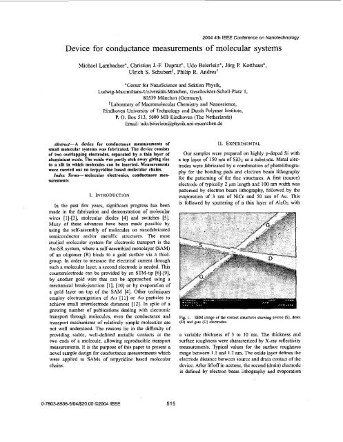
2004 4th IEEE Conference on Nanotechnology Device for conductance measurements of molecular systems Michael Lambacher*, Christian Dupraz*, Udo Beierlein*, Jorg P. Kotthaus*, Ulrich S. Schubertt, Philip R. Andrest *Center for NanoScience and Sektion Physik, Ludwig-Maximilians-Universitit-Miinchen, Geschwister-Scholl-Platz 1, 80539 Miinchen (Germany), t Laboratory of Macromolecular Chemistry and Nanoscience, Eindhoven University of Technology and Dutch Polymer Institute, P. 0. Box 513, 5600 MB Eindhoven (The Netherlands) Email: udo.heierlein@physik.uni-muenchen.de AbsfrabA device for conductance measurements of small molecular systems was fabricated. The device consists of two overlapping electrodes, separated by a thin layer of aluminium oxide. The oxide was partly etch away giving rise to a slit in which molecules can he inserted. Measurements were carried out on terpyridine based molecular chains. Index Term- molecular electronics, conductance measurements I. INTRODUCTION In the past few years, significant progress has been made in the fabrication and demonstration of molecular wires [I]-[3], molecular diodes [4] and switches [SI. Many of these advances have been made possible by using the self-assembly of molecules on nanofabricated semiconductor andlor metallic structures. The most studied molecular system for electronic transport is the Au-SR system, where a self-assembled monolayer (SAM) of an oligomer (R) binds to a gold surface via a thiolgroup. In order to measure the electrical current through such a molecular layer, a second electrode is needed. This counterelectrode can he provided by an STM-tip [6]-[9], by another gold wire that can be approached using a mechanical break-junction [l], [lo] or by evaporation of a gold layer on top of the SAM [4]. Other techniques employ electromigration of Au [l 11 or Au particles to achieve small interelectrode distances [12]. In spite of a growing number of publications dealing with electronic transport through molecules, even the conductance and transport mechanisms of relatively simple molecules are not well understood. The reasons lie in the difficulty of providing stable, well-defined metallic contacts at the two ends of a molecule, allowing reproducible transport measurements. It is the purpose of this paper to present a navel sample design for conductance measurements which were applied to SAMs of terpyridine based molecular chains. 11. EXPERIMENTAL Our samples were prepared on highly p-doped Si with a top layer of 150 nm of SiOz as a substrate. Metal electrodes were fabricated by a combination of photolithography for the bonding pads and electron beam lithography for the patterning of the fine structures. A fmt (source) electrode of typically 2 pm length and 100 nm width was panemed by electron beam lithography, followed by the evaporation of 3 nm of NiCr and 50 m of Au. This is followed by sputtering of a thin layer of A1203 with Fig. 1. SEM image of the contact shuchxcs showing Source (S), drain (D) and gate (F) electrodes. a variable thickness of 3 to 10 nm. The thickness and surface roughness were characterized by X-ray reflectivity measurements. Typical values for the surface roughness range between 1.1 and 1.2 nm. The oxide layer defines the electrode distance between source and drain contact of the device. After liftoff in acetone, the second (drain) electrode is defined by electron beam lithography and evaporation 0-7803-8536-5/04/$20.00 02004 IEEE 515
- Page 2 and 3: of 50 nm of gold such that it overl
2004 4th <strong>IEEE</strong> Conference on Nanotechnology<br />
<strong>Device</strong> <strong>for</strong> <strong>conductance</strong> <strong>measurements</strong> <strong>of</strong> <strong>molecular</strong> systems<br />
Michael Lambacher*, Christian Dupraz*, Udo Beierlein*, Jorg P. Kotthaus*,<br />
Ulrich S. Schubertt, Philip R. Andrest<br />
*Center <strong>for</strong> NanoScience and Sektion Physik,<br />
Ludwig-Maximilians-Universitit-Miinchen, Geschwister-Scholl-Platz 1,<br />
80539 Miinchen (Germany),<br />
t Laboratory <strong>of</strong> Macro<strong>molecular</strong> Chemistry and Nanoscience,<br />
Eindhoven University <strong>of</strong> Technology and Dutch Polymer Institute,<br />
P. 0. Box 513, 5600 MB Eindhoven (The Netherlands)<br />
Email: udo.heierlein@physik.uni-muenchen.de<br />
AbsfrabA device <strong>for</strong> <strong>conductance</strong> <strong>measurements</strong> <strong>of</strong><br />
small <strong>molecular</strong> systems was fabricated. The device consists<br />
<strong>of</strong> two overlapping electrodes, separated by a thin layer <strong>of</strong><br />
aluminium oxide. The oxide was partly etch away giving rise<br />
to a slit in which molecules can he inserted. Measurements<br />
were carried out on terpyridine based <strong>molecular</strong> chains.<br />
Index Term- <strong>molecular</strong> electronics, <strong>conductance</strong> <strong>measurements</strong><br />
I. INTRODUCTION<br />
In the past few years, significant progress has been<br />
made in the fabrication and demonstration <strong>of</strong> <strong>molecular</strong><br />
wires [I]-[3], <strong>molecular</strong> diodes [4] and switches [SI.<br />
Many <strong>of</strong> these advances have been made possible by<br />
using the self-assembly <strong>of</strong> molecules on nan<strong>of</strong>abricated<br />
semiconductor andlor metallic structures. The most<br />
studied <strong>molecular</strong> system <strong>for</strong> electronic transport is the<br />
Au-SR system, where a self-assembled monolayer (SAM)<br />
<strong>of</strong> an oligomer (R) binds to a gold surface via a thiolgroup.<br />
In order to measure the electrical current through<br />
such a <strong>molecular</strong> layer, a second electrode is needed. This<br />
counterelectrode can he provided by an STM-tip [6]-[9],<br />
by another gold wire that can be approached using a<br />
mechanical break-junction [l], [lo] or by evaporation <strong>of</strong><br />
a gold layer on top <strong>of</strong> the SAM [4]. Other techniques<br />
employ electromigration <strong>of</strong> Au [l 11 or Au particles to<br />
achieve small interelectrode distances [12]. In spite <strong>of</strong> a<br />
growing number <strong>of</strong> publications dealing with electronic<br />
transport through molecules, even the <strong>conductance</strong> and<br />
transport mechanisms <strong>of</strong> relatively simple molecules are<br />
not well understood. The reasons lie in the difficulty <strong>of</strong><br />
providing stable, well-defined metallic contacts at the<br />
two ends <strong>of</strong> a molecule, allowing reproducible transport<br />
<strong>measurements</strong>. It is the purpose <strong>of</strong> this paper to present a<br />
navel sample design <strong>for</strong> <strong>conductance</strong> <strong>measurements</strong> which<br />
were applied to SAMs <strong>of</strong> terpyridine based <strong>molecular</strong><br />
chains.<br />
11. EXPERIMENTAL<br />
Our samples were prepared on highly p-doped Si with<br />
a top layer <strong>of</strong> 150 nm <strong>of</strong> SiOz as a substrate. Metal electrodes<br />
were fabricated by a combination <strong>of</strong> photolithography<br />
<strong>for</strong> the bonding pads and electron beam lithography<br />
<strong>for</strong> the patterning <strong>of</strong> the fine structures. A fmt (source)<br />
electrode <strong>of</strong> typically 2 pm length and 100 nm width was<br />
panemed by electron beam lithography, followed by the<br />
evaporation <strong>of</strong> 3 nm <strong>of</strong> NiCr and 50 m <strong>of</strong> Au. This<br />
is followed by sputtering <strong>of</strong> a thin layer <strong>of</strong> A1203 with<br />
Fig. 1. SEM image <strong>of</strong> the contact shuchxcs showing Source (S), drain<br />
(D) and gate (F) electrodes.<br />
a variable thickness <strong>of</strong> 3 to 10 nm. The thickness and<br />
surface roughness were characterized by X-ray reflectivity<br />
<strong>measurements</strong>. Typical values <strong>for</strong> the surface roughness<br />
range between 1.1 and 1.2 nm. The oxide layer defines the<br />
electrode distance between source and drain contact <strong>of</strong> the<br />
device. After lift<strong>of</strong>f in acetone, the second (drain) electrode<br />
is defined by electron beam lithography and evaporation<br />
0-7803-8536-5/04/$20.00 02004 <strong>IEEE</strong> 515
<strong>of</strong> 50 nm <strong>of</strong> gold such that it overlaps the source electrode<br />
over an area <strong>of</strong> about 50 x 100 tun2. In the same step, gate<br />
electrodes can be patterned which approach the source and<br />
drain overlap area perpendicularly. The smallest distance<br />
<strong>of</strong> these gate electrodes to the source and drain electrodes<br />
is about 50 tun (Fig. I).<br />
Alternatively, similar overlapping electrode pairs with<br />
Alz03 oxide spacer can be defined only by optical lithography.<br />
In this case, the overlap area <strong>of</strong> source and drain<br />
electrodes is <strong>of</strong> the order <strong>of</strong> several pm2.<br />
In order to insert molecules between the source and the<br />
drain electrode, some nm <strong>of</strong> the A1203 layer is removed by<br />
wet etching in H3P04. Phosphoric acid selectively etches<br />
A1203 and leaves the underlying Si02 substrate intact. A<br />
cut through the device is shown schematically in Fig. 2 a).<br />
The molecules used in this study me depicted in Fig. 2<br />
applying a gate voltage.<br />
The preparation <strong>of</strong> <strong>molecular</strong> chains in our device was<br />
canied out in the following way: First, the samples were<br />
immersed into a 1 mM solution <strong>of</strong> molecule 1 in ethanol<br />
<strong>for</strong> a day or more in order to <strong>for</strong>m a self-assembled<br />
monolayer on the gold electrodes. Then, the samples were<br />
rinsed in pure ethanol. The sample was then transfered into<br />
a 1 mM solution <strong>of</strong> the linker-molecule 2 in chloro<strong>for</strong>m<br />
which was mixed with an equal amount <strong>of</strong> ethanol. A 1<br />
mM solution <strong>of</strong> CoClz in chloro<strong>for</strong>miethanol was added<br />
in order to initiate polymerization <strong>of</strong> the molecules. After<br />
several hours, the samples were removed from this solution<br />
and carefully rinsed in ethanol.<br />
Be<strong>for</strong>e insertion <strong>of</strong> the <strong>molecular</strong> chains, the samples were<br />
electrically tested. Only samples with low leakage currents<br />
<strong>of</strong> a few tens <strong>of</strong> pA at Vs,g = 1 V were used <strong>for</strong> the<br />
experiments. Typical breakthrough voltages <strong>of</strong> the oxide,<br />
e.g. <strong>for</strong> an oxide thickness <strong>of</strong> 10 nm, range between 1.8<br />
and 2.4 V.<br />
After build-up <strong>of</strong> the <strong>molecular</strong> chains, most samples show<br />
a significant increase <strong>of</strong> the source-drain current. Fig. 3<br />
shows an example <strong>of</strong> such a current measurement as a<br />
function <strong>of</strong> source-drain voltage at different temperatures.<br />
All curves, at T = 290, 77 and 4.2 K are almost linear,<br />
the current decreases as the temperature is lowered. Also<br />
shown is a curve be<strong>for</strong>e insertion <strong>of</strong> the molecules, with<br />
current values <strong>of</strong> 30 pA at VSD = 0.5 V. The inset in Fig.<br />
Fig. 2. a) Schematic viw <strong>of</strong> the device. The encircled area shows<br />
a molccular chain bctwccn source and drain clcctrodes. b) Molecules<br />
C19Hi9N3S~ and C~SHXNS used in this sbdy. Thc symbols conrspond<br />
10 tho drawing in a).<br />
h). Molecule 1 (C19H19N3S2, 4-(2,2’:6’,2”-terpyridin4’-<br />
ylsulfany1)-butane-I-thiol) consists <strong>of</strong> a terpyridine and a<br />
thiol endgroup, connected by a short alkyl chain. Linkermolecule<br />
2 (C36H24N6, 1,4-bis(terpyrid-4-yl)benzene) has<br />
terpyridine endgroups on both sides, with a phenylene<br />
ring in between. These molecules were chosen because<br />
<strong>of</strong> their ability to build stable coordination complexes in<br />
which a transition element atom, e.g. Cobalt, is bonded to<br />
two terpyridine groups. Using molecule 2, it is possible to<br />
create <strong>molecular</strong> chains which can bridge the gap between<br />
the source and drain electrode <strong>of</strong> our device. Park et al.<br />
[ll] have observed Coulomb blockade and the Kondo<br />
effect using similar molecules to molecule 1. These authors<br />
also showed that the charge state <strong>of</strong> CO atom in the<br />
coordination complex can be changed from 2+ to 3+ by<br />
1<br />
-0.6 -0.4 -0.2 0.0 0.2 0.4 0.6<br />
v, (v)<br />
Fig. 3. Current vcrsus sourcc-drain voltage <strong>of</strong> the dcvice with and<br />
without <strong>molecular</strong> chains at diffcrcnt tempcratwcs. Inset: Canductancc<br />
as B function <strong>of</strong> VSD at T = 4.2 K.<br />
3 depicts a <strong>conductance</strong> versus VsD curve at 4.2 K where<br />
peak structures are clearly seen. Note that other samples<br />
showed similar features, although the peak positions and<br />
the peak distances vary from sample to sample. Similar<br />
features were observed in other <strong>measurements</strong> using different<br />
molecules and different measurement techniques [13],<br />
-<br />
516
[14]. The molecules were removed afterwards by a piranha<br />
etch solution. In current <strong>measurements</strong> after removal <strong>of</strong><br />
the molecules currents <strong>of</strong> a few tens <strong>of</strong> pA where observed,<br />
similar to the <strong>measurements</strong> be<strong>for</strong>e insertion <strong>of</strong><br />
the molecules.<br />
The origin <strong>of</strong> the peaks is not very well understood.<br />
Coulomb blockade could cause such features if a conducting<br />
island is coupled by tunneling barriers to the source<br />
and drain contacts. Such islands could he created by the<br />
coordination complexes <strong>of</strong> the molecules, as proposed by<br />
Park et al. [I 11. But we could not observe any gate voltage<br />
dependence which could support this explanation. The<br />
observed <strong>conductance</strong> peaks could also be understood in<br />
terms <strong>of</strong> the vibrational modes <strong>of</strong> the molecule. Xbration<br />
<strong>of</strong> molecules would change the coupling between the orbitals<br />
<strong>of</strong> the molecules and the coupling <strong>of</strong> the molecules to<br />
the contacts. If the energy <strong>of</strong> the incident electron exceeds<br />
the vibrational energy, this could lead to variations in the<br />
current through the molecules due to energy transfer from<br />
the electrons to the molecule. Another explanation <strong>for</strong> the<br />
peaks is that these features may reflect coherent transport<br />
through the <strong>molecular</strong> orbitals. In this picture, the Fermi<br />
energy at zero bias would be located somewhere between<br />
the highest occupied <strong>molecular</strong> orbital (HOMO) and the<br />
lowest unoccupied <strong>molecular</strong> orbital (LUMO). As the<br />
source-drain voltage is increased, the current will increase<br />
due to resonant tunnelling when the potential <strong>of</strong> one <strong>of</strong><br />
the electrodes is equal to the nearest <strong>molecular</strong> level. By<br />
further increasing the potential difference between source<br />
and drain, more and more <strong>conductance</strong> channels will be<br />
opened giving rise to a <strong>conductance</strong> peak <strong>for</strong> every new<br />
<strong>molecular</strong> level.<br />
111. CONCLUSION<br />
We have developed a device <strong>for</strong> <strong>conductance</strong> <strong>measurements</strong><br />
<strong>of</strong> molecules which allows to reduce the electrode<br />
distance down to 3 nm. With this technique, it is possible<br />
to test the device be<strong>for</strong>e insertion and after removal <strong>of</strong><br />
the molecules giving more certainty that the obtained<br />
results really reflect the properties <strong>of</strong> the molecules. As<br />
an example, current and <strong>conductance</strong> <strong>measurements</strong> <strong>of</strong><br />
<strong>molecular</strong> chains bound to the electrodes by thiol groups<br />
were presented.<br />
[3] S.J. Tans, M.H. Devoret, H.J. Dai, A. Thess. R.E. Smallcy, L.J.<br />
Geerligs, C. Dekkcr, ”Individual single-wall carbon nanotubcs as<br />
quantum wircs”, Norure, vol. 386, pp. 474-477, ilpril 1997.<br />
[41 C. Zhou, M.R. Dcshpande, M.A. Reed, L. Jones, J.M.<br />
Tour:’Nanoscalc metal sclf-asscmbled monolayer metll<br />
heterostructurcs’’, Appl. Phys. Len., vol. 71, pp. 611-613, auyst<br />
1997.<br />
[5] J. Chen, M.A. Rccd, A.M. Rawlet& J.M. Tour, “Large on-<strong>of</strong>f ratios<br />
and negative differential resistance in a <strong>molecular</strong> electronic dcviec”,<br />
Science, vol. 286, pp. 1550-1552, november 1999. 1550.<br />
[61 L.A. Bu”, J.J. Arnold, M.T. Cygan, T.D. Dunbar, T.P. Bugin, L.<br />
Joncs 11, D.L. Allara, J.M. Tour, P.S. Wciss, ”Are single <strong>molecular</strong><br />
wires conducting?”, Science, vol. 271, pp. 1705-1707, mareh 1996.<br />
[7] R. P. Andrcs, T. Bein, M. Dorogi, S. Fag, J. I. Hcndcnon, C.P.<br />
Kubiak, W. Mahoncy, R.G. Osifchin, R. Reifcnberger, ””Coulomb<br />
staircase” at room temperature in a self-asscmbled malceular nanoitructure”,<br />
Science, vol. 272, pp. 1323-1325, may 1996.<br />
[81 X.D. Cui, A. Primak, X. Zaratc, J. Toomfohr, O.F. Sankey, A.L.<br />
Moore, T.A. Moore, D. Gust, G. Harris, S.M. Lindsay, ”Repmduciblc<br />
measouremcnt <strong>of</strong> single-molecule conductivily”, Science vol. 294, pp.<br />
571-574, October 2001.<br />
[9] S. Hang, R. Rcifenberger, W. Tian, S. Dam, J. Hcndcnon, C.P. Kubiak<br />
”Molccular Conductance spcctrooscopy <strong>of</strong> conjugated, phcnylbascd<br />
molecules on Au(l1 I): the effect <strong>of</strong> end groups on <strong>molecular</strong><br />
conduction”, Superlotiices Micmsmmci., vol. 28, 289-303, actobcr<br />
2000.<br />
[IO] J. Rcichert, R. Ochs, D. Bcckmam, H.B. Weber, M. Mayor, H.v.<br />
Lohncyscn, ”Driving current throuh single organic molecules”,<br />
Phys. Re. Len., vol. 88, pp. 176804, april 2002.<br />
[Ill J. Park, A.N. Pasupathy, J.I. Goldsmith, C: Chang, Y. Yaish, J.R.<br />
Pcna, M. Rinkoski, J.P. Sethna, H.D. Ab-a, P.L. McEucn, D.C.<br />
Ralph, ”Coulomb blockadc and the Kondo effect in singlc-atom<br />
transistors”, Nature. vol. 417, pp. 722-725, junc 2002.<br />
[I21 1. Amlani, A.M. Rawlett, L.A. Nagahara, R.K. Tsui, “An approach<br />
to transport <strong>measurements</strong> <strong>of</strong> Clcefronie molecules”, Appl. Phys.<br />
Len., vol. 80, pp. 2761-2763, april 1997.<br />
[I31 C. J.-F. Duprar, U. Bcicrlcin, J.P. Konhaus, ”Low tempcraturc<br />
conductancc mcasurementS <strong>of</strong> self-asscmblcd monolayers <strong>of</strong> 1.4-<br />
phcoylcnc diisocyanidc”, ChemPhySChem, vol. 4, pp. 1247.1252,<br />
novcmbcr 2003.<br />
[I41 J:O. Lee, G. Lientschnig, F. Wiertz, M. Struijk, R.A.J. Janscn,<br />
R. Egbcrink, D.N. Reinhoudt, P. Hadley, C. Dckker, ”Absence <strong>of</strong><br />
strong gate cffcce in electrical mcasurcments on phenylene-bascd<br />
conjugatcd molccules”, Nano Len., vol. 3, pp. 113.1 17, fcbruary<br />
2003.<br />
ACKNOWLEDGMENT<br />
We would like to thank G. Abstreiter and M. Tomow<br />
<strong>for</strong> stimulating discussions. Financial support by the Sonder<strong>for</strong>scbungsbereicb<br />
486 is gratefully acknowledged.<br />
REFERENCES<br />
[I1 M.A. Reed, C. Zhau, C.J. Muller, T.P. Burgin, J.M. Toour, ”Conductance<br />
<strong>of</strong> a <strong>molecular</strong> junction”, Sciencc, vol. 278. pp. 252-254,<br />
octobcr 1997.<br />
121 M.A. Reed, ”Molecular-scale electronics”, Pmc <strong>IEEE</strong>, vol. 87, pp.<br />
652-658, apd 1999.<br />
517


