Transistor Common Base Configuration Common Emitter ...
Transistor Common Base Configuration Common Emitter ...
Transistor Common Base Configuration Common Emitter ...

You also want an ePaper? Increase the reach of your titles
YUMPU automatically turns print PDFs into web optimized ePapers that Google loves.
5/1/2011<br />
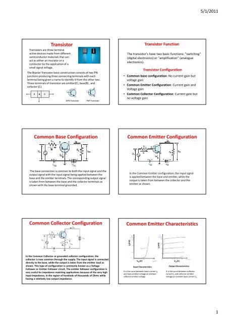
<strong>Transistor</strong><br />
<strong>Transistor</strong>s are three terminal<br />
active devices made from different<br />
semiconductor materials that can<br />
act as either an insulator or a<br />
conductor by the application of a<br />
small signal voltage.<br />
The Bipolar <strong>Transistor</strong> basic construction consists of two PNjunctions<br />
producing three connecting terminals with each<br />
terminal being given a name to identify it from the other two.<br />
Three terminals of transistor are emitter(E), base(B) , and<br />
collector (C).<br />
E B C<br />
NPN <strong>Transistor</strong><br />
PNP <strong>Transistor</strong><br />
<strong>Transistor</strong> Function<br />
The transistor's have two basic functions: "switching"<br />
(digital electronics) or "amplification" (analogue<br />
electronics).<br />
<strong>Transistor</strong> <strong>Configuration</strong><br />
• <strong>Common</strong> base configuration: No current gain but<br />
voltage gain<br />
• <strong>Common</strong> <strong>Emitter</strong> <strong>Configuration</strong>: Current gain and<br />
Voltage gain<br />
• <strong>Common</strong> Collector <strong>Configuration</strong>: Current gain but<br />
no voltage gain<br />
<strong>Common</strong> <strong>Base</strong> <strong>Configuration</strong><br />
<strong>Common</strong> <strong>Emitter</strong> <strong>Configuration</strong><br />
The base connection is common to both the input signal and the<br />
output signal with the input signal being applied between the<br />
base and the emitter terminals. The corresponding output signal<br />
is taken from between the base and the collector terminals as<br />
shown with the base terminal grounded.<br />
In the <strong>Common</strong> <strong>Emitter</strong> configuration, the input signal<br />
is applied between the base and emitter, while the<br />
output is taken from between the collector and the<br />
emitter as shown.<br />
<strong>Common</strong> Collector <strong>Configuration</strong><br />
<strong>Common</strong> <strong>Emitter</strong> Characteristics<br />
I B (mA)<br />
I C (mA)<br />
In the <strong>Common</strong> Collector or grounded collector configuration, the<br />
collector is now common through the supply. The input signal is connected<br />
directly to the base, while the output is taken from the emitter load as<br />
shown. This type of configuration is commonly known as a Voltage<br />
Follower or <strong>Emitter</strong> Follower circuit. The emitter follower configuration is<br />
very useful for impedance matching applications because of the very high<br />
input impedance, in the region of hundreds of thousands of Ohms while<br />
having a relatively low output impedance.<br />
V BE (V)<br />
Input Characteristics<br />
It is the curve between base current I B<br />
and base-emitter voltage at constant<br />
collector emitter voltage<br />
V CE (V)<br />
Output Characteristics<br />
It is the curve between collector<br />
current I C and collector-emitter<br />
voltage at constant base current I B .<br />
1
5/1/2011<br />
<strong>Transistor</strong> Characteristics Regions<br />
Bipolar <strong>Transistor</strong> has<br />
mainly three reasons.<br />
1. Active Region - the<br />
transistor operates as<br />
an amplifier.<br />
2. Saturation - the<br />
transistor is "fully-ON"<br />
operating as a switch.<br />
3. Cut-off - the transistor<br />
is "fully-OFF" operating as<br />
a switch.<br />
Relations of Current amplification<br />
factor<br />
The ratio of change in collector current<br />
to the change in emitter current at<br />
constant collector-base voltage is<br />
known as current amplification factor.<br />
The ratio of change in collector current<br />
to the change in base current is known<br />
as base current amplification factor.<br />
I<br />
C<br />
= α I<br />
E<br />
= β I<br />
β<br />
α =<br />
β + 1<br />
B<br />
I = I + I<br />
E<br />
β =<br />
C<br />
α<br />
α −1<br />
I<br />
α =<br />
I<br />
I<br />
β =<br />
I<br />
B<br />
C<br />
E<br />
C<br />
B<br />
How <strong>Transistor</strong> acts as an Amplifier?<br />
Field Effect <strong>Transistor</strong><br />
A transistor BE junction has a low<br />
resistance due to forward bias and the<br />
BC junction has a high resistance due to<br />
reverse bias. A transistor amplifies<br />
current because the collector current is<br />
equal to the base current multiplied by<br />
the current gain.<br />
Let us consider the following circuit<br />
An ac voltage, V in , is superimposed on<br />
the dc bias voltage V BB . DC bias voltage<br />
V CC is connected to the collector<br />
through the collector resistance, R C .<br />
The ac input voltage produces an ac base current, which<br />
results in a much larger ac collector current. The ac<br />
collector current produces an ac voltage across R C , thus<br />
producing an amplified, but inverted, reproduction of the<br />
ac input voltage in the active region.<br />
Input<br />
Output<br />
JFET Operation<br />
With no external Gate voltage ( VG = 0 ), and a small<br />
voltage ( VDS ) applied between the Drain and the<br />
Source, maximum saturation current ( IDSS ) will<br />
flow through the channel from the Drain to the<br />
Source restricted only by the small depletion region<br />
around the junctions.<br />
If a small negative voltage ( -VGS ) is now applied to the Gate the size of the depletion<br />
region begins to increase reducing the overall effective area of the channel and thus<br />
reducing the current flowing through it, a sort of "squeezing" effect takes place. So by<br />
applying a reverse bias voltage increases the width of the depletion region which in turn<br />
reduces the conduction of the channel..<br />
Since the PN-junction is reverse biased, little current will flow into the gate connection.<br />
As the Gate voltage ( -VGS ) is made more negative, the width of the channel decreases<br />
until no more current flows between the Drain and the Source and the FET is said to be<br />
"pinched-off" (similar to the cut-off region for a BJT)<br />
JFET Characteristics<br />
Ohmic Region - When VGS = 0 the depletion<br />
layer of the channel is very small and the JFET<br />
acts like a voltage controlled resistor.<br />
Cut-off Region - This is also known as the<br />
pinch-off region were the Gate voltage, VGS is<br />
sufficient to cause the JFET to act as an open<br />
circuit as the channel resistance is at<br />
maximum.<br />
Saturation or Active Region - The JFET<br />
becomes a good conductor and is controlled<br />
by the Gate-Source voltage, ( VGS ) while the<br />
Drain-Source voltage, ( VDS ) has little or no<br />
effect.<br />
Breakdown Region - The voltage between the Drain and the Source, ( VDS ) is high<br />
enough to causes the JFET's resistive channel to break down and pass uncontrolled<br />
maximum current.<br />
2
5/1/2011<br />
FET Parameters<br />
DC Drain Resistance is the static or ohmic resistance of the channel<br />
and is given by R DS = V DS /I D .<br />
AC Drain Resistance is the ratio of change in drain source voltage<br />
(ΔV DS ) and change in drain current (ΔI D ) at constant gate-source<br />
voltage V GS . It is also called the dynamic resistance and denoted as<br />
rd.<br />
Transconductance g m is the ratio of change in drain current (ΔI D ) to the<br />
change in gate-source voltage (ΔV GS ) at constant V DS .<br />
Amplification Factor is defined as the ratio of change in V DS to the<br />
change in V GS at constant drain current and is denoted by µ<br />
Comparison between BJT and FET<br />
Field Effect <strong>Transistor</strong> (FET) Bipolar Junction <strong>Transistor</strong> (BJT)<br />
1 Low voltage gain High voltage gain<br />
2 High current gain Low current gain<br />
3 Very input impedance Low input impedance<br />
4 High output impedance Low output impedance<br />
5 Low noise generation Medium noise generation<br />
6 Fast switching time Medium switching time<br />
7 Easily damaged by static Robust<br />
8 Some require an input to Requires zero input to turn it "OFF"<br />
turn it "OFF"<br />
9 Voltage controlled device Current controlled device<br />
10 Exhibits the properties of a Resistor<br />
11 More expensive than bipolar Cheap<br />
12 Difficult to bias Easy to bias<br />
Classification of FET<br />
3