Gas transport controlled synthesis of graphene by employing a ...
Gas transport controlled synthesis of graphene by employing a ...
Gas transport controlled synthesis of graphene by employing a ...

You also want an ePaper? Increase the reach of your titles
YUMPU automatically turns print PDFs into web optimized ePapers that Google loves.
Electronic Supplementary Material (ESI) for RSC Advances<br />
This journal is © The Royal Society <strong>of</strong> Chemistry 2013<br />
Electronic Supplementary Information<br />
<strong>Gas</strong> <strong>transport</strong> <strong>controlled</strong> <strong>synthesis</strong> <strong>of</strong> <strong>graphene</strong> <strong>by</strong> <strong>employing</strong> a<br />
micro-meter scale gap jig<br />
Seong-Yong Cho, a Ki-Ju Kim, a Hyun-Mi Kim, a Do-Joong Lee, a Min-Hyun Lee a and Ki-Bum Kim* a b<br />
a Department <strong>of</strong> Materials Science and Engineering, Seoul National University, Seoul 151-742, Korea<br />
b WCU Hybrid Materials Program, Department <strong>of</strong> Materials Science and Engineering, Seoul National<br />
University, Seoul 151-742, Korea<br />
Raman spectra were recorded for the <strong>graphene</strong> sample after the transfer. Using extended growth times,<br />
such as 30 min, continuous <strong>graphene</strong> films were successfully grown on the entire copper foil. The full<br />
width at half maximum <strong>of</strong> the 2D peak was 37 cm -1 , indicating a high-quality single layer <strong>of</strong> <strong>graphene</strong><br />
(Fig. S1 (a)). For the case <strong>of</strong> partially grown <strong>graphene</strong> islands, the optical microscopy images were<br />
almost the same as the SEM images before the transfer (Fig. S1 (b) and (c)).<br />
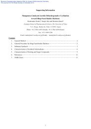
Fig. S1 - (a) Typical Raman spectrum <strong>of</strong> <strong>graphene</strong> fully grown on Cu foil after the transfer to a SiO 2<br />
(285 nm)/Si substrate when the jig is applied after an extended growth time <strong>of</strong> 30 min. (b) Optical<br />
microscope image <strong>of</strong> <strong>graphene</strong> islands after transfer. (c) G-band micro-Raman mapping analysis over<br />
a 50 × 50 µm area with a step size <strong>of</strong> 1 µm for the area depicted in (b). A 532-nm DSSP laser and<br />
X100 objective lens were used.
Electronic Supplementary Material (ESI) for RSC Advances<br />
This journal is © The Royal Society <strong>of</strong> Chemistry 2013<br />
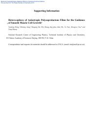
Fig. S2 - SEM images <strong>of</strong> <strong>graphene</strong> grown on Cu foil when a micrometer-gap jig is applied for gas<br />
<strong>transport</strong> control. SEM images <strong>of</strong> (a) the fully grown <strong>graphene</strong> film on the jig exterior, (b) 5 mm from<br />
the jig entrance, (c) 10 mm from the jig entrance, (d) 15 mm from the jig entrance, and (e) 20 mm<br />
from the jig entrance. CH 4 and H 2 flux: 2 sccm and 6 sccm, respectively. Scale bar indicates 50 µm.