A 24 Gb/s Software Programmable Analog Multi-Tone - Research ...
A 24 Gb/s Software Programmable Analog Multi-Tone - Research ...
A 24 Gb/s Software Programmable Analog Multi-Tone - Research ...

You also want an ePaper? Increase the reach of your titles
YUMPU automatically turns print PDFs into web optimized ePapers that Google loves.
AMIRKHANY et al.: A <strong>24</strong> GB/S SOFTWARE PROGRAMMABLE ANALOG MULTI-TONE TRANSMITTER 1003<br />
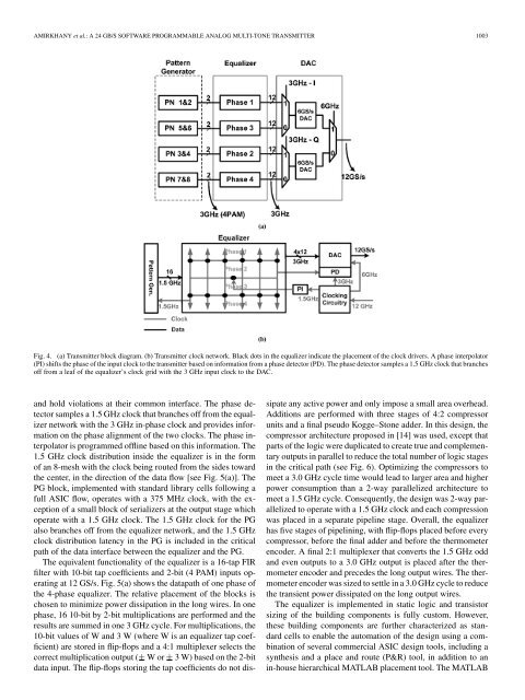
Fig. 4. (a) Transmitter block diagram. (b) Transmitter clock network. Black dots in the equalizer indicate the placement of the clock drivers. A phase interpolator<br />
(PI) shifts the phase of the input clock to the transmitter based on information from a phase detector (PD). The phase detector samples a 1.5 GHz clock that branches<br />
off from a leaf of the equalizer’s clock grid with the 3 GHz input clock to the DAC.<br />
and hold violations at their common interface. The phase detector<br />
samples a 1.5 GHz clock that branches off from the equalizer<br />
network with the 3 GHz in-phase clock and provides information<br />
on the phase alignment of the two clocks. The phase interpolator<br />
is programmed offline based on this information. The<br />
1.5 GHz clock distribution inside the equalizer is in the form<br />
of an 8-mesh with the clock being routed from the sides toward<br />
the center, in the direction of the data flow [see Fig. 5(a)]. The<br />
PG block, implemented with standard library cells following a<br />
full ASIC flow, operates with a 375 MHz clock, with the exception<br />
of a small block of serializers at the output stage which<br />
operate with a 1.5 GHz clock. The 1.5 GHz clock for the PG<br />
also branches off from the equalizer network, and the 1.5 GHz<br />
clock distribution latency in the PG is included in the critical<br />
path of the data interface between the equalizer and the PG.<br />
The equivalent functionality of the equalizer is a 16-tap FIR<br />
filter with 10-bit tap coefficients and 2-bit (4 PAM) inputs operating<br />
at 12 GS/s. Fig. 5(a) shows the datapath of one phase of<br />
the 4-phase equalizer. The relative placement of the blocks is<br />
chosen to minimize power dissipation in the long wires. In one<br />
phase, 16 10-bit by 2-bit multiplications are performed and the<br />
results are summed in one 3 GHz cycle. For multiplications, the<br />
10-bit values of W and 3 W (where W is an equalizer tap coefficient)<br />
are stored in flip-flops and a 4:1 multiplexer selects the<br />
correct multiplication output ( Wor 3 W) based on the 2-bit<br />
data input. The flip-flops storing the tap coefficients do not dissipate<br />
any active power and only impose a small area overhead.<br />
Additions are performed with three stages of 4:2 compressor<br />
units and a final pseudo Kogge–Stone adder. In this design, the<br />
compressor architecture proposed in [14] was used, except that<br />
parts of the logic were duplicated to create true and complementary<br />
outputs in parallel to reduce the total number of logic stages<br />
in the critical path (see Fig. 6). Optimizing the compressors to<br />
meet a 3.0 GHz cycle time would lead to larger area and higher<br />
power consumption than a 2-way parallelized architecture to<br />
meet a 1.5 GHz cycle. Consequently, the design was 2-way parallelized<br />
to operate with a 1.5 GHz clock and each compression<br />
was placed in a separate pipeline stage. Overall, the equalizer<br />
has five stages of pipelining, with flip-flops placed before every<br />
compressor, before the final adder and before the thermometer<br />
encoder. A final 2:1 multiplexer that converts the 1.5 GHz odd<br />
and even outputs to a 3.0 GHz output is placed after the thermometer<br />
encoder and precedes the long output wires. The thermometer<br />
encoder was sized to settle in a 3.0 GHz cycle to reduce<br />
the transient power dissipated on the long output wires.<br />
The equalizer is implemented in static logic and transistor<br />
sizing of the building components is fully custom. However,<br />
these building components are further characterized as standard<br />
cells to enable the automation of the design using a combination<br />
of several commercial ASIC design tools, including a<br />
synthesis and a place and route (P&R) tool, in addition to an<br />
in-house hierarchical MATLAB placement tool. The MATLAB