Selection Guide 2013 - Ricoh
Selection Guide 2013 - Ricoh
Selection Guide 2013 - Ricoh

You also want an ePaper? Increase the reach of your titles
YUMPU automatically turns print PDFs into web optimized ePapers that Google loves.
Power Management ICs (Voltage Regulator)<br />
New : Under Development :<br />
Lineup in order of Input Voltage (Max.) and Output Current<br />
Major products are classified by function. This chart does not include all products.<br />
Input Voltage (Max.) up to 6.5V<br />
Input<br />
Output Current<br />
Type<br />
Voltage ~ 150mA<br />
~ 300mA<br />
(Max.)<br />
~ 200mA<br />
Single Dual Single Dual<br />
~ 400mA ~ 500mA ~ 800mA ~ 1A ~ 1.5A ~ 2A ~ 3A<br />
5.25V RP112x RP102x RP150K RP111x<br />
High-performance Type<br />
6.0V<br />
R1172x<br />
R1173x<br />
6.5V RP130x<br />
3.6V<br />
RP106x<br />
RP116Z<br />
RP109x RP152x RP100x RP101x RP154x RP105x RP115L<br />
5.25V<br />
RP115x *1 RP108J<br />
Standard Type<br />
RP153L<br />
RP114x<br />
6.0V R1170x R1171S R1171J<br />
6.5V<br />
RP131x<br />
RP132x<br />
Low Supply Current Type<br />
5.25V RP110x<br />
6.0V R1180x<br />
5.25V RP202x<br />
Automatic mode shift type<br />
6.0V R5326K<br />
ECO<br />
Manual/Automatic mode shift type 5.25V RP201x<br />
Functions<br />
Seamless type<br />
R1116x<br />
6.0V<br />
Manual mode shift type R1163x R5328K R1160N<br />
RP200x<br />
*1) RP115L (DFN1216-8) has an LCON pin to switch between 500mA and 1A output current.<br />
Input Voltage (Max.) from 8.0V to 36.0V<br />
Input<br />
Output Current<br />
Type<br />
Voltage<br />
(Max.)<br />
~ 150mA ~ 300mA ~ 500mA ~ 1A<br />
8V<br />
R1111N<br />
R1130H<br />
R1121N<br />
Standard Type<br />
10V RP171x RP170x<br />
16V<br />
R1190x<br />
24V R1500H R1501x<br />
36V R1516x R1511x<br />
8V<br />
Rx5RW (~80mA)<br />
Rx5RZ (~100mA)<br />
10V Rx5RL (~80mA)<br />
11V RP173x<br />
Low Supply Current Type<br />
R1150H +VD<br />
24V<br />
R1154x<br />
36V<br />
R1515x (50mA)<br />
R1517x R1518x<br />
R1514x<br />
Manual mode shift type 16V R1191x<br />
ECO<br />
24V<br />
R1155x<br />
Functions Automatic mode shift type<br />
36V<br />
R1510S +VD<br />
Ext. PNP Tr. type 10V RN5RF<br />
*1) RP173x : VSET+6.5V ≤ 11.0V<br />
Lineup in order of Specification (Output Current 25mA to 120mA)<br />
ECO Function Seamless : Seamless type Manual : Manual mode shift type Automatic : Automatic mode shift type Manual / Automatic : Manual / Automatic mode shift type<br />
<br />
Thermal : Thermal Shutdown Circuit Slope : Constant Slope Circuit Reverse : Reverse Current Protection Circuit Inrush : Inrush Current Limit Circuit<br />
Succeeding products are available for products highlighted in grey rows. We recommend the products shown in "Other functions".<br />
Rxxxx<br />
• Products partially available for automotive applications. Products for automotive applications may not provide all specifications of products for consumer applications.<br />
Please refer to the "CAR ELECTRONICS PRODUCTS Catalog" for additional details.<br />
Supply<br />
Product Output Input Voltage Output Voltage Voltage Dropout Voltage *A<br />
Current RR@1kHz Capacitance of output<br />
ceramic capacitor<br />
Name Current Range Range Accuracy<br />
Typ. Max. Condition Typ. Typ. /Other functions<br />
Package<br />
Rx5RL 25 to 55mA Max. 10.0V 2.0V to 6.0V ±2.5% 0.04V 0.06V IOUT=1mA 1μA — 0.1μF to 2.2μF<br />
SOT-23-5,<br />
SOT-89<br />
Rx5RW 35 to 80mA Max. 8.0V 1.5V to 6.0V ±2% 0.04V 0.06V IOUT=1mA 1.5μA — 0.1μF to 2μF<br />
SON1612-6,<br />
SC-82AB<br />
R1100D 35 to 100mA Max. 6.0V 0.9V to 4.0V ±2% 0.025V 0.05V IOUT=1mA 1.5μA — 0.1μF or more SON1408-3<br />
RN5RT 40 to 100mA Max. 8.0V 2.0V to 6.0V ±2% 0.3V 0.5V IOUT=40mA 4μA — 0.1μF to 2.2μF SOT-23-5<br />
R1515x • 50mA 4.0V to 36.0V 2.0V to 12.0V ±2% 0.20V 0.35V<br />
0.1μF to 10μF<br />
IOUT=20mA<br />
9μA — Operating Temp.: -40 to 105°C<br />
SOT-89-5,<br />
VSET=5.0V<br />
HSOP-6J<br />
Thermal<br />
RH5RE 60 to 120mA Max. 10.0V 2.0V to 6.0V ±2.5% 0.5V 0.7V IOUT=30mA 1.1μA — 0.1μF to 2.2μF SOT-89<br />
Rx5RZ 100mA Max. 8.0V 2.0V to 6.0V ±2% 0.2V 0.3V IOUT=60mA 20μA 55dB Tantalum 10μF or more<br />
R1141Q 120mA 2.2V to 6.0V 1.5V to 4.0V ±1.5% 0.18V 0.28V IOUT=120mA 90μA 70dB<br />
1μF to 2.2μF or more<br />
RP109x<br />
SOT-23-5,<br />
SOT-89<br />
SC-82AB
2 0 1 3<br />
New :<br />
Lineup in order of Specification (Output Current 150mA)<br />
ECO Function Seamless : Seamless type Manual : Manual mode shift type Automatic : Automatic mode shift type Manual / Automatic : Manual / Automatic mode shift type<br />
Thermal : Thermal Shutdown Circuit Slope : Constant Slope Circuit Reverse : Reverse Current Protection Circuit Inrush : Inrush Current Limit Circuit<br />
Succeeding products are available for products highlighted in grey rows. We recommend the products shown in "Other functions".<br />
Rxxxx<br />
• Products partially available for automotive applications. Products for automotive applications may not provide all specifications of products for consumer applications.<br />
Please refer to the "CAR ELECTRONICS PRODUCTS Catalog" for additional details.<br />
Product<br />
Name<br />
Output<br />
Current<br />
Input Voltage<br />
Range<br />
RP103x 150mA 1.7V to 5.25V 1.2V to 3.3V ±1% 0.21V 0.27V IOUT=150mA 36μA 75dB<br />
RP104x 150mA 1.7V to 5.25V 1.2V to 3.3V ±0.8% 0.24V 0.32V IOUT=150mA 1μA —<br />
RP109x 150mA 1.4V to 5.25V 0.8V to 3.6V ±1% 0.25V 0.35V IOUT=150mA 50μA 75dB<br />
RP110x 150mA 1.4V to 5.25V 0.8V to 3.6V ±1% 0.28V 0.40V IOUT=150mA 1μA —<br />
RP112x 150mA 2.0V to 5.25V 1.2V to 4.8V ±1% 0.20V 0.28V IOUT=150mA 75μA<br />
RP130x • 150mA 1.7V to 6.5V 1.2V to 5.3V ±1% 0.32V 0.51V IOUT=150mA 38μA 80dB<br />
RP171x • 150mA 2.6V to 10.0V 1.2V to 6.0V ±1% 0.40V 0.56V IOUT=150mA 23μA 70dB<br />
RP173x 150mA 2.5V to 11.0V *3 1.2V to 5.5V ±1% 0.90V 1.47V IOUT=150mA 2μA —<br />
RP201x 150mA 1.4V to 5.25V 0.8V to 4.0V ±1% *1 0.12V *1 0.18V *1 IOUT=150mA<br />
55μA *1<br />
(1.5μA)<br />
R1111N 150mA 2.0V to 8.0V 1.5V to 5.0V ±2% 0.2V 0.3V IOUT=100mA 35μA 70dB<br />
R1114x • 150mA 2.0V to 6.0V 1.5V to 4.0V ±2% 0.22V 0.35V IOUT=150mA 75μA 70dB<br />
0.47μF or more<br />
DFN(PLP)1010-4,<br />
Temp. Coeff.:Typ.±30ppm/°C SC-82AB,<br />
RP109x<br />
SOT-23-5<br />
0.1μF or more<br />
Temp. Coeff.:Typ.±40ppm/°C<br />
RP110x<br />
0.1μF or more<br />
Load regulation:Typ. 5mV<br />
Temp. Coeff.:Typ.±30ppm/°C<br />
0.1μF or more<br />
Slope<br />
1μF or more<br />
80dB,<br />
Output noise:10μVrms<br />
65dB *2<br />
Temp. Coeff.:Typ.±30ppm/°C<br />
70dB *1<br />
0.47μF or more<br />
Temp. Coeff.:Typ.±20ppm/°C<br />
1μF or more<br />
Thermal Slope<br />
0.1μF or more<br />
Reverse<br />
1μF or more<br />
Manual / Automatic<br />
DFN(PLP)1010-4,<br />
SOT-23-5<br />
DFN(PLP)0808-4,<br />
DFN1010-4,<br />
SC-88A,<br />
SOT-23-5<br />
DFN(PLP)0808-4,<br />
DFN1010-4,<br />
SC-88A,<br />
SOT-23-5<br />
DFN(PLP)1010-4,<br />
SC-88A,<br />
SOT-23-5<br />
DFN(PLP)1010-4,<br />
SC-82AB,<br />
SOT-23-5<br />
SC-88A,<br />
SOT-23-5<br />
DFN(PLP)1010-4,<br />
SC-88A,<br />
SOT-23-5<br />
WLCSP-4-P5,<br />
DFN(PLP)1212-6<br />
Tantalum 10μF or more<br />
Replaceable with LP2980/2985 SOT-23-5<br />
0.47μF to 1μF or more<br />
RP109x, RP130x<br />
R1116x 150mA 1.8V to 6.0V 1.5V to 4.0V ±1.5% 0.29V 0.46V IOUT=150mA 10μA 70dB 1μF or more Seamless<br />
R1118K 150mA 1.4V to 6.0V 0.8V to 4.2V ±1% 0.27V *1 0.37V *1 IOUT=150mA<br />
50μA *1<br />
(5.5μA)<br />
R1121N 150mA 2.0V to 8.0V 1.5V to 5.0V ±2% 0.2V 0.3V IOUT=100mA 35μA 70dB<br />
R1122N 150mA 2.0V to 6.0V 1.5V to 5.0V ±2% 0.19V 0.26V IOUT=100mA 100μA 80dB<br />
SON1612-6,<br />
SC-82AB,<br />
SOT-23-5<br />
SON1612-6,<br />
SOT-23-5<br />
*1 1μF or more Automatic<br />
70dB DFN(PLP)1612-4B<br />
RP201x, RP202x<br />
Tantalum 1μF or more<br />
Replaceable with TK111/112/113 SOT-23-5<br />
2.2μF to 4.7μF or more<br />
Replaceable with TK111/112/113 SOT-23-5<br />
RP112x, RP130x<br />
R1150H +VD • 150mA Max. 24.0V 2.1V to 14.0V ±2% 0.3V 0.4V IOUT=20mA 7μA — 0.1μF or more Thermal SOT-89-5<br />
R1154x 150mA Max. 24.0V<br />
R1155x 150mA 3.5V to 24.0V<br />
Output Voltage<br />
Range<br />
2.5V to 12.0V ±2%<br />
Ext. adjustable<br />
±50mV<br />
2.5V to 12.0V ±2%<br />
Ext. adjustable<br />
Voltage<br />
Accuracy<br />
±50mV<br />
0.2V 0.4V IOUT=20mA 5μA —<br />
1.0V 1.7V IOUT=150mA<br />
VSET=5.0V<br />
R1163x • 150mA 2.0V to 6.0V 1.5V to 5.0V ±1.5% *1 0.25V *1 0.35V *1 IOUT=150mA<br />
65μA *1<br />
(7.5μA)<br />
70μA *1<br />
(6μA)<br />
60dB *1<br />
0.1μF to 2.2μF<br />
Operating Temp.: -40 to 105°C<br />
Thermal<br />
4.7μF or more<br />
Operating Temp.: -40 to 105°C<br />
Thermal Reverse<br />
Automatic<br />
0.47μF or more<br />
*1<br />
70dB<br />
Reverse Manual<br />
R1180x • 150mA 1.7V to 6.0V 1.2V to 3.6V ±2% 0.25V 0.40V IOUT=150mA 1μA — 0.1μF or more<br />
R1183Z 150mA 1.7V to 6.0V 1.2V to 3.6V ±1.2% 0.25V 0.40V IOUT=150mA 1μA —<br />
R1514x • 150mA 4.0V to 36.0V 2.0V to 12.0V ±2% 0.20V 0.35V<br />
R1516x • 150mA 4.0V to 36.0V 1.8V to 6.2V ±1% — 0.60V<br />
IOUT=20mA<br />
VSET=5.0V<br />
IOUT=20mA<br />
VSET=5.0V<br />
9μA —<br />
29μA —<br />
*A) This value varies depending on the set output voltage, VSET=2.8V or close to 2.8V. (If described, value at the set output voltage.)<br />
*1) in Fast Mode, ( ) in Low Power Mode *2) RR@f=100kHz *3) VSET+6.5V ≤ 11.0V<br />
Dropout Voltage *A<br />
Supply<br />
Current RR@1kHz<br />
Typ. Max. Condition Typ. Typ.<br />
Capacitance of output<br />
ceramic capacitor<br />
/Other functions<br />
DFN1616-6,<br />
SOT-23-5,<br />
SOT-89-5<br />
SOT-23-5,<br />
SOT-89-5<br />
DFN(PLP)1616-6,<br />
SON-6,<br />
SOT-23-5<br />
SON1612-6,<br />
SC-82AB,<br />
SOT-23-5<br />
0.1μF or more<br />
WLCSP-4-P2<br />
RP110K<br />
0.1μF to 10μF<br />
Operating Temp.: -40 to 105°C<br />
SOT-89-5,<br />
HSOP-6J<br />
Thermal<br />
0.1μF to 20μF<br />
Operating Temp.: -40 to 105°C<br />
Thermal<br />
Package<br />
SOT-89-5,<br />
HSOP-6J
Power Management ICs (Voltage Regulator)<br />
New : Under Development :<br />
Lineup in order of Specification (Output Current 200mA to 800mA)<br />
ECO Function Seamless : Seamless type Manual : Manual mode shift type Automatic : Automatic mode shift type Manual / Automatic : Manual / Automatic mode shift type<br />
<br />
Thermal : Thermal Shutdown Circuit Slope : Constant Slope Circuit Reverse : Reverse Current Protection Circuit Inrush : Inrush Current Limit Circuit<br />
Succeeding products are available for products highlighted in grey rows. We recommend the products shown in "Other functions".<br />
Rxxxx<br />
• Products partially available for automotive applications. Products available for automotive applications only. Products for automotive applications may not provide<br />
all specifications of products for consumer applications. Please refer to the "CAR ELECTRONICS PRODUCTS Catalog" for additional details.<br />
Product<br />
Name<br />
Output<br />
Current<br />
Input Voltage<br />
Range<br />
Output Voltage<br />
Range<br />
Voltage<br />
Accuracy<br />
Dropout Voltage *A<br />
Supply<br />
Current<br />
RR@1kHz<br />
Typ. Max. Condition Typ. Typ.<br />
RP100x 200mA 1.7V to 5.25V 1.2V to 3.3V ±0.6% 0.13V 0.23V IOUT=150mA 18μA 75dB<br />
RP107x 200mA 1.4V to 5.25V 1.0V to 4.2V ±1% 0.27V 0.36V IOUT=200mA 9.5μA 60dB<br />
RP202x 200mA 1.4V to 5.25V 0.8V to 4.0V ±1% *1 0.20V *1 0.29V *1 IOUT=200mA<br />
R1160N 200mA 1.4V to 6.0V 0.8V to 3.3V ±2% *1 0.14V *1 0.2V *1<br />
(0.25V)<br />
IOUT=200mA<br />
50μA *1<br />
(2.5μA)<br />
40μA *1<br />
(4.5μA)<br />
70dB *1<br />
70dB *1<br />
RP101x 300mA 1.7V to 5.25V 1.2V to 3.3V ±0.6% 0.13V 0.23V IOUT=150mA 18μA 75dB<br />
RP102x 300mA 1.7V to 5.25V 1.2V to 3.3V ±0.8% 0.12V 0.19V IOUT=300mA 50μA 80dB<br />
Capacitance of output<br />
ceramic capacitor<br />
/Other functions<br />
Package<br />
1μF or more<br />
DFN(PLP)1612-4,<br />
Temp. Coeff.:Typ.±30ppm/°C SOT-23-5<br />
Output Capacitor-less WLCSP-4-P5,<br />
(CIN=0.1μF or more) DFN(PLP)1212-6,<br />
Slope<br />
SC-88A, SOT-23-5<br />
0.47μF or more<br />
Automatic Slope<br />
Tantalum 2.2μF or more<br />
Manual<br />
1μF or more<br />
Temp. Coeff.:Typ.±30ppm/°C<br />
1μF or more<br />
Temp. Coeff.:Typ.±20ppm/°C<br />
DFN(PLP)1010-4,<br />
SC-88A, SOT-23-5<br />
SOT-23-5<br />
DFN(PLP)1612-4,<br />
DFN(PLP)1612-4B,<br />
SOT-23-5<br />
WLCSP-4-P2,<br />
DFN(PLP)1820-6,<br />
SOT-23-5<br />
RP114x 300mA 1.4V to 5.25V 0.8V to 3.6V ±1% 0.25V 0.30V IOUT=300mA 50μA 75dB 1μF or more<br />
DFN(PLP)1010-4,<br />
SC-88A, SOT-23-5<br />
RP170x • 300mA 2.6V to 10.0V 1.2V to 6.0V ±1% 0.77V 1.06V IOUT=300mA 23μA 70dB<br />
1μF or more<br />
SOT-23-5,<br />
Thermal Slope SOT-89-5<br />
RP200x 300mA 1.4V to 5.25V 0.8V to 4.0V ±1% *1 0.23V *1 0.35V *1 IOUT=300mA<br />
55μA *1<br />
1μF or more<br />
WLCSP-4-P5,<br />
70dB<br />
(1.5μA)<br />
DFN(PLP)1212-6,<br />
Manual / Automatic<br />
SOT-23-5<br />
R1130H • 300mA 2.5V to 8.0V<br />
1.5V to 5.0V ±2%<br />
Ext. adjustable ±36mV<br />
0.25V 0.34V IOUT=100mA 50μA 60dB 0.1μF or more SOT-89-5<br />
R1131N 300mA 1.4V to 6.0V 0.8V to 3.3V ±2% 0.23V 0.35V IOUT=300mA 60μA 65dB<br />
1μF or more (VSET≥1.0V)<br />
SOT-23-5<br />
RP101N<br />
R1131Dxx1 300mA 1.4V to 6.0V 0.8V to 3.3V ±2% 0.23V 0.35V IOUT=300mA 60μA 65dB 1μF or more (VSET≥1.0V) SON-6<br />
1μF or more (VSET≥1.0V)<br />
R1161N 300mA 1.4V to 6.0V 0.8V to 3.3V ±2% *1 0.23V *1 0.35V *1 IOUT=300mA<br />
60μA *1<br />
65dB<br />
(4.5μA)<br />
Manual<br />
RP200N<br />
SOT-23-5<br />
R1191x • 300mA<br />
3.5V to 16.0V<br />
(VSET≥3.0V)<br />
2.0V to 15.0V ±1.5% *1 0.55V *1 *1 IOUT=300mA<br />
0.75V<br />
VSET=5.0V<br />
R1510S +VD • 300mA 3.5V to 36.0V 2.5V to 12.0V ±1.6% 1.0V 2.0V<br />
R1511x • 300mA 3.5V to 36.0V<br />
R1513S 300mA 3.5V to 36.0V<br />
RP105x<br />
400mA<br />
2.4V to 5.25V<br />
(VIN=from 0.9V)<br />
3.0V to 9.0V ±1%<br />
Ext. adjustable<br />
1.2V, 1.5V, 1.8V,<br />
3.3V, 5.0V<br />
±30mV<br />
IOUT=300mA<br />
VSET=5.0V<br />
0.64V 1.0V IOUT=300mA<br />
VSET=5.0V<br />
±1% 0.4V 0.6V IOUT=300mA<br />
VSET=5.0V<br />
0.6V to 1.5V ±15mV 0.18V 0.26V<br />
IOUT=400mA<br />
VSET=1.5V<br />
VBIAS=3.6V<br />
RP106x 400mA 1.0V to 3.6V 0.7V to 1.8V ±0.8% 0.22V 0.31V IOUT=400mA<br />
VSET=1.5V<br />
RP116Z 400mA 1.0V to 3.6V 0.7V to 1.8V ±0.8% 0.22V 0.31V<br />
RP111x 500mA 1.4V to 5.25V<br />
0.7V to 3.6V<br />
Ext. adjustable<br />
IOUT=400mA<br />
VSET=1.5V<br />
50μA *1<br />
(6μA)<br />
110μA *1<br />
(12.5μA)<br />
70dB *1<br />
—<br />
100μA 65dB<br />
80μA<br />
70dB<br />
4.7μF or more Manual DFN1616-6,<br />
Thermal Reverse SOT-23-5, SOT-89-5<br />
6.8μF or more<br />
Operating Temp.: -40 to 110°C HSOP-8E<br />
Automatic Thermal<br />
6.8μF or more Thermal HSOP-6J,<br />
Operating Temp.: -40 to 105°C TO-252-5-P2<br />
4.7μF or more<br />
Operating Temp.: -40 to 125°C HSOP-6J<br />
Thermal<br />
28μA 80dB *2 2.2μF or more<br />
Dual power supply<br />
48μA 60dB *3 1μF or more<br />
Slope<br />
48μA 60dB *3<br />
±0.8% 0.23V 0.34V IOUT=500mA 80μA 75dB<br />
RP115L 500mA *5 1.4V to 5.25V 0.7V to 4.3V ±1% 0.065V 0.090V IOUT=500mA 110μA<br />
R1500H • 500mA 4.0V to 24.0V 3.0V to 12.0V ±2% 0.115V 0.180V IOUT=200mA<br />
VSET=5.0V<br />
2.5V, 3.3V,<br />
±0.8%<br />
5.0V, 8.5V<br />
R1517x •<br />
IOUT=500mA<br />
500mA 3.5V to 36.0V<br />
0.35V 0.62V<br />
VSET=5.0V<br />
Ext. adjustable ±20mV<br />
70μA<br />
75dB,<br />
80dB<br />
(VSET≤1.8V)<br />
60dB<br />
18μA —<br />
R1170x • 800mA Max. 6.0V 1.5V to 5.0V ±2% 0.12V 0.18V IOUT=300mA 80μA 50dB<br />
1μF or more Slope<br />
Thinner than RP106Z<br />
(t=0.36mm)<br />
1μF or more<br />
Load regulation:Typ. 1mV<br />
Load transient response accuracy *4<br />
Typ. -75mV/+45mV<br />
Thermal Inrush<br />
DFN(PLP)1212-6,<br />
SOT-23-5<br />
WLCSP-4-P5,<br />
DFN(PLP)1212-6,<br />
SC-88A, SOT-23-5<br />
WLCSP-4-P7<br />
DFN1212-6,<br />
SOT-23-5,<br />
SOT-89-5<br />
1μF or more<br />
Load regulation:Typ. 1mV<br />
Temp. Coeff.:Typ.±30ppm/°C DFN1216-8<br />
Thermal Reverse<br />
Slope Inrush<br />
10μF or more Thermal<br />
Operating Temp.:-40 to 105°C<br />
SOT-89-5<br />
0.1μF or more<br />
Operating Temp.:-40 to 105°C<br />
Slope Time Adjustable<br />
Thermal Slope<br />
10μF or more<br />
Thermal<br />
HSOP-6J,<br />
TO-252-5-P2<br />
HSON-6, SOT-89-5,<br />
HSOP-6J<br />
*A) This value varies depending on the set output voltage, VSET=2.8V or close to 2.8V. (If described, value at the set output voltage.)<br />
*1) in Fast Mode, ( ) in Low Power Mode *2) VIN Ripple *3) RR@f=10kHz *4) 1mA⇔250mA(1/2 IOUT (Max.)) *5) Switchable between 500mA and 1A output current by LCON pin.(only DFN1216-8)
2 0 1 3<br />
Under Development :<br />
Lineup in order of Specification (Output Current 1A to 3A)<br />
ECO Function Seamless : Seamless type Manual : Manual mode shift type Automatic : Automatic mode shift type Manual / Automatic : Manual / Automatic mode shift type<br />
Thermal : Thermal Shutdown Circuit Slope : Constant Slope Circuit Reverse : Reverse Current Protection Circuit Inrush : Inrush Current Limit Circuit<br />
Succeeding products are available for products highlighted in grey rows. We recommend the products shown in "Other functions".<br />
• Products partially available for automotive applications. Products for automotive applications may not provide all specifications of products for consumer applications.<br />
Please refer to the "CAR ELECTRONICS PRODUCTS Catalog" for additional details.<br />
Product<br />
Name<br />
Output<br />
Current<br />
Input Voltage<br />
Range<br />
Output Voltage<br />
Range<br />
Voltage<br />
Accuracy<br />
Dropout Voltage *A<br />
Supply<br />
Current<br />
RR@1kHz<br />
Typ. Max. Condition Typ. Typ.<br />
RP115x 1A *5 1.4V to 5.25V 0.7V to 4.3V ±1% 0.13V 0.18V IOUT=1A 110μA<br />
75dB,<br />
80dB<br />
(VSET≤1.8V)<br />
RP131x 1A 1.6V to 6.5V 0.8V to 5.5V ±1% 0.50V 0.75V IOUT=1A 65μA 70dB<br />
RP132x • 1A 1.4V to 6.5V<br />
0.8V to 5.5V ±1%<br />
Ext. adjustable<br />
±15mV<br />
0.52V 0.72V IOUT=1A 65μA 70dB<br />
R1172x • 1A 1.4V to 6.0V 0.8V to 5.0V ±2% 0.05V 0.10V IOUT=300mA 60μA 70dB<br />
R1173x 1A 1.4V to 6.0V<br />
0.8V to 5.0V ±2%<br />
Ext. adjustable<br />
±30mV<br />
R1190x • 1A 3.5V to 16.0V 2.0V to 12.0V ±1.5% 1.10V 1.85V<br />
0.05V 0.10V IOUT=300mA 60μA 70dB<br />
IOUT=1A<br />
VSET=5.0V<br />
R1501x • 1A 3.0V to 24.0V 3.0V to 18.0V ±2% 0.575V 0.900V IOUT=1A<br />
VSET=5.0V<br />
R1518x • 1A 3.5V to 36.0V<br />
2.5V, 3.3V,<br />
5.0V, 8.5V<br />
Ext. adjustable<br />
±0.8%<br />
±20mV<br />
0.70V 1.22V<br />
IOUT=1A<br />
VSET=5.0V<br />
150μA<br />
70μA<br />
60dB<br />
60dB<br />
18μA —<br />
Rxxxx<br />
Capacitance of output<br />
ceramic capacitor<br />
/Other functions<br />
Package<br />
1μF or more<br />
Load regulation:Typ. 1mV<br />
Temp. Coeff.:Typ.±30ppm/°C DFN1216-8,<br />
SOT-89-5<br />
Thermal Reverse<br />
Slope Inrush<br />
2.2μF to 4.7μF or more<br />
Thermal Inrush<br />
2.2μF to 4.7μF or more<br />
Load regulation:Typ. 5mV<br />
Inrush Current Limit Time<br />
Adjustable<br />
Thermal<br />
Inrush<br />
4.7μF or more<br />
(VSET≥1.0V)<br />
Thermal Inrush<br />
4.7μF or more (VSET≥1.0V)<br />
Load regulation:Typ. -3mV<br />
Thermal Inrush<br />
4.7μF or more<br />
Inrush Current Limit Time<br />
Adjustable<br />
Thermal<br />
DFN1616-6B,<br />
DFN(PLP)1820-6,<br />
SOT-89-5,<br />
HSOP-6J,<br />
TO-252-5-P2<br />
DFN(PLP)1820-6,<br />
SOT-89-5,<br />
HSOP-6J,<br />
TO-252-5-P2<br />
SOT-23-5,<br />
SOT-89-5,<br />
HSON-6,<br />
HSOP-6J<br />
SOT-89-5,<br />
HSON-6,<br />
HSOP-6J<br />
SOT-89-5,<br />
HSOP-6J,<br />
TO-252-5-P2<br />
Inrush<br />
10μF or more<br />
Operating Temp.: -40 to 105°C<br />
HSOP-6J,<br />
TO-252-5-P2<br />
Thermal<br />
0.1μF or more<br />
Operating Temp.:-40 to 105°C<br />
Slope Time Adjustable<br />
Thermal Slope<br />
HSOP-6J,<br />
TO-252-5-P2<br />
R1171S • 1.5A<br />
1.5V to 5.0V<br />
4.7μF to 10μF or more HSOP-6J<br />
2.1V to 6.0V<br />
±2% 0.09V 0.18V IOUT=300mA 130μA 50dB<br />
R1171J 2A 1.8V to 5.0V Thermal<br />
TO-252-5-P1<br />
10μF or more<br />
0.8V to 4.2V<br />
Load regulation:Typ. 3mV<br />
RP108J • 3A 1.6V to 5.25V<br />
±1% 0.51V 0.60V IOUT=3A 350μA 65dB Thermal Reverse TO-252-5-P2<br />
Ext. adjustable<br />
Slope<br />
RN5RF Ext. Tr. 1.8V to 10.0V 1.2V to 6.0V ±2% 0.1V *6 0.2V IOUT=100mA 30μA 60dB Tantalum 10μF or more SOT-23-5<br />
*A) This value varies depending on the set output voltage, VSET=2.8V or close to 2.8V. (If described, value at the set output voltage.)<br />
*5) Switchable between 500mA and 1A output current by LCON pin.(only DFN1216-8) *6) Depends on external transistor.<br />
Lineup in order of Specification (Multiple Output)<br />
Product<br />
Name<br />
Output<br />
Current<br />
Input Voltage<br />
Range<br />
Output Voltage<br />
Range<br />
Voltage<br />
Accuracy<br />
Supply<br />
Dropout Voltage *A<br />
RR@1kHz Capacitance of output<br />
Current *B ceramic capacitor<br />
Typ. Max. Condition Typ. Typ. /Other functions<br />
RP152x Dual 150mA 1.4V to 5.25V 0.8V to 3.6V ±1% 0.22V 0.35V IOUT=150mA 40μA 70dB<br />
RP153L Dual 150mA 1.4V to 5.25V 0.8V to 3.6V ±1% 0.22V 0.35V IOUT=150mA<br />
R5326K Dual 150mA 1.4V to 6.0V 0.8V to 4.2V ±1% *1 0.19V *1 0.27V *1 IOUT=150mA<br />
R5328K Dual 150mA 1.4V to 6.0V 0.8V to 4.0V ±1% *1 0.25V *1 0.35V *1 IOUT=150mA<br />
40μA<br />
85μA *2<br />
50μA *1<br />
(5.5μA)<br />
65μA *1<br />
(2.5μA)<br />
RP150K Dual 300mA 2.5V to 5.25V 1.5V to 3.3V ±1% 0.21V 0.34V IOUT=300mA 24μA 80dB<br />
RP154x Dual 300mA 1.4V to 5.25V 0.8V to 3.7V ±1% 0.25V 0.30V IOUT=300mA 50μA 75dB<br />
R5324K Triple<br />
100mA<br />
0.15V 0.25V IOUT=100mA<br />
150mA 2.0V to 6.0V 1.5V to 4.0V ±2% 0.22V 0.33V IOUT=150mA<br />
200mA 0.23V 0.35V IOUT=200mA<br />
70dB<br />
70dB *1<br />
70dB *1<br />
0.22μF or more<br />
Start-up sequence<br />
controllable (C)<br />
*A) This value varies depending on the set output voltage, VSET=2.8V or close to 2.8V. (If described, value at the set output voltage.)<br />
*B) Supply current is for single channel.<br />
*1) in Fast Mode, ( ) in Low Power Mode *2) Enhanced load transient response version<br />
Package<br />
DFN1212-6,<br />
SOT-23-6<br />
0.22μF or more<br />
Dual Input Type<br />
DFN1216-8<br />
Enhanced Load Transient<br />
Response (D/E)<br />
1μF to 3.3μF<br />
DFN(PLP)1820-6<br />
Automatic<br />
1μF or more<br />
DFN(PLP)2020-8<br />
Manual<br />
1μF or more<br />
Temp. Coeff.:Typ.±30ppm/°C<br />
DFN(PLP)2020-8<br />
1μF or more<br />
DFN1216-8,<br />
Dual Input Type available<br />
SOT-23-6<br />
(only DFN)<br />
90μA 70dB 1μF or more DFN(PLP)2527-10
Power Management ICs (Voltage Detector, Watchdog Timer, Reset Timer IC)<br />
Microcontroller Supervisory ICs Functional Map<br />
Major products are classified by function. This chart does not include all products.<br />
Maxmum<br />
Configuration ⇒ VD VD and WDT VD, VR and WDT VD and VR<br />
Operating Function<br />
Voltage<br />
VD monitoring Voltage ⇒ VIN VSENSE VIN VSENSE VOUT VSENSE VIN VOUT VSENSE<br />
Internal counter type<br />
5.5V With delay function RP300x<br />
(Without external capacitor)<br />
Normal type R3114x R3117x —<br />
R5106N<br />
R3112x<br />
External capacitor type<br />
R3118x R5107G R5108G<br />
R3116x<br />
R5109G<br />
6.0V<br />
With delay function<br />
Internal counter type<br />
(Without external capacitor)<br />
R3130N<br />
R3132x<br />
R3133D<br />
R3134N<br />
New : Under Development :<br />
10.0V<br />
Normal type R3111x —<br />
With delay function External capacitor type RN5VD R5101G<br />
24.0V<br />
Normal type — R1150HxxxA R1150HxxxB<br />
With delay function External capacitor type R1150HxxxC R1150HxxxD<br />
Normal type R3119NxxxE — R1510SxxxA R1510SxxxB<br />
36.0V<br />
With delay function External capacitor type R3119NxxxA<br />
R3150NxxxA/B R3150NxxxE/F<br />
R5104V<br />
R5110Sxx1A/B R5110Sxx2C/D<br />
R1510SxxxC R1510SxxxD<br />
Voltage Detector Products Lineup<br />
• Products partially available for automotive applications. Products available for automotive applications only. Products for automotive applications may not provide<br />
all specifications of products for consumer applications. Please refer to the "CAR ELECTRONICS PRODUCTS Catalog" for additional details.<br />
<br />
Product<br />
Name<br />
Operating<br />
Voltage<br />
Range<br />
Detector<br />
Threshold<br />
Range<br />
Detector<br />
Threshold<br />
Accuracy<br />
Reset<br />
Signal<br />
SENSE<br />
pin<br />
MR<br />
pin *1<br />
Delay Function<br />
Output Delay<br />
Time Accuracy<br />
Supply<br />
Current *2 Hysteresis Package<br />
R3111x 0.7V to 10.0V 0.9V to 6.0V ±2.0% L/H *3 — — — — 1.0μA<br />
SON1612-6,<br />
SC-82AB,<br />
SC-88A,<br />
SOT-23-3,<br />
SOT-23-5,<br />
SOT-89<br />
R3114x 0.5V to 6.0V 0.7V to 5.0V ±0.8% L — — — — 0.35μA<br />
DFN(PLP)1010-4,<br />
SC-82AB,<br />
SOT-23-5<br />
RN5VD 0.7V to 10.0V 0.9V to 6.0V ±2.5% L — — External capacitor type Not specified 1.0μA SOT-23-5<br />
R3112x 0.7V to 6.0V 0.9V to 5.0V ±2.0% L — — External capacitor type Not specified 0.5μA<br />
SON1612-6,<br />
SC-82AB,<br />
SC-88A,<br />
SOT-23-5<br />
R3116x 0.5V to 6.0V 0.7V to 5.0V ±0.8% L — — External capacitor type ±15% 0.35μA<br />
DFN(PLP)1010-4,<br />
SC-82AB,<br />
SOT-23-5<br />
R3119NxxxA • 1.2V to 36.0V 2.3V to 12.0V ±1.5% L — — External capacitor type -50%, +80% 3.3μA SOT-23-5<br />
RP300x 0.72V to 5.50V<br />
1.1V, 2.32V,<br />
2.63V, 2.7V,<br />
2.8V, 2.93V,<br />
3.08V, 4.38V,<br />
4.6V<br />
±0.8% L —<br />
Internal counter type<br />
(Without external capacitor)<br />
50ms ±5%<br />
200ms ±5%<br />
0.95μA — DFN(PLP)1010-4,<br />
SOT-23-5<br />
R3130N 1.0V to 6.0V 1.6V to 4.8V ±1.5% L — —<br />
Internal counter type<br />
(Without external capacitor)<br />
240ms ±10% 1.4μA — SOT-23-3<br />
R3132x 0.75V to 6.0V 1.0V to 5.0V ±2.0% L —<br />
Internal counter type<br />
240ms ±15% 0.8μA — SON1612-6,<br />
(Without external capacitor)<br />
SC-82AB<br />
R3133D 0.8V to 6.0V 1.0V to 5.0V ±2.0% H —<br />
Internal counter type<br />
(Without external capacitor)<br />
240ms ±15% 0.8μA — SON1612-6<br />
R3134N • 0.75V to 6.0V 1.0V to 5.0V ±1.8% L —<br />
Internal counter type<br />
(Without external capacitor)<br />
240ms ±15% 0.8μA — SOT-23-5<br />
DFN(PLP)1010-4,<br />
R3117x • 1.0V to 6.0V 0.7V to 5.0V ±1.0% L — — — 0.29μA<br />
SC-88A,<br />
SOT-23-5<br />
R3119NxxxE • 2.1V to 6.0V *4 2.3V to 12.0V ±1.5% L — — — 3.3μA SOT-23-5<br />
DFN(PLP)1212-6,<br />
R3118x • 1.0V to 6.0V 0.6V to 5.0V ±1.5% L — External capacitor type ±30% 0.4μA<br />
SC-88A,<br />
SOT-23-5<br />
R3150NxxxA ±1.5% L<br />
1.4V to 36.0V 5.0V to 10.0V<br />
(Released<br />
—<br />
-35%, +40% 3.8μA<br />
R3150NxxxB <br />
(Released<br />
H<br />
(Detect and release) (Detect Output Delay<br />
Voltage<br />
—<br />
R3150NxxxE Voltage Range *5<br />
External capacitor type Time Accuracy<br />
Accuracy L<br />
3.6V to 6.0V<br />
*4<br />
5.3V to 11.0V )<br />
-35%, +40%) 3.5μA<br />
R3150NxxxF <br />
±1.5%) H<br />
SOT-23-6<br />
*1) Manual reset pin *2) in Detector Threshold Voltage (-VDET)=1.5V, in Released *3) Reset Signal "H": only SON1612-6, SC-82AB, SC-88A *4) SENSE pin input voltage range : 0V to 36.0V<br />
*5) The R3150N has an internal setting for the Detector Threshold Voltage and Released Voltage, as well as a setting for the Detect Output Delay Time and Release Output Delay Time<br />
by external capacitor.
2 0 1 3<br />
New : Under Development :<br />
Watchdog Timer Products Lineup<br />
• Products partially available for automotive applications. Products available for automotive applications only. Products for automotive applications may not provide<br />
all specifications of products for consumer applications. Please refer to the "CAR ELECTRONICS PRODUCTS Catalog" for additional details.<br />
• Watchdog Timer with Voltage Detector and Voltage Regulator<br />
Voltage Detector Part<br />
Watchdog Timer Part<br />
Voltage Regulator Part<br />
Operating<br />
Supply<br />
Product<br />
Voltage<br />
Detector Detector Output Delay Time WDT Timeout Period<br />
Current Output Output<br />
Package<br />
Name<br />
Range<br />
Threshold Threshold (Condition) (Condition)<br />
Inhibit<br />
Output<br />
Voltage Voltage<br />
pin<br />
Current<br />
Range Accuracy Min. Typ. Max. Min. Typ. Max. Typ. Range Accuracy<br />
(CD=0.001μF) (CW=0.01μF)<br />
R5101G 1.5V to 10.0V 1.7V to 5.0V ±2.5%<br />
5μA 1.8V to 5.0V ±2.5% 50mA SSOP-8G<br />
7ms 14ms 35ms 50ms 120ms 250ms<br />
(CTW=0.1μF)<br />
R5104V <br />
Depend on<br />
Max. 36.0V 2.8V to 4.0V ±2.0% Not specified<br />
(A) 60μA 3.3V to 5.0V ±2.0% SSOP-10<br />
200ms 300ms 510ms<br />
external Tr.<br />
R5110Sxx1A •<br />
(CD=0.22μF) (CTW=0.01μF)<br />
HSOP-8E<br />
R5110Sxx1B *1 •<br />
3.5V to 36.0V 1.6V to 5.0V ±1.5%<br />
R5110Sxx2C<br />
R5110Sxx2D *1<br />
•<br />
•<br />
220ms 275ms 330ms 16ms 20ms 24ms<br />
25μA 1.8V to 5.0V ±1.5% 500mA<br />
HSOP-18P<br />
*1) Window Watchdog Timer<br />
Window Watchdog Timer monitors the presence of output pulses from a CPU in a preset period of time (Open Window), in case these pulses fail the<br />
watchdog timer will initiate a CPU reset after a time out period.<br />
• Watchdog Timer with Voltage Detector<br />
Product<br />
Name<br />
Operating<br />
Voltage<br />
Range<br />
Detector<br />
Threshold<br />
Range<br />
Voltage Detector Part<br />
Detector<br />
Threshold<br />
Accuracy<br />
Output<br />
Delay Time<br />
Accuracy<br />
Watchdog Timer Part<br />
WDT Timeout<br />
Inhibit<br />
Period<br />
pin<br />
Accuracy<br />
—<br />
Supply<br />
Current<br />
Remarks<br />
Typ.<br />
R5105N <br />
R5106N • 0.9V to 6.0V<br />
CD pin and CTW pin are combined.<br />
11μA<br />
R5107G • 1.5V to 5.5V ±1.0% ±16% ±33%<br />
With MR (Manual reset) pin<br />
R5108G • 1.5V to 6.0V With SENSE pin<br />
R5109G • 0.9V to 6.0V 11.5μA 2 clock input type<br />
Package<br />
SOT-23-6<br />
SSOP-8G<br />
Reset Timer IC<br />
The R3200x is a reset timer IC for mobile equipments (smartphone, tablet PC) with a fixed internal battery which cannot be removed to initiate a reset<br />
sequence.<br />
Product<br />
Name<br />
Operating<br />
Voltage<br />
Range<br />
Input Signal Reset Output Supply Current<br />
Output Delay<br />
Time<br />
Output Release<br />
Time<br />
Package<br />
R3200x001x<br />
7.5s, 11.25s — DFN(PLP)2020-8B,<br />
(A)RST<br />
R3200x002x 1.65V to 5.5V SR0, SR1<br />
0.28μA<br />
7.5s 0.234s DFN1216-8<br />
(B)RST, RST2<br />
R3200L052B 10s 0.313s DFN1216-8<br />
Lead (Pb) Free/ Halogen Free Information H/F<br />
<strong>Ricoh</strong>'s semiconductor ICs are advancing to Halogen Free products conform to todays environmental regulations.<br />
In addition, all Halogen Free products are also Antimony Free.<br />
Please refer to the package information pages in this catalog to find an overview of all Halogen Free packages.<br />
<br />
- Cl (chlorine) ≤ 900ppm<br />
- Br (bromine) ≤ 900ppm<br />
- Cl + Br ≤ 1,500ppm<br />
<br />
- Sb2O3 (Antimony trioxide) ≤ 1,000ppm<br />
We confirm that the specifications, performance and the reliability of Halogen Free products are not negatively effected.<br />
Non-Halogen Free Power Management IC products will be discontinued at the end of September, <strong>2013</strong>.<br />
Please use Halogen Free products from now on.<br />
*) If you have any questions of the details such as the part number of the Halogen Free products, please kindly contact to <strong>Ricoh</strong> sales (person).
Power Management ICs (Switch ICs)<br />
New : Under Development :<br />
New Package :<br />
Switch ICs<br />
As for both portable and non-portable devices, electrical equipment are requested to minimise current consumption to save energy.<br />
Therefore electrical equipment activate only specific circuits depending on the operating mode of the application. A common solution was to<br />
use a discrete FET as a switch to shutdown the specific circuit blocks, however additional features for protection are needed.<br />
<strong>Ricoh</strong> provides various solutions of switch ICs featuring a low ON resistance MOSFET and the required protection circuits into a single chip.<br />
• Switch ICs Lineup<br />
Category Function Applications Products<br />
USB Switch<br />
USB power line protection,<br />
ON/OFF control of the USB power line.<br />
USB host products<br />
(PCs, PC peripherals, Digital TV, STB, Printers)<br />
R5520H<br />
R5523N<br />
R5524x<br />
Rectifier Switch Detects and corrects the polarity of reversed inserted batteries. Battery operated Toys, Portable health care devices R5590x<br />
Load Switch<br />
Intelligent Power<br />
Switch<br />
Battery Power Line<br />
Switch<br />
Power Selector<br />
Switch<br />
PC Card & Express<br />
Card Power Switch<br />
• Application of Switch ICs<br />
ON/OFF control and distribution of the power line.<br />
(Secondary power line switch)<br />
Advanced protection of power line.<br />
(Secondary power line switch)<br />
Protection for battery line.<br />
(Primary power line switch)<br />
Can be used as a Load Switch.<br />
Switching control for input power lines.<br />
Necessary power saving appliance at standby and sleep state.<br />
(Handheld communication equipments, DSC, DSLR, VCR)<br />
Same as above.<br />
(In case of need for advanced protection)<br />
Portable equipments using rechargeable battery.<br />
(Smartphone, Tablet, PND, Note PC)<br />
Can be used as a Load Switch for non-portable appliances.<br />
Switching between charging sources such as an AC adapter,<br />
USB charger and wireless charger.<br />
R5540K<br />
R5541K<br />
R5550K<br />
R5527K<br />
R5528Z<br />
ON/OFF control of the PC Card power line. PC Card bus slot, PC Card reader writer R5533V<br />
ON/OFF control of the Express Card power line. Express Card slot R5538D<br />
TYPICAL APPLICATION FOR PORTABLE EQUIPMENT<br />
TYPICAL APPLICATION FOR NON-PORTABLE EQUIPMENT<br />
AC<br />
Adapter or<br />
USB<br />
Device<br />
USB<br />
Power<br />
Wireless<br />
Charger<br />
Power Selector<br />
Switch<br />
R5528Z<br />
EN<br />
R5528Z<br />
EN<br />
USB Switch<br />
FLG<br />
R5524x<br />
R5523N<br />
R5520H<br />
USB Host<br />
Controller<br />
Charge Control<br />
Circuit<br />
EN<br />
Rechargeable<br />
Battery<br />
Battery Power<br />
Line Switch<br />
R5527K<br />
ON<br />
Intelligent VSENSE<br />
Power Switch<br />
R5550K<br />
Step-down<br />
DC/DC<br />
Converter<br />
Step-down<br />
DC/DC<br />
Converter<br />
Load Switch<br />
R5540K<br />
R5540K<br />
CE<br />
CE<br />
R5541K<br />
CE<br />
Thermistor<br />
Load<br />
(~1A)<br />
Load<br />
(~450mA)<br />
Load<br />
(~450mA)<br />
Load<br />
(~3A)<br />
Load<br />
Load<br />
AC<br />
Power<br />
USB<br />
Device<br />
Power<br />
Management<br />
Circuit<br />
USB Switch<br />
FLG<br />
R5524x<br />
R5523N<br />
R5520H<br />
EN<br />
USB Host<br />
Controller<br />
Intelligent VSENSE<br />
Power Switch<br />
R5550K<br />
Load Switch<br />
R5541K<br />
CE<br />
R5540K<br />
R5527K<br />
CE<br />
Thermistor<br />
Load<br />
(~1A)<br />
Load<br />
(~3A)<br />
Load<br />
(~450mA)<br />
CE<br />
Load<br />
R5540K<br />
(~450mA)<br />
CE<br />
Battery Power Line Switch<br />
(Using as a Load Switch)<br />
Load<br />
(~3A)<br />
Load<br />
• USB High-side Switch<br />
The functions of the USB high-side switch are mainly as follows:<br />
•ON/OFF control of the USB power line<br />
By an enable signal from the USB host controller, the USB highside<br />
switch turns on USB power line smoothly with its soft-start<br />
function and turns off to cut off the external low-side device.<br />
• Protection of the USB power line<br />
In addition to an abnormal over heat protection, when the USB<br />
high-side switch detects an over current , it limits an over current<br />
to a constant current or cuts off a USB power line by latch-off<br />
protection function.<br />
• USB High-side Switch Products Lineup<br />
• Products partially available for automotive applications. Products for automotive applications may not provide all specifications of products for consumer applications.<br />
Please refer to the "CAR ELECTRONICS PRODUCTS Catalog" for additional details.<br />
Product<br />
Name<br />
ON<br />
Resistance<br />
Supply<br />
Current<br />
Operating<br />
Voltage<br />
Range<br />
UVLO<br />
Detect<br />
Voltage<br />
Current Limit<br />
Threshold<br />
Short<br />
Current Limit Internal<br />
FET<br />
Reverse<br />
Current<br />
Protection<br />
at OFF state<br />
EN<br />
R5524x Basic circuit example<br />
Thermal<br />
Shutdown<br />
Protection Package Remarks<br />
Typ. Typ. Min. Typ. Min. Typ.<br />
R5520H 100mΩ 20μA 4.0V to 5.5V 2.2V — 1.2A 500mA 750mA Pch — H/L Constant current type SOT-89-5<br />
R5523N • 130mΩ 20μA 2.2V to 5.5V 1.8V — 1A 500mA 750mA Pch — H/L Constant current type SOT-23-5<br />
R5524x001A/B •<br />
R5524x002A/B • 100mΩ 110μA 2.7V to 5.5V 2.4V 650mA 800mA Latch-off type/ DFN(PLP)1820-6<br />
550mA 650mA Nch H<br />
Constant current type SOT-23-5<br />
R5524N004A • 1.25A 1.55A Constant current type SOT-23-5<br />
VIN<br />
VIN<br />
Over Current<br />
USB Host Controller<br />
ON/OFF<br />
10kΩ~100kΩ<br />
4 FLG ∗ VIN<br />
1<br />
Warning<br />
R5524x<br />
3 EN GND<br />
5<br />
VOUT<br />
2<br />
Enable<br />
Disable<br />
1µF<br />
VOUT<br />
USB Client<br />
47µF ∗2<br />
VBUS<br />
Device<br />
*) FLG pin is N-channel open drain output.<br />
*2) For the USB standard, the capacitor value of 120μF or more must be connected<br />
with the output pin. But can be used about 47μF capacitor.<br />
Auto-discharge<br />
function selectable<br />
<br />
• Rectifier Switch Products Lineup<br />
In general, a diode is used as a protection when a battery is inserted in a reversed direction. However, the device is blocked to operate in this case and in normal case a power loss<br />
occurs due to the forward voltage drop. When using the R5590x, a forward voltage drop does not occur and the device operates normaly regardless of the battery direction.<br />
Product ON Resistance Supply Current Operating Voltage<br />
Package<br />
Name<br />
Typ.<br />
Typ.<br />
Range<br />
R5590x 0.6Ω (VIN=1.5V) 0.05µA (VIN=1.5V) 1.0V to 5.25V SOT-23-5, SON1612-6
2 0 1 3<br />
• Load Switch<br />
In some applications, it is necessary that a single power line<br />
supplies power to multiple peripheral circuits, a common solution<br />
is to use LDOs to distribute power lines. However, LDOs operation<br />
causes a dropout voltage and a significant power loss in terms<br />
of heat. Additionally LDOs need external capacitors for a stable<br />
operation.<br />
A load switch cannot regulate the output voltage, but the dropout<br />
voltage is very small because of the low on resistance of the<br />
internal transistor. The load switch suppresses power loss, and<br />
external capacitors are not necessary. In addition, the <strong>Ricoh</strong>'s load<br />
switch can operate in very low voltage conditions.<br />
• Load Switch Products Lineup<br />
Supply<br />
Current Limit<br />
Product ON<br />
Current<br />
Operating Voltage Output<br />
Threshold<br />
Name Resistance<br />
Range Current<br />
Typ. Typ. Max.<br />
R5540K002 0.75V to 3.6V 200mA 350mA 500mA<br />
120mΩ 9μA<br />
R5540K004 0.8V to 3.6V 450mA 700mA 1A<br />
VIN<br />
R5541K<br />
: 0.6V to 3.6V<br />
18mΩ 25μA<br />
VBIAS : 2.5V to 5.5V<br />
Internal<br />
FET<br />
Reverse<br />
Current<br />
Protection<br />
at OFF state<br />
CE<br />
Thermal<br />
Shutdown<br />
Package<br />
Remarks<br />
Nch H/L<br />
Auto-discharge function selectable<br />
DFN(PLP)1010-4F<br />
Built-in Soft-start function<br />
3A — — Nch H<br />
Auto-discharge function selectable<br />
DFN(PLP)1216-6G<br />
Soft-start time adjustable<br />
• Intelligent Power Switch<br />
Intelligent power switch protects power lines. R5550K can detect two different over current thresholds and an under voltage error. When<br />
the R5550K detects over current, the switch turns off after the preset delay time. If an abnormal voltage is detected, the switch turns off<br />
after the preset delay time (10ms). After detecting the abnormal situation, the switch turns on again automatically if the cause of the error<br />
is removed.<br />
• Intelligent Power Switch Products Lineup<br />
Supply<br />
UVLO Detect<br />
Product ON<br />
Current<br />
Operating Voltage<br />
Voltage<br />
Output Current Limit Threshold Output Current Limit Internal<br />
Name Resistance<br />
Range<br />
Current<br />
FET<br />
Typ. Typ. Min. Typ. Max. Min. Typ. Max.<br />
R5550K001A 180mΩ 2.6μA 2.3V to 5.25V 1.9V 1A 300mA 460mA 624mA 1130mA 1470mA 1790mA Pch<br />
Detector<br />
Current Limit/<br />
Product<br />
Output Current Limit<br />
Threshold Under Voltage Detection<br />
Protection<br />
Package<br />
Name<br />
Typ. Delay Time OFF Time ON Time Delay Time OFF Time ON Time<br />
R5550K001A 0.5V 10ms 80ms 2.5ms 1.33ms 80ms 1.33ms Auto Release DFN(PLP)1010-4F<br />
• Battery Power Line Switch<br />
A battery power line switch IC can prevent an inrush current at start up by a soft start<br />
circuit. The R5527K has a build-in reverse current protection circuit at ON and OFF state, an<br />
easy and compact solution compared to a discrete FET. This switch is able to use as a load<br />
switch.<br />
• Battery Power Line Switch Products Lineup<br />
Product<br />
Name<br />
ON<br />
Resistance<br />
Supply<br />
Current<br />
Typ.<br />
Operating Voltage<br />
Range<br />
Output<br />
Current<br />
Internal<br />
FET<br />
Reverse<br />
Current<br />
Protection<br />
at ON/OFF state<br />
ON Package Remarks<br />
R5527K 45mΩ 40μA 1.8V to 5.5V 3A Nch H/L DFN(PLP)1612-4D<br />
• Power Selector Switch<br />
Nowadays hand-held equipments such as smartphones and<br />
tablet PCs are able to charge not only from AC adapter and USB<br />
power but also from a new wireless charger method.<br />
In such case, it is necessary that the PMIC selects between two<br />
charger circuits. This selector circuit can be made easily by using<br />
two R5528Z ICs.<br />
The maximum output current of R5528Z is 3A, so it can be used<br />
in equipment using a large battery.<br />
• Power Selector Switch Products Lineup<br />
Product<br />
Name<br />
ON<br />
Resistance<br />
Supply<br />
Current<br />
Operating<br />
Voltage<br />
Range<br />
OVP<br />
Detect<br />
Voltage<br />
UVLO<br />
Detect<br />
Voltage<br />
Typ. Typ. Typ.<br />
R5528Z 54mΩ 50μA 2.3V to 36.0V 6.8V<br />
±3%<br />
Output Internal<br />
Current FET<br />
<br />
Li-ion CE<br />
3.6V<br />
Battery<br />
CIN<br />
Reverse<br />
Current<br />
Protection<br />
at OFF state<br />
AC<br />
Adapter<br />
or<br />
USB<br />
Charger<br />
Wireless<br />
Charger<br />
EN<br />
0.1µF<br />
0.1µF<br />
Step-down<br />
DC/DC<br />
Converter<br />
Thermal<br />
Shutdown<br />
Soft<br />
Start<br />
Package<br />
1.9V 3A Nch L WLCSP-9-P1<br />
L<br />
1.2V<br />
CE<br />
1.2V<br />
R5540K 1.2V<br />
COUT CIN<br />
Current Limit<br />
CE<br />
1.2V R5540K<br />
1.2V<br />
VIN<br />
ENB<br />
GND<br />
VIN<br />
ENB<br />
GND<br />
Battery<br />
New : Under Development :<br />
R5528Z<br />
R5528Z<br />
Current Limit<br />
R5527K<br />
1.2V<br />
Auto-discharge function selectable<br />
Built-in Soft-start function<br />
VOUT<br />
PG<br />
OVLO<br />
VOUT<br />
PG<br />
OVLO<br />
Charger-IN<br />
1.0µF<br />
Remarks<br />
Camera<br />
Block<br />
Core<br />
Mobile TV<br />
Block<br />
Core<br />
W-LAN<br />
Core<br />
Load<br />
PMIC<br />
to System<br />
With PG (Power Good) output pin.<br />
With Debounce time delay circuit.<br />
• PC Card & Express Card Power Switch Products Lineup<br />
Product<br />
Name<br />
Function Feature Package<br />
R5533V Single slot Power Switch Standard type of PCMCIA power controllers. Nch MOS FET. SSOP-16<br />
R5538D Power Switch IC for Express Card Total power management function required by Express Card. QFN0404-20
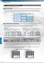
Power Management ICs (DC/DC Converter)<br />
New : Under Development :<br />
DC/DC Converters Lineup in order of Input Voltage and Function<br />
Major products are classified by input voltage and function. This chart does not include all products.<br />
40V<br />
1.2A output R1245x For PMOLED, General Use R1204xxxxB/C/E/F<br />
R1204xxxxA/D<br />
High voltage 2A output<br />
R1243x For white LED (External diode)<br />
R1204xxxxG/H<br />
20V<br />
Middle voltage<br />
6V<br />
Low voltage<br />
3A output<br />
18.5V, Reset Protection<br />
18.5V, Latch Protection<br />
600mA output<br />
600mA output,<br />
VOUT Ext.adjjustable<br />
600mA output, 6MHz<br />
1A output<br />
2A output<br />
1A dual output<br />
R1242S<br />
R1270S<br />
R1224N<br />
R1225N<br />
RP504x<br />
RP507K<br />
RP508K<br />
RP505K<br />
RP506K<br />
RP550K<br />
For white LED (External diode),<br />
4 strings<br />
For white LED (Internal diode)<br />
For white LED (External diode)<br />
For PMOLED, General Use<br />
For General Use<br />
For General Use<br />
For General Use,<br />
Synchronous Rectifier<br />
For General Use<br />
R1208K<br />
R1202xxxxD<br />
R1203x071B<br />
R1206N071B<br />
R1202xxxxA/B<br />
R1213K001B<br />
RP401x<br />
RP402x<br />
R1213K001A<br />
Step-up and Inverting<br />
Step-up and Charge pump<br />
Step-up, LDO and Amplifier<br />
Step-up and Inverting<br />
Step-up, LDO and VD<br />
R1283K<br />
R1290K<br />
R1293K<br />
R1286K<br />
RP600K<br />
Step-down Step-up Multi Power Supply<br />
High voltage Step-down DC/DC Converters Lineup<br />
These products are high voltage step-down DC/DC converters. These products include an under-voltage lockout circuit (UVLO), a soft-start circuit and a<br />
thermal shutdown circuit.<br />
The products highlighted in purple rows are major products that are shown in the "DC/DC Converters Lineup in order of Input Voltage and Function".<br />
• Products partially available for automotive applications. Products for automotive applications may not provide all specifications of products for<br />
consumer applications. Please refer to the "CAR ELECTRONICS PRODUCTS Catalog" for additional details.<br />
Product<br />
Name<br />
R1240x<br />
00xA<br />
00xB<br />
Version<br />
Control<br />
Input Voltage<br />
Range<br />
PWM 4.5V to 30.0V<br />
R1244N 001B PWM 4.5V to 30.0V<br />
R1245x<br />
R1243x<br />
R1242S<br />
R1270S<br />
00xA/C/E/G<br />
•<br />
00xB/D/F/H<br />
001A/C<br />
001B/D<br />
001A/C/E/G<br />
001B/D/F/H<br />
001A<br />
•<br />
001B<br />
PWM 4.5V to 30.0V<br />
PWM 4.5V to 30.0V<br />
PWM 5.0V to 30.0V<br />
PWM,<br />
PWM/VFM<br />
Auto Switching<br />
3.6V to 34.0V<br />
Output Voltage<br />
Range<br />
Ext. adjustable between<br />
0.8V and 15.0V<br />
Ext. adjustable between<br />
0.8V and 15.0V<br />
Ext. adjustable between<br />
0.8V and 27.6V<br />
(A to D)<br />
Ext. adjustable between<br />
0.8V and 18.0V<br />
Ext. adjustable between<br />
0.8V and 15.0V<br />
Ext. adjustable between<br />
0.8V and 28.0V<br />
(at 300kHz, VIN=34.0V)<br />
Output Protection<br />
Frequency<br />
Rectifier<br />
Current *1 Circuit<br />
Latch type<br />
±12mV 1.25MHz 1.2A<br />
Diode Rectifier<br />
Fold-back type<br />
VFB Voltage<br />
Accuracy<br />
Package<br />
SOT-23-6W *2<br />
DFN(PLP)2527-10<br />
±12mV 1.25MHz 1.2A Fold-back type Diode Rectifier SOT-23-6W *2<br />
±8mV<br />
±7mV<br />
±12mV<br />
±8mV<br />
330kHz (A/B)<br />
500kHz (C/D)<br />
1MHz (E/F)<br />
2.4MHz (G/H)<br />
330kHz (C/D)<br />
1MHz (A/B)<br />
330kHz (C/D)<br />
500kHz (E/F)<br />
1MHz (G/H)<br />
Ext. adjustable between<br />
330kHz to 1MHz (A/B)<br />
Ext. adjustable between<br />
300kHz to 2.4MHz<br />
(Built-in PLL)<br />
1.2A<br />
2A<br />
3A<br />
3A<br />
Latch type<br />
DFN(PLP)2020-8<br />
DFN2020-8<br />
Diode Rectifier<br />
*3<br />
SOT-23-6W<br />
Fold-back type<br />
HSOP-8E<br />
Latch type<br />
DFN(PLP)2527-10<br />
Diode Rectifier<br />
Fold-back type<br />
HSOP-8E<br />
Latch type Synchronous<br />
Rectifier<br />
HSOP-8E<br />
(with external<br />
Fold-back type low side transistor)<br />
Latch type<br />
Fold-back type<br />
Diode Rectifier<br />
HSOP-18P<br />
*1) This is an approximate value, because output current depends on conditions and external parts. *2) The pin-layout of R1240N and that of R1244N is upside down.<br />
*3) R1245L (DFN2020-8) : Only for automotive applications.<br />
Middle voltage Step-down DC/DC Controllers Lineup<br />
These products are middle voltage step-down DC/DC controllers with an external output transistor. These products include a soft-start circuit and an undervoltage<br />
lockout circuit (UVLO). (R1223N doesn't include a UVLO.)<br />
The products highlighted in green rows are major products that are shown in the "DC/DC Converters Lineup in order of Input Voltage and Function".<br />
<br />
Product<br />
Input Voltage Output Voltage Voltage<br />
Protection<br />
Version Control<br />
Frequency Output Tr. Output Current<br />
Name<br />
Range<br />
Range<br />
Accuracy *1 Circuit<br />
Package<br />
xx2A/B PWM/VFM Auto switching<br />
300kHz<br />
Latch type<br />
xx2C/D<br />
PWM<br />
(A/C/E/G)<br />
Depends on<br />
R1223N<br />
2.3V to 13.2V 1.5V to 5.0V ±2%<br />
External<br />
xx2E/F PWM/VFM Auto switching<br />
500kHz<br />
external MOSFET.<br />
(B/D/F/H)<br />
Reset type<br />
xx2G/H<br />
PWM<br />
SOT-23-5<br />
xx2E/F/L PWM/VFM Auto switching<br />
1.2V to 6.0V<br />
180kHz (L/M)<br />
xx2G/H/M<br />
Depends on<br />
R1224N<br />
2.3V to 18.5V<br />
±2% 300kHz (E/G) External<br />
PWM<br />
Ext. adjustable between<br />
external MOSFET.<br />
102G/H/M<br />
500kHz (F/H)<br />
1.0V to VIN<br />
Reset type SOT-23-5<br />
R1225N xx2C/D/K PWM 180kHz (J/K)<br />
Depends on<br />
2.3V to 18.5V 1.2V to 6.0V ±2% 300kHz (A/C) External<br />
xx2A/B/J PWM/VFM Auto switching<br />
external MOSFET.<br />
500kHz (B/D)<br />
Latch type SOT-23-6W<br />
*1) When the output voltage is adjusted by external resistors, the value means the feedback voltage accuracy.
2 0 1 3<br />
New : Under Development :<br />
Low voltage Step-down DC/DC Converters Lineup<br />
These products are low voltage step-down DC/DC converters with a synchronous rectifier. These products include an under-voltage lockout circuit (UVLO),<br />
a soft-start circuit and a latch type protection circuit. (RP507K and RP508K don't include a latch type protection circuit.)<br />
The products highlighted in pink rows are major products that are shown in the "DC/DC Converters Lineup in order of Input Voltage and Function".<br />
Product<br />
Name<br />
Version<br />
Control<br />
Forced PWM,<br />
PWM/VFM Auto Switching<br />
PWM/VFM Auto Switching<br />
Forced PWM<br />
Forced PWM,<br />
PWM/VFM Auto Switching<br />
Forced PWM,<br />
PWM/VFM Auto Switching<br />
MODE<br />
pin<br />
Input Voltage<br />
Range<br />
Output Voltage<br />
Range<br />
Voltage<br />
*1 Frequency<br />
Output<br />
Accuracy<br />
Current *2<br />
Thermal<br />
Shutdown<br />
Auto-<br />
Discharge<br />
Package<br />
RP500x<br />
xx1A PWM/VFM Auto Switching<br />
— WLCSP-6-P2<br />
xx2A<br />
PWM<br />
DFN1616-6<br />
— 2.55V to 5.5V 1.1V to 3.3V ±1.5% 1.2MHz 600mA —<br />
xx3A PWM/VFM Auto Switching<br />
DFN(PLP)1820-6<br />
SOT-23-6W<br />
xx4A<br />
PWM<br />
RP503x<br />
xx1A<br />
— DFN1616-6<br />
PWM/VFM Auto Switching — 2.5V to 5.5V 0.8V to 2.5V ±1.5% 2MHz 600mA —<br />
xx2A<br />
SOT-23-5<br />
RP507K 001B PWM/VFM Auto Switching — 2.3V to 5.5V<br />
Ext. adjustable between<br />
0.7V to 5.5V<br />
±9mV 2MHz 600mA DFN(PLP)1616-6D<br />
xx1A<br />
DFN(PLP)1216-6F<br />
DFN1616-6B<br />
RP504x<br />
xx1B<br />
—<br />
2.3V to 5.5V<br />
— 0.8V to 3.3V ±1.5% 2.25MHz 600mA —<br />
xx1C<br />
(VOUT≥1.0V)<br />
SOT-23-5<br />
RP508K<br />
RP502x<br />
R1232D<br />
RP501K<br />
RP505K<br />
RP506K<br />
• Dual Output<br />
xx1D<br />
xx1A<br />
xx1B<br />
xx1B<br />
xx2B<br />
xx3B<br />
xx4B<br />
RP550K Dual 001A<br />
PWM/VFM Auto Switching<br />
PWM<br />
PWM/VFM Auto Switching<br />
PWM<br />
2.3V to 5.5V 0.8V to 3.3V ±1.5% 6MHz 600mA<br />
— 2.5V to 5.5V 0.8V to 3.3V ±1.5% 3.3MHz 600mA —<br />
—<br />
—<br />
DFN(PLP)1216-6F<br />
DFN1616-6B<br />
DFN(PLP)1212-6<br />
WLCSP-6-P2<br />
DFN1616-6<br />
xx1A/B<br />
0.9V to 3.3V ±2% 1MHz<br />
(A/C)<br />
PWM — 2.6V to 5.5V<br />
Ext. adjustable between<br />
2.25MHz<br />
001C/D<br />
±16mV<br />
0.8V to VIN<br />
(B/D)<br />
1A — — SON-8<br />
xx1A<br />
PWM,<br />
—<br />
2.5V to 5.5V 1.0V to 3.3V ±1.5% 2.25MHz 1A —<br />
xx1B PWM/VFM Auto Switching<br />
DFN(PLP)2527-10<br />
xx1A<br />
2.3V to 5.5V<br />
—<br />
0.6V to 3.3V ±1.5%<br />
xx1B Forced PWM,<br />
(VOUT≥0.8V)<br />
2.25MHz 1A<br />
PWM/VFM Auto Switching<br />
Ext. adjustable between<br />
001C 2.3V to 5.5V ±9mV —<br />
0.8V to 3.3V<br />
DFN(PLP)2020-8<br />
xx1A/D<br />
0.8V to 3.3V (A/B)<br />
—<br />
±1.5%<br />
xx1B/E<br />
0.6V to 3.3V (D/E)<br />
1.2MHz<br />
2.5V to 5.5V<br />
Forced PWM,<br />
or Ext. adjustable between<br />
(D/E/F)<br />
001C<br />
2A<br />
PWM/VFM Auto Switching<br />
2.25MHz<br />
2.5V to 4.5V 0.8V to 3.8V<br />
±9mV (A/B/C)<br />
—<br />
Ext. adjustable between<br />
001F<br />
0.6V to 3.8V<br />
DFN(PLP)2527-10<br />
Forced PWM,<br />
PWM/VFM Auto Switching<br />
2.3V to 5.5V<br />
(VOUT≥0.8V)<br />
Ext. adjustable between<br />
0.6V to 3.3V<br />
*1) When the output voltage is adjusted by external resistors, the value means the feedback voltage accuracy.<br />
*2) This is an approximate value, because output current depends on conditions and external parts.<br />
±9mV 2.25MHz 1A×2 — DFN(PLP)2730-12<br />
10
Power Management ICs (DC/DC Converter)<br />
New : Under Development :<br />
Step-up DC/DC Converters Lineup (For white LED / For PMOLED and General use)<br />
These products are PWM step-up DC/DC converters, which are optimized to drive a white LEDs for background illumination or passive matrix OLED display<br />
with constant current. These products include an under-voltage lockout circuit (UVLO), and a soft-start circuit. These are also able to be used in a general<br />
step-up power supply.<br />
The products highlighted in yellow rows are major products that are shown in the "DC/DC Converters Lineup in order of Input Voltage and Function".<br />
Succeeding products are available for products highlighted in grey rows. We recommend the products shown in "Product Name".<br />
Rxxxx<br />
• For White LED<br />
Diode<br />
Internal<br />
External<br />
Product<br />
Name<br />
R1201N<br />
R1202x<br />
Version<br />
021/023<br />
Control<br />
Input Voltage<br />
Range<br />
Output Voltage<br />
Range<br />
VFB VFB Voltage<br />
Frequency<br />
Voltage Accuracy<br />
Lx Current<br />
Limit *1<br />
OVP Voltage<br />
(Typ.)<br />
9.5V<br />
Thermal<br />
Shutdown Shutdown High-speed<br />
Dimming<br />
Package<br />
031/033 Ext. adjustable<br />
1.8V to 5.5V<br />
1MHz<br />
14.0V<br />
041/043 (up to 20V)<br />
(0x1/2)<br />
PWM<br />
0.2V ±10mV<br />
700mA<br />
18.5V<br />
— — SOT-23-6<br />
1.2MHz<br />
051/053<br />
(0x3/4)<br />
20.6V<br />
Ext. adjustable<br />
052/054 1.8V to 4.5V<br />
21.6V<br />
(up to 21V)<br />
3xxD<br />
Ext. adjustable<br />
350mA 14.0V DFN1616-6B<br />
PWM 1.8V to 5.5V<br />
0.2V ±10mV 1.2MHz<br />
7xxD (up to 22.2V)<br />
700mA 23.0V<br />
TSOT-23-6<br />
8x1B<br />
Ext. adjustable 0.2V 350mA<br />
R1205L<br />
PWM 1.8V to 5.5V<br />
±10mV 1.2MHz<br />
8x1C (up to 24.2V) 0.4V<br />
700mA<br />
R1205N<br />
R1207N 8x3B PWM 1.8V to 5.5V Ext. adjustable<br />
350mA<br />
0.2V ±10mV 1.2MHz<br />
(up to 24.2V)<br />
700mA<br />
8x3B<br />
Ext. adjustable 0.2V 350mA<br />
R1207N<br />
PWM 1.8V to 5.5V<br />
±10mV 1.2MHz<br />
8x3C (up to 24.2V) 0.4V<br />
700mA<br />
25.0V — DFN1616-6B<br />
25.0V — TSOT-23-6 *2<br />
25.0V — TSOT-23-6 *2<br />
R1218x<br />
021A<br />
031A PWM 1.8V to 5.5V<br />
9.5V<br />
Ext. adjustable<br />
0.2V ±10mV 1.2MHz 700mA 14.0V — — — DFN(PLP)1820-6<br />
(up to 17V)<br />
SOT-23-6<br />
041A 18.5V<br />
R1203L 071B PWM 1.8V to 5.5V<br />
Ext. adjustable<br />
(up to 28.7V)<br />
0.2V ±10mV 1.2MHz 700mA 29.5V — — DFN1616-6B<br />
R1203N<br />
R1206N 071B PWM 1.8V to 5.5V Ext. adjustable<br />
(up to 28.7V)<br />
0.2V ±10mV 1.2MHz 700mA 29.5V — — SOT-23-6 *2<br />
R1206N 071B PWM 1.8V to 5.5V<br />
Ext. adjustable<br />
(up to 28.7V)<br />
0.2V ±10mV 1.2MHz 700mA 29.5V — — SOT-23-6 *2<br />
11xA/D<br />
1MHz<br />
23.0V<br />
21xA/D 0.2V<br />
(A)<br />
750kHz<br />
33.0V<br />
R1204x<br />
31xA/D Ext. adjustable<br />
(D)<br />
42.0V<br />
DFN(PLP)1820-6<br />
PWM 2.3V to 5.5V<br />
±10mV<br />
900mA<br />
—<br />
11xG/H<br />
(up to 40.2V)<br />
1MHz<br />
23.0V<br />
TSOT-23-6<br />
21xG/H 0.4V<br />
(G)<br />
750kHz<br />
33.0V<br />
31xG/H (H)<br />
42.0V<br />
R1218x<br />
052A<br />
23.0V<br />
062A PWM 1.8V to 5.5V<br />
Ext. adjustable<br />
(up to 30V)<br />
0.2V ±10mV 1.2MHz 700mA 27.5V<br />
072A 31.5V<br />
— — — DFN(PLP)1820-6<br />
SOT-23-6<br />
• For White LED (4 strings)<br />
Diode<br />
External<br />
Product<br />
Name<br />
R1208K<br />
Version<br />
Control<br />
Input Voltage<br />
Range<br />
Output Voltage<br />
Range<br />
LED<br />
Current<br />
(Max.)<br />
LED<br />
Current<br />
Accuracy<br />
Frequency<br />
Lx<br />
Current<br />
Limit *1<br />
OVP<br />
Voltage<br />
(Typ.)<br />
23.0V<br />
112A/B<br />
750kHz<br />
212A/B PWM 2.7V to 22.0V ±3%<br />
Ext. adjustable<br />
(up to 42V)<br />
80mA<br />
(4 strings)<br />
(A)<br />
450kHz<br />
2A 33.0V<br />
312A/B (B)<br />
43.5V<br />
*1) Lx current limit is different from output current.<br />
*2) The pin-layout of R1205N and that of R1207N is upside down. The pin-layout of R1203N and that of R1206N is upside down.<br />
Thermal<br />
High-speed<br />
Shutdown<br />
Shutdown Dimming<br />
Package<br />
— DFN(PLP)2730-12<br />
11
2 0 1 3<br />
• For PMOLED and General use<br />
Diode<br />
Internal<br />
External<br />
Product<br />
Name<br />
R1200x<br />
R1202x<br />
Version<br />
Control<br />
Input Voltage<br />
Range<br />
Output Voltage<br />
Range<br />
VFB VFB Voltage<br />
Frequency<br />
Voltage Accuracy<br />
Lx Current OVP Voltage<br />
Limit *1 (Typ.)<br />
001x<br />
17.0V<br />
002x PWM 2.3V to 5.5V<br />
Ext. adjustable<br />
(up to 20V)<br />
1.0V ±15mV 1.2MHz 700mA 19.0V<br />
003x 21.0V<br />
3xxA/B<br />
14.0V<br />
4xxA/B 17.0V<br />
5xxA/B PWM 2.3V to 5.5V<br />
Ext. adjustable<br />
350mA<br />
1.0V ±15mV 1.2MHz<br />
(up to 22.2V)<br />
700mA<br />
19.0V<br />
6xxA/B 21.0V<br />
Thermal<br />
Shutdown Shutdown<br />
—<br />
Auto-<br />
Discharge<br />
(A)<br />
(B) —<br />
(A)<br />
(B) —<br />
Package<br />
DFN1616-6<br />
DFN(PLP)1820-6<br />
SOT-23-6<br />
DFN1616-6B<br />
TSOT-23-6<br />
7xxA/B 23.0V<br />
R1205L 8xxA PWM 2.3V to 5.5V<br />
Ext. adjustable<br />
(up to 24.2V) 1.0V ±15mV 1.2MHz 350mA<br />
700mA<br />
25.0V — — DFN1616-6B<br />
R1205N<br />
Ext. adjustable<br />
8xxA PWM 2.3V to 5.5V<br />
R1207N (up to 24.2V) 1.0V ±15mV 1.2MHz 350mA<br />
700mA<br />
25.0V — — TSOT-23-6 *2<br />
R1207N 8x3A PWM 2.3V to 5.5V<br />
Ext. adjustable<br />
(up to 24.2V) 1.0V ±15mV 1.2MHz 350mA<br />
700mA<br />
25.0V — — TSOT-23-6 *2<br />
R1204x<br />
11xB/C/E/F PWM(B/E)<br />
1MHz<br />
23.0V<br />
PWM,<br />
Ext. adjustable<br />
PWM/VFM 2.3V to 5.5V<br />
(up to 40.2V) 1.0V ±15mV (B/C)<br />
21xB/C/E/F 900mA 33.0V<br />
— — DFN(PLP)1820-6<br />
750kHz<br />
TSOT-23-6<br />
Auto Switching<br />
31xB/C/E/F (E/F)<br />
(C/F)<br />
42.0V<br />
*1) Lx current limit is different from output current. *2) The pin-layout of R1205N and that of R1207N is upside down.<br />
Under Development :<br />
Step-up DC/DC Converters Lineup (General use)<br />
Thermal : Thermal shutdown circuit<br />
The products highlighted in orange rows are major products that are shown in the "DC/DC Converters Lineup in order of Input Voltage and Function".<br />
Product<br />
Name<br />
Version<br />
Control<br />
Input Voltage<br />
Range<br />
Output Voltage<br />
Range<br />
Voltage<br />
Frequency Output Lx Current<br />
Accuracy *1<br />
Tr. Limit *2<br />
RN5RK xx1x 0.75V to 8.0V Max. Internal<br />
VFM<br />
2.0V to 5.5V ±2.5%<br />
xx2A 0.7V to 8.0V 100kHz External<br />
R1210N<br />
R1213K<br />
RP400x<br />
RP401x<br />
RP402x<br />
xx1x<br />
0.9V to 8.0V<br />
100kHz<br />
Internal<br />
(A/C)<br />
PWM<br />
2.2V to 6.0V ±2.5%<br />
180kHz<br />
xx2x 0.8V to 8.0V<br />
(D)<br />
External<br />
001A<br />
001B<br />
xx1A<br />
xx1B<br />
PWM 2.3V to 5.5V<br />
PWM/VFM<br />
Auto Switching<br />
0.7V to 5.5V<br />
xx1C 1.2V to 5.5V<br />
Ext. adjustable<br />
between<br />
3.0V to 6.0V<br />
Ext. adjustable<br />
between<br />
6.0V to 15.0V<br />
1.8V to 5.0V<br />
or<br />
Ext. adjustable<br />
between<br />
1.8V to 5.0V<br />
(only DFN)<br />
Soft Start<br />
Protection<br />
Circuit<br />
Features, Remarks<br />
Package<br />
— — — SOT-23-5<br />
— *3 —<br />
±8mV 1MHz Internal 2.5A (Ext. adjustable)<br />
Latch type<br />
(xx1A) With frequency<br />
change-over circuit.<br />
(Output voltage range: 2.2V to 3.5V)<br />
(R1210Nxx2A doesn't exist.)<br />
Ext. phase compensation.<br />
Input to output path<br />
disconnected by external<br />
P-channel MOSFET controlled<br />
by FLAG pin.<br />
Built-in under-voltage lockout<br />
circuit. (UVLO)<br />
Thermal<br />
±2% 700kHz Internal 600mA *4 — Built-in Anti-ringing switch.<br />
SOT-23-5<br />
DFN(PLP)2730-12<br />
DFN(PLP)1820-6<br />
SOT-23-5<br />
xx1A PWM,<br />
Latch type Selectable PWM or PWM/VFM auto<br />
PWM/VFM<br />
1.8V to 5.5V<br />
DFN(PLP)1820-6<br />
xx1B Auto Switching<br />
— switching mode by MODE pin.<br />
PWM/VFM<br />
1.8V to 5.5V<br />
xx1C<br />
0.6V to 5.5V<br />
±2% 1.2MHz Internal 1A<br />
Auto Switching<br />
or<br />
*4 —<br />
Ext. adjustable<br />
DFN(PLP)1820-6<br />
between<br />
SOT-23-5<br />
xx1D PWM 1.8V to 5.5V<br />
—<br />
(only DFN)<br />
xx1A/B<br />
xx1C/D<br />
PWM,<br />
PWM/VFM<br />
Auto Switching<br />
PWM/VFM<br />
Auto Switching<br />
0.5V to 5.5V<br />
1.8V to 5.5V ±1.5%<br />
Ext. adjustable<br />
between ±15mV<br />
1.8V to 5.5V<br />
1.2MHz Internal 1.5A Latch type<br />
Synchronous Rectifier.<br />
Built-in Anti-ringing switch.<br />
Shutdown function (A/C)<br />
and Bypass function (B/D).<br />
Selectable PWM or PWM/VFM<br />
auto switching mode by MODE<br />
pin (A/B).<br />
DFN(PLP)2020-8<br />
1.8V to 5.5V ±1.5% Built-in Over-voltage lockout SOT-23-5<br />
circuit (UVLO), Over Voltage<br />
Protection Circuit (OVP).<br />
*1) When the output voltage is adjusted by external resistors, the value means the feedback voltage accuracy. *2) Lx current limit is different from output current.<br />
*3) A function used to detect sudden peaks in output voltage and to reduce overshoot/undershoot. *4) Will change according to the duty cycle.<br />
12
Power Management ICs (DC/DC Converter)<br />
DC/DC Converters Lineup for LCD / OLED / CCD<br />
New :<br />
Thermal : Thermal shutdown circuit Discharge : Auto-Discharge function Sequence : Power on sequence controllable<br />
These products are suitable for the power management of LCD, OLED and CCD. Many variations are available such as step-up DC/DC controller, stepup<br />
and step-down dual output converter and step-up and positive / negative charge pump triple output converter. These products include an under-voltage<br />
lockout circuit (UVLO), and a latch type protection circuit. The products with a built-in the sequence control circuit<br />
option are able to control a start-up sequence and a shutdown sequence.<br />
The products highlighted in light blue rows are major products that are shown in the "DC/DC Converters Lineup in order of Input Voltage and Function".<br />
• Products partially available for automotive applications. Products for automotive applications may not provide all specifications of products for<br />
consumer applications. Please refer to the "CAR ELECTRONICS PRODUCTS Catalog" for additional details.<br />
• Step-up<br />
Product<br />
Name<br />
Control<br />
Input Voltage<br />
Range<br />
Output Voltage<br />
Range<br />
R1211x • PWM 2.5V to 6.0V Ext. adjustable ±15mV<br />
R1212D PWM 2.2V to 5.5V Ext. adjustable ±15mV<br />
R1215D PWM 1.8V to 5.5V Ext. adjustable ±15mV<br />
• Step-up and Inverting<br />
Product<br />
Name<br />
R1283K<br />
R1286K<br />
0xxx<br />
1xxx<br />
001B<br />
Input Voltage Output Voltage<br />
Control<br />
Range Range<br />
PWM (Step-up)<br />
Ext. adjustable<br />
up to 20V<br />
2.5V to 5.5V<br />
Ext. adjustable<br />
PWM (Inverting)<br />
up to VDD-20V<br />
PWM (Step-up)<br />
Voltage<br />
Frequency Output Lx Current<br />
Accuracy *1 Tr.<br />
300kHz<br />
700kHz<br />
External —<br />
300kHz<br />
700kHz External —<br />
1.4MHz<br />
700kHz<br />
1.4MHz<br />
External —<br />
4.6V to 5.8V ±0.9%<br />
Voltage<br />
Frequency Output Lx Current<br />
Accuracy *1<br />
Tr. Limit *2<br />
±1.5% 300kHz 1.5A<br />
700kHz Internal<br />
±25mV 1.4MHz 1.5A<br />
PWM (Inverting) -2.0V to -6.0V ±70mV 1.5A<br />
PWM (Step-up) 4.6V to 5.8V ±0.9% 1.1A<br />
PWM (Inverting)<br />
2.3V to 4.8V<br />
-2.0V to -6.0V ±70mV<br />
1.75MHz Internal<br />
1.8A<br />
PWM (Step-up)<br />
PWM (Inverting)<br />
• Step-up and Charge pump<br />
Ext. adjustable<br />
between<br />
4.6V to 5.8V<br />
Ext. adjustable<br />
between<br />
-2.0V to -6.0V<br />
±15mV<br />
Limit *2 Soft Start Features, Remarks Package<br />
(A/C) Ext. phase compensation.<br />
SON-6<br />
(B/D) Int. phase compensation. With stand-by. SOT-23-6W<br />
1A<br />
1A<br />
±25mV 1.5A<br />
(Ext. adjustable)<br />
(Ext. adjustable)<br />
Soft<br />
Start<br />
Timer Latch<br />
Delay Time<br />
50ms<br />
16ms<br />
40ms<br />
16ms<br />
Ext. phase compensation.<br />
Maxduty Ext. adjustable.<br />
Ext. phase compensation.<br />
Maxduty Ext. adjustable.<br />
Features, Remarks<br />
Discharge (Inverting output only)<br />
Sequence<br />
Synchronous Rectifier.<br />
Inverting output can be dynamically<br />
changed by single wire control.<br />
Sequence Discharge Thermal<br />
Synchronous Rectifier.<br />
Sequence Discharge Thermal<br />
SON-8<br />
SON-8<br />
Package<br />
DFN(PLP)2730-12<br />
DFN(PLP)2730-12<br />
Product<br />
Input Voltage Output Voltage Voltage<br />
Output Lx Current<br />
Control<br />
Frequency<br />
Soft Start Features, Remarks Package<br />
Name<br />
Range Range Accuracy *1<br />
Tr. Limit *2<br />
PWM (Step-up)<br />
±1.5% Ext. adjustable<br />
2A<br />
The charge pump operates at<br />
R1290K • Charge pump (Positive) 2.0V to 5.5V Ext. adjustable ±25mV between Internal —<br />
1/4th operating frequency. QFN0404-24<br />
180kHz to 1.4MHz<br />
(Ext. adjustable)<br />
Charge pump (Negative) ±30mV —<br />
Sequence<br />
Ext. adjustable<br />
PWM (Step-up)<br />
±15mV<br />
Internal 2A<br />
DC/DC output with noise<br />
up to 16.0V<br />
2.2V to 5.5V<br />
Ext. adjustable<br />
reduction function.<br />
R1293K<br />
between<br />
IOUT=<br />
VCOM amplifier 1 channel, QFN(PLP)0404-32<br />
LDO 1.8V to 2.5V ±1% Internal<br />
300kHz to 1MHz 350mA<br />
(Ext. adjustable) GAMMA amplifier 6 channel.<br />
Amplifier 5.0V to 16.0V — — — —<br />
Thermal<br />
*1) When the output voltage is adjusted by external resistors, the value means the feedback voltage accuracy. *2) Lx current limit is different from output current.<br />
Step-up DC/DC Converters with VD and VR Lineup<br />
The products highlighted in blue rows are major products that shown in the "DC/DC Converters Lineup in order of Input Voltage and Function". Thermal : Thermal shutdown circuit<br />
13<br />
Product<br />
Name<br />
RP600K0xxA<br />
RP600K0xxB<br />
RP600K2xxC<br />
RP600K1xxD<br />
Product<br />
Name<br />
RP600K0xxA<br />
Control<br />
PWM,<br />
PWM/VFM<br />
Auto switching<br />
Output<br />
Current<br />
500mA<br />
Input Voltage<br />
Range<br />
0.8V to 5.5V<br />
Input Voltage<br />
Range<br />
DC/DC Part<br />
Output Voltage<br />
CE Frequency Output<br />
Range *1<br />
Tr.<br />
CE<br />
2.3V to 5.5V<br />
(Accuracy: ±2%)<br />
CE1<br />
CE<br />
Ext. adjustable 1.2MHz Internal 1.4A —<br />
between<br />
CE<br />
2.3V and 5.5V<br />
(Accuracy: ±12mV)<br />
Output Voltage<br />
Range<br />
LDO Part<br />
CE ECO Function Input<br />
CE<br />
Fast response mode only<br />
Lx Current<br />
Limit *2 UVLO Soft<br />
Start<br />
DC/DC<br />
output<br />
Operating<br />
Voltage Range<br />
Remarks<br />
Selectable PWM or PWM/VFM<br />
auto switching mode by<br />
MODE pin.<br />
Thermal (Except C)<br />
VD Part<br />
Detector<br />
Threshold Range<br />
Output<br />
Delay Time<br />
Package<br />
DFN(PLP)2527-10<br />
Hysteresis<br />
Range<br />
5%<br />
In DC/DC enabled<br />
RP600K0xxB 300mA CE2 Fast response mode<br />
VIN 1.0V to 4.5V<br />
5%<br />
1.5V to 5.0V<br />
2.0V to 5.5V In DC/DC disabled<br />
0.8V to 5.5V (Accuracy: ±2%)<br />
(Accuracy: ±1%) LDO mode selectable by MODE pin<br />
Monitor VSENSE<br />
RP600K2xxC 150mA — between Automatic mode shift and DC/DC<br />
—<br />
Fast response mode.<br />
output<br />
RP600K1xxD 500mA CE Fast response mode only 5%<br />
*1) When the output voltage is adjusted by external resistors, the value means the feedback voltage accuracy. *2) Lx current limit is different from output current.<br />
30% to 80%<br />
(10% steps)
2 0 1 3<br />
• RP600K Block Diagrams<br />
RP600K0xxA<br />
RP600K0xxB<br />
IN<br />
CE<br />
VIN<br />
CE<br />
Step-up<br />
DC/DC<br />
Lx<br />
VOUT1<br />
Diode<br />
OUT1<br />
IN<br />
CE1(DC/DC CE)<br />
VIN<br />
CE1<br />
Step-up<br />
DC/DC<br />
Lx<br />
VOUT1<br />
Diode<br />
OUT1<br />
MODE<br />
MODE<br />
500mA<br />
LDO<br />
VOUT2<br />
OUT2<br />
CE2(LDO CE)<br />
MODE<br />
CE2<br />
MODE<br />
300mA<br />
EDO LDO<br />
VOUT2<br />
OUT2<br />
VD SENSE<br />
VSENSE<br />
Voltage<br />
Detector<br />
VDOUT<br />
VD OUT<br />
VD SENSE<br />
VSENSE<br />
Voltage<br />
Detector<br />
VDOUT<br />
VD OUT<br />
GND<br />
GND<br />
• DC/DC output is connected to the LDO input.<br />
• LDO output (OUT2) operates as step-up and step-down power supply.<br />
RP600K2xxC<br />
• Both DC/DC and LDO use VIN as input.<br />
• RP600K0xxB is configured as a step-up DC/DC and LDO, a dual output power supply.<br />
RP600K1xxD<br />
IN<br />
VIN<br />
CE<br />
Step-up<br />
DC/DC<br />
Lx<br />
VOUT1<br />
Diode<br />
IN<br />
CE<br />
VIN<br />
CE<br />
Step-up<br />
DC/DC<br />
Lx<br />
VOUT1<br />
Diode<br />
OUT1<br />
MODE<br />
MODE<br />
150mA<br />
ECO LDO<br />
VOUT2<br />
OUT<br />
MODE<br />
MODE<br />
500mA<br />
LDO<br />
VFB<br />
VOUT2<br />
OUT2<br />
VDOUT<br />
Voltage<br />
Detector<br />
VSENSE<br />
VD SENSE<br />
VSENSE<br />
Voltage<br />
Detector<br />
VDOUT<br />
VD OUT<br />
GND<br />
GND<br />
• DC/DC output is connected to the LDO input.<br />
• Initially the DC/DC starts-up and charges a large output capacitor.<br />
When fully charged above the threshold of the VD, the DC/DC will be<br />
disabled. The LDO consumes charge from the capacitor and provides<br />
a stable output. As soon the charge drops below the threshold of the<br />
VD, the DC/DC is enabled again. This sequence is repeating.<br />
• RP600K2xxC operates as ultra low power consumption step-up and<br />
step-down power supply.<br />
• DC/DC output is connected to the LDO input.<br />
• DC/DC output voltage is adjustable by external resistors.<br />
• LDO output (OUT2) operates as step-up and step-down power supply.<br />
Step-down DC/DC Converters with VD and VR Lineup<br />
Product<br />
Input Voltage Output Voltage Voltage<br />
Control<br />
Name<br />
Range<br />
Range Accuracy Frequency Output Output<br />
UVLO Soft Protection<br />
Features, Remarks<br />
Tr. Current *1 Start Circuit<br />
Package<br />
R5220x PWM 2.8V to 5.5V 1.0V to 3.3V ±2% 1.2MHz Internal<br />
400mA<br />
Synchronous Rectifier.<br />
(at DC/DC)<br />
DFN(PLP)2514-6<br />
Latch type Built-in DC/DC and VR<br />
50mA<br />
SON-6<br />
alternative circuit.<br />
(at VR)<br />
800mA<br />
RP901K<br />
(A/B/C)<br />
1.2V to 1.8V (DC/DC) ±2%<br />
PWM,<br />
900mA<br />
Synchronous Rectifier.<br />
PWM/VFM 4.5V to 5.5V<br />
1.2MHz Internal (D)<br />
Built-in VD and VR.<br />
Reset type<br />
For DVD drive.<br />
Auto switching<br />
2.5V to 3.3V (VR) ±1% 600mA<br />
Thermal<br />
DFN(PLP)2527-10<br />
2.0V to 3.0V(VD)(A)<br />
3.0V to 5.0V(VD)(B/C/D)<br />
±2% —<br />
1.2V to 3.3V (DC/DC1) ±2%<br />
Synchronous Rectifier.<br />
Built-in Bypass switch.<br />
RP904Z<br />
PWM/VFM<br />
Manual<br />
switching<br />
2.5V to 5.5V<br />
1.0V to 1.5V (DC/DC2) ±30mV<br />
*1) This is an approximate value, because the output current depends on conditions and external parts.<br />
2MHz Internal 1A Latch type<br />
Output Voltage selectable<br />
from DC/DC1 or DC/DC2.<br />
WLCSP-11-P2<br />
14
Power Management ICs (Li-ion/polymer Battery Protection ICs)<br />
<strong>Ricoh</strong>'s Li-ion/polymer battery protection ICs have been released to the market since 1995, when the Li-ion rechargeable batteries became<br />
available. <strong>Ricoh</strong> has nearly 20 years of experience developing these products. These protection ICs protect batteries provide features like<br />
over-charge/discharge voltage, excess charge/discharge current and short circuit.<br />
<strong>Ricoh</strong> has a wide product portfolio of 1cell protection ICs for smartphones and tablets, 2cell protection ICs for DSLR and portable DVD<br />
players, multi cell protection ICs for electrical power tools and E-bike and 2nd protection ICs for notebook PCs and electrical power tools.<br />
1cell Li-ion/polymer Battery Protection IC Products Lineup<br />
<strong>Ricoh</strong>'s 1cell Li-ion/polymer battery protection ICs have a high detection accuracy. Especially R5470K/R5471K Series have an ultra high accuracy overcharge<br />
detection of ±10mV in a temperatutre range from 0°C to 50°C. R5480K Series have an ultra high accuracy excess discharge current detection of<br />
±15% (±4.5mV to 7.2mV).<br />
Product Name R5400N R5402N<br />
R5403x R5470K R5475N<br />
R5405x R5471K R5478N<br />
R5472x R5480K<br />
Supply Current Typ. 3.5μA or 4.0μA 4.0μA 3.0μA 4.0μA <br />
Standby Current Max. 0.1μA 0.1μA or 2.0μA 0.1μA 0.1μA or 2.0μA 0.1μA <br />
Detector Threshold Range<br />
(Accuracy)<br />
4.0V to 4.5V<br />
(±25mV)<br />
<br />
<br />
Over-charge<br />
4.1V to 4.5V *1<br />
(±10mV)<br />
4.2V to 4.5V,<br />
3.65V, 3.9V<br />
(±25mV)<br />
4.1V to 4.5V<br />
(±20mV)<br />
Output Delay Time Typ. 275ms or 1.1s 250ms or 1.0s 1.0s <br />
Protection<br />
Latch<br />
Latch<br />
Latch<br />
<br />
Latch<br />
or Auto release<br />
or Auto release<br />
Latch<br />
<br />
Over-discharge<br />
Detector Threshold Range 2.0V to 3.0V<br />
1.9V to 3.0V 2.1V to 3.0V<br />
<br />
(Accuracy)<br />
(±2.5%)<br />
(±2.5%)<br />
(±35mV)<br />
<br />
Output Delay Time Typ. 20ms <br />
Protection<br />
Latch<br />
Latch<br />
Latch<br />
<br />
Latch<br />
or Auto release<br />
or Auto release<br />
Latch<br />
<br />
Excess discharge current<br />
0.050V to 0.080V<br />
Detector Threshold Range 0.05V to 0.20V<br />
0.05V to 0.13V 0.05V to 0.20V (±10mV)<br />
<br />
<br />
(Accuracy)<br />
(±15mV)<br />
(±10mV)<br />
(±15mV) 0.081V to 0.100V<br />
(±15mV)<br />
<br />
0.030V to 0.048V<br />
(±15%)<br />
Output Delay Time Typ. 12ms 6ms or 12ms 6ms or 12ms or 16ms 12ms 6ms or 12ms 12ms <br />
Excess charge current<br />
-0.100V to -0.081V<br />
Detector Threshold Range<br />
-0.1V -0.2V to -0.05V -0.15V to -0.05V<br />
(±15mV)<br />
—<br />
—<br />
(Accuracy)<br />
(±30mV)<br />
(±30mV)<br />
(±20mV)<br />
-0.080V to -0.050V<br />
(±10mV)<br />
-0.030V to -0.020V<br />
(±15%)<br />
Output Delay Time Typ. — 8ms or 16ms 8ms or 16ms 16ms — 16ms <br />
Short Protection<br />
Detector Threshold Typ. 1.3V 0.8V 0.8V 0.6V 0.75V 0.5V 0.18V or 0.5V<br />
Output Delay Time Typ. 300μs 200μs or 300μs 200μs or 300μs or 400μs 250μs 200μs or 300μs 250μs <br />
0V charge Acceptable Prohibited Selectable Prohibited <br />
Remarks<br />
High precision ±10mV<br />
Excess current sensing<br />
by external resistor with RSENS pin.<br />
SOT-23-5 SOT-23-6 R5403x Series R5470K Series R5475N Series DFN(PLP)1414-6 DFN(PLP)1414-6<br />
DFN(PLP)1820-6 DFN(PLP)2114-4B SOT-23-5<br />
DFN1414-6<br />
SOT-23-5<br />
Package<br />
R5405x Series<br />
DFN(PLP)1616-6<br />
DFN1814-6<br />
SOT-23-6<br />
R5471K Series R5478N Series<br />
DFN(PLP)1616-6B SOT-23-6<br />
*1) Topt=0°C to 50°C, Considering of variation in parameters.<br />
We compensate for these characteristics related to temperature by laser-trimming, however, these specifications are guaranteed by design.<br />
• TYPICAL APPLICATION<br />
Battery Pack<br />
+<br />
New Package :<br />
R1<br />
330Ω<br />
C1<br />
0.1µF<br />
VDD<br />
R5480K<br />
V-<br />
VSS<br />
RSENS DOUT COUT<br />
R3<br />
5~10mΩ<br />
R2<br />
1kΩ<br />
–<br />
15<br />
RSENS: Over-current detector input pin<br />
Improved current sense accuracy is possible regardless of the MOSFET On-Resistance,<br />
even if considering the temperature characteristics by external resistor R3.<br />
(Excess current threshold of R5480K is ±15% (±4.5mV) at detector threshold 0.030V)<br />
*) Products built-in the RSENS pin: R5472K, R5480K
2 0 1 3<br />
2cell Li-ion/polymer Battery Protection IC Products Lineup<br />
<strong>Ricoh</strong>'s 2cell Li-ion/polymer battery protection ICs have a high accuracy. Especially R5461K and R5464K Series have an ultra high accuracy over-charge<br />
detection of +10mV and -15mV in a temperature range from 0°C to 50°C.<br />
Product Name R5460x R5461K R5462K R5463K R5464K<br />
Supply Current Typ. 4.0μA 4.0μA or 5.0μA 4.0μA 5.0μA or 6.0μA<br />
Standby Current Max. 0.1μA or 2.0μA 0.1μA 0.1μA or 2.0μA 0.1μA <br />
Over-charge<br />
Detector Threshold Range<br />
(Accuracy)<br />
4.2V to 4.5V<br />
or<br />
3.5V to 4.0V<br />
(±25mV)<br />
3.60V to 4.35V *1<br />
(+10mV/-15mV)<br />
3.65V to 4.32V *1<br />
(±10mV)<br />
3.65V to 4.32V<br />
(±20mV)<br />
4.0V to 4.3V *1<br />
(+10mV/-15mV)<br />
Output Delay Time Typ. 1.0s <br />
Protection Auto release <br />
Over-discharge<br />
Detector Threshold Range 2.0V to 3.0V<br />
2.0V to 3.2V<br />
2.0V to 3.0V<br />
<br />
<br />
(Accuracy)<br />
(±2.5%)<br />
(±2.5%)<br />
(±50mV)<br />
Output Delay Time Typ. 128ms <br />
Protection<br />
Latch<br />
Latch<br />
Latch<br />
or Auto release<br />
or Auto release<br />
Latch<br />
<br />
Excess discharge current<br />
Detector Threshold Range<br />
(Accuracy)<br />
0.05V to 0.20V<br />
(±15mV)<br />
0.05V to 0.24V<br />
(±15mV)<br />
0.05V to 0.20V<br />
(±10mV)<br />
0.05V to 0.20V<br />
(±10mV)<br />
or<br />
0.20V to 0.40V<br />
(±10%)<br />
0.05V to 0.24V<br />
(±15mV)<br />
Output Delay Time Typ. 12ms 12ms or 24ms 12ms 12ms or 16ms<br />
Excess charge current<br />
-0.1V<br />
(±30mV)<br />
or<br />
Detector Threshold Range<br />
-0.2V<br />
-0.22V to -0.1V<br />
-0.2V to -0.1V<br />
-0.22V to -0.1V<br />
<br />
(Accuracy)<br />
(±30mV)<br />
(±30mV)<br />
(±20mV)<br />
(±20mV)<br />
or<br />
-0.4V<br />
(±40mV)<br />
Output Delay Time Typ. 8ms <br />
Short Protection<br />
Detector Threshold Typ. 1.0V <br />
Output Delay Time Typ. 300μs <br />
0V charge Acceptable Selectable Prohibited Selectable<br />
Remarks with Alarm function High precision with Alarm function<br />
Package<br />
DFN(PLP)1820-6 DFN(PLP)2527-10 DFN(PLP)1820-6B DFN(PLP)1820-6B DFN(PLP)2527-10<br />
SOT-23-6<br />
*1) Topt=0°C to 50°C, Considering of variation in parameters.<br />
We compensate for this characteristics related to temperature by laser-trimming, however, these specifications are guaranteed by design.<br />
• TYPICAL APPLICATION<br />
Battery Pack<br />
• Alarm Function<br />
Voltage<br />
+<br />
R1 330Ω R5 330Ω<br />
C1 0.1µF<br />
VDD<br />
R2 330Ω<br />
VC<br />
C2 0.1µF<br />
Ps<br />
R5464K<br />
VSS<br />
DOUT<br />
TIN<br />
RIN<br />
AOUT ∗<br />
COUT<br />
V-<br />
T1<br />
R4<br />
R3<br />
470kΩ<br />
150kΩ<br />
1kΩ<br />
R6<br />
to Charger<br />
Alarm Output<br />
510kΩ<br />
Alarm detect voltage<br />
VALML<br />
at normal temperature<br />
Alarm detect voltage<br />
at high temperature<br />
VALMH<br />
Alarm On<br />
at normal temperature<br />
Alarm Off<br />
45°C<br />
Alarm On<br />
at high temperature<br />
Temperature<br />
TIN: External thermistor connection pin.<br />
RIN: External resistor connection pin.<br />
Ps: P-channel source pin for over-charge alarm output *<br />
*) Alarm output pin (AOUT) is a P-channel open drain output.<br />
In the R5464K, the source of AOUT is Ps pin, not VDD pin. Therefore, the<br />
external pull-down resistor, R6 does not have an impact on the drop out<br />
between a plus terminal of a battery pack and a VDD pin. Thus, R6 value<br />
range is wide enough to choose.<br />
–<br />
When cell 1 voltage or cell 2 voltage exceeds the alarm threshold voltage<br />
(VALML), an alarm signal will be present at the AOUT pin. If the detection<br />
temperature of thermistor exceeds 45°C, the alarm detect voltage threshold<br />
changes to VALMH.<br />
(The detection temperature can be changed)<br />
*) Products with alarm output controlled by an external thermistor.:<br />
R5461K, R5464K<br />
16
Power Management ICs (Li-ion/polymer Battery Protection ICs)<br />
Multi cell Li-ion/polymer Battery Protection IC Products Lineup<br />
<strong>Ricoh</strong>'s multi cell Li-ion/polymer battery protection ICs have several advanced features such as Cell Balance Function, Cascade Connection and Breaking Wire Detection.<br />
Product Name R5431V R5432V R5433V<br />
Supply Current Typ. 12.0μA 18.0μA 8.0μA<br />
Standby Current Max. 12.0μA — —<br />
Over-charge<br />
Detector Threshold Range<br />
3.6V to 4.5V<br />
(Accuracy)<br />
(±25mV)<br />
<br />
<br />
Output Delay Time Typ. 1.0s <br />
Protection Auto Release <br />
Over-discharge<br />
Detector Threshold Range<br />
2.0V to 3.0V<br />
(Accuracy)<br />
(±2.5%)<br />
<br />
<br />
Output Delay Time Typ. 128ms or 1.2s Settable by C1 <br />
Protection Auto Release <br />
Excess discharge current<br />
VD3-1 VDD-0.2V (±20mV)<br />
VD3-1 0.05V to 0.3V (±20mV)<br />
Detector Threshold Range<br />
(Accuracy)<br />
VD3-2 VDD-0.6V (±100mV)<br />
VD3-2 0.6V (±100mV) or 0.3V (±55mV)<br />
Output Delay Time Typ.<br />
tVD3-1 12ms or 1.0s<br />
tVD3-1 Settable by C2<br />
tVD3-2 2ms or 10ms<br />
tVD3-2 Settable by C2<br />
—<br />
Excess charge current<br />
Detector Threshold<br />
VD4 VDD+0.2V<br />
-0.05V -0.1V -0.2V -0.4V<br />
or<br />
or<br />
or<br />
(Accuracy)<br />
(±30mV)<br />
(±30mV) (±30mV) (±30mV) (±40mV)<br />
—<br />
Output Delay Time Typ. 8ms —<br />
Short Protection<br />
Detector Threshold VDD-1.2V 0.5V or 0.75V or 1.0V —<br />
Output Delay Time Typ. 300μs —<br />
0V charge Prohibited Acceptable <br />
Remarks<br />
For 3 to 4cell protection.<br />
High side protection FET.<br />
For 3 to 5cell or more protection. (IC cascadable *1 )<br />
Built-in Cell Balance Function.<br />
Built-in Breaking Wire Detection.<br />
—<br />
Control over-charge and over-discharge<br />
by output signal to MCU.<br />
(Signal Output type)<br />
Built-in Breaking Wire Detection.<br />
Package SSOP-16 SSOP-24 SSOP-16<br />
*1) 6 Cell, 8 Cell, 10 Cell protection or other/higher cell combinations possible by connecting multiple R5432V ICs in cascade.<br />
• TYPICAL APPLICATION<br />
Battery Pack<br />
Enlarged Figure<br />
Battery Pack<br />
Enlarged<br />
RVC1<br />
CVDD<br />
RVDD<br />
VC1 VDD<br />
RVDD<br />
Cell1<br />
Cell2<br />
ZD1<br />
Cell3<br />
Cell4<br />
Cell5<br />
RCB1<br />
RVC2<br />
RCB2<br />
RVC3<br />
RCB3<br />
RVC4<br />
RCB4<br />
RVC5<br />
RCB5<br />
CVC1<br />
CVC2<br />
CVC3<br />
CVC4<br />
CVC5<br />
CB1<br />
VC2<br />
CB2<br />
R5432V<br />
VC3<br />
CTLD<br />
CB3<br />
CTLC<br />
VC4 SEL2<br />
SEL1<br />
CB4<br />
VMP<br />
VC5 COUT<br />
DRAIN<br />
CB5 DOUT<br />
SENS<br />
VSS<br />
CT1 CT2 CTLT<br />
RSE<br />
VSS<br />
VSS<br />
RCO1<br />
RCO2<br />
RVMP<br />
Cell1<br />
RCB1<br />
RVC1<br />
ON<br />
Bypass Current<br />
RVC2<br />
CVDD<br />
CVC1<br />
VC1<br />
VC1 VDD<br />
CB1 "H"<br />
R5432V<br />
VC2<br />
CT1<br />
CT2<br />
CTLT<br />
RSENS<br />
RDRAIN<br />
• Cell Balance Operation<br />
Over-charge<br />
threshold<br />
Cell balance<br />
threshold<br />
Cell balance<br />
released threshold<br />
Voltage<br />
<br />
Charge<br />
Cell<br />
Voltage<br />
<br />
Charge<br />
Bypass Current Bypass Current Bypass Current<br />
Cell<br />
Voltage<br />
<br />
Cell Balance Operation<br />
Cell<br />
Voltage<br />
<br />
Cell<br />
Voltage<br />
<br />
Cell<br />
Voltage<br />
• Breaking Wire Detection<br />
In case of using a battery pack in electric power tools<br />
exposed to heavy vibrations, there is a risk that the protection<br />
circuit fails due to a breaking wire condition between battery<br />
cells and protection circuit board.<br />
The Breaking Wire Detection circuit performs a test at<br />
fixed intervals, depending on the capacitance connected to<br />
CTLT pin. When a breaking wire event occurs, it results in<br />
interrupting the charge or discharge condition.<br />
• Cascade Connection<br />
Multi cell Li-ion/polymer battery protection ICs can protect<br />
over 6cells by cascade connection.<br />
17<br />
When a cell voltage is lower than the cell balance threshold, a cell is charged.<br />
When a cell voltage becomes higher than the cell balance threshold, CB1 pin becomes "H" and<br />
N-channel transistor turns on, and then the cell balance operation starts. Then a bypass current<br />
flows to the direction of a arrow and a charge current becomes suppressed by the bypass current.<br />
When a cell voltage reaches to the over-charge threshold, cell charging stops after the output delay time.<br />
If charging to a cell stops, the cell balance operation continues until a cell voltage<br />
becomes lower than the cell balance released threshold. The bypass current continues to<br />
flow decreasing the cell voltage.<br />
When a cell voltage reaches to the cell balance released voltage, CB1 pin becomes "L"<br />
and N-channel transistor turns off, and then cell balance operation stops.<br />
Time<br />
Imaginary Figure<br />
COUT<br />
CTLC<br />
R5432V<br />
R5432V<br />
COUT<br />
DOUT<br />
CTLD DOUT<br />
VC1 VSS VC1 VSS
2 0 1 3<br />
Li-ion/polymer Battery 2nd Protection IC Products Lineup<br />
<strong>Ricoh</strong>'s Li-ion/polymer battery 2nd protection ICs support over-charge voltage protection only. These are suitable from 2cell to 5cell battery pack.<br />
Product Name R5434D R5435x<br />
Supply Current Typ. 3.0μA 3.0μA<br />
Standby Current Max. — 0.1μA<br />
Over-charge<br />
Detector Threshold<br />
(Accuracy)<br />
3.6V to 4.6V<br />
(±25mV)<br />
4.10V to 4.55V<br />
(±20mV)<br />
Output Delay Time Typ. 1.5s 2.0s or 4.0s or 6.0s<br />
COUT Output "H" Voltage Typ. 3.7V 4.7V<br />
Shutdown Detector Threshold Typ. — 3.5V<br />
Remarks 2 to 5cell 2 to 3cell<br />
Package<br />
SON-8<br />
DFN(PLP)1616-6<br />
TSOT-23-6<br />
• TYPICAL APPLICATION<br />
Battery Pack<br />
Self Control Protector<br />
RVDD<br />
100Ω<br />
+<br />
CVDD<br />
0.1µF<br />
Cell1<br />
Cell2<br />
Cell3<br />
R1<br />
1kΩ<br />
R2<br />
1kΩ<br />
R3<br />
1kΩ<br />
C1<br />
C2<br />
C3<br />
0.1µF<br />
0.1µF<br />
0.1µF<br />
VC1<br />
VC2<br />
VC3<br />
VDD<br />
R 5435x<br />
COUT<br />
VSS<br />
–<br />
*) When using as a 2cell protection IC, please short VC3 pin and VSS pin.<br />
Please contact to Dexerials Corporation about Self Control Protector.<br />
18
Power Management ICs (Package Information)<br />
For more details, please refer to the Package Information in the <strong>Ricoh</strong> Web site.<br />
• WLCSP<br />
Halogen<br />
Free<br />
Bottom<br />
View<br />
Dimensions<br />
Power Dissipation *<br />
in Standard condition<br />
Taping Quantity/<br />
Direction Reel<br />
Pin Symbol Package<br />
Actual Size<br />
Others<br />
Body Mount Area Thickness Pitch Remarks Tjmax=125°C Tjmax=150°C<br />
4 Z WLCSP-4-P2 H/F 0.79×0.79 0.79×0.79 0.48 0.5 φ0.16 530mW 662mW TR 5,000 R1183Z<br />
RP102Z<br />
4 Z WLCSP-4-P5 H/F 0.69×0.69 0.69×0.69 0.48 0.4 φ0.16 278mW 348mW TR 5,000<br />
RP106Z<br />
RP107Z<br />
RP200Z<br />
RP201Z<br />
4 Z WLCSP-4-P7 H/F 0.69×0.69 0.69×0.69 0.36 0.4 φ0.16 278mW — TR 5,000 RP116Z<br />
6 Z WLCSP-6-P2 H/F 1.29×0.87 1.29×0.87 0.48 0.5 φ0.16 650mW — E2 5,000 RP500Z<br />
RP502Z<br />
9 Z WLCSP-9-P1 H/F 1.27×1.27 1.27×1.27 0.64 0.4 φ0.26 1190mW — E2 5,000 R5528Z<br />
11 Z WLCSP-11-P2 H/F 2.37×1.47 2.37×1.47 0.78 0.5 φ0.16 1000mW — E2 4,000 RP904Z<br />
• DFN(PLP)<br />
Pin Symbol Package<br />
Halogen<br />
Free<br />
Actual Size<br />
Bottom<br />
View<br />
New : Under Development : Halogen Free : H/F<br />
Power Dissipation *<br />
Dimensions<br />
in Standard condition<br />
(in High Wattage condition)<br />
Body Mount Area Thickness Pitch Tjmax=125°C Tjmax=150°C<br />
4 K DFN(PLP)0808-4 H/F 0.8×0.8 0.8×0.8 0.4 0.48 286mW 358mW TR 10,000 —<br />
4 K DFN(PLP)1010-4 H/F 1.0×1.0 1.0×1.0 0.6 0.65 400mW 500mW TR 10,000 —<br />
4 K DFN(PLP)1010-4F H/F 1.0×1.0 1.0×1.0 0.4 0.5 300mW — TR 10,000 —<br />
4 K DFN(PLP)1612-4 H/F 1.2×1.6 1.2×1.6 0.6 0.6 610mW 762mW TR 5,000 —<br />
4 K DFN(PLP)1612-4B H/F 1.2×1.6 1.2×1.6 0.4 0.6 580mW 725mW TR 5,000 —<br />
4 K DFN(PLP)1612-4D H/F 1.2×1.6 1.2×1.6 0.6 0.5 610mW — TR 5,000 R5527K<br />
4 K DFN(PLP)2114-4B H/F 1.4×2.1 1.4×2.1 0.6 0.65 714mW — TR 5,000 —<br />
6 K DFN(PLP)1212-6 H/F 1.2×1.2 1.2×1.2 0.4 0.4 400mW 500mW TR 5,000 —<br />
6 K DFN(PLP)1216-6F H/F 1.6×1.2 1.6×1.2 0.4 0.5 385mW — E2 5,000 RP504K<br />
6 K DFN(PLP)1216-6G H/F 1.6×1.2 1.6×1.2 0.4 0.6 E2 5,000 R5541K<br />
6 K DFN(PLP)1414-6 H/F 1.4×1.4 1.4×1.4 0.4 0.5 TR 5,000 —<br />
6 K DFN(PLP)1616-6 H/F 1.6×1.6 1.6×1.6 0.6 0.5 640mW 800mW TR 5,000 —<br />
6 K DFN(PLP)1616-6B H/F 1.6×1.6 1.6×1.6 0.6 0.5 640mW — TR 5,000 R5471K<br />
6 K DFN(PLP)1616-6D H/F 1.6×1.6 1.6×1.6 0.6 0.5 640mW — TR 5,000 RP507K<br />
6 K DFN(PLP)1820-6 H/F 1.8×2.0 1.8×2.0 0.6 0.5 880mW 1100mW TR 5,000 —<br />
6 K DFN(PLP)1820-6B H/F 1.8×2.0 1.8×2.0 0.6 0.55 880mW 1100mW TR 5,000 —<br />
6 K DFN(PLP)2514-6 H/F 1.4×2.5 1.4×2.5 0.6 0.5 730mW — TR 5,000 R5220K<br />
8 K DFN(PLP)2020-8 H/F 2.0×2.0 2.0×2.0 0.6 0.5 880mW 1100mW TR 5,000 —<br />
8 K DFN(PLP)2020-8B H/F 2.0×2.0 2.0×2.0 0.6 0.5 880mW 1100mW TR 5,000 R3200K<br />
910mW 1138mW<br />
10 K DFN(PLP)2527-10 H/F 2.7×2.5 2.7×2.5 0.6 0.5<br />
TR 5,000 —<br />
(1400mW) (1700mW)<br />
1000mW<br />
12 K DFN(PLP)2730-12 H/F 3.0×2.7 3.0×2.7 0.6 0.5<br />
— TR 5,000 —<br />
(1950mW)<br />
• DFN<br />
4 L DFN1010-4 H/F 1.0×1.0 1.0×1.0 0.4 0.65 400mW 500mW TR 10,000 —<br />
6 L DFN1212-6 H/F 1.2×1.2 1.2×1.2 0.4 0.4 600mW — TR 5,000 —<br />
6 L DFN1414-6 H/F 1.4×1.4 1.4×1.4 0.4 0.5 TR 5,000 R5472L<br />
6 L DFN1616-6 H/F 1.6×1.6 1.6×1.6 0.4 0.5 640mW — TR 5,000 —<br />
6 L DFN1616-6B H/F 1.6×1.6 1.6×1.6 0.4 0.5 640mW 800mW TR 5,000 —<br />
6 L DFN1814-6 H/F 1.4×1.8 1.4×1.8 0.4 0.5 TR 5,000 R5405L<br />
8 L DFN1216-8 H/F 1.6×1.2 1.6×1.2 0.4 0.4 625mW 781mW E2 5,000 —<br />
Taping<br />
Direction<br />
Quantity/<br />
Reel<br />
Others<br />
19<br />
8 L DFN2020-8 H/F 2.0×2.0 2.0×2.0 0.8 0.5 880mW — TR 3,000 R1245L<br />
12 L DFN2730-12 H/F 3.0×2.7 3.0×2.7 0.6 0.5<br />
1000mW<br />
(1950mW)<br />
— TR 5,000 R1270L<br />
*) Power Dissipation at Tjmax=150°C and Power Dissipation in High Wattage condition are not applied to the all products.
2 0 1 3<br />
New : Under Development : Halogen Free : H/F<br />
• SC<br />
Pin Symbol Package<br />
Halogen<br />
Free<br />
Actual Size<br />
Top<br />
View<br />
Power Dissipation *<br />
Dimensions<br />
in Standard condition<br />
(in Ultra High Wattage condition)<br />
Body Mount Area Thickness Pitch Tjmax=125°C Tjmax=150°C<br />
Taping<br />
Direction<br />
Quantity/<br />
Reel<br />
Others<br />
4 Q SC-82AB H/F 2.0×1.25 2.0×2.1 1 1.3 380mW — TR 3,000 —<br />
5 Q SC-88A H/F 2.0×1.25 2.0×2.1 1.1 0.65 380mW 475mW TR 3,000 —<br />
• SOT<br />
3 N<br />
5 N<br />
6 N<br />
SOT-23-3<br />
(SC-59A)<br />
SOT-23-5<br />
(SC-74A)<br />
SOT-23-6<br />
(SC-74)<br />
H/F 2.9×1.6 2.9×2.8 1.4 0.95 420mW — TR 3,000 R3111N<br />
H/F 2.9×1.6 2.9×2.8 1.2 0.95 420mW 525mW TR 3,000 —<br />
H/F 2.9×1.6 2.9×2.8 1.2 0.95 420mW — TR 3,000 —<br />
6 N SOT-23-6W H/F 2.9×1.8 2.9×2.8 1.2 0.95 430mW — TR 3,000 —<br />
6 N TSOT-23-6 H/F 2.9×1.6 2.9×2.8 0.95 0.95 460mW — TR 3,000 —<br />
3 H<br />
SOT-89<br />
(SC-62)<br />
H/F 4.5×2.5 4.5×4.0 1.5 1.5 900mW — T1 1,000 —<br />
5 H SOT-89-5 H/F 4.5×2.5 4.5×4.35 1.5 1.5<br />
• SON<br />
900mW<br />
(2200mW)<br />
1125mW<br />
(2700mW)<br />
T1 1,000 —<br />
3 D SON1408-3 H/F 1.4×0.8 1.4×1.2 0.6 0.45 250mW — TR 9,000 R1100D<br />
6 D SON1612-6 H/F 1.6×1.2 1.6×1.6 0.6 0.5 500mW — TR 4,000 —<br />
6 D SON-6 H/F 1.6×2.6 1.6×3.0 0.85 0.5 500mW 625mW TR 3,000 —<br />
6 D HSON-6 H/F 2.9×2.8 2.9×3.0 0.9 0.95 900mW — TR 3,000 —<br />
8 D SON-8 ( H/F ) 2.9×2.8 2.9×3.0 0.9 0.65 480mW — TR 3,000 —<br />
• SOP/TO<br />
8 G SSOP-8G H/F 2.9×2.8 2.9×4.0 1.3 0.65 380mW 475mW TR 3,000 —<br />
10 V SSOP-10 H/F 3.1×4.4 3.1×6.4 1.25 0.5 450mW — E2 2,000 R5104V<br />
16 V SSOP-16 H/F 5.1×4.4 5.1×6.4 1.45 0.65 685mW — E2 2,000 —<br />
24 V SSOP-24 H/F 7.9×5.6 7.9×7.6 1.4 0.65 770mW — E2 3,000 R5432V<br />
6 S HSOP-6J H/F 5.02×3.9 5.02×6.0 1.65 1.905<br />
1700mW<br />
(2700mW)<br />
2125mW<br />
(3400mW)<br />
E2 1,000 —<br />
8 S HSOP-8E H/F 5.2×4.4 5.2×6.2 1.5 1.27 (2900mW) (3600mW) E2 1,000 —<br />
18 S HSOP-18P H/F 5.2×4.4 5.2×6.2 1.5 0.5 (2500mW) E2 1,000 —<br />
5 J TO-252-5-P1 — 6.54×6.04 6.54×9.68 2.29 1.27<br />
1900mW<br />
(3800mW)<br />
2375mW<br />
(4750mW)<br />
T1 3,000 R1171J<br />
5 J TO-252-5-P2 H/F 6.6×6.1 6.6×9.9 2.3 1.27<br />
1900mW<br />
(3800mW)<br />
2375mW<br />
(4750mW)<br />
T1 3,000<br />
Except<br />
R1171J<br />
• QFN<br />
Pin Symbol Package<br />
Halogen<br />
Free<br />
Actual Size<br />
Bottom<br />
View<br />
Dimensions<br />
Power Dissipation *<br />
in Standard condition<br />
(in High Wattage condition)<br />
Body Mount Area Thickness Pitch Tjmax=125°C Tjmax=150°C<br />
Taping<br />
Direction<br />
Quantity/<br />
Reel<br />
Others<br />
20 D QFN0404-20 H/F 4.0×4.0 4.0×4.0 0.85 0.5 TR 2,000 R5538D<br />
24 K QFN0404-24 H/F 4.0×4.0 4.0×4.0 0.75 0.5<br />
32 K QFN(PLP)0404-32 H/F 4.0×4.0 4.0×4.0 0.6 0.4<br />
670mW<br />
(1500mW)<br />
670mW<br />
(1500mW)<br />
— E2 1,000 R1290K<br />
— E2 2,000 R1293K<br />
*) Power Dissipation at Tjmax=150°C and Power Dissipation in High Wattage condition are not applied to the all products. Unit : mm (Reference value)<br />
The description of the body sizes and mount area are width × length.<br />
20
Real Time Clock ICs<br />
New : Under Development : New Package :<br />
4-wire Serial Interface (SPI Bus)<br />
Product<br />
Name<br />
R2043x<br />
Package<br />
QFN023023-16<br />
TSSOP10G<br />
Time Keeping<br />
Current<br />
Typ.<br />
0.45μA<br />
(at 3V)<br />
Time Keeping<br />
Voltage<br />
Typ. 0.66V to 5.50V<br />
Worst. 1.0V to 5.5V<br />
Alarm<br />
Function<br />
2set<br />
(W/H/M, H/M)<br />
Perodic<br />
Interupt<br />
Function<br />
0.5s to<br />
1Month<br />
32kHz Clock Output<br />
Nch open drain output<br />
(Controllable by command)<br />
Battery<br />
Checker<br />
1.6V or 1.3V<br />
Clock<br />
Adjust<br />
Function<br />
OSC<br />
Halt<br />
Sensing<br />
Back-up<br />
Battery<br />
Switch-over<br />
Circuit<br />
VD with<br />
Delay<br />
Function<br />
Others<br />
R2045x<br />
SOP14<br />
SON22<br />
0.48μA<br />
(at 3V)<br />
1.15V to 5.50V<br />
2set<br />
(W/H/M, H/M)<br />
0.5s to<br />
1Month<br />
Nch open drain output<br />
(Controllable by command)<br />
2.1V or 1.3V<br />
Built-in crystal unit.<br />
Frequency Deviation<br />
: 0±5ppm<br />
R2243x<br />
QFN018018-12 0.3μA *3<br />
TSSOP10G<br />
(at 3V)<br />
R2296L QFN023023-16 0.35μA<br />
(at 3V)<br />
Rx5C348A SSOP10 0.35μA<br />
SSOP10G (at 3V)<br />
Rx5C348B SSOP10 0.55μA<br />
SSOP10G (at 3V)<br />
Typ. 0.6V to 5.5V<br />
Worst. 0.9V to 5.5V<br />
Typ. 0.6V to 5.5V<br />
Worst. 1.0V to 5.5V<br />
1.45V to 5.50V<br />
2set<br />
(W/H/M, H/M)<br />
2set<br />
(W/H/M, H/M)<br />
2set<br />
(W/H/M, H/M)<br />
0.5s to<br />
1Month<br />
0.5s to<br />
1Month<br />
0.5s to<br />
1Month<br />
Nch open drain output<br />
(Controllable by command)<br />
1.35V<br />
CMOS output with level shifter 1.35V<br />
Nch open drain output<br />
(Controllable by command)<br />
Nch open drain output<br />
(Keeping output enabled)<br />
2.1V or 1.6V<br />
ECO mode is set<br />
by register.<br />
Built-in event<br />
(tamper) detection.<br />
3-wire Serial Interface<br />
Product<br />
Name<br />
R2033x<br />
R2061x<br />
R2062L<br />
R2262L<br />
Package<br />
QFN023023-16<br />
TSSOP10G<br />
Time Keeping<br />
Current<br />
Typ.<br />
0.45μA<br />
(at 3V)<br />
Time Keeping<br />
Voltage<br />
Typ. 0.66V to 5.50V<br />
Worst. 1.0V to 5.5V<br />
Alarm<br />
Function<br />
2set<br />
(W/H/M, H/M)<br />
Perodic<br />
Interupt<br />
Function<br />
0.5s to<br />
1Month<br />
32kHz Clock Output<br />
CMOS output with<br />
control pin<br />
Battery<br />
Checker<br />
1.6V or 1.3V<br />
Clock<br />
Adjust<br />
Function<br />
OSC<br />
Halt<br />
Sensing<br />
Back-up<br />
Battery<br />
Switch-over<br />
Circuit<br />
VD with<br />
Delay<br />
Function<br />
Switch-over/<br />
Detector<br />
Threshold<br />
QFN023023-16 0.4μA Typ. 0.75V to 5.50V 2set 0.5s to<br />
1.7V, 2.8V<br />
— 2.10V or 1.35V<br />
SSOP16 (at 3V) Worst. 1.0V to 5.5V (W/H/M, H/M) 1Month<br />
2.4V<br />
QFN023023-16<br />
QFN0202-18<br />
Rx5C338A SSOP10<br />
SSOP10G<br />
RV5C339A SSOP10G<br />
0.4μA<br />
(at 3V)<br />
Typ. 0.75V to 5.50V<br />
Worst. 1.0V to 5.5V<br />
0.3μA Typ. 0.6V to 5.5V<br />
(at 3V) Worst. 0.9V to 5.5V<br />
0.35μA<br />
(at 3V)<br />
0.35μA<br />
(at 3V)<br />
1.45V to 5.50V<br />
1.45V to 5.50V<br />
2-wire Serial Interface (I 2 C Bus)<br />
2set<br />
(W/H/M, H/M)<br />
2set<br />
(W/H/M, H/M)<br />
2set<br />
(W/H/M, H/M)<br />
2set<br />
(W/H/M, H/M)<br />
0.5s to<br />
1Month<br />
CMOS output with<br />
level shifter<br />
0.5s to CMOS output with<br />
1Month level shifter<br />
0.5s to<br />
1Month<br />
0.5s to<br />
1Month<br />
CMOS output with<br />
control pin<br />
Nch open drain output<br />
(Controllable by command)<br />
2.10V or 1.35V<br />
1.35V<br />
2.1V or 1.6V<br />
2.1V or 1.6V<br />
*1<br />
*2<br />
2.7V, 2.9V<br />
2.7V<br />
Product<br />
Name<br />
R2023x<br />
R2025x<br />
R2051x<br />
R2221x<br />
Package<br />
QFN023023-16<br />
TSSOP10G<br />
SOP14<br />
SON22<br />
Time Keeping<br />
Current<br />
Typ.<br />
0.45μA<br />
(at 3V)<br />
0.48μA<br />
(at 3V)<br />
Time Keeping<br />
Voltage<br />
Typ. 0.66V to 5.50V<br />
Worst. 1.0V to 5.5V<br />
1.15V to 5.50V<br />
Alarm<br />
Function<br />
2set<br />
(W/H/M, H/M)<br />
2set<br />
(W/H/M, H/M)<br />
Perodic<br />
Interupt<br />
Function<br />
0.5s to<br />
1Month<br />
0.5s to<br />
1Month<br />
32kHz Clock Output<br />
CMOS output with<br />
control pin<br />
CMOS output with<br />
control pin<br />
Battery<br />
Checker<br />
1.6V or 1.3V<br />
2.1V or 1.3V<br />
Clock<br />
Adjust<br />
Function<br />
OSC<br />
Halt<br />
Sensing<br />
Back-up<br />
Battery<br />
Switch-over<br />
Circuit<br />
VD with<br />
Delay<br />
Function<br />
Others<br />
Switch-over/<br />
Detector<br />
Threshold<br />
Built-in crystal unit.<br />
Frequency Deviation<br />
: 0±5ppm<br />
2.4V, 2.8V<br />
QFN023023-16<br />
2set 0.5s to<br />
SSOP16 0.4μA Typ. 0.75V to 5.50V (W/H/M, H/M) 1Month CMOS output with<br />
2.10V or 1.35V<br />
2.4V, 2.8V, 4.0V<br />
(at 3V) Worst.1.0V to 5.5V (Register only. (Register only. level shifter<br />
TSSOP10G<br />
— 2.4V<br />
No INTR pin) No INTR pin)<br />
QFN018018-12 0.3μA *3<br />
TSSOP10G<br />
(at 3V)<br />
Typ. 0.6V to 5.5V<br />
Worst. 0.9V to 5.5V<br />
2set<br />
(W/H/M, H/M)<br />
0.5s to<br />
1Month<br />
CMOS output with<br />
control pin<br />
1.35V<br />
ECO mode is set<br />
by pin.<br />
21<br />
R2223x<br />
R2251L<br />
QFN018018-12 0.3μA *3<br />
TSSOP10G<br />
QFN0202-18<br />
(at 3V)<br />
0.3μA *3<br />
(at 3V)<br />
R2286L QFN023023-16 0.35μA<br />
(at 3V)<br />
Typ. 0.6V to 5.5V<br />
Worst. 0.9V to 5.5V<br />
Typ. 0.6V to 5.5V<br />
Worst. 0.9V to 5.5V<br />
Typ. 0.6V to 5.5V<br />
Worst. 1.0V to 5.5V<br />
RS5C372A<br />
1.3V to 6.0V<br />
0.5μA<br />
SSOP8<br />
(at 3V)<br />
RS5C372B 1.45V to 6.00V<br />
RV5C386A SSOP10G<br />
RV5C387A SSOP10G<br />
0.35μA<br />
(at 3V)<br />
0.35μA<br />
(at 3V)<br />
2set<br />
(W/H/M, H/M)<br />
2set<br />
(W/H/M, H/M)<br />
2set<br />
(W/H/M, H/M)<br />
2set<br />
(W/H/M×2)<br />
1.45V to 5.50V<br />
2set<br />
(W/H/M, H/M)<br />
1.45V to 5.50V<br />
2set<br />
(W/H/M, H/M)<br />
0.5s to<br />
1Month<br />
0.5s to<br />
1Month<br />
0.5s to<br />
1Month<br />
0.5s to<br />
1Month<br />
0.5s to<br />
1Month<br />
0.5s to<br />
1Month<br />
CMOS output with<br />
control pin<br />
CMOS output with<br />
level shifter<br />
1.35V<br />
1.35V<br />
CMOS output with<br />
level shifter<br />
1.35V<br />
Nch open drain output<br />
(Controllable by command)<br />
CMOS output<br />
—<br />
(Controllable by command)<br />
CMOS output with<br />
control pin<br />
2.1V or 1.6V<br />
Nch open drain output<br />
(Controllable by command)<br />
2.1V or 1.6V<br />
ECO mode is set<br />
by register.<br />
ECO mode is set<br />
by pin.<br />
2.7V<br />
Built-in event<br />
(tamper) detection.<br />
32768Hz/32000Hz<br />
crystal selectable.<br />
*1) For secondary battery or capacitor *2) For secondary battery or capacitor, built-in VR for charger *3) Time keeping current can be reduced in ECO mode.
2 0 1 3<br />
Glossary<br />
Time keeping current<br />
Time keeping voltage<br />
Alarm function<br />
Periodic interrupt<br />
function<br />
32kHz clock output<br />
The clock adjustment<br />
circuit<br />
The OSC halt sensing<br />
circuit<br />
Battery checker<br />
32768Hz/32000Hz<br />
crystal selectable<br />
Battery back-up<br />
switch-over function<br />
Frequency Deviation<br />
(0±5ppm)<br />
ECO mode<br />
Event (Tamper)<br />
Detection<br />
*) Under Development<br />
Lineup<br />
It means the consumption current which operates only clock and calendar without accessing CPU.<br />
It means the voltage which operates only clock and calendar without accessing CPU.<br />
The operating voltage to access CPU is specified in the other specification.<br />
It means the function which outputs the interrupt signal at the setting time.<br />
It means the interrupt function which outputs at constant periodic such as every seconds, every minutes, every hours and 1 month.<br />
It is useful when indicating clock and calendar by using the RTC clock data.<br />
It is possible to output same clocks of crystal frequency which is used in RTC. There are four types of selectable outputs such as Open drain<br />
controllable by pin, Open drain keeping output enable, CMOS controllable by pin, CMOS with level shifter. It is suitable for CPU sub-clock.<br />
It means the circuit which adjusts time gain or loss by the software. It is useful to compensate the crystal frequency deviation.<br />
The circuit records past oscillation halt to internal register.<br />
It can be used to judge the validity of internal data in such events as power-on.<br />
It records them as Flag when detecting voltage threshold of backup battery.<br />
It is useful as checker of the output voltage for backup battery.<br />
RTC generally use 32768Hz crystal oscillator. But RS5C372A/B can select 32000Hz crystal oscillator as well as 32768Hz<br />
crystal oscillator. 32KOUT pin outputs 32000Hz clock pulses when 32000Hz crystal oscillator is used.<br />
R2051x, R2061x, R2062L, R2251L * , R2262L, R2286L * and R2296L * incorporate the automatic switch-over circuit which can switch between a main<br />
power supply and a back-up battery. Primary battery, secondary battery, electric double layered capacitor or aluminum electrolytic capacitor are<br />
selectable as backup battery in R2051x, R2061x, R2251L, R2286L* and R2296L*. Secondary battery, electric double layered capacitor or aluminum<br />
electrolytic capacitor are selectable as backup battery in R2062L and R2262L. R2262L includes VR for charger.<br />
R2025S/D and R2045S/D incorporates 32768Hz crystal unit. The oscillation frequency is adjusted to high precision.(0±5ppm:at 25°C)<br />
The deviation corresponds to ±15 seconds per every month.<br />
By using the clock adjustment circuit, time deviation also can be calibrated to 3 or 6 or 9±5ppm<br />
In the case that equivalent series resistance of crystal oscillator is low,(approximately equal or less than 45kΩ) time keeping<br />
current can be reduced, if ECO mode is active. There are a register setting type such as R2223x and R2243x * , and a pin setting<br />
type such as R2221x and R2251L * in the setting ECO mode.<br />
It is important that the tamper of meters for infrastructure such as power meters can be detected. Also it is necessary that the<br />
breaking a seal of an outer case can be detected in other applications.<br />
The event (tamper) detection is able to monitor the tamper action, because the RTC always operates even if the CPU stops in this system.<br />
When the event (tamper) is detected, the RTC sends an interrupt signal to the CPU and records the time to occurrence as a time stamp.<br />
4-wire (SPI Bus)<br />
3-wire<br />
2-wire (I 2 C Bus)<br />
Standard<br />
R2243x<br />
R2043x<br />
Rx5C348x<br />
R2033x<br />
Rx5C338A<br />
RV5C339A<br />
R2221x<br />
R2223x<br />
R2023x<br />
RS5C372x<br />
RV5C386A<br />
RV5C387A<br />
Buit-in back-up battery<br />
switch-over circuit<br />
*1) With event (tamper) detection<br />
New<br />
R2296L *1<br />
R2262L<br />
R2061x<br />
R2062L<br />
R2286L *1<br />
R2251L<br />
R2051x<br />
Buit-in crystal<br />
(Real Time Clock Module)<br />
R2045x<br />
—<br />
R2025x<br />
Functional Map<br />
4-wire (SPI Bus)<br />
Rx5C348x<br />
Almost Software Compatible<br />
Pin Compatible<br />
R2000 Series<br />
R2043x<br />
R2200 Series<br />
R2243x<br />
(Standard)<br />
Almost Software<br />
Compatible<br />
R2045x<br />
R2296L<br />
(Built-in back-up switch-over circuit)<br />
3-wire<br />
Rx5C338A<br />
Almost Software Compatible<br />
Pin Compatible<br />
R2033x<br />
Software<br />
Compatible<br />
R2061x<br />
New<br />
RV5C339A<br />
R2062L<br />
R2262L<br />
(Built-in back-up switch-over circuit)<br />
2-wire (I 2 C Bus)<br />
Almost Software Compatible<br />
Pin Compatible<br />
RS5C372x RV5C386A R2023x<br />
Almost Software<br />
Compatible RV5C387A<br />
Software<br />
Compatible<br />
Almost Software<br />
Compatible<br />
R2025x<br />
R2051x<br />
(Standard)<br />
R2221x R2223x<br />
R2251L R2286L<br />
(Built-in back-up switch-over circuit)<br />
22
Real Time Clock ICs (Application Note)<br />
The merits to select Real Time Clock ICs<br />
Lower than the software control types in consumption current.<br />
Clock function can be also operated by software control.<br />
But Real Time Clock ICs is lower than the software control<br />
in consumption current.<br />
As smaller back-up devices are available, so high density<br />
mounting ICs on board is possible.<br />
Easier to develop the software<br />
It is very hard to develop clock and calendar software.<br />
The end date of months including leap year have to be<br />
calculated in calendar.<br />
And furthermore it has to be calculated by sexagesimal<br />
and the base 24 system.<br />
The Real Time Clock ICs incorporates the circuit can<br />
support to develop such a software.<br />
Easier to design a oscillation circuit<br />
The Real Time Clock ICs involve an oscillation<br />
circuit without a crystal.<br />
By simply using a crystal, layout of oscillation circuit<br />
can be configured.<br />
Anti-noise measurement can be made easily.<br />
Back-up time measurement<br />
Oscillator<br />
Circuit<br />
Back-up device<br />
Coin cell primary battery<br />
(CR2032)<br />
Electric double layered<br />
capacitor (1F)<br />
Electric double layered<br />
capacitor (0.1F)<br />
Aluminum electrolytic<br />
capacitor (4700µF)<br />
Aluminum electrolytic<br />
capacitor (470µF)<br />
Aluminum electrolytic<br />
capacitor (47µF)<br />
CG<br />
CD<br />
OSCIN<br />
OSCOUT<br />
Back-up<br />
start voltage (5V)<br />
–<br />
130days<br />
21days<br />
20h<br />
2h<br />
12m<br />
Back-up time<br />
32768Hz<br />
Crystal Oscillator<br />
(R2051S01)<br />
Back-up<br />
start voltage (3V)<br />
10years<br />
(calculated time)<br />
116days<br />
15days<br />
12h30m<br />
1h15m<br />
7m30s<br />
RICOH Real Time Clock ICs superior facilities 1<br />
RICOH Real Time Clock ICs have following functions.<br />
High-precision Oscillation<br />
The oscillation adjustment circuit is configured to<br />
change time counts of 1second on the basis of the<br />
setting of the oscillation.<br />
The adjustment is registered once in 20 seconds or<br />
60 seconds.<br />
The maximum range is approximately ±189ppm (or ±63ppm).<br />
32768 pulse<br />
per 1 second<br />
32768 pulse<br />
per 1 second<br />
32644 to 32892<br />
pulse per 1 second<br />
Do it per 20 seconds or 60 seconds<br />
*) R2025x and R2045x don't involve the adjustment function in 60 seconds.<br />
A tuning fork type crystal oscillator can output stable frequency.<br />
But the frequency is changed easily by the capacitances on a board.<br />
Generally, the capacitances have to be evaluated on PCB which is used in Mass-production.<br />
RICOH Real Time Clock ICs have settable registers to adjust time gain or loss.<br />
Furthermore it is useful to compensate the crystal frequency deviation.<br />
∆ f/f0 (ppm)<br />
∆ f/f0 (ppm)<br />
t (°C)<br />
t (°C)<br />
Before<br />
Compensation<br />
After<br />
Compensation<br />
23
2 0 1 3<br />
RICOH Real Time Clock ICs superior facilities 2<br />
Confirming the potential invalidation of time data.<br />
4-Wire (SPI Bus) R2043x/R2243x * /R2296L * *) Under Development<br />
3-Wire<br />
R2033x/R2061x/R2062L/R2262L<br />
2-Wire (I 2 C Bus) R2023x/R2051x/R2221x/R2223x/R2251L * /R2286L *<br />
The power-on reset flag and the oscillation halt sensing circuit are configured to confirm the established invalidation<br />
of time data in constant to the supply voltage monitoring circuit intended to confirm the potential invalidation of time data.<br />
The supply voltage monitoring circuit can be applied to battery supply voltage monitoring.<br />
• Power on reset<br />
Power on reset function reset the control registers when the system is powered on from 0V.<br />
At the same time, the fact is memorized to the registers as a flag, thereby identifying whether they are<br />
powered on from 0V or battery back-up.<br />
• Oscillation halt sensing function<br />
An oscillation halt sensing function records any past oscillation with internal registers.<br />
Thereby identifying whether any past oscillation halted.<br />
• Supply voltage monitoring function<br />
Supply voltage monitoring function records any drop in supply voltage of a certain threshold value with internal registers.<br />
Battery back-up switch-over function<br />
4-Wire (SPI Bus) R2296L * *) Under Development<br />
3-Wire<br />
R2061x/R2062L/R2262L<br />
2-Wire (I 2 C Bus) R2051x/R2251L * /R2286L *<br />
The back-up switch-over function is<br />
needed when the main power supply fell.<br />
But the configuration for back-up<br />
switch-over function is needed the<br />
measurements, due to the external<br />
diodes causing a voltage descent and<br />
the increasing of the consumption<br />
current.<br />
These products incorporate battery<br />
back-up switch-over circuits, any outside<br />
parts are not required.<br />
It can switch automatically between a<br />
main power supply and back-up power<br />
supplies.<br />
Electric double<br />
layered capacitor<br />
or<br />
Aluminum electrolytic<br />
capacitor<br />
Primary<br />
Battery<br />
VSB<br />
VDD<br />
SW2 SW1<br />
RTC<br />
Block<br />
VSS<br />
VD<br />
Back-up Switch-over Function<br />
VCC<br />
Serial<br />
Interface<br />
Microcontroller<br />
Main Power Supply<br />
R2062L does not incorporate VSB-pin and SW2.<br />
In the case of R2262L, VSB pin replace BAT pin. SW2 is keeping enable except for the time of registering "OFF".<br />
High precision Real Time Clock IC Module<br />
4-Wire (SPI Bus)<br />
2-Wire (I 2 C Bus)<br />
R2045x<br />
R2025x<br />
R2025x/R2045x incorporate the crystal unit.<br />
The oscillation frequency is adjusted to high precision. (0±5ppm:at 25°C)<br />
It corresponds to ±15 seconds/month (at 25°C).<br />
The website for RICOH Real Time Clock ICs<br />
There are many useful information on our website.<br />
Please refer to P28 about the website.<br />
Example<br />
· Oscillator frequency callibration with CL=12.5pF crystal and RICOH RTC IC.<br />
· Technical Tips to use backup switch over circuit of R2051/61.<br />
· Formula adjusts binary code for oscillation adjustment resister.<br />
· RTC Compensation Simluator<br />
· User Manual RTC Compensation Simluator<br />
· Design <strong>Guide</strong> for the clock circuit with a crystal and RICOH RTC IC.<br />
24
Real Time Clock ICs (Package Information)<br />
2 0 1 3<br />
New : Under Development : Halogen Free : H/F<br />
pin Symbol Package<br />
Halogen<br />
Free<br />
Actual Size<br />
Top View/<br />
Bottom View Body size Mount area Thickness Pitch Taping<br />
Direction<br />
8 S SSOP8 3.5×4.4 3.5×6.4 1.25 0.65 E2 2,000<br />
10 S SSOP10 3.5×4.4 3.5×6.4 1.25 0.5 E2 2,000<br />
10 V SSOP10G 2.9×2.8 2.9×4.0 1.2 0.5 E2 2,000<br />
Quantity/Reel Product Name<br />
RS5C372A<br />
RS5C372B<br />
RS5C338A<br />
RS5C348A<br />
RS5C348B<br />
RV5C338A<br />
RV5C339A<br />
RV5C348A<br />
RV5C348B<br />
RV5C386A<br />
RV5C387A<br />
R2023T<br />
R2033T<br />
R2043T<br />
10 T TSSOP10G ( H/F ) 2.9×2.8 2.9×4.0 0.85 0.5 E2 2,000 R2051T<br />
R2221T<br />
R2223T<br />
R2243T<br />
R2221L<br />
12 L QFN018018-12 H/F 1.8×1.8 1.8×1.8 0.43 0.4 E2 3,000 R2223L<br />
R2243L<br />
R2023L<br />
R2033L<br />
R2043L<br />
R2051L<br />
16 L QFN023023-16 H/F 2.3×2.3 2.3×2.3 0.43 0.4 E2 3,000<br />
R2061L<br />
R2062L<br />
R2286L<br />
R2296L<br />
R2262L<br />
18 L QFN0202-18 H/F 2.0×2.0 2.0×2.0 0.43 0.4 E2 3,000<br />
R2251L<br />
14 S<br />
SOP14<br />
R2025S<br />
H/F 10.1×5.0 10.1×7.4 3.2 1.27 E2 1,000<br />
(RTC Module)<br />
R2045S<br />
R2051S<br />
16 S SSOP16 5.0×4.4 5.0×6.4 1.25 0.65 E2 2,000<br />
R2061S<br />
22 D<br />
SON22<br />
R2025D<br />
H/F 6.1×4.7 6.1×5.0 1.3 0.5 E2 1,000<br />
(RTC Module)<br />
R2045D<br />
Unit : mm (Reference value)<br />
The description of the body sizes and mount area are width × length.<br />
25
Power Management ICs (Multiple-PMU & White LED Driver)<br />
2 0 1 3<br />
New :<br />
Halogen Free :<br />
H/F<br />
Multiple-PMU & White LED Driver Products Lineup<br />
• Multiple-PMU Products Lineup<br />
Main Function<br />
Product<br />
Input Voltage<br />
Package<br />
Interface Step-down<br />
Name<br />
Range<br />
LDO VD Cherger Battery-Gauge Boost Codec WDT ADC RTC GPIO<br />
DC/DC<br />
(Fuel-Gauge)<br />
RN5T530 QFN025025-20 3.0V to 4.5V GPIO — 8 — — — — — — — — —<br />
RD5T532 WLCSP032032-64 3.0V to 5.5V SPI 4 10 1 — — — — — — — —<br />
RN5T561 QFN0303-16 3.3V to 4.5V I 2 C 1 4 — — — — — — — — —<br />
RN5T562 QFN0303-16 3.1V to 4.5V PIN 1 2 — — — — — — — — —<br />
RN5T564 QFN0404-28 3.1V to 5.5V I 2 C 2 5 1 — — — — — — — —<br />
RN5T565 QFN0505-36 3.1V to 5.5V PIN 2 5 2 — — — — — — — —<br />
RN5T566 QFN0505-36 2.7V to 5.5V PIN 2 5 2 — — — — — — — —<br />
RN5T592 QFN0303-24 3.0V to 4.5V I 2 C 1 6 1 — — — — — — — —<br />
RN5T613 QFN0404-28 3.2V to 4.5V I 2 C — 8 3 Wall — — — — — — —<br />
RN5T614 QFN0606-48 3.1V to 5.5V I 2 C<br />
3<br />
8 2<br />
Wall<br />
— — — — — — —<br />
RC5T616 CSP0909-144 3.1V to 5.5V I 2 C<br />
RC5T583 CSP0608-80 2.7V to 5.5V I 2 C<br />
RC5T583S CSP0505-81 2.7V to 5.5V I 2 C<br />
RD5T584 WLCSP046046-121 2.7V to 5.5V<br />
I 2 C<br />
SPI<br />
RN5T618 QFN0606-48 2.7V to 5.5V I 2 C<br />
RC5T619<br />
RC5T619x<br />
CSP0606-85<br />
CSP0608-80<br />
2.7V to 5.5V I 2 C<br />
DVS<br />
4<br />
DVS<br />
4<br />
DVS<br />
4<br />
DVS<br />
5<br />
DVS<br />
3<br />
DVS<br />
5<br />
DVS<br />
7 2<br />
USB<br />
Wall<br />
USB<br />
—<br />
1<br />
12 LED<br />
1 — — — —<br />
8 3 — — — — 1 1 1 8<br />
8 3 — — — — 1 1 1 8<br />
15 3 — — — — 1 1 1 8<br />
7 4<br />
12 4<br />
Wall<br />
USB<br />
Wall<br />
USB<br />
1 — — 1 1 1 4<br />
1 — — 1 1 1 5<br />
• White LED Driver Products Lineup<br />
Charge Pump<br />
Product<br />
Input Voltage<br />
Charge-Pump<br />
Step-down<br />
Package<br />
Interface<br />
Name<br />
Range<br />
LED Flash IOUT Step Mode DC/DC<br />
LDO<br />
RN5T649 QFN0303-20 3.0V to 5.2V Single-Wire 4 — 92mA 32 1x / 1.33x / 1.5x — 2<br />
RN5T653 QFN0303-20 2.7V to 4.5V Single-Wire 4 — 80mA 16 1x / 1.5x — 2<br />
RN5T671 QFN025025-20 3.0V to 5.2V<br />
Single-Wire<br />
PWM<br />
4 — 92mA 32 1x / 1.5x — 2<br />
RN5T690 QFN0202-12 3.0V to 5.2V Single-Wire 4 — 92mA 32 1x / 1.5x — —<br />
RN5T654 QFN0303-24 3.0V to 5.2V<br />
Single-Wire<br />
PWM<br />
5 — 115mA 32 1x / 1.33x / 1.5x — 2<br />
RN5T659 QFN0303-20 3.0V to 5.2V Single-Wire 5 — 115mA 32 1x / 1.33x / 1.5x — 2<br />
RN5T651 QFN0404-28 2.7V to 5.2V I 2 C 4 + 2 1 500mA 32 1x / 1.5x / 2x 1 2<br />
RN5T652 QFN0404-28 2.7V to 5.2V I 2 C 4 + 2 1 450mA 32 1x / 1.5x / 2x — 2<br />
RN5T655 QFN0303-16 2.7V to 4.5V Single-Wire 4 + 2 — 120mA 16 1x / 1.5x / 2x — —<br />
RN5T672 QFN0404-28 3.0V to 4.5V<br />
ALC<br />
PWM, I 2 C<br />
6 — 153mA 128 1x / 1.33x / 1.5x — 3<br />
RN5T673 QFN0404-28 3.0V to 4.5V<br />
ALC<br />
PWM, I 2 C<br />
6 — 153mA 128 1x / 1.33x / 1.5x — 4<br />
RN5T674 QFN0303-24 3.0V to 5.2V<br />
Single-Wire<br />
PWM<br />
6 — 138mA 32 1x / 1.5x — 4<br />
RN5T675 QFN0303-24 3.0V to 5.2V<br />
Single-Wire<br />
PWM<br />
6 — 153mA 32 1x / 1.5x — 3<br />
Step-up DC/DC<br />
Product<br />
Input Voltage<br />
Step-up DC/DC<br />
Step-down<br />
Package<br />
Interface<br />
Name<br />
Range<br />
LED VOUT Lx Limit Step DC/DC<br />
LDO<br />
RN5T680 QFN025025-20 3.0V to 4.5V Single-Wire 7 28.8V 700mA 32 — 2<br />
Multiple-PMU & White LED Driver Package Information<br />
Pin Symbol Package<br />
Halogen<br />
Dimensions<br />
Taping Quantity Product<br />
Free Body size Thickness Pitch Direction /Reel<br />
Name<br />
12 N QFN0202-12 H/F 2.0×2.0 0.6 0.4 TR 4,000 RN5T690<br />
16 N QFN0303-16 H/F 3.0×3.0 0.75 0.4 TR 4,000<br />
RN5T561, RN5T562,<br />
RN5T655<br />
20 N QFN025025-20 H/F 2.5×2.5 0.7 0.4 TR 4,000<br />
RN5T530, RN5T671,<br />
RN5T680<br />
20 N QFN0303-20 H/F 3.0×3.0 0.75 0.4 TR 4,000<br />
RN5T649, RN5T653,<br />
RN5T659<br />
24 N QFN0303-24 H/F 3.0×3.0 0.7 0.4 TR 4,000<br />
RN5T592, RN5T654,<br />
RN5T674, RN5T675<br />
28 N QFN0404-28 H/F 4.0×4.0 0.75 0.4 TR 2,000<br />
RN5T564, RN5T613,<br />
RN5T651, RN5T652,<br />
RN5T672, RN5T673<br />
36 N QFN0505-36 H/F 5.0×5.0 0.9 0.4 TR 4,000 RN5T565, RN5T566<br />
48 N QFN0606-48 H/F 6.0×6.0 0.9 0.4 TR 2,000 RN5T614, RN5T618<br />
64 D WLCSP032032-64 H/F 3.22×3.22 0.84 0.4 TR 3,000 RD5T532<br />
79 D WLCSP0404-79 H/F 4.0×4.0 0.9 0.4 TR 3,000 RD5T531<br />
80 C CSP0608-80 H/F 6.0×8.0 1.2 0.65 TR 2,000 RC5T583, RC5T619x<br />
81 C CSP0505-81 H/F 5.0×5.0 1.0 0.5 TR 2,000 RC5T583S<br />
85 C CSP0606-85 H/F 6.0×6.0 1.07 0.5 TR 2,000 RC5T619<br />
121 D WLCSP046046-121 H/F 4.54×4.54 0.84 0.4 TR 3,000 RD5T584<br />
144 C CSP0909-144 H/F 9.0×9.0 1.3 0.65 TR 2,000 RC5T616<br />
26
NO. EA-126-100202<br />
The R1116x Series are CMOS-based voltage regulator ICs with high output voltage accuracy, low supply<br />
current, low on Resistance, and high ripple rejection. Each of these ICs consists of a voltage reference unit, an<br />
error amplifier, resistor-net for voltage setting, a short current limit circuit, a chip enable circuit, and so on.<br />
These ICs perform with low dropout voltage and the chip-enable function. The supply current at no load of this<br />
IC is only 10μA, and the line transient response and the load transient response of the R1116x Series are<br />
excellent, thus these ICs are very suitable for the power supply for hand-held communication equipment.<br />
The supply current at no load of R1116x Series is remarkably reduced compared with R1114x Series. The<br />
mode change signal to reduce the supply current is not necessary. The output voltage accuracy is also improved.<br />
(±1.5%)<br />
The output voltage of these ICs is fixed with high accuracy. Since the packages for these ICs are SOT-23-5<br />
and SON1612-6 therefore high density mounting of the ICs on boards is possible.<br />
R1126N Series that a pin configuration differs from R1116N Series are available.<br />
• Supply Current ..................................................................... Typ. 10μA<br />
• Standby Current ................................................................... Typ. 0.1μA<br />
• Input Voltage Range ............................................................ 1.8V to 6.0V<br />
• Output Voltage Range.......................................................... 1.5V to 4.0V (0.1V steps)<br />
(For other voltages, please refer to MARK INFORMATIONS.)<br />
• Dropout Voltage ................................................................... Typ. 0.29V (IOUT=150mA,VOUT=2.8V)<br />
• Ripple Rejection................................................................... Typ. 70dB (f=1kHz, VOUT=3.0V)<br />
Typ. 53dB (f=10kHz)<br />
• Output Voltage Accuracy......................................................±1.5% (1.5V < = VOUT < = 3.0V), ±2.0% (VOUT>3.0V)<br />
• Temperature-Drift Coefficient of Output Voltage .................. Typ. ±100ppm/°C<br />
• Line Regulation .................................................................... Typ. 0.02%/V<br />
• Packages ............................................................................ SOT-23-5 , SON1612-6<br />
• Built-in Fold Back Protection Circuit .................................... Typ. 40mA (Current at short mode)<br />
• Ceramic capacitors are recommended to be used with this IC ... CIN=COUT=1.0μF (Ceramic)<br />
• Power source for portable communication equipment.<br />
• Power source for portable music player.<br />
• Power source for electrical appliances such as cameras, VCRs and camcorders.<br />
• Power source for battery-powered equipment.<br />
1<br />
The R1116x Series are CMOS-based seamless LDO regulators featuring 150mA output. <strong>Ricoh</strong> unique seamless technology smoothly<br />
changes transient response according to a output current without switching to a low power mode. Thus, R1116x offers an ultra low<br />
supply current in the smaller output current range which is lower than the one of R1114x (Typ. 75μA). Additionally, this product can<br />
reach low supply current without changing mode only by using the ECO pin, which is required by R1162x Series (Typ. 5.5μA). The CE<br />
pin is capable of putting the product into standby mode. The version with an auto-discharge function is also available. The pin-out<br />
meets the standard requirements. Ceramic capacitors can be used.<br />
FEATURES<br />
• Supply Current (ISS) ························Typ. 10μA (VIN=SET VOUT+1V)<br />
• Standby Current (Istandby) ·················Typ. 0.1μA (Same as above, CE="L" )<br />
• Dropout Voltage (VDIF) ····················Typ. 0.29V (IOUT=150mA, VOUT=2.8V)<br />
• Ripple Rejection (RR)························Typ. 70dB (f=1kHz), Typ.53dB (f=10kHz)<br />
• Input Voltage Range (VIN)···············1.8V to 6.0V<br />
• Output Voltage Range (VOUT)··········1.5V to 4.0V (internally fixed)<br />
• Output Voltage Accuracy ················± 1.5% (1.5V < = VOUT < = 3.4V),<br />
± 2.0% (3.4V < VOUT < = 4.0V)<br />
BLOCK DIAGRAMS<br />
VDD<br />
CE<br />
SELECTION GUIDES<br />
R1116xxx1B<br />
(Without Auto-Discharge function)<br />
Vref<br />
Current Limit<br />
VOUT<br />
GND<br />
Package Quantity per Reel Part No.<br />
SON1612-6 4,000 pcs R1116D.xx.1.∗-TR-F<br />
SOT-23-5 3,000 pcs R1116N.xx.1.∗-TR-F<br />
PACKAGES (Top View)<br />
1 CE<br />
2 GND<br />
3 VDD<br />
4 VOUT<br />
5 GND<br />
6 NC<br />
SON1612-6<br />
6 5 4<br />
1 2 3<br />
APPLICATIONS<br />
1 VDD<br />
2 GND<br />
3 CE<br />
4 NC<br />
5 VOUT<br />
SOT-23-5<br />
5 4<br />
1 2 3<br />
• Power source for hand-held communication equipment, cameras, and VCRs<br />
• Power source for portable audio player<br />
VDD<br />
CE<br />
• Temp. coeff. of Output Voltage ·······Typ. ± 100ppm/°C<br />
• Line Regulation·······························Typ. 0.02%/V<br />
• Fold-back Protection Circuit············Current limit Typ. 40mA<br />
• Auto-Discharge function ·················D Version<br />
• Packages········································SON1612-6, SOT-23-5<br />
• Ceramic capacitors can be used. ···1μF or more<br />
R1116xxx1D<br />
(With Auto-Discharge function)<br />
Vref<br />
Current Limit<br />
VOUT<br />
GND<br />
.xx. : Specify the output voltage within the range 1.5V (.15.) to 4.0V (.40.)<br />
in 0.1V steps.<br />
.∗ : Select from (.B.) without auto-discharge function or<br />
(.D.) with auto-discharge function.<br />
TYPICAL CHARACTERISTIC<br />
R1116x281x Dropout Voltage vs. Output Current<br />
Output Current IOUT(mA)<br />
• Power source for battery-powered equipment<br />
• Power source for home appliances<br />
VOUT=2.8V<br />
CMOS LDO Regulator<br />
Information of <strong>Ricoh</strong> Electronic Devices Company Pamphlet and Catalog<br />
2 0 1 3<br />
Pamphlet of Electronic Devices Company (PDF File)<br />
Products specification (PDF File)<br />
Data sheet<br />
Flyer (Product News)<br />
R1116x Series<br />
R1116x SERIES<br />
Seamless 150mA LDO<br />
LOW NOISE 150mA LDO REGULATOR<br />
OUTLINE<br />
FEATURES<br />
APPLICATIONS<br />
Dropout Voltage VDIF(mV)<br />
(October, 2011 edition)<br />
*) Design <strong>Guide</strong> for DC/DC Converters which describes typical applications,<br />
recommended external parts and board layouts is available.<br />
Products Catalog<br />
<strong>Selection</strong> <strong>Guide</strong><br />
(English and Chinese)<br />
Power Management IC Catalog<br />
(English) (Chinese)<br />
Car Electronics Products<br />
Catalog (English)<br />
<br />
2 0 1 0<br />
<br />
(This Catalog, March, <strong>2013</strong> edition) (October, 2012 edition) (March, 2010 edition)<br />
(January, <strong>2013</strong> edition)<br />
Website of <strong>Ricoh</strong> Electronic Devices Company<br />
2 0 1 3<br />
Information of our website (http://www.ricoh.com/LSI/)<br />
Latest product information and datasheets are available.<br />
We provide useful information.<br />
We hope our website helps you.<br />
RICOH LSI<br />
Click<br />
Select Language<br />
New Products Information<br />
Banner Link<br />
Distributors Information<br />
Contact Us<br />
About Us<br />
Advertisement<br />
Product List<br />
Site Map<br />
Sample Request<br />
Products Information<br />
Manufacturing Service<br />
Information<br />
Non-promotion/Limited/<br />
Discontinued Products Lineup<br />
Product Catalog<br />
What's New<br />
Lead(Pb) Free/Halogen Free<br />
Information<br />
27
PMIC Non-promotion products and Discontinued Products<br />
2 0 1 3<br />
Products that are described in below table are Non-promotion products and Discontinued Products of Power Management IC.<br />
The definition of these products are shown below.<br />
• Non-promotion products: These products will be discontinued in the future. New adoption is not recommended.<br />
• Discontinued products: These products are already discontinued.<br />
*) The alternative products are not fully compatible with these Products.<br />
The function of alternative products are similar to these products, but the electrical characteristics and the pin-layout may differ from these products.<br />
Category<br />
Voltage Regulator<br />
Voltage Regulator<br />
(Multiple Output)<br />
Alternative Product<br />
Product<br />
Discontinue<br />
Sub Category Package Status<br />
Name<br />
Month * Same specification<br />
Succeeding<br />
Package<br />
but different package<br />
Product<br />
RP173K<br />
RE5RA Low supply current type TO-92 Discontinued Already — — RP173N<br />
RP173Q<br />
RP173K<br />
RE5RE Low supply current type TO-92 Discontinued Already RH5RE SOT-89<br />
RP173N<br />
RP173Q<br />
RE5RL Low supply current type TO-92 Discontinued Already RH5RL<br />
RP173K<br />
SOT-89<br />
RP173N<br />
RN5RL SOT-23-5<br />
RP173Q<br />
RH5RA Low supply current type SOT-89 Discontinued Already — —<br />
RP173K<br />
RP173N<br />
RP173Q<br />
Package<br />
DFN(PLP)1010-4<br />
SC-88A<br />
SOT-23-5<br />
DFN(PLP)1010-4<br />
SC-88A<br />
SOT-23-5<br />
DFN(PLP)1010-4<br />
SC-88A<br />
SOT-23-5<br />
DFN(PLP)1010-4<br />
SC-88A<br />
SOT-23-5<br />
RN5RG External transistor type SOT-23-5 Non-promotion Jan., 2014 — — RN5RF SOT-23-5<br />
R1110N Low supply current type SOT-23-5 Discontinued Already — — R1111N SOT-23-5<br />
R1112N High-performance type SOT-23-5 Non-promotion Jan., 2014 — — RP112N SOT-23-5<br />
R1113Z High-performance type WLCSP-4-P1 Non-promotion Jan., 2014 R1122N SOT-23-5 RP112N SOT-23-5<br />
R1115Z Standard type WLCSP-4-P4<br />
R1114D<br />
Non-promotion Jan., 2014 R1114N<br />
R1114Q<br />
SON1612-6<br />
SOT-23-5<br />
SC-82AB<br />
RP130K<br />
RP130N<br />
RP130Q<br />
R1118N With ECO function SOT-23-5 Non-promotion Jan., 2014 R1118K DFN(PLP)1612-4B RP201K<br />
RP201Z<br />
DFN(PLP)1010-4<br />
SOT-23-5<br />
SC-82AB<br />
DFN(PLP)1212-6<br />
WLCSP-4-P5<br />
R1120N Standard type SOT-23-5 Discontinued Already — — R1121N SOT-23-5<br />
R1124N Standard type SOT-23-5 Non-promotion Jan., 2014 R1114N SOT-23-5 RP130N SOT-23-5<br />
R1126N With ECO function SOT-23-5 Discontinued Already R1116N SOT-23-5<br />
RP201K DFN(PLP)1212-6<br />
RP201Z WLCSP-4-P5<br />
R1130D Standard type HSON-6 Discontinued Already R1130H SOT-89-5<br />
RP170H SOT-89-5<br />
RP170N SOT-23-5<br />
R1131Dxx2 Standard type HSON-6 Non-promotion Jan., 2014 R1131N SOT-23-5<br />
RP101Kxx1<br />
RP101Kxx2<br />
RP101N<br />
DFN(PLP)1612-4<br />
DFN(PLP)1612-4B<br />
SOT-23-5<br />
R1140Q Standard type SC-82AB Discontinued Already — —<br />
R1141Q<br />
RP109K<br />
RP109L<br />
RP109Q<br />
RP109N<br />
SC-82AB<br />
DFN(PLP)0808-4<br />
DFN1010-4<br />
SC-88A<br />
SOT-23-5<br />
R1151N External transistor type with VD SOT-23-6 Non-promotion Jan., 2014 — — — —<br />
R1152N External transistor type SOT-23-5 Non-promotion Jan., 2014 — — — —<br />
RP202K DFN(PLP)1010-4<br />
R1160D With ECO function SON-6 Non-promotion Jan., 2014 R1160N SOT-23-5 RP202Q<br />
RP202N<br />
SC-88A<br />
SOT-23-5<br />
R1161Dxx1<br />
R1161Dxx2<br />
R1162D<br />
R1162N<br />
With ECO function<br />
With ECO function<br />
SON-6<br />
HSON-6<br />
SON1612-6<br />
SOT-23-5<br />
Non-promotion Jan., 2014 R1161N<br />
SOT-23-5<br />
Non-promotion Jan., 2014 — —<br />
RP200K<br />
RP200N<br />
RP200Z<br />
R1163D<br />
R1163K<br />
R1163N<br />
RP201K<br />
RP201Z<br />
R1116D<br />
R1116N<br />
DFN(PLP)1212-6<br />
SOT-23-5<br />
WLCSP-4-P5<br />
SON-6<br />
DFN(PLP)1616-6<br />
SOT-23-5<br />
DFN(PLP)1212-6<br />
WLCSP-4-P5<br />
SON1612-6<br />
SOT-23-5<br />
R1182K<br />
DFN(PLP)1616-6<br />
With ECO function<br />
Non-promotion Jan., 2014 — —<br />
R1182N<br />
SOT-23-5<br />
R1500J Standard type TO-252-5-P2 Non-promotion Jan., 2014 R1500H SOT-89-5 R1501J TO-252-5-P2<br />
RP109K DFN(PLP)0808-4<br />
RP103K DFN(PLP)1010-4<br />
RP109L DFN1010-4<br />
RP103Qxx2 Standard type SC-88A Non-promotion Jan., 2014 RP103N SOT-23-5<br />
RP109Q SC-88A<br />
RP103Qxx1 SC-82AB<br />
RP109N SOT-23-5<br />
RP104Q Low supply current type SC-82AB Non-promotion Jan., 2014 RP104K<br />
RP104N<br />
RP105Q Ultra low voltage SC-88A Non-promotion Jan., 2014 RP105K<br />
RP105N<br />
RP103K<br />
RP113Q Standard type SC-88A Non-promotion Jan., 2014 RP103N<br />
RP103Qxx1<br />
RP170Q Standard type SC-88A Non-promotion Jan., 2014 RP170H<br />
RP170N<br />
RP200K<br />
RP200Q With ECO function SC-88A Non-promotion Jan., 2014 RP200N<br />
RP200Z<br />
RP201N<br />
SOT-23-5<br />
With ECO function<br />
Non-promotion Jan., 2014 RP201K<br />
RP201Q<br />
SC-88A<br />
RP201Z<br />
R5320D<br />
R5320G<br />
Triple output<br />
SON-8<br />
SSOP-8G<br />
DFN(PLP)1010-4<br />
SOT-23-5<br />
DFN(PLP)1212-6<br />
SOT-23-5<br />
DFN(PLP)1010-4<br />
SOT-23-5<br />
SC-82AB<br />
SOT-89-5<br />
SOT-23-5<br />
DFN(PLP)1212-6<br />
SOT-23-5<br />
WLCSP-4-P5<br />
DFN(PLP)1212-6<br />
WLCSP-4-P5<br />
RP110K<br />
RP110L<br />
RP110Q<br />
RP110N<br />
RP109K<br />
RP109L<br />
RP109Q<br />
RP109N<br />
DFN(PLP)0808-4<br />
DFN1010-4<br />
SC-88A<br />
SOT-23-5<br />
— —<br />
DFN(PLP)0808-4<br />
DFN1010-4<br />
SC-88A<br />
SOT-23-5<br />
— —<br />
— —<br />
— —<br />
Discontinued Already — — R5324K DFN(PLP)2527-10<br />
R5321D Dual output SON-8 Non-promotion Jan., 2014 — —<br />
R5322N Dual output SOT-23-6W Discontinued Already — —<br />
R5323K<br />
R5323N<br />
R5323Z<br />
Dual output<br />
DFN(PLP)1820-6<br />
SOT-23-6<br />
WLCSP-6-P1<br />
Non-promotion Jan., 2014 — —<br />
RP152L<br />
RP152N<br />
RP153L<br />
RP152L<br />
RP152N<br />
RP153L<br />
RP152L<br />
RP152N<br />
RP153L<br />
DFN1212-6<br />
SOT-23-6<br />
DFN1216-8<br />
DFN1212-6<br />
SOT-23-6<br />
DFN1216-8<br />
DFN1212-6<br />
SOT-23-6<br />
DFN1216-8<br />
R5324D Triple output SON-8 Non-promotion Jan., 2014 R5324K DFN(PLP)2527-10 — —<br />
R5325K<br />
Dual output, With ECO function DFN(PLP)1820-6 Non-promotion Jan., 2014 — — — —<br />
R5325N<br />
SOT-23-6<br />
R5326N<br />
Dual output, With ECO function SOT-23-6<br />
Non-promotion Jan., 2014 R5326K DFN(PLP)1820-6 — —<br />
R5326Z<br />
WLCSP-6-P1<br />
RP151K Dual output with VD DFN(PLP)2020-8 Non-promotion Jan., 2014 — — — —<br />
*) Non-Halogen Free Power Management IC products will be discontinued at the end of September, <strong>2013</strong>.<br />
28
2 0 1 3<br />
29<br />
Category<br />
Alternative Product<br />
Product<br />
Discontinue<br />
Sub Category Package Status<br />
Name<br />
Month * Same specification<br />
Succeeding<br />
Package<br />
Package<br />
but different package<br />
Product<br />
Voltage Detector RE5VA Normal type TO-92 Discontinued Already — — — —<br />
RE5VL Normal type TO-92 Discontinued Already — — — —<br />
RE5VS Normal type TO-92 Discontinued Already — — — —<br />
RE5VT Normal type TO-92 Discontinued Already — — — —<br />
RH5VA Normal type SOT-89 Discontinued Already — — R3111H SOT-89<br />
RH5VL Normal type SOT-89 Discontinued Already — — R3111H SOT-89<br />
RH5VT Normal type SOT-89 Discontinued Already — — R3111H SOT-89<br />
RN5VL Normal type SOT-23-5 Discontinued Already — — R3111Nxx1 SOT-23-5<br />
RN5VS Normal type SOT-23-5 Discontinued Already — — R3111Nxx1 SOT-23-5<br />
RN5VT Normal type SOT-23-5 Discontinued Already — — R3111Nxx1 SOT-23-5<br />
R3111E Normal type TO-92 Discontinued Already<br />
R3111H<br />
R3111Nxx1<br />
R3111Nxx2<br />
R3111Qxx1<br />
R3111Qxx2<br />
SOT-89<br />
SOT-23-5<br />
SOT-23-3<br />
SC-82AB<br />
SC-88A<br />
R3113D Normal type SON1408-3 Non-promotion Jan., 2014 — —<br />
R3115Z<br />
R3131N<br />
R3112D<br />
With delay function<br />
(External capacitor type) WLCSP-4-P2 Discontinued Already R3112N<br />
R3112Q<br />
With delay function<br />
(Internal counter type)<br />
SON1612-6<br />
SOT-23-5<br />
SC-82AB<br />
SOT-23-3 Non-promotion Jan., 2014 — —<br />
R3114K<br />
R3114N<br />
R3114Q<br />
R3116K<br />
R3116N<br />
R3116Q<br />
R3133D<br />
RP300K<br />
RP300N<br />
RP300K<br />
RP300N<br />
RP300K<br />
RP300N<br />
— —<br />
DFN(PLP)1010-4<br />
SOT-23-5<br />
SC-82AB<br />
DFN(PLP)1010-4<br />
SOT-23-5<br />
SC-82AB<br />
SON1612-6<br />
DFN(PLP)1010-4<br />
SOT-23-5<br />
DFN(PLP)1010-4<br />
SOT-23-5<br />
DFN(PLP)1010-4<br />
SOT-23-5<br />
R3133Q<br />
With delay function<br />
(Internal counter type)<br />
SC-82AB Non-promotion Jan., 2014 R3133D SON1612-6<br />
R3134K With delay function DFN(PLP)1212-6<br />
R3134Q (Internal counter type) SC-88A<br />
Non-promotion Jan., 2014 R3134N SOT-23-5<br />
Watchdog Timer R5102V WDT with Dual output VR SSOP-10 Discontinued Already — — — —<br />
Switch IC R5521V For pay on-demand SSOP-16 Discontinued Already — — — —<br />
R5522V For pay on-demand SSOP-20 Discontinued Already — — — —<br />
R5531V For PCMCIA 1slot SSOP-16 Non-promotion Jan., 2014 — — R5533V SSOP-16<br />
R5532V For PCMCIA 2slot SSOP-28 Discontinued Already — — R5533V SSOP-16<br />
R5534V For PCMCIA 2slot SSOP-20 Discontinued Already — — R5533V SSOP-16<br />
R5535V For Express Card SSOP-20 Discontinued Already — — R5538D QFN0404-20<br />
DC/DC Converter RF5RD Step-up with VR SOP-8 Discontinued Already — — RP600K DFN(PLP)2527-10<br />
Li-ion/polymer<br />
Battery Protection<br />
ICs<br />
RH5RC Step-up SOT-89 Discontinued Already — —<br />
RH5RHxx1<br />
RH5RHxx2<br />
RH5RHxx3<br />
RH5RIxx1<br />
RH5RIxx2<br />
RH5RIxx3<br />
Step-up<br />
Step-up<br />
SOT-89<br />
SOT-89<br />
SOT-89-5<br />
SOT-89<br />
SOT-89<br />
SOT-89-5<br />
Discontinued Already — —<br />
Discontinued Already — —<br />
RN5RYxx1 Step-up SOT-23-5 Non-promotion Jan., 2014 — —<br />
RP401K<br />
RP401N<br />
RP401K<br />
RP401N<br />
RP401K<br />
RP401N<br />
RP401K<br />
RP401N<br />
RP401K<br />
RP401N<br />
DFN(PLP)1820-6<br />
SOT-23-5<br />
DFN(PLP)1820-6<br />
SOT-23-5<br />
DFN(PLP)1820-6<br />
SOT-23-5<br />
DFN(PLP)1820-6<br />
SOT-23-5<br />
DFN(PLP)1820-6<br />
SOT-23-5<br />
RN5RY202 Step-up SOT-23-5 Non-promotion Jan., 2014 — —<br />
RS5RJ Step-up with VR and VD SOP-8 Discontinued Already — — RP600K DFN(PLP)2527-10<br />
RS5RM Step-up with VR and VD SOP-8 Discontinued Already — — RP600K DFN(PLP)2527-10<br />
RV5VH Step-up/Inverting with VD SSOP-8G Discontinued Already — —<br />
R1283K DFN(PLP)2730-12<br />
R1286K DFN(PLP)2730-12<br />
R1200Z<br />
For PMOLED<br />
and general step-up use WLCSP-6-P1<br />
Non-promotion Jan., 2014 R1200K<br />
R1200L<br />
R1200N<br />
DFN(PLP)1820-6<br />
DFN1616-6<br />
SOT-23-6<br />
R1201L For white LED backlight DFN1616-6 Non-promotion Jan., 2014 R1201N SOT-23-6<br />
R1221N<br />
Step-down with VD<br />
(Middle voltage)<br />
SOT-23-6W Discontinued Already — —<br />
R1230D<br />
Step-down<br />
(Low voltage)<br />
SON-8 Discontinued Already — —<br />
R1234D<br />
Step-down<br />
(Low voltage)<br />
SON-8 Discontinued Already — —<br />
R1202LxxxA/B DFN1616-6B<br />
R1202NxxxA/B TSOT-23-6<br />
R1202LxxxD DFN1616-6B<br />
R1202NxxxD TSOT-23-6<br />
R1224N SOT-23-5<br />
R1225N SOT-23-6W<br />
RP504K DFN(PLP)1212-6F<br />
RP504L DFN1616-6B<br />
RP504N SOT-23-5<br />
RP504K<br />
RP504L<br />
RP504N<br />
DFN(PLP)1212-6F<br />
DFN1616-6B<br />
SOT-23-5<br />
R1250V Charge pump inverting TSOP-8 Discontinued Already — — — —<br />
R1280D Step-up/Inverting SON-10 Non-promotion Jan., 2014 — —<br />
R1283K DFN(PLP)2730-12<br />
R1286K DFN(PLP)2730-12<br />
R1282D Step-up/Step-down SON-10 Non-promotion Jan., 2014 — — — —<br />
R1283Z Step-up/Inverting WLCSP-11-P2 Non-promotion Jan., 2014 R1283K DFN(PLP)2730-12 R1286K DFN(PLP)2730-12<br />
R1285L Step-up/Inverting DFN2730-12 Non-promotion Jan., 2014 — —<br />
R1283K DFN(PLP)2730-12<br />
R1286K DFN(PLP)2730-12<br />
RP503Z<br />
Step-down<br />
WLCSP-6-P2 Non-promotion Jan., 2014 RP503L<br />
RP504K DFN(PLP)1212-6F<br />
DFN1616-6<br />
RP504L DFN1616-6B<br />
(Low voltage)<br />
RP503N SOT-23-5<br />
RP504N SOT-23-5<br />
R5400D For 1cell battery SON1612-6 Discontinued Already R5400N SOT-23-5 — —<br />
R5401N For 1cell battery SOT-23-5 Non-promotion Jan., 2014 R5401K DFN(PLP)1820-6 R5455K DFN(PLP)2114-4<br />
R5404K For 1cell battery DFN(PLP)1616-6 Non-promotion Jan., 2014 — — R5455K DFN(PLP)2114-4<br />
R5407K For 1cell battery DFN(PLP)1820-6B Non-promotion Jan., 2014 — — R5403K DFN(PLP)1820-6<br />
R5408K For 1cell battery DFN(PLP)1616-6 Non-promotion Jan., 2014 R5408L DFN1414-6<br />
R5408N SOT-23-6<br />
R5405K DFN(PLP)1616-6<br />
R5409K For 1cell battery DFN(PLP)2114-4 Non-promotion Jan., 2014 — — R5455K DFN(PLP)2114-4<br />
R5421N For 1cell battery SOT-23-6 Non-promotion Jan., 2014 — — R5405N SOT23-6<br />
R5425N For 1cell battery SOT-23-6 Non-promotion Jan., 2014 — — R5405N SOT23-6<br />
R5429D<br />
SON-6<br />
For 1cell battery<br />
R5429N<br />
SOT-23-6<br />
Non-promotion Jan., 2014 — — R5401K DFN(PLP)1820-6<br />
R5451K For 1cell battery DFN(PLP)1616-6B Non-promotion Jan., 2014 — — R5450N SOT23-5<br />
Multi Power Supply RS5VE For mobile phone SSOP-16 Discontinued Already — — — —<br />
RV5VE For mobile phone VSSOP-16 Discontinued Already — — — —<br />
R5210D<br />
HSON-6<br />
For optical disk drive<br />
R5210N<br />
SOT-23-6W<br />
Discontinued Already — — RP901K DFN(PLP)2527-10<br />
R5212D For optical disk drive HSON-6 Discontinued Already — — RP901K DFN(PLP)2527-10<br />
R5310L For mobile phone LQFP0505-32 Discontinued Already — — — —<br />
R5312L For mobile phone LQFP0505-32 Discontinued Already — — — —<br />
R5314D For mobile phone QFN0404-20 Non-promotion Jan., 2014 — — — —<br />
R5510H For optical disk drive SOT-89-5 Non-promotion Jan., 2014 — — RP901K DFN(PLP)2527-10<br />
R5511D For optical disk drive SON-6 Discontinued Already — — RP901K DFN(PLP)2527-10<br />
R5511H<br />
SOT-89-5<br />
For optical disk drive<br />
R5511N<br />
SOT-23-5<br />
Non-promotion Jan., 2014 — — RP901K DFN(PLP)2527-10<br />
RP902K For optical disk drive QFN0404-20 Discontinued Already — — — —<br />
*) Non-Halogen Free Power Management IC products will be discontinued at the end of September, <strong>2013</strong>.
2 0 1 3<br />
30