Create successful ePaper yourself
Turn your PDF publications into a flip-book with our unique Google optimized e-Paper software.
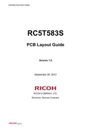
<strong>RN5T566A</strong> PCB LAYOUT GUIDE<br />
<strong>RN5T566A</strong><br />
PCB Layout Guide<br />
Version 1.1<br />
August 31, 2012<br />
RICOH COMPANY, LTD.<br />
Electronic Devices Company<br />
©2012
<strong>RN5T566A</strong> PCB LAYOUT GUIDE<br />
Abstract<br />
This document describes the constraints and points when designing the PCB layout with <strong>RN5T566A</strong>.<br />
This guide provides examples to explain of how it can be done.<br />
The PCB layout example is helpful to achieve optimal <strong>RN5T566A</strong> performance.<br />
Contents<br />
1. Basic Policy and Examples of Board Pattern ............................................................................................. 3<br />
1.1 ..................................................................................................................................... 3<br />
1.2 ........................................................................................................................................ 5<br />
2. Recommended External Parts List ............................................................................................................. 6<br />
3. Example of Parts Layout............................................................................................................................. 8<br />
©2012 Page 2
<strong>RN5T566A</strong> PCB LAYOUT GUIDE<br />
1. Basic Policy and Examples of Board Pattern<br />
1.1 <br />
■ DCDC Simple Schematic<br />
VIN<br />
<strong>RN5T566A</strong><br />
Analog<br />
Power<br />
Supply<br />
Buffer<br />
Power<br />
Supply<br />
Cin_A<br />
R<br />
1<br />
R2<br />
Cf<br />
VFB<br />
VREF<br />
-<br />
+<br />
Control<br />
and<br />
Analog<br />
BUF<br />
LX<br />
Cin_B<br />
L<br />
Cout<br />
Vout<br />
Analog<br />
GND<br />
Buffer<br />
GND<br />
GND<br />
Current Loop<br />
Fig.1-1: DCDC Simple Schematic<br />
<strong>RN5T566A</strong> Pin Names<br />
DCDC1<br />
DCDC2<br />
Analog power supply<br />
VCCA<br />
Buffer power supply VCCP1 VCCP2<br />
VFB VFB1 VFB2<br />
LX LX1 LX2<br />
Table 1-1: <strong>RN5T566A</strong> Pin Names<br />
©2012 Page 3
<strong>RN5T566A</strong> PCB LAYOUT GUIDE<br />
(3)<br />
(4) (8)<br />
Cf<br />
VFB2<br />
(7)<br />
R1<br />
R2<br />
(5)<br />
GND<br />
Cout<br />
VCCP2<br />
Cin<br />
L<br />
(1)<br />
LX2<br />
(6)<br />
(2)<br />
VCCP1<br />
LX1<br />
VFB1<br />
■PCB Layout Procedure for DCDC<br />
Fig.1-2: DCDC Block Evaluation Board Pattern (Top Layer)<br />
(1) Place the parts to minimize the switching current loop (Figure 1-1: blue line, Figure 1-2: red line).<br />
(2) Route the LX line between <strong>RN5T566A</strong> and an inductor as short and wide as possible,<br />
and yet should not add other redundant lines on it<br />
(3) Connect the GND line of “Cout” directly to the internal GND plane with multiple vias, in order to reduce<br />
impedance as small as possible. (Target: 50mΩ or less)<br />
(4) Begin to route the VOUT line from near not “L” but “Cout”.<br />
(5) Place “Cin” as close as possible to <strong>RN5T566A</strong>. (Higher priority level is “Cin” < L < “Cout” in the close<br />
distance order with <strong>RN5T566A</strong>.)<br />
Note: For evaluations being compliant with each DCDC specifications, the PCB layout shown in Fig.1-2<br />
provides the routing for VCCP1 and VCCP2 separately.<br />
But, the routing for them is permitted to unity when designing a PCB layout in actually.<br />
(6) Place inductors for DCDC1 and DCDC2 without becoming too close between them, in order to avoid<br />
the electromagnetic interference.<br />
©2012 Page 4
<strong>RN5T566A</strong> PCB LAYOUT GUIDE<br />
(7) Route the VFB line to be not the parallel routing to other lines, which may cause noise, because of being<br />
easily influenced by noise. Route the VFB line as possible and put some distance from the other lines if<br />
need the parallel routing due to limitations of terminal configuration.<br />
To maintain a stable operation, note against extra parasitic capacitance.<br />
(8) Place R1, R2, and Cf as close as possible in the same layer, and connect GND of R2 to a stable GND.<br />
1.2 <br />
(1)<br />
Vout<br />
Cout<br />
R1<br />
R2<br />
(2)<br />
VFBLDO2<br />
R3<br />
■PCB Layout Procedure for LDO<br />
Fig.1-3: LDO Block Evaluation Board Pattern (Top Layer)<br />
(1) Place “Cout” as close as possible to <strong>RN5T566A</strong> to get better a load regulation.<br />
(2) Route the VFBLDO line output from LDO (LDO2 and LDO4), which can change the output voltage by<br />
external resistors, not to be the parallel routing to the source of noise. In this time, place external<br />
resistors as close as possible to the VFBLDO line, and thereby the extra parasitic capacitance is not<br />
required.<br />
Note: In the evaluation board shown in Fig.1-3, two resistors are placed for the resistance value in the<br />
upper side, in order to control the output easily at the evaluation.<br />
©2012 Page 5
<strong>RN5T566A</strong> PCB LAYOUT GUIDE<br />
2. Recommended External Parts List<br />
<strong>RN5T566A</strong> External Parts<br />
Block Pin Name<br />
Parts Size [mm]<br />
Parts Model value Vender Num<br />
X Size Y Size Z Size [mm2]<br />
PMU - - <strong>RN5T566A</strong> RICOH 1 6.00 6.00 0.90 36<br />
LDO VCCL1 0.1uF GRM155B31E104KA87 Murata 1 1.00 0.50 0.50 0.5<br />
VO1 1.0uF C1005JB1C105K TDK 1 1.00 0.50 0.50 0.5<br />
VO2 2.2uF C1608JB0J225K TDK 1 1.60 0.80 0.80 1.28<br />
VFBLDO2<br />
R1(VO2) - 1 1.00 0.50 0.35 0.5<br />
(Refer to Table 2-2)<br />
R2(VO2) - 1 1.00 0.50 0.35 0.5<br />
VCCL3 VIN GRM155B31E104KA87 Murata 1 1.00 0.50 0.50 0.5<br />
VO3 1.0uF C1005JB1C105K TDK 1 1.00 0.50 0.50 0.5<br />
VO4 1.0uF C1005JB1C105K TDK 1 1.00 0.50 0.50 0.5<br />
VFBLDO4<br />
R1(VO4) - 1 1.00 0.50 0.35 0.5<br />
(Refer to Table 2-2)<br />
R2(VO4) - 1 1.00 0.50 0.35 0.5<br />
VCCL5 VIN GRM155B31E104KA87 Murata 1 1.00 0.50 0.50 0.5<br />
VO5 1.0uF C1005JB1C105K TDK 1 1.00 0.50 0.50 0.5<br />
VCCA 1.0uF C1005JB1C105K TDK 1 1.00 0.50 0.50 0.5<br />
VREFO 1.0uF C1005JB1C105K TDK 1 1.00 0.50 0.50 0.5<br />
INT18 1.0uF C1005JB1C105K TDK 1 1.00 0.50 0.50 0.5<br />
DET R1(DET) - 1 1.00 0.50 0.35 0.5<br />
VD1IN<br />
R2(DET) (Refer to Figure 2-1) - 1 1.00 0.50 0.35 0.5<br />
VD1HYS R3(DET) - 1 1.00 0.50 0.35 0.5<br />
DCDC VCCP1 22uF GRM21BB30J226ME38 Murata 1 2.00 1.25 1.25 2.5<br />
VCCP2<br />
LX1 2.2uH MIPSZ2012D2R2 FDK 1 2.00 1.25 1.00 2.5<br />
47uF C2012X5R0J476M TDK 1 2.00 1.25 1.25 2.5<br />
VFB1<br />
R1(DC1) - 1 1.00 0.50 0.35 0.5<br />
R2(DC1) (Refer to Table 2-3) - 1 1.00 0.50 0.35 0.5<br />
Cf(DC1) - 1 1.00 0.50 0.50 0.5<br />
LX2 2.2uH MIPSZ2012D2R2 FDK 1 2.00 1.25 1.00 2.5<br />
47uF C2012X5R0J476M TDK 1 2.00 1.25 1.25 2.5<br />
VFB2<br />
R1(DC2) - 1 1.00 0.50 0.35 0.5<br />
R2(DC2) (Refer to Table 2-4) - 1 1.00 0.50 0.35 0.5<br />
Cf(DC2) - 1 1.00 0.50 0.50 0.5<br />
Total Num 30 Total Parts size 61.28<br />
Table 2-1: External Parts list<br />
Output Voltage R1 R2<br />
3.30V 230kΩ 100kΩ<br />
3.00V 200kΩ 100kΩ<br />
2.85V 185kΩ 100kΩ<br />
2.80V 180kΩ 100kΩ<br />
1.80V 80kΩ 100kΩ<br />
Table 2-2: LDO2 and LDO4 External Resistor<br />
©2012 Page 6
<strong>RN5T566A</strong> PCB LAYOUT GUIDE<br />
VH = Higher voltage threshold<br />
VL=lower voltage threshold<br />
Vref=reference voltage<br />
Example:<br />
VH=3.4V, VL=3.3V<br />
:R1=240kΩ, R2=100kΩ, R3=4.3kΩ<br />
VL=(R1+R2+R3)/(R2+R3)×Vref<br />
VH=(R1+R2)/R2×Vref<br />
Fig.2-1: Voltage Detection1 Timing<br />
Output Voltage R1 R2 Cf<br />
1.775V 47kΩ 24kΩ 100pF<br />
1.5V 36kΩ 24kΩ 100pF<br />
1.2V 30kΩ 30kΩ 220pF<br />
Table 2-3: Step-down DCDC Converter1 External Components<br />
Output Voltage R1 R2 Cf<br />
1.2V 30kΩ 30kΩ 220pF<br />
1.1V 30kΩ 36kΩ 220pF<br />
1.0V 22kΩ 33kΩ 220pF<br />
Table 2-4: Step-down DCDC Converter2 External Components<br />
©2012 Page 7
<strong>RN5T566A</strong> PCB LAYOUT GUIDE<br />
3. Example of Parts Layout<br />
This layout is one example of parts layout with <strong>RN5T566A</strong><br />
12 mm<br />
2.1 mm<br />
10.4 mm<br />
RN5T<br />
566A<br />
5.7 mm<br />
Total Parts Area 139.49mm 2<br />
3.4 mm<br />
0.8 mm<br />
Fig.3-1: Example of Parts Layout<br />
Note: Connect Exposed Paddle (Tab on the bottom side) to GND.<br />
©2012 Page 8