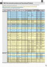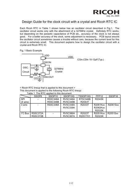
Design Guide for the clock circuit with a crystal and Ricoh RTC IC
Design Guide for the clock circuit with a crystal and Ricoh RTC IC
Design Guide for the clock circuit with a crystal and Ricoh RTC IC

You also want an ePaper? Increase the reach of your titles
YUMPU automatically turns print PDFs into web optimized ePapers that Google loves.
July 24, 2009<br />
<strong>Design</strong> <strong>Guide</strong> <strong>for</strong> <strong>the</strong> <strong>clock</strong> <strong>circuit</strong> <strong>with</strong> a <strong>crystal</strong> <strong>and</strong> <strong>Ricoh</strong> <strong>RTC</strong> <strong>IC</strong><br />
Each <strong>Ricoh</strong> <strong>RTC</strong> in Table 1 shown below has an oscillator <strong>circuit</strong> described in Fig.1. The<br />
oscillator <strong>circuit</strong> works only <strong>with</strong> <strong>the</strong> attachment of a 32768Hz <strong>crystal</strong>. Definitely <strong>RTC</strong> works,<br />
but depending on <strong>the</strong> parasitic capacitance of PCB etc., accuracy of <strong>the</strong> <strong>clock</strong> is not always<br />
good. For a better accuracy of <strong>the</strong> <strong>clock</strong>, some adjustment is necessary. PCB layout around<br />
<strong>the</strong> oscillator <strong>circuit</strong> sometimes causes a trouble <strong>with</strong>out care, because <strong>the</strong> current level <strong>for</strong> this<br />
<strong>circuit</strong> is extremely small. This document explains how to design <strong>the</strong> oscillator <strong>circuit</strong> <strong>with</strong> a<br />
<strong>crystal</strong> <strong>and</strong> <strong>Ricoh</strong> <strong>RTC</strong> <strong>IC</strong>.<br />
Fig. 1 Basic Example<br />
VDD<br />
OSCIN<br />
VDD<br />
CGin,CDin 10-12pF(Typ.)<br />
OSC.<br />
Circuit<br />
CG<br />
32768Hz<br />
Crystal<br />
RD<br />
CD<br />
OSCOUT<br />
< <strong>Ricoh</strong> <strong>RTC</strong> lineup that is applied to this document ><br />
This document is applied to <strong>the</strong> following <strong>Ricoh</strong> <strong>RTC</strong> lineup:<br />
Table 1: The <strong>RTC</strong> applied to this document<br />
SSOP8 SSOP10 SSOP10G TSSOP10G FFP12 SSOP16<br />
SPI<br />
- RS5C348A RV5C348A RT5C348B R2043K<br />
(4 wire)<br />
RS5C348B RV5C348B<br />
3 wire - RS5C338A RV5C338A<br />
RV5C339A<br />
I 2 C Bus<br />
RS5C372A<br />
RS5C372B<br />
- RV5C386A<br />
RV5C387A<br />
R2043T<br />
R2033T<br />
R2023T<br />
R2051T01<br />
R2061Kxx<br />
R2062Kxx<br />
R2033K<br />
R2051Kxx<br />
R2023K<br />
R2061Sxx<br />
R2051Sxx<br />
1/12
1. Characteristics of Oscillator <strong>circuit</strong><br />
1.1. CL value of a <strong>crystal</strong><br />
The load capacitance (CL) of <strong>the</strong> <strong>crystal</strong> is a critical parameter. The CL is not <strong>the</strong> capacitance<br />
of <strong>the</strong> <strong>crystal</strong> itself. CL means an external capacitance in parallel <strong>with</strong> <strong>the</strong> <strong>crystal</strong>.<br />
Each <strong>crystal</strong> manufacturer offers several different CL value <strong>crystal</strong>s <strong>with</strong> <strong>the</strong> same frequency.<br />
When a <strong>crystal</strong> is connected to an oscillator <strong>circuit</strong>, if <strong>the</strong> specified CL value <strong>and</strong> external<br />
capacitance value in parallel <strong>with</strong> <strong>the</strong> <strong>crystal</strong> are <strong>the</strong> same, <strong>the</strong> frequency will be <strong>the</strong> specified<br />
value at normal temperature (25°C).<br />
For example, in <strong>the</strong> Fig2,<br />
When CS+CG×CD/(CG+CD) = CL, <strong>the</strong> <strong>crystal</strong> oscillates at its nominal frequency (32768Hz).<br />
When CS+CG×CD/(CG+CD) > CL, <strong>the</strong> <strong>crystal</strong> oscillates slower than 32768Hz.<br />
Fur<strong>the</strong>r, when CS+CG×CD/(CG+CD) < CL, <strong>the</strong> <strong>crystal</strong> oscillates faster than 32768Hz.<br />
Fig. 2<br />
RF<br />
CG<br />
RD CD<br />
CS<br />
CS: parasitic capacitance<br />
32768Hz<br />
Crystal<br />
We recommend <strong>crystal</strong>s <strong>with</strong> CL ranging from 6 to 8pF <strong>for</strong> our <strong>RTC</strong> <strong>IC</strong>. (CL range is from 6 to<br />
9pF in terms of R2023x, R2033x, R2043x.)<br />
Some <strong>crystal</strong> manufacturers offer a <strong>crystal</strong> <strong>with</strong> CL=12.5pF as a st<strong>and</strong>ard item.<br />
If you choose a <strong>crystal</strong> <strong>with</strong> CL=12.5pF, refer to our “Oscillation frequency calibration <strong>with</strong><br />
CL=12.5pF <strong>crystal</strong> <strong>and</strong> <strong>Ricoh</strong> <strong>RTC</strong> <strong>IC</strong>” (http://www.ricoh.com/LSI/product_rtc/info/125pf-e.pdf).<br />
1.2. Oscillation allowance<br />
To judge <strong>the</strong> oscillator <strong>circuit</strong>, oscillation allowance is a critical parameter. The oscillation<br />
allowance means <strong>the</strong> value of which <strong>the</strong> negative resistance (-r) of <strong>the</strong> oscillator frequency is<br />
divided by maximum equivalent series resistance of <strong>the</strong> <strong>crystal</strong>. Supposed that a resistor is<br />
added to a <strong>crystal</strong> in series as in Fig.3 shown below, <strong>the</strong>n increase <strong>the</strong> resistance value until<br />
oscillator stops. The resistance value just be<strong>for</strong>e stopping <strong>the</strong> oscillation plus equivalent series<br />
resistance is approximately equal to negative resistance value. Considering <strong>the</strong> effect of <strong>the</strong><br />
distribution among products <strong>and</strong> ambient temperature, choose <strong>the</strong> appropriate value <strong>crystal</strong> <strong>and</strong><br />
<strong>the</strong> <strong>IC</strong>. Generally, 5 times is said to be an ideal value. Oscillation allowance is closely related<br />
to <strong>the</strong> value of CG, CD, <strong>and</strong> CS.<br />
Each <strong>Ricoh</strong> <strong>RTC</strong> <strong>IC</strong> has an oscillation booster <strong>circuit</strong> to reduce <strong>the</strong> starting time <strong>for</strong> <strong>RTC</strong>. If <strong>the</strong><br />
oscillation booster detects <strong>the</strong> oscillation halt, <strong>the</strong> booster boosts <strong>the</strong> driver of <strong>the</strong> oscillator in a<br />
certain term. Because of this, if <strong>the</strong> oscillator condition is bad, oscillation stops->oscillator<br />
booster starts->oscillator booster stops -> oscillation stops, <strong>the</strong> cycle will be intermittently<br />
repeated. If this phenomenon happens, <strong>the</strong> <strong>clock</strong> will be delay. There<strong>for</strong>e, to evaluate <strong>the</strong><br />
negative resistance value <strong>and</strong> oscillation allowance, it is necessary to judge <strong>the</strong> oscillation<br />
halting point is when <strong>the</strong> intermittent oscillation starts.<br />
Fig.3<br />
RF<br />
RD<br />
CG<br />
CD<br />
CS<br />
r<br />
CS: Parasitic Capacitance<br />
32768Hz<br />
Crystal<br />
2/12
1.3. Correlation between <strong>the</strong> oscillation stabilize capacitors (CG, CD) <strong>and</strong> o<strong>the</strong>r<br />
characteristics<br />
To compose <strong>the</strong> oscillator <strong>circuit</strong>, check <strong>the</strong> following items:<br />
Oscillator Frequency<br />
Oscillation Maintained Voltage<br />
Consumption Current<br />
Oscillation Allowance<br />
Start-up time <strong>for</strong> oscillation<br />
Graphs which describes <strong>the</strong> frequency, oscillation maintained voltage, consumption current,<br />
oscillation allowance <strong>with</strong> R2051K01 <strong>and</strong> a external CGOUT, are shown below:<br />
Oscillator frequency deviation vs. CGOUT<br />
Ta=25°C, <strong>with</strong> FC135(Seiko Epson)<br />
CGOUT=0pF's deviation=0ppm<br />
0<br />
Consumption current of operating as <strong>clock</strong><br />
vs. CGOUT<br />
Ta=25°C, <strong>with</strong> FC135(Seiko Epson)<br />
0.6<br />
Oscillator Frequency<br />
Deviation ∆f/f0(ppm)<br />
-10<br />
-20<br />
-30<br />
-40<br />
-50<br />
-60<br />
0 5 10 15 20 25<br />
CGOUT(pF)<br />
Operating Consumption<br />
Current (uA)<br />
0.5<br />
0.4<br />
0.3<br />
0.2<br />
0.1<br />
0<br />
0 5 10 15 20 25<br />
CGOUT(pF)<br />
Oscillation maintained voltage vs. CGOUT<br />
Ta=25°C, <strong>with</strong> FC135(Seiko Epson)<br />
Oscillation maintained<br />
voltage(V)<br />
0.8<br />
0.7<br />
0.6<br />
0.5<br />
0.4<br />
0.3<br />
0.2<br />
0.1<br />
0<br />
0 5 10 15 20 25<br />
CGOUT(pF)<br />
Oscillation allowance vs. CGOUT<br />
Ta=25°C, <strong>with</strong> FC135(Seiko Epson)<br />
Oscillation margin<br />
10<br />
9<br />
8<br />
7<br />
6<br />
5<br />
4<br />
3<br />
2<br />
1<br />
0<br />
0 5 10 15 20 25<br />
CGOUT(pF)<br />
General tendency of CG <strong>and</strong> CD vs. characteristics is shown in <strong>the</strong> next table.<br />
Table 2.<br />
Small ValueLarge value<br />
High Oscillator Frequency Low<br />
Low Oscillation maintained voltage High<br />
Small Consumption Current Large<br />
Large Oscillation Allowance Small<br />
Short Oscillation start-up time Long<br />
As described in <strong>the</strong> table shown above, <strong>the</strong> smaller value of CG <strong>and</strong> CD, <strong>the</strong> better <strong>the</strong> most<br />
3/12
characteristics except oscillator frequency are.<br />
As it was mentioned in <strong>the</strong> chapter 1.3 of this document, if you choose a <strong>crystal</strong> <strong>with</strong> small CL,<br />
you can make CG <strong>and</strong> CD small. In o<strong>the</strong>r words, if you choose a <strong>crystal</strong> <strong>with</strong> small CL, most<br />
characteristics shown above will be improved.<br />
1.4. Effect by <strong>the</strong> third capacitance (CS)<br />
In this section, <strong>the</strong> effect by <strong>the</strong> parasitic capacitance of PCB, so-called CS, is described. Next<br />
graphs are <strong>the</strong> typical characteristics of oscillator frequency <strong>and</strong> oscillator frequency deviation<br />
vs. CS.<br />
Sample: RV5C338A<br />
CS value: Instead of actual capacitance, external capacity is used <strong>for</strong> this experiment.<br />
Oscillator frequency deviation vs. CS<br />
Ta=25°C, <strong>with</strong> CFS145(Citizen)<br />
Deviation=0ppm, specified at CGOUT=0pF<br />
Oscillator frequency<br />
deviation ∆f/f0(ppm)<br />
0<br />
-10<br />
-20<br />
-30<br />
-40<br />
-50<br />
-60<br />
-70<br />
-80<br />
-90<br />
-100<br />
0 2 4 6 8 10<br />
CS(pF)<br />
Oscillation start-up time vs. CS<br />
Ta=25°C, <strong>with</strong> CFS145(Citizen)<br />
Oscillator start-up time(s)<br />
20<br />
15<br />
10<br />
5<br />
0<br />
0 2 4 6 8 10 12 14 16<br />
CS(pF)<br />
As <strong>the</strong> graphs shown above, oscillator frequency <strong>and</strong> start-up time varies depending on CS<br />
value.<br />
There<strong>for</strong>e, make <strong>the</strong> wiring as short as possible to reduce <strong>the</strong> parasitic capacity of PCB,<br />
especially, board layout which <strong>the</strong> capacity is generated between OSCIN <strong>and</strong> OSCOUT, should<br />
be avoided.<br />
1.5. Measurement of Oscillator Frequency<br />
To check <strong>the</strong> frequency, <strong>the</strong>re are some tips to measure <strong>the</strong> correct frequency. If you use<br />
probes <strong>for</strong> OSCIN <strong>and</strong> OSCOUT directly, frequency will vary because of <strong>the</strong> capacitance of<br />
probes. Generally, probes have approximately 15pF capacitance. As <strong>the</strong> graph shown in<br />
“Oscillator frequency deviation vs. CGOUT” in page 3, when <strong>the</strong> capacitance <strong>for</strong> CGOUT is<br />
15pF, frequency varies approximately 40ppm. To avoid this, our option is useful.<br />
Most of <strong>Ricoh</strong> <strong>RTC</strong> has 32k <strong>clock</strong> output pin. From this pin, <strong>the</strong> <strong>IC</strong> outputs <strong>the</strong> <strong>clock</strong> <strong>with</strong> same<br />
frequency as <strong>the</strong> oscillator <strong>circuit</strong>, <strong>and</strong> if some capacities are added, <strong>the</strong> frequency is<br />
maintained.<br />
When you check <strong>the</strong> frequency, we recommend using this 32k output pin.<br />
In terms of R2061K01, <strong>the</strong>re is no 32k output pin. However, <strong>the</strong> interrupt pin can output 1Hz<br />
<strong>clock</strong> <strong>with</strong> a specific setting. If <strong>clock</strong> adjustment register is not set, <strong>the</strong> frequency of <strong>the</strong> <strong>circuit</strong><br />
is 32768 times of <strong>the</strong> measured 1Hz <strong>clock</strong>.<br />
4/12
1.6. Oscillator Frequency Dispersion data caused by <strong>IC</strong>s<br />
Supposed that <strong>the</strong> <strong>crystal</strong> has no dispersion, if <strong>the</strong> <strong>IC</strong> is replaced to o<strong>the</strong>r <strong>IC</strong>, capacity of <strong>the</strong> <strong>IC</strong><br />
itself is different, so frequency may change. For your reference, dispersion of <strong>the</strong> oscillator<br />
frequency deviation by <strong>IC</strong> graph is shown below:<br />
RV5C338A oscillator frequency dispersion<br />
Samples: 98lots, 5pieces from each lot are measured.<br />
Crystal: MS2V-TS, CL=7pF(Micro Crystal)<br />
Ta=23°C, VDD=3V, <strong>with</strong> a socket. 0ppm considered as average, <strong>and</strong> redistributed.<br />
140<br />
120<br />
100<br />
number<br />
80<br />
60<br />
40<br />
20<br />
0<br />
-4 -3.5 -3 -2.5 -2 -1.5 -1 -0.5 0 0.5 1 1.5 2 2.5 3 3.5 4<br />
Oscillator Frequency Deviatiion(ppm)<br />
In <strong>the</strong> graph above, <strong>for</strong> example <strong>the</strong> position of horizontal "0ppm", vertical number means <strong>the</strong><br />
number of samples ranging from -0.5 to 0.0ppm frequency deviation. St<strong>and</strong>ard deviation of<br />
<strong>the</strong> graph is 0.99ppm.<br />
1.7. Oscillator frequency <strong>and</strong> monthly error<br />
Generally, <strong>the</strong> unit shown <strong>the</strong> oscillator frequency deviation is ppm. On <strong>the</strong> o<strong>the</strong>r h<strong>and</strong>, <strong>the</strong><br />
error of <strong>the</strong> <strong>clock</strong> is described as monthly error.<br />
For example, ±10ppm error is equal to ±10*10 -6 *60*60*24*30=±25.9s/month. ±23ppm error is<br />
almost equal to one minute per month error.<br />
5/12
2. Notes on PCB layout<br />
This section describes <strong>the</strong> technical notes on PCB layout.<br />
(1) Pins of <strong>the</strong> <strong>crystal</strong> <strong>and</strong> OSCIN/OSCOUT pins of real time <strong>clock</strong> should be as close as<br />
possible to reduce <strong>the</strong> parasitic capacitance.<br />
(2) Avoid <strong>the</strong> long parallel pattern or cross pattern of OSCIN <strong>and</strong> OSCOUT.<br />
(3) OSCIN/OSCOUT lines <strong>and</strong> o<strong>the</strong>r lines should be as far as possible <strong>and</strong> <strong>the</strong>y should not be<br />
crossed.<br />
Oscillator frequency <strong>circuit</strong>'s current capacity is limited to reduce <strong>the</strong> consumption current.<br />
There<strong>for</strong>e, <strong>the</strong>y are sensitive against <strong>the</strong> noise.<br />
(4) If possible, we recommend a guard ring <strong>with</strong> GND line around oscillator <strong>circuit</strong>, <strong>and</strong> <strong>the</strong> layer<br />
right under this pattern, put <strong>the</strong> GND plane to make a light shield against noise. To set <strong>the</strong> real<br />
time <strong>clock</strong> <strong>IC</strong> <strong>and</strong> <strong>crystal</strong> far from o<strong>the</strong>r lines' noise, putting <strong>the</strong>m at <strong>the</strong> side of <strong>the</strong> PCB is<br />
ano<strong>the</strong>r good idea.<br />
Fig.4<br />
Guardring<br />
OSCIN<br />
OSCOUT<br />
Crystal<br />
VSS<br />
GND plane :Just under this part<br />
In terms of R2051Sxx <strong>and</strong> R2061Sxx, to make <strong>the</strong> layout as above easy, OSCIN/OSCOUT pins<br />
are between NC pins, which can be connected to <strong>the</strong> GND.<br />
Fig.5<br />
R2051Sxx(SSOP16)<br />
NC<br />
1<br />
16<br />
VCC<br />
VSB<br />
2<br />
15<br />
VDD<br />
CLKOUT<br />
3<br />
14<br />
NC<br />
SCL<br />
4<br />
13<br />
OSCIN<br />
SDA<br />
NC<br />
5<br />
6<br />
12<br />
11<br />
OSCOUT<br />
NC<br />
/VDCC<br />
7<br />
10<br />
/INTR<br />
VSS<br />
8<br />
9<br />
CIN<br />
TOP VIEW<br />
6/12
3. Adjustment of gain <strong>and</strong> loss of <strong>the</strong> <strong>clock</strong><br />
3.1. Conventional adjustment method of oscillator frequency<br />
CG <strong>and</strong> CD are built-in <strong>the</strong> most of <strong>Ricoh</strong> real time <strong>clock</strong> <strong>IC</strong>s. However, depending on <strong>the</strong><br />
capacitance of <strong>the</strong> PCB, <strong>and</strong> characteristics of <strong>the</strong> <strong>crystal</strong>, adjustment might be necessary.<br />
As a conventional method, adjustment is possible as in <strong>the</strong> Fig. 6.<br />
If <strong>the</strong> larger CGOUT/CDOUT is set, frequency will be low. On <strong>the</strong> contrary, if <strong>the</strong> smaller<br />
capacitors are set, frequency will be high.<br />
Note that large capacitance may cause increase of <strong>the</strong> time keeping current <strong>and</strong> oscillation<br />
maintained voltage, <strong>and</strong> decrease <strong>the</strong> oscillation allowance, <strong>and</strong> change <strong>the</strong> oscillation start-up<br />
time.<br />
Fig.6<br />
Oscillation<br />
Circuit<br />
CG<br />
RD<br />
CD<br />
OSCIN<br />
32kHz<br />
OSCOUT<br />
CGOUT<br />
CDOUT<br />
3.2. Adjustment <strong>with</strong> Software calibration<br />
Without additional CGOUT/CDOUT, adjustment of gain <strong>and</strong> loss of <strong>the</strong> <strong>clock</strong> is possible.<br />
The oscillator calibration <strong>circuit</strong> is configured to change time counts of 1 second on <strong>the</strong> basis of<br />
<strong>the</strong> settings of <strong>the</strong> oscillation calibration register once in 20seconds or once in one minute.<br />
The advantage of this method is that <strong>the</strong> time keeping current, oscillation maintained voltage,<br />
oscillation allowance, oscillation start-up time can be kept its original characteristics because it<br />
is not necessary to change <strong>the</strong> oscillator <strong>circuit</strong> itself.<br />
If <strong>the</strong> <strong>clock</strong> gains, write <strong>the</strong> calculated value <strong>for</strong> adjustment to <strong>the</strong> <strong>clock</strong> adjustment register of<br />
<strong>the</strong> <strong>clock</strong>.<br />
Adjustment value =(Measured frequency-Target frequency)×10+1<br />
Excel software file <strong>for</strong> executing this calculation is on our Web site.<br />
http://www.ricoh.com/LSI/product_rtc/<br />
If following 3 conditions are completed, actual <strong>clock</strong> adjustment value could be different from<br />
target adjustment value that set by oscillator adjustment function.<br />
1. Using oscillator adjustment function<br />
2. Access to <strong>RTC</strong> at r<strong>and</strong>om, or synchronized <strong>with</strong> external <strong>clock</strong> that has no relation to <strong>RTC</strong>, or<br />
synchronized <strong>with</strong> periodic interrupt in pulse mode.<br />
3. Access to <strong>RTC</strong> more than 2 times per each second on average.<br />
For more details, please contact to <strong>Ricoh</strong>.<br />
7/12
3.3. Evaluation <strong>and</strong> Confirmation method <strong>for</strong> software calibration of <strong>the</strong> <strong>clock</strong><br />
The <strong>clock</strong> adjustment <strong>circuit</strong> is configured to change time counts of 1 second on <strong>the</strong> basis of <strong>the</strong><br />
settings of <strong>the</strong> <strong>clock</strong> adjustment register once in 20seconds. The <strong>clock</strong> adjustment pulse output<br />
from <strong>the</strong> 32KOUT pin. There<strong>for</strong>e, after writing <strong>the</strong> <strong>clock</strong> adjustment register, we cannot measure<br />
<strong>the</strong> <strong>clock</strong> error <strong>with</strong> probing 32KOUT <strong>clock</strong> pulses. The way to measure <strong>the</strong> <strong>clock</strong> error as<br />
follows:<br />
(1) Output a 1Hz <strong>clock</strong> pulse of Pulse Mode <strong>with</strong> interrupt pin<br />
Each <strong>RTC</strong> has different 1Hz output pin <strong>and</strong> <strong>the</strong> way to set <strong>the</strong> register.<br />
Refer to <strong>the</strong> Table 3.<br />
Table 3: 1Hz output pin <strong>and</strong> <strong>the</strong> way to set <strong>the</strong> register <strong>for</strong> output 1Hz <strong>clock</strong><br />
Setting<br />
Output Pin<br />
RS5C372A<br />
Address Eh ← (00000011) /INTRA(5pin)<br />
RS5C372B<br />
/INTR(5pin)<br />
RS/RV5C338A<br />
/INTR(6pin)<br />
RV5C339A<br />
Address Eh ← (00XX0011) /INTRA(6pin)<br />
RS/RV/RT5C348A/B, R2043T<br />
/INTR(6pin)<br />
RV5C386A/387A,R2023T<br />
/INTRA(6pin)<br />
R2043K,R2033K<br />
/INTR(10pin)<br />
R2023K<br />
/INTRA(10pin)<br />
R2051Kxx,R2061Kxx, R2062Kxx<br />
/INTR(9pin)<br />
R2051Sxx,R2061Sxx<br />
/INTR(10pin)<br />
(2) After setting <strong>the</strong> <strong>clock</strong> calibration register, 1Hz <strong>clock</strong> period changes every 20seconds as in<br />
Fig. 7.<br />
Fig.7<br />
1Hz <strong>clock</strong> pulse<br />
T0 T0 T0 T1<br />
19 times<br />
1 time<br />
Measure <strong>the</strong> interval of T0 <strong>and</strong> T1 <strong>with</strong> frequency counter. A frequency counter <strong>with</strong> 7 or more<br />
digits is recommended <strong>for</strong> <strong>the</strong> measurement.<br />
(3) Calculate <strong>the</strong> typical period from T0 <strong>and</strong> T1<br />
T=(19×T0+1×T1)/20<br />
Calculate <strong>the</strong> time error from T.<br />
This method can be used under development stage, <strong>for</strong> mass production, this method is<br />
time-consuming. The <strong>circuit</strong> <strong>for</strong> oscillator calibration of <strong>the</strong> <strong>clock</strong> is digital base, <strong>the</strong>re<strong>for</strong>e, <strong>with</strong><br />
32k <strong>clock</strong> frequency <strong>and</strong> calculated value, exact gain <strong>and</strong> loss of <strong>the</strong> <strong>clock</strong> can be <strong>for</strong>eseen.<br />
3.4. Notes on using <strong>the</strong> oscillator calibration <strong>circuit</strong><br />
When using <strong>the</strong> oscillator calibration <strong>circuit</strong>,<br />
(1) <strong>Ricoh</strong>’s <strong>RTC</strong> does not have non-volatile memory. There<strong>for</strong>e, <strong>the</strong> system must store <strong>the</strong><br />
oscillator adjustment value to non-volatile memory external of <strong>the</strong> <strong>RTC</strong>. The system must write<br />
<strong>the</strong> oscillation adjustment value to <strong>RTC</strong>, when setting <strong>the</strong> <strong>clock</strong> <strong>and</strong> calendar data.<br />
(2) Oscillation Adjustment Circuit does not affect <strong>the</strong> frequency of 32768Hz-<strong>clock</strong> pulse output<br />
from <strong>the</strong> 32KOUT pin. If <strong>the</strong> frequency of <strong>clock</strong> pulse from 32KOUT pin should be accurate, use<br />
<strong>the</strong> conventional adjustment method, or change <strong>the</strong> CL value of <strong>the</strong> <strong>crystal</strong>.<br />
8/12
3.5. Appropriate target frequency<br />
The temperature characteristic of discreet 32768Hz <strong>crystal</strong> is described as following <strong>for</strong>mula:<br />
∆f/f0=α(T-θT) 2 +(f0-fs)/f0<br />
Peak temperature: θT=25±5°C<br />
Temperature coefficient: α=(-0.035±0.005)*10 -6 /°C 2<br />
Nominal Frequency: fs=32768Hz<br />
Frequency at peak temperature: f0<br />
For adjustment of gain <strong>and</strong> loss of <strong>the</strong> <strong>clock</strong>, <strong>with</strong> <strong>the</strong> conventional method, f0 is adjusted <strong>with</strong><br />
external capacitors. In <strong>the</strong> case of adjustment <strong>with</strong> <strong>the</strong> oscillator calibration <strong>circuit</strong>, f0 is<br />
substantially adjusted in different way.<br />
Considering <strong>the</strong> whole oscillator <strong>circuit</strong>, <strong>the</strong> real time <strong>clock</strong> <strong>IC</strong> has also temperature coefficient,<br />
but it is much smaller than equivalent of <strong>crystal</strong>. There<strong>for</strong>e, <strong>the</strong> temperature characteristics of<br />
<strong>the</strong> <strong>IC</strong> can be ignored.<br />
Typical temperature characteristic of <strong>the</strong> <strong>crystal</strong> is as follows:<br />
9/12
Frequency of <strong>the</strong> <strong>crystal</strong> vs. temperature (Typ.)<br />
Oscillator Frequency Deviation<br />
df/f0(ppm)<br />
20<br />
0<br />
-20<br />
-40<br />
-60<br />
-80<br />
-100<br />
-120<br />
-140<br />
-160<br />
-50 -25 0 25 50 75 100<br />
Temperature Topt(°C)<br />
As <strong>the</strong> graph shown above, frequency temperature characteristic of <strong>the</strong> <strong>crystal</strong> is <strong>the</strong> parabola<br />
of which <strong>the</strong> peak is at 25°C.<br />
Supposed that target frequency, f0=32768Hz, <strong>the</strong>n, if <strong>the</strong> temperature rises, or falls, <strong>the</strong> <strong>clock</strong><br />
will lose.<br />
There<strong>for</strong>e, normally, to gain <strong>for</strong> <strong>the</strong> <strong>clock</strong> at 25°C, adjustment is done. The level of gain<br />
depends on <strong>the</strong> place <strong>and</strong> <strong>the</strong> environment where <strong>the</strong> application will be used.<br />
In <strong>the</strong> next table, appropriate f0 value list <strong>for</strong> <strong>the</strong> area. Data source is <strong>the</strong> Meteorological<br />
Agency.<br />
Appropriate f0 list from annual average temperature data by area<br />
f0 Oscillator Frequency<br />
Deviation (f0-fs)/f0<br />
Sapporo 32768.42Hz 12.7ppm<br />
Tokyo 32768.16Hz 4.7ppm<br />
Nagano 32768.28Hz 8.6ppm<br />
Naha 32768.03Hz 0.9ppm<br />
Calculation is done, based on <strong>the</strong> hourly temperature data by <strong>the</strong> Meteorological Agency<br />
in 2000.<br />
Temperature is measured in <strong>the</strong> ventilated case <strong>for</strong> meteorological instruments in 1.5m altitude<br />
If <strong>the</strong> application is used at <strong>the</strong> room temperature, <strong>the</strong> temperature variation is more moderate<br />
than actual outside temperature, <strong>the</strong>re<strong>for</strong>e, f0 is not so large.<br />
Generally, f0's ranging from 32768.1Hz to 32768.2Hz, or frequency deviation is adjusted from 3<br />
to 6ppm.<br />
10/12
4. Trouble Shooting<br />
4.1. Clock gains<br />
(1) Case: The <strong>clock</strong> gains 5 to 9 seconds a day. (60 to 100ppm gain)<br />
Estimated cause) <strong>Ricoh</strong> <strong>RTC</strong> recommends a <strong>crystal</strong> <strong>with</strong> CL=6 to 8pF. On <strong>the</strong> o<strong>the</strong>r h<strong>and</strong>,<br />
some <strong>crystal</strong> manufacturers designate <strong>crystal</strong>s <strong>with</strong> CL=12.5pF are st<strong>and</strong>ard items. If such<br />
<strong>crystal</strong>s are used <strong>with</strong> <strong>Ricoh</strong> <strong>RTC</strong>, built-in capacitance of <strong>the</strong> <strong>IC</strong> <strong>and</strong> CL value matching will be<br />
bad, <strong>the</strong>re<strong>for</strong>e <strong>the</strong> <strong>clock</strong> gains 60 to 100ppm.<br />
Countermeasure) Change <strong>the</strong> <strong>crystal</strong> to <strong>the</strong> appropriate one <strong>with</strong> CL=6 to 8 pF or adjust it <strong>with</strong><br />
referring to chapter 3.2 of this document. If you choose <strong>the</strong> <strong>crystal</strong> <strong>with</strong> CL=12.5pF (or<br />
CL=9pF except R2023x, R2033x, R2043x), ano<strong>the</strong>r reference is “Oscillation frequency<br />
calibration <strong>with</strong> CL=12.5pF <strong>crystal</strong> <strong>and</strong> <strong>Ricoh</strong> <strong>RTC</strong> <strong>IC</strong>”<br />
(http://www.ricoh.com/LSI/product_rtc/info/125pf-e.pdf).<br />
(2) Case: The <strong>clock</strong> gains about 35 minutes a day. (<strong>with</strong> RS5C372A/B)<br />
Estimated cause) RS5C372A/B can use both <strong>crystal</strong>s of 32768Hz <strong>and</strong> 32000Hz. If <strong>the</strong> <strong>RTC</strong> is<br />
used <strong>with</strong> 32768Hz <strong>crystal</strong> at 32000Hz mode, <strong>the</strong> <strong>clock</strong> gains 35 minutes per day.<br />
Countermeasure) Write "0" to D7, /XSL bit of <strong>the</strong> address 7h <strong>and</strong> use <strong>the</strong> 32768Hz mode.<br />
When <strong>the</strong> time is set, write "0" to this bit is recommended procedure.<br />
4.2. Clock loses/ stops<br />
(1) Case: The <strong>clock</strong> loses 34 minutes per hour. (RS/V5C338A, RV5C339A, RS/V5C348A/B)<br />
Estimated cause) The RS/V5C338A, RV5C339A, <strong>and</strong> <strong>the</strong> RS/V5C348A/B have <strong>the</strong> unique<br />
mode. If "1" is written to (0), D7 of <strong>the</strong> address 7h, <strong>clock</strong> loses 56% of <strong>the</strong> normal mode.<br />
Countermeasure) Write "0" to (0), D7 of <strong>the</strong> address 7h, use <strong>with</strong> <strong>the</strong> normal mode. When <strong>the</strong><br />
time is set, write "0" to this bit is recommended procedure.<br />
(2) Case: The oscillation is intermittent <strong>and</strong> <strong>the</strong> <strong>clock</strong> loses.<br />
Estimated cause) Oscillation booster <strong>circuit</strong> is built in <strong>Ricoh</strong> <strong>RTC</strong> <strong>IC</strong>s to shorten <strong>the</strong> oscillation<br />
start-up time. The oscillation booster drives <strong>the</strong> oscillator inverter <strong>for</strong> a certain time if <strong>the</strong> <strong>RTC</strong><br />
detects <strong>the</strong> halt of <strong>the</strong> oscillator. If <strong>the</strong> oscillation conditions are bad, operation cycle will be<br />
that <strong>the</strong> oscillation stops, <strong>the</strong> booster starts, <strong>the</strong> oscillation booster stops, <strong>the</strong>n oscillation stops.<br />
The operation becomes intermittent, <strong>and</strong> if <strong>the</strong> intermittent oscillation occurs, <strong>the</strong> <strong>clock</strong> will lose.<br />
Countermeasure) Use smaller capacitance as CGOUT <strong>and</strong> CDOUT than present value. If <strong>the</strong><br />
<strong>clock</strong> gains, refer to <strong>the</strong> chapter 4.1 of this document <strong>and</strong> adjust it.<br />
(3) Case: Oscillation stops because of <strong>the</strong> temperature change. ( The <strong>clock</strong> stops.)<br />
Estimated cause) Because of condensation, leakage between oscillator pins <strong>and</strong> o<strong>the</strong>r pin is<br />
generated <strong>and</strong> oscillation stops.<br />
Countermeasure) Coating pins of <strong>the</strong> oscillator <strong>circuit</strong> <strong>and</strong> oscillator pins of <strong>the</strong> <strong>IC</strong> <strong>with</strong> <strong>the</strong><br />
materials which have high electric conductivity is necessary.<br />
As <strong>for</strong> <strong>the</strong> oscillator <strong>circuit</strong>s of R2051/61/62, R2043, R2023, R2033 or after <strong>the</strong>se part numbers,<br />
<strong>the</strong> <strong>circuit</strong> against <strong>the</strong> condensation exists, <strong>the</strong>re<strong>for</strong>e leakage between power supply, Vss pin,<br />
OSCIN, <strong>and</strong> OSCOUT is much less than be<strong>for</strong>e.<br />
11/12
12/12