wlcsp-11-p2 - Ricoh
wlcsp-11-p2 - Ricoh
wlcsp-11-p2 - Ricoh

You also want an ePaper? Increase the reach of your titles
YUMPU automatically turns print PDFs into web optimized ePapers that Google loves.
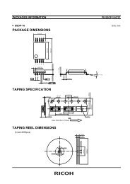
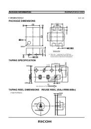
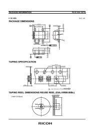
PACKAGE INFORMATION<br />
PE-WLCSP-<strong>11</strong>-P2-07<strong>11</strong>06<br />
RECOMMENDED LAND PATTERN<br />
Solder Mask<br />
(resist)<br />
Copper Pad<br />
Substrate<br />
NSMD<br />
SMD<br />
(Unit : mm)<br />
NSMD and SMD Pad Definition<br />
Pad definition Copper Pad Solder Mask Opening<br />
NSMD (Non-Solder Mask defined) 0.20mm Min. 0.30mm<br />
SMD (Solder Mask defined) Min. 0.30mm 0.20mm<br />
* Pad layout and size can be modified by customers material, equipment, method.<br />
* Please adjust pad layout according to your conditions.<br />
* Recommended Stencil Aperture Size....ø0.3mm<br />
* Since lead free WL-CSP components are not compatible with the tin/lead solder process, you shall not mount lead free WL-CSP<br />
components using the tin/lead solder paste.