Create successful ePaper yourself
Turn your PDF publications into a flip-book with our unique Google optimized e-Paper software.
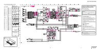
5. AM DEMODULATOR TDA9830<br />
The TDA9830 is designed for AM-sound demodulation used in L and L’ standard.<br />
Sound IF Input:<br />
The sound IF amplifier consists of three AC-coupled differential amplifier stages each with approximately 20dB gain.<br />
At the output of each stage is a multiplier for gain controlling. The overall control range is approximately -6 to +60dB and the<br />
frequency response (-3dB) of the IF amplifier is approximately 6 to 70MHz. The steepness of gain control is approximately 10mV/dB.<br />
IF AGC:<br />
The automatic gain control voltage to maintain the AM demodulator output signal at a constant level is generated by a mean<br />
level detector.The AGC-detector charges and discharges the capacitor at pin 3 controlled by the output signal of the<br />
AM-demodulator compared to an internal reference voltage.The maximum charge/discharge current is approximately 5 mA.<br />
AM-demodulator<br />
The IF amplifier output signal is fed to a limiting amplifier (two stages) and to a multiplier circuit.<br />
However the limiter output signal (which is not any more AM modulated) is also fed to the multiplier, which provides AM<br />
demodulation (in phase demodulation). After lowpass filtering (fg @ 400kHz) for carrier rejection and buffering,<br />
the demodulator output signal is present at pin 6.<br />
Audio Switch<br />
This circuit is an operational amplifier with three input stages and internal feedback network determining gain (0dB) and<br />
frequency response (fg @ 700kHz). Two of the input stages are connected to pin 7 and pin 9, the third input stage to an<br />
internal reference voltage. Controlled by the switching pins 10 and 12, one of the three input stages can be activated and a<br />
choice made between two different AF signals or mute state. The selected signal is present at pin 8. The decoupling capacitors<br />
at the input pins are needed, because the internally generated bias voltage for the input stages must not be influenced<br />
by the application in order to avoid DC-plop in case of switching.<br />
Reference Circuit:<br />
This circuit is a band gap stabiliser in combination with a voltage regulation amplifier, which provides an internal reference voltage<br />
of about 3.6V nearly independent from supply voltage and temperature. This reference voltage is filtered by the capacitor at<br />
pin 4 in order to reduce noise. It is used as a reference to generate all important voltages and currents of the circuit.<br />
For application in 12V power supply concepts, there is an internal voltage divider in combination with a Darlington transistor in<br />
order to reduce the supply voltage for all IC function blocks to approximately 6V.<br />
6. MULTISTANDARD SOUND PROCESSOR:<br />
The MSP 34x0D is designed to perform demodulation of FM or AM-Mono TV sound. Alternatively, two-carrier FM systems<br />
according to the German or Korean terrestrial specs or the satellite specs can be processed with the MSP 34x0D.<br />
Digital demodulation and decoding of NICAM-coded TV stereo sound, is done only by the MSP 3410. The MSP 34x0D offers<br />
a powerful feature to calculate the carrier field strength which can be used for automatic standard detection (terrestrial) and<br />
search algorithms (satellite).<br />
7. SOUND OUTPUT STAGE TDA2614/TDA2615/TDA2616Q<br />
TDA2614 is used as the AF output amplifier for mono applications. It is supplied by ±12VDC coming from a separate winding in the<br />
SMPS transformer. An output power of 2*6W (THD=0.5%) can be delivered into an 8ohm load.<br />
TDA2615 is used as the AF output amplifier for stereo applications. It is supplied by<br />
±12VDC coming from a separate winding in the SMPS transformer. An output power of 2*6W (THD=0.5%)<br />
can be delivered into an 8ohm load.<br />
TDA2616Q is used as the AF output amplifier for stereo and dolby prologic applications. It is supplied by ±16VDC coming from<br />
a separate winding in the SMPS transformer. An output power of 2*12W (THD=0.5%) can be delivered into an 8ohm load.<br />
8. VERTICAL OUTPUT STAGE WITH TDA8351/8356<br />
The TDA8351/8356 vertical deflection circuit can be used in 90° and 110° deflection systems with field frequencies from<br />
50 up to 120Hz. With its bridge configuration the deflection output can be DC coupled with few external components.<br />
Only a single supply voltage for the scan and a second supply for the flyback are needed. The TDA8356 is intended for 90°<br />
systems and the TDA8351 is intended for 110° systems.<br />
The drive voltage is amplified by an amplifier and fed to two amplifiers, one is inverting and the other is a non inverting amplifier.<br />
The outputs (pins 7 and 4) are connected to the series connection of the vertical deflection coil and feedback resistor Rsense<br />
(R702//R703). The voltage across Rsense is fed via pin 9 to correction amplifier, to obtain a deflection current which is proportional<br />
to the drive voltage. The supply voltage for the TDA8351/8356 is 15VDC at pin 3. The supply voltage generator has a separate<br />
supply voltage of 45VDC at pin 6.<br />
9. VIDEO OUTPUT AMPLIFIER TDA6108M<br />
The TDA6108M consists of three monolithic video output amplifiers. The amplifier can be seen as an operational amplifier<br />
with negative feedback.<br />
The advantage of negative feedback is that the amplifier characteristics do not play an important role up to certain frequencies.<br />
The internal flash diodes protect the amplifiers against flash over in the picture tube.<br />
The only protections required at the cathode outputs are a flash resistor and a sparkgap.<br />
The TDA6108M has an internal thermal protection circuit which gives a decrease of the slew rate at high temperatures.<br />
Furthermore, the device needs only one power supply voltage (Vdd).<br />
In contrast to previous types of DMOS video amplifiers, all the external resistors (Rf, Ri and Ra) are integrated, so the gain is fixed<br />
and saves 9 resistors.<br />
Furthermore, the reference voltage is integrated, it saves a resistor divider and a decoupling capacitor. So, the replacement<br />
value of the TDA6108MQ is very high.<br />
The TDA6108M is provided with a black current data pin. Since TDA884X is used as drive device, no adjustments are required<br />
for gain and black setting, as the TDA884X has I²C white point adjustment and black current set-up.<br />
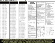
5