CONTENTS - Reptips
CONTENTS - Reptips CONTENTS - Reptips
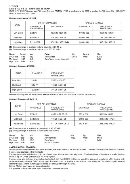
3. TUNER Either a PLL or a VST tuner is used as a tuner. UV1316 (VHF/UHF) is used as a PLL tuner. For only PALM/N, NTSC M applications UV 1336 is used as the PLL tuner. UV 1315 (VHF/ UHF) is used as a VST Tuner. Channel coverage of UV1316: BAND OFF-AIR CHANNELS CABLE CHANNELS CHANNELS FREQUENCY CHANNELS FREQUENCY RANGE (MHz) RANGE (MHz) Low Band E2 to C 48.25 to 82.25 (1) S01 to S08 69.25 to 154.25 Mid Band E5 to E12 175.25 to 224.25 S09 to S38 161.25 to 439.25 High Band E21 to E69 471.25 to 855.25 (2) S39 to S41 447.25 to 463.25 (1). Enough margin is available to tune down to 45.25 MHz. (2). Enough margin is available to tune up to 863.25 MHz. Noise Typical Max. Gain Min. Typical Max. Low band : 5dB 9dB All channels : 38dB 44dB 52dB Mid band : 5dB 9dB Gain Taper (of-air channels) : - - 8dB High band : 6dB 9dB Channel Coverage UV1336: BAND CHANNELS FREQUENCY RANGE (MHz) Low Band 2 to D 55.25 to 139.25 Mid Band E to PP 145.25 to 391.25 High Band QQ to 69 397.25 to 801.25 Noise is typically 6dB for all channels. Gain is minimum 38dB and maximum 50dB for all channels. Channel Coverage of UV1315: BAND OFF-AIR CHANNELS CABLE CHANNELS CHANNELS FREQUENCY CHANNELS FREQUENCY RANGE (MHz) RANGE (MHz) Low Band E2 to C 48.25 to 82.25 (1) S01 to S10 69.25 to 168.25 Mid Band E5 to E12 175.25 to 224.25 S11 to S39 231.25 to 447.25 High Band E21 to E69 471.25 to 855.25 (2) S40 to S41 455.25 to 463.25 (1). Enough margin is available to tune down to 45.25 MHz. (2). Enough margin is available to tune up to 863.25 MHz. Noise Typ. Max. Gain Min. Typ. Max. Low band : 6dB 9dB All Channels 38dB 44dB 50dB Mid band : 6dB 10dB Gain Taper - - 8dB High band : 6dB 11dB (off-air channels) 4.VIDEO SWITCH TEA6415C In case of three or more external sources are used, the video switch IC TEA6415C is used. The main function of this device is to switch 8 video input sources on the 6 outputs. Each output can be switched on only one of each input. On each input an alignment of the lowest level of the signal is made (bottom of sync. top for CVBS or black level for RGB signals). Each nominal gain between any input and output is 6.5dB.For D2MAC or Chroma signal the alignment is switched off by forcing, with an external resistor bridge, 5VDC on the input. Each input can be used as a normal input or as a MAC or Chroma input (with external resistor bridge). All the switching possibilities are changed through the BUS. Driving 75ohm load needs an external resistor. It is possible to have the same input connected to several outputs. 4
5. AM DEMODULATOR TDA9830 The TDA9830 is designed for AM-sound demodulation used in L and L’ standard. Sound IF Input: The sound IF amplifier consists of three AC-coupled differential amplifier stages each with approximately 20dB gain. At the output of each stage is a multiplier for gain controlling. The overall control range is approximately -6 to +60dB and the frequency response (-3dB) of the IF amplifier is approximately 6 to 70MHz. The steepness of gain control is approximately 10mV/dB. IF AGC: The automatic gain control voltage to maintain the AM demodulator output signal at a constant level is generated by a mean level detector.The AGC-detector charges and discharges the capacitor at pin 3 controlled by the output signal of the AM-demodulator compared to an internal reference voltage.The maximum charge/discharge current is approximately 5 mA. AM-demodulator The IF amplifier output signal is fed to a limiting amplifier (two stages) and to a multiplier circuit. However the limiter output signal (which is not any more AM modulated) is also fed to the multiplier, which provides AM demodulation (in phase demodulation). After lowpass filtering (fg @ 400kHz) for carrier rejection and buffering, the demodulator output signal is present at pin 6. Audio Switch This circuit is an operational amplifier with three input stages and internal feedback network determining gain (0dB) and frequency response (fg @ 700kHz). Two of the input stages are connected to pin 7 and pin 9, the third input stage to an internal reference voltage. Controlled by the switching pins 10 and 12, one of the three input stages can be activated and a choice made between two different AF signals or mute state. The selected signal is present at pin 8. The decoupling capacitors at the input pins are needed, because the internally generated bias voltage for the input stages must not be influenced by the application in order to avoid DC-plop in case of switching. Reference Circuit: This circuit is a band gap stabiliser in combination with a voltage regulation amplifier, which provides an internal reference voltage of about 3.6V nearly independent from supply voltage and temperature. This reference voltage is filtered by the capacitor at pin 4 in order to reduce noise. It is used as a reference to generate all important voltages and currents of the circuit. For application in 12V power supply concepts, there is an internal voltage divider in combination with a Darlington transistor in order to reduce the supply voltage for all IC function blocks to approximately 6V. 6. MULTISTANDARD SOUND PROCESSOR: The MSP 34x0D is designed to perform demodulation of FM or AM-Mono TV sound. Alternatively, two-carrier FM systems according to the German or Korean terrestrial specs or the satellite specs can be processed with the MSP 34x0D. Digital demodulation and decoding of NICAM-coded TV stereo sound, is done only by the MSP 3410. The MSP 34x0D offers a powerful feature to calculate the carrier field strength which can be used for automatic standard detection (terrestrial) and search algorithms (satellite). 7. SOUND OUTPUT STAGE TDA2614/TDA2615/TDA2616Q TDA2614 is used as the AF output amplifier for mono applications. It is supplied by ±12VDC coming from a separate winding in the SMPS transformer. An output power of 2*6W (THD=0.5%) can be delivered into an 8ohm load. TDA2615 is used as the AF output amplifier for stereo applications. It is supplied by ±12VDC coming from a separate winding in the SMPS transformer. An output power of 2*6W (THD=0.5%) can be delivered into an 8ohm load. TDA2616Q is used as the AF output amplifier for stereo and dolby prologic applications. It is supplied by ±16VDC coming from a separate winding in the SMPS transformer. An output power of 2*12W (THD=0.5%) can be delivered into an 8ohm load. 8. VERTICAL OUTPUT STAGE WITH TDA8351/8356 The TDA8351/8356 vertical deflection circuit can be used in 90° and 110° deflection systems with field frequencies from 50 up to 120Hz. With its bridge configuration the deflection output can be DC coupled with few external components. Only a single supply voltage for the scan and a second supply for the flyback are needed. The TDA8356 is intended for 90° systems and the TDA8351 is intended for 110° systems. The drive voltage is amplified by an amplifier and fed to two amplifiers, one is inverting and the other is a non inverting amplifier. The outputs (pins 7 and 4) are connected to the series connection of the vertical deflection coil and feedback resistor Rsense (R702//R703). The voltage across Rsense is fed via pin 9 to correction amplifier, to obtain a deflection current which is proportional to the drive voltage. The supply voltage for the TDA8351/8356 is 15VDC at pin 3. The supply voltage generator has a separate supply voltage of 45VDC at pin 6. 9. VIDEO OUTPUT AMPLIFIER TDA6108M The TDA6108M consists of three monolithic video output amplifiers. The amplifier can be seen as an operational amplifier with negative feedback. The advantage of negative feedback is that the amplifier characteristics do not play an important role up to certain frequencies. The internal flash diodes protect the amplifiers against flash over in the picture tube. The only protections required at the cathode outputs are a flash resistor and a sparkgap. The TDA6108M has an internal thermal protection circuit which gives a decrease of the slew rate at high temperatures. Furthermore, the device needs only one power supply voltage (Vdd). In contrast to previous types of DMOS video amplifiers, all the external resistors (Rf, Ri and Ra) are integrated, so the gain is fixed and saves 9 resistors. Furthermore, the reference voltage is integrated, it saves a resistor divider and a decoupling capacitor. So, the replacement value of the TDA6108MQ is very high. The TDA6108M is provided with a black current data pin. Since TDA884X is used as drive device, no adjustments are required for gain and black setting, as the TDA884X has I²C white point adjustment and black current set-up. 5
- Page 1 and 2: CONTENTS Contents .................
- Page 3: To improve the speed of the AGC sys
- Page 7 and 8: IC DESCRIPTIONS AND INTERNAL BLOCK
- Page 9 and 10: General description of UV1316: The
- Page 11 and 12: General Description of TDA2615: The
- Page 13 and 14: MC44604 General description: The MC
- Page 15 and 16: PINNING 1. Filter (sound standard)
- Page 17 and 18: PINNING 1. Audio clock output (18.4
- Page 19 and 20: PIN FUNCTIONS Pin No Name Function
- Page 21 and 22: DPL 3519A DOLBY SURROUND PROLOGIC I
- Page 23 and 24: 10. INT interrupt 11. IN1 V/R Input
- Page 25 and 26: VERTICAL ZOOM ADJUSTMENT (only for
- Page 27 and 28: Option 05 CTI Available B7 : Hbl =
- Page 29 and 30: Option 11 Pll tuner control 1 byte
- Page 31 and 32: Option 18. Pll tuner VHF HIGH - UHF
- Page 33 and 34: Option 25 PIP Pll tuner VHF HIGH -
- Page 35 and 36: OPTION 53. I2S PRESCALE B7 : b7 = n
- Page 37 and 38: AK19PRO CHASSIS ADJUST SETTING ADJU
- Page 40 and 41: PTC DEGAUSS COIL D 811 IC 804 S + 5
- Page 42 and 43: 1 SCART 1 1 2 3 6 AV 1 1 2 3 6 SCAR
- Page 44 and 45: 1 SCART 1 1 2 3 6 AV 1 1 2 3 6 SCAR
- Page 46 and 47: SCART 1 1 2 3 6 AV 1 1 2 3 6 SCART
- Page 48 and 49: SCART 1 1 2 3 6 AV 1 1 2 3 6 SCART
- Page 50 and 51: 1 2 SCART 1 AV 1 SCART 2 19 20 AV 2
- Page 52 and 53: 1 2 SCART 1 AV 1 SCART 2 19 20 AV 2
3. TUNER<br />
Either a PLL or a VST tuner is used as a tuner.<br />
UV1316 (VHF/UHF) is used as a PLL tuner. For only PALM/N, NTSC M applications UV 1336 is used as the PLL tuner. UV 1315 (VHF/<br />
UHF) is used as a VST Tuner.<br />
Channel coverage of UV1316:<br />
BAND<br />
OFF-AIR CHANNELS<br />
CABLE CHANNELS<br />
CHANNELS FREQUENCY CHANNELS FREQUENCY<br />
RANGE (MHz)<br />
RANGE (MHz)<br />
Low Band E2 to C 48.25 to 82.25 (1) S01 to S08 69.25 to 154.25<br />
Mid Band E5 to E12 175.25 to 224.25 S09 to S38 161.25 to 439.25<br />
High Band E21 to E69 471.25 to 855.25 (2) S39 to S41 447.25 to 463.25<br />
(1). Enough margin is available to tune down to 45.25 MHz.<br />
(2). Enough margin is available to tune up to 863.25 MHz.<br />
Noise Typical Max. Gain Min. Typical Max.<br />
Low band : 5dB 9dB All channels : 38dB 44dB 52dB<br />
Mid band : 5dB 9dB Gain Taper (of-air channels) : - - 8dB<br />
High band : 6dB 9dB<br />
Channel Coverage UV1336:<br />
BAND CHANNELS FREQUENCY<br />
RANGE (MHz)<br />
Low Band 2 to D 55.25 to 139.25<br />
Mid Band E to PP 145.25 to 391.25<br />
High Band QQ to 69 397.25 to 801.25<br />
Noise is typically 6dB for all channels. Gain is minimum 38dB and maximum 50dB for all channels.<br />
Channel Coverage of UV1315:<br />
BAND<br />
OFF-AIR CHANNELS CABLE CHANNELS<br />
CHANNELS FREQUENCY CHANNELS FREQUENCY<br />
RANGE (MHz)<br />
RANGE (MHz)<br />
Low Band E2 to C 48.25 to 82.25 (1) S01 to S10 69.25 to 168.25<br />
Mid Band E5 to E12 175.25 to 224.25 S11 to S39 231.25 to 447.25<br />
High Band E21 to E69 471.25 to 855.25 (2) S40 to S41 455.25 to 463.25<br />
(1). Enough margin is available to tune down to 45.25 MHz.<br />
(2). Enough margin is available to tune up to 863.25 MHz.<br />
Noise Typ. Max. Gain Min. Typ. Max.<br />
Low band : 6dB 9dB All Channels 38dB 44dB 50dB<br />
Mid band : 6dB 10dB Gain Taper - - 8dB<br />
High band : 6dB 11dB (off-air channels)<br />
4.VIDEO SWITCH TEA6415C<br />
In case of three or more external sources are used, the video switch IC TEA6415C is used. The main function of this device is to switch<br />
8 video input sources on the 6 outputs.<br />
Each output can be switched on only one of each input. On each input an alignment of the lowest level of the signal is made (bottom<br />
of sync. top for CVBS or black level for RGB signals).<br />
Each nominal gain between any input and output is 6.5dB.For D2MAC or Chroma signal the alignment is switched off by forcing, with<br />
an external resistor bridge, 5VDC on the input. Each input can be used as a normal input or as a MAC or Chroma input (with external<br />
resistor bridge). All the switching possibilities are changed through the BUS.<br />
Driving 75ohm load needs an external resistor.<br />
It is possible to have the same input connected to several outputs.<br />
4


