The Yaesu FT200 - VE3NCQ
The Yaesu FT200 - VE3NCQ
The Yaesu FT200 - VE3NCQ

You also want an ePaper? Increase the reach of your titles
YUMPU automatically turns print PDFs into web optimized ePapers that Google loves.
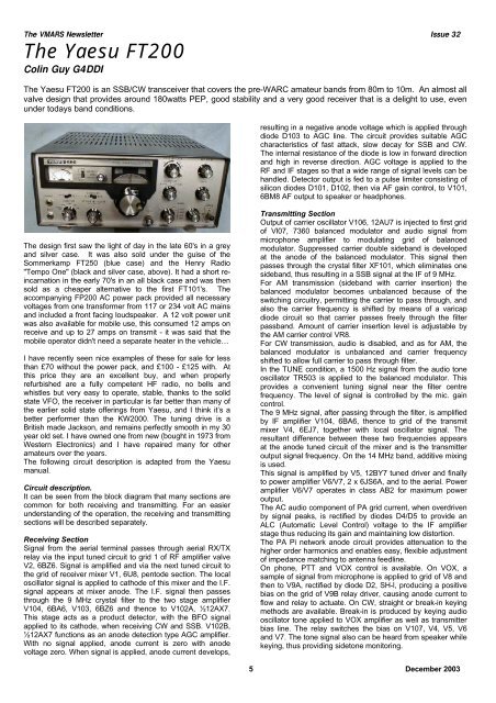
<strong>The</strong> VMARS Newsletter Issue 32<br />
<strong>The</strong> <strong>Yaesu</strong> <strong>FT200</strong><br />
Colin Guy G4DDI<br />
<strong>The</strong> <strong>Yaesu</strong> <strong>FT200</strong> is an SSB/CW transceiver that covers the pre-WARC amateur bands from 80m to 10m. An almost all<br />
valve design that provides around 180watts PEP, good stability and a very good receiver that is a delight to use, even<br />
under todays band conditions.<br />
resulting in a negative anode voltage which is applied through<br />
diode D103 to AGC line. <strong>The</strong> circuit provides suitable AGC<br />
characteristics of fast attack, slow decay for SSB and CW.<br />
<strong>The</strong> internal resistance of the diode is low in forward direction<br />
and high in reverse direction. AGC voltage is applied to the<br />
RF and IF stages so that a wide range of signal levels can be<br />
handled. Detector output is fed to a pulse limiter consisting of<br />
silicon diodes D101, D102, then via AF gain control, to V101,<br />
6BM8 AF output to speaker or headphones.<br />
<strong>The</strong> design first saw the light of day in the late 60's in a grey<br />
and silver case. It was also sold under the guise of the<br />
Sommerkamp FT250 (blue case) and the Henry Radio<br />
"Tempo One" (black and silver case, above). It had a short reincarnation<br />
in the early 70's in an all black case and was then<br />
sold as a cheaper alternative to the first FT101's. <strong>The</strong><br />
accompanying FP200 AC power pack provided all necessary<br />
voltages from one transformer from 117 or 234 volt AC mains<br />
and included a front facing loudspeaker. A 12 volt power unit<br />
was also available for mobile use, this consumed 12 amps on<br />
receive and up to 27 amps on transmit - it was said that the<br />
mobile operator didn't need a separate heater in the vehicle…<br />
I have recently seen nice examples of these for sale for less<br />
than £70 without the power pack, and £100 - £125 with. At<br />
this price they are an excellent buy, and when properly<br />
refurbished are a fully competent HF radio, no bells and<br />
whistles but very easy to operate, stable, thanks to the solid<br />
state VFO, the receiver in particular is far better than many of<br />
the earlier solid state offerings from <strong>Yaesu</strong>, and I think it’s a<br />
better performer than the KW2000. <strong>The</strong> tuning drive is a<br />
British made Jackson, and remains perfectly smooth in my 30<br />
year old set. I have owned one from new (bought in 1973 from<br />
Western Electronics) and I have repaired many for other<br />
amateurs over the years.<br />
<strong>The</strong> following circuit description is adapted from the <strong>Yaesu</strong><br />
manual.<br />
Circuit description.<br />
It can be seen from the block diagram that many sections are<br />
common for both receiving and transmitting. For an easier<br />
understanding of the operation, the receiving and transmitting<br />
sections will be described separately.<br />
Receiving Section<br />
Signal from the aerial terminal passes through aerial RX/TX<br />
relay via the input tuned circuit to grid 1 of RF amplifier valve<br />
V2, 6BZ6. Signal is amplified and via the next tuned circuit to<br />
the grid of receiver mixer V1, 6U8, pentode section. <strong>The</strong> local<br />
oscillator signal is applied to cathode of this mixer and the I.F.<br />
signal appears at mixer anode. <strong>The</strong> I.F. signal then passes<br />
through the 9 MHz crystal filter to the two stage amplifier<br />
V104, 6BA6, V103, 6BZ6 and thence to V102A, ½12AX7.<br />
This stage acts as a product detector, with the BFO signal<br />
applied to its cathode, when receiving CW and SSB. V102B,<br />
½12AX7 functions as an anode detection type AGC amplifier.<br />
With no signal applied, anode current is zero with anode<br />
voltage zero. When signal is applied, anode current develops,<br />
Transmitting Section<br />
Output of carrier oscillator V106, 12AU7 is injected to first grid<br />
of Vl07, 7360 balanced modulator and audio signal from<br />
microphone amplifier to modulating grid of balanced<br />
modulator. Suppressed carrier double sideband is developed<br />
at the anode of the balanced modulator. This signal then<br />
passes through the crystal filter XF101, which eliminates one<br />
sideband, thus resulting in a SSB signal at the IF of 9 MHz.<br />
For AM transmission (sideband with carrier insertion) the<br />
balanced modulator becomes unbalanced because of the<br />
switching circuitry, permitting the carrier to pass through, and<br />
also the carrier frequency is shifted by means of a varicap<br />
diode circuit so that carrier passes freely through the filter<br />
passband. Amount of carrier insertion level is adjustable by<br />
the AM carrier control VR8.<br />
For CW transmission, audio is disabled, and as for AM, the<br />
balanced modulator is unbalanced and carrier frequency<br />
shifted to allow full carrier to pass through filter.<br />
In the TUNE condition, a 1500 Hz signal from the audio tone<br />
oscillator TR503 is applied to the balanced modulator. This<br />
provides a convenient tuning signal near the filter centre<br />
frequency. <strong>The</strong> level of signal is controlled by the mic. gain<br />
control.<br />
<strong>The</strong> 9 MHz signal, after passing through the filter, is amplified<br />
by IF amplifier V104, 6BA6, thence to grid of the transmit<br />
mixer V4, 6EJ7, together with local oscillator signal. <strong>The</strong><br />
resultant difference between these two frequencies appears<br />
at the anode tuned circuit of the mixer and is the transmitter<br />
output signal frequency. On the 14 MHz band, additive mixing<br />
is used.<br />
This signal is amplified by V5, 12BY7 tuned driver and finally<br />
to power amplifier V6/V7, 2 x 6JS6A, and to the aerial. Power<br />
amplifier V6/V7 operates in class AB2 for maximum power<br />
output.<br />
<strong>The</strong> AC audio component of PA grid current, when overdriven<br />
by signal peaks, is rectified by diodes D4/D5 to provide an<br />
ALC (Automatic Level Control) voltage to the IF amplifier<br />
stage thus reducing its gain and maintaining low distortion.<br />
<strong>The</strong> PA Pi network anode circuit provides attenuation to the<br />
higher order harmonics and enables easy, flexible adjustment<br />
of impedance matching to antenna feedline.<br />
On phone, PTT and VOX control is available. On VOX, a<br />
sample of signal from microphone is applied to grid of V8 and<br />
then to V9A, rectified by diode D2, SH-l, producing a positive<br />
bias on the grid of V9B relay driver, causing anode current to<br />
flow and relay to actuate. On CW, straight or break-in keying<br />
methods are available. Break-in is produced by keying audio<br />
oscillator tone applied to VOX amplifier as well as transmitter<br />
bias line. <strong>The</strong> relay switches the bias on V107, V4, V5, V6<br />
and V7. <strong>The</strong> tone signal also can be heard from speaker while<br />
keying, thus providing sidetone monitoring.<br />
5 December 2003
<strong>The</strong> VMARS Newsletter Issue 32<br />
Bandswitched heterodyne oscillator<br />
This is a crystal oscillator using silicon type 2SC372<br />
transistor, and it is operative on bands 7, 21 and 28 MHz.<br />
VFO<br />
<strong>The</strong> VFO is a transistorised Colpitts circuit with 25C372<br />
oscillator and 25C372 buffer. It has linear tuning over the<br />
range 5 to 5.5 MHz. A passband filter circuit at output is tuned<br />
to pass the 5-5.5 MHz range. Varicap diode D401, 1S145<br />
permits receiver off-set tuning (clarifier) of ±5 kHz on receive.<br />
Crystal calibrator oscillator<br />
Transistor oscillator 2SC367 with 100 kHz crystal, and diode<br />
type 1S1007 harmonic generator provides accurate check<br />
points every 100 kHz on main dial.<br />
<strong>The</strong> FP200 AC Power supply<br />
Oscillator circuits<br />
In the FT-200 crystal oscillators are used for carrier<br />
generation and the bandswitched heterodyne oscillator,<br />
together with a self-controlled oscillator for the VFO, which is<br />
at a frequency low enough to obtain good stability. Other<br />
oscillators included are 100 kHz crystal calibrator and audio<br />
tone oscillator. An external VFO model FV-200 is available to<br />
provide additional operational flexibility and split frequency<br />
operation:<br />
Carrier crystal oscillator<br />
V106, 12AU7 double triode with crystals 8998.5 kHz and<br />
9001.5 kHz, one in each triode section. With sideband<br />
selector switch at NORMAL, carrier crystal 8998.5 is operative<br />
for 7 and 14 MHz band and 9001.5 for 3.5, 21 and 28 MHz.<br />
When the selector switch is in REVERSE position, then the<br />
carrier crystal oscillator sections are changed. <strong>The</strong> carrier<br />
oscillator is used as a BFO when in receive mode.<br />
On AM & CW, crystal 9001.5 is used and its frequency is<br />
lowered 200 Hz by diode switch D104, 1S1007, bringing the<br />
carrier into the filter passband.<br />
AF oscillator<br />
A phase shift oscilator using a 25C372 transistor, generating<br />
an audio tone signal at 1500 Hz, supplies transmitter tune-up<br />
signal and CW sidetone monitoring. This oscillator also<br />
actuates the VOX relays for semi-automatic break-in CW<br />
operation.<br />
Local oscillator mixer circuit<br />
<strong>The</strong> VFO output is applied to grid 1 of V3, 6CB6 mixer and the<br />
heterodyne oscillator output to its cathode. <strong>The</strong> resultant beat<br />
frequency is selected in the anode tuned circuit.<br />
Meter circuit<br />
<strong>The</strong> meter is a 1 mA movement, and it is connected to 2nd IF<br />
stage to read the change in cathode voltage of V 103,<br />
resulting from variations of AGC voltage, to indicate receiver<br />
"S" units.<br />
<strong>The</strong> meter is automatically switched by relay RL101, on<br />
transmit, to indicate relative power output (P0) PA cathode<br />
current (IC) and ALC voltage. Meter scale is fully calibrated,<br />
and the transmitter metering functions P0, IC and ALC, are<br />
selected by panel mounted slide switch.<br />
Voltage regulator circuit<br />
<strong>The</strong> voltage regulator circuit, mounted on a print board,<br />
provides 9 volts for all transistor oscillators, the supply for this<br />
is derived from the +150V HT rail via a large 5KΩ resistor.<br />
Two transistors are used, 2SC372 and 2SC367, together with<br />
two zener diodes, 1S331 and 1S336, and voltage level can be<br />
set by adjustment of variable resistor VR501.<br />
Mixing sequence<br />
<strong>The</strong> 5 - 5.5 MHz VFO is mixed with the signal frequency on<br />
80m, (3.5 - 4MHz) to give the 9MHz IF by addition, and on<br />
20m (14 - 14.5MHz) by subtraction. On 40m the VFO is<br />
premixed with the bandswitched oscillator at 11MHz to give<br />
16 - 16.5MHz, the signal frequency (7 - 7.5MHz) is subtracted<br />
to give the 9MHz IF. On 15m the VFO is premixed with<br />
35.5MHz to give 30 to 30.5MHz, again subtracting the signal<br />
frequency (21 - 21.5MHz) gives the 9MHz IF. On 10m the<br />
premix frequencies are 42.5MHz, 43.0MHz, 43.5MHz and<br />
44.0MHz to give ranges of 28 - 28.5MHz, 28.5 - 29MHz, 29 -<br />
29.5MHz and 29.5 - 30MHz respectively.<br />
Accessory Socket<br />
An accessory socket is provided for an external transverter<br />
etc. If no accessory is connected, a plug must be inserted with<br />
a link between pin 1 and 2 to supply heater voltage to the PA<br />
valves. <strong>The</strong> same applies to the external VFO socket.<br />
<strong>FT200</strong> Top View<br />
Power supply<br />
<strong>The</strong> <strong>FT200</strong> requires a 12 volt AC supply for the valve heaters,<br />
which also supplies the relays via an internal rectifier, 150V<br />
DC and 300V DC for the valve anodes, 600V DC for the PA<br />
6 December 2003
<strong>The</strong> VMARS Newsletter Issue 32<br />
and –100 V DC bias supply. All of these are supplied from<br />
the FP200 AC supply unit or the DC200 12 volt supply unit.<br />
None of the supplies require to be stabilised, and it would not<br />
be difficult to concoct a psu from a number of transformers if<br />
you aquire a set without a psu, or with one that is burnt out.<br />
<strong>The</strong> power and accessory socket (both 11 pin “octal” types)<br />
connections are shown in the diagrams at the end of the<br />
article.<br />
Construction<br />
<strong>The</strong> IF, tx and rx audio stages and tx mixer are all on a large<br />
pcb, this can be seen in the underside view below. <strong>The</strong><br />
underside of the pcb is easily accessible for repair and should<br />
present few problems. Smaller pcb’s carry the 9 volt regulator<br />
and tone oscillator, the 100kHz crystal calibrator and the<br />
bandswitched heterodyne oscillator. <strong>The</strong>se are all mounted<br />
on a conventional steel chassis, the receiver RF stages,<br />
transmitter mixer, driver and PA and vox amplifier are all<br />
directly mounted on the chassis and conventionally wired.<br />
<strong>The</strong> chassis and vertically mounted front panel can be<br />
extracted from the “wraparound” steel case by removing five<br />
screws from the underside. Once removed virtually everything<br />
is accessible for repair.<br />
(C103, 0.01µF), leaky or shorted cathode decoupling<br />
electrolytic (C101, 30µF 15V) or leakage in the valve itself. All<br />
of these cause the valve to run even hotter than normal with<br />
no apparent effect on performance, but it has the the result<br />
that the pcb cooks to a cinder. In this case a prod of the valve<br />
will show that it is hanging in there only by the copper tracks!<br />
Both of these faults can be repaired, but it is worth looking,<br />
and allowing for in the purchase price. Also look at the RF<br />
section trimmers (visible through the holes in the bottom of<br />
the case) to see if they have been “twiddled” – ham-fisted<br />
adjustment of these can cause other problems – see below –<br />
and realignment is not a task to be taken lightly.<br />
Other faults. Not uncommon is an apparent lack of AGC<br />
action, with the receiver seeming insensitive and little<br />
movement of the s-meter even on very strong signals. This is<br />
usually because of grid leakage in one or other of the IF<br />
valves (V103, 6BZ6, V104 6BA6) upsetting the slightly<br />
unusual agc circuitry. Substitution is the best way of<br />
determining this.<br />
A noisy bandswitch is not uncommon, lack of sensitivity on<br />
one band usually being traceable to this area. Do not be<br />
tempted to spray the switch with switch cleaner whilst the set<br />
is powered though, it can cause the wafers to arc as some<br />
carry full HT, and replacement would be a serious job. Give<br />
the switches a spray with the power off, work the switch a few<br />
times then allow to dry before applying power. “Super<br />
Servisol” is recommended for this job, don’t be tempted to use<br />
WD40!<br />
Total failure of one band can be caused by an open – circuit<br />
coil in the receiver RF or pre-mixer stages – these are all<br />
common to transmit and receive. What happens here is that<br />
the valve anode voltage is supplied via the coil and the tuning<br />
gang and trimmer are connected from the anode to earth, so<br />
the HT voltage is across both, a short in the gang section or<br />
the trimmer, caused by stray metal particles or inept handling<br />
burns out the coil.<br />
Remember that a jumper plug must be in the accessory<br />
socket – if you have no transmit output look to see if the PA<br />
valve heaters are alight!<br />
<strong>FT200</strong> underside view<br />
What to look for when buying one.<br />
Considering the amount of heat these sets generate they are<br />
extremely reliable, there are, however, as with just about any<br />
piece of equipment, a few weak spots. Undoubtedly the most<br />
common fault is failure of the pa grid coupling capacitor C55,<br />
shown in the manual as 100pF 1kV, but I have frequently<br />
found 500 volt specimens fitted here. <strong>The</strong>re is 300 volts on<br />
one side of it from the driver anode and minus 150 volts the<br />
other, plus several tens of volts of RF on transmit so it<br />
obviously has a hard time. Failure not only removes the<br />
negative grid bias on the PA valves, but applies a positive<br />
bias to them. Not unnaturally this results in the rapid demise<br />
of the valves, which are now expensive and quite difficult to<br />
obtain, and can also result in the destruction of the mains<br />
transformer (protected only by a single primary fuse, often<br />
replaced with one of a higher rating!) if the owner wasn't there<br />
to switch the set off very quickly when it showed the obvious<br />
signs of distress. <strong>The</strong> FT101 and 901 also suffered from this<br />
problem. <strong>The</strong>refore, a good look at the PA valves is essential,<br />
and if you are offered a power unit with it, a close look (and<br />
sniff) at the transformer is worthwhile.<br />
Another area worth a look is around the receiver audio output<br />
valve (V101, 6BM8) which is mounted on the main printed<br />
circuit board. This can suffer from any of the usual afflictions<br />
of a triode - pentode AF amplifier - leaky coupling capacitor<br />
Valves<br />
<strong>The</strong> only valve that is really scarce today is the 7360 balanced<br />
modulator, but I’ve never known an instance of failure of<br />
these, so as long as your set has one, and it isn’t broken there<br />
should be no problem. <strong>The</strong> PA valves, 6JS6, can still be<br />
obtained in matched pairs though expensive. <strong>The</strong>se do seem<br />
to lose emission over time, this probably happens if the set is<br />
used for long periods of receiving and little transmitting, as the<br />
heater remains on all the time, there is no facility to switch<br />
them off as there is with the FT101 etc. All of the other types<br />
are fairly common and easily obtainable. <strong>The</strong> table below<br />
shows the complete valve list, with British equivalents where<br />
known.<br />
V1 6U8, ECF82<br />
V2 6BZ6<br />
V3 6CB6<br />
V4 6EJ7<br />
V5 12BY7A<br />
V6 6JS6A<br />
V7 6JS6A<br />
V8 6AV6<br />
V9 12AU7, ECC82<br />
V101 6BM8, ECL82<br />
V102 12AX7, ECC83<br />
V103 6BZ6<br />
V104 6BA6, EF93<br />
V105 12AX7, ECC83<br />
V106 12AU7, ECC82<br />
V107 7360<br />
<strong>FT200</strong> Valve lineup<br />
7 December 2003
<strong>The</strong> VMARS Newsletter Issue 32<br />
<strong>The</strong> <strong>FT200</strong> Block diagram.<br />
Semiconductors<br />
<strong>The</strong>re are no exotic semiconductors or unobtainable IC's (as<br />
there is with the FT101!) All of the transistors are small signal<br />
NPN types and should be easily replaceable if necessary,<br />
though I've never known one to fail. <strong>The</strong> numerous diodes<br />
shouldn't present a problem, the only ones I've had trouble<br />
with have been the power supply rectifiers, which can be<br />
replaced by easily available BY227, 1N4007 etc.<br />
Microphone socket<br />
A ¼ inch stereo jack plug is used for the microphone, slightly<br />
unusually the tip is the ptt connection and the ring is the mic<br />
live. <strong>The</strong> sleeve is of course earth.<br />
Alignment<br />
CAUTION —Before any work is attempted, remember that<br />
high voltages are employed in this equipment, so —TAKE<br />
CARE!<br />
Equipment required:<br />
VTVM with RF probe<br />
RF standard signal generator<br />
AF signal generator<br />
Frequency meter<br />
Dummy load 50 ohms<br />
Suitable alignment tools<br />
Voltage regulator<br />
<strong>The</strong> V.R. is mounted on a printed circuit board and supplies a<br />
regulated output of 9V, adjustable by the pre-set type<br />
miniature pot VR501. If output cannot be brought up to the<br />
9V, level it may be due to a fault in components on the printed<br />
circuit board, e.g. transistors or zener diode, or supply voltage<br />
below 11V.<br />
Use frequency meter for alignment, although this can be<br />
done, with care, if beats are heard every 100 kHz using the<br />
crystal calibrator.<br />
Coarse alignment is by adjustment of trimmer TC401.<br />
<strong>The</strong> piston type trimmer TC402 is for adjustment of<br />
temperature compensation. If turned clockwise, then<br />
compensation becomes greater. If TC402 is adjusted, then<br />
TC401 must be re-adjusted to maintain calibration.<br />
For precise adjustment of dial linearity, careful adjustment (by<br />
bending) of end rotor plates of main tuning condenser is<br />
necessary.<br />
VFO injection to grid 1 of V3, 6CB6 should be 0.5V or more<br />
over full VFO range, measured with VTVM and RF probe. To<br />
obtain the same frequency of clarifier at "0" as at ”OFF'',<br />
adjust VR7.<br />
Heterodyne crystal oscillator<br />
Apply RF probe to Pin 2 of V3, and with bandswitch at 28.5,<br />
adjust L202 for maximum meter reading. On 21 MHz band<br />
adjust TC202. On 7 MHz band adjust TC201. If optional 10<br />
meter range crystals are fitted, adjust appropriate trimmer<br />
condensers for 10 meter crystals.<br />
100 kHz calibrator Adjust frequency with TC301 by checking<br />
against WWV, with aid of separate receiver.<br />
Pre-mixer (VFO mixer) This is V3, with output anode tuned<br />
circuit to select the resultant beat of VFO and heterodyne<br />
oscillator (or VFO frequency in case of 3.5 and 14 MHz<br />
bands). This alignment should be carefully done as other<br />
frequencies can appear at output, VFO, etc. This alignment is<br />
explained in transmitter alignment section. Refer to chart,<br />
below, for correct output frequencies.<br />
VFO alignment<br />
On the red scale, "0”=5 MHz and "500" = 5.5 MHz<br />
Switch off crystal heterodyne oscillator by placing bandswitch<br />
on 3.5 or 14 MHz band. Set the receiver offset tuning OFF.<br />
8 December 2003
<strong>The</strong> VMARS Newsletter Issue 32<br />
Balanced modulator<br />
Band Mixed Frequency<br />
Function switch to TUNE, meter to P.O., tune transmitter for<br />
maximum reading. (Keep IC down by use of MIC gain).<br />
3.5 5 – 5.5 MHz<br />
Now function to SSB, MIC gain to zero, and adjust VR106 for<br />
7.0 16 – 16.5 MHz<br />
minimum reading. For most sensitive indication, connect RF<br />
14.0 5 – 5.5 MHz<br />
probe to dummy load, or use another receiver and observe its<br />
S-meter reading.<br />
21.0 30 – 30.5 MHz<br />
<strong>The</strong>n switch to opposite sideband position, and readjust<br />
28.0 37.0 – 37.5 MHz<br />
VR106. Repeat several times for best result. If there is a<br />
28.5 37.5 – 38 MHz<br />
marked difference between the two positions, then adjustment<br />
of carrier oscillator or crystal filter may be required.<br />
29.0 38 – 38.5 MHz<br />
29.5 38.5 – 39 MHz<br />
Crystal filter<br />
<strong>The</strong> filter is aligned once in receiver alignment, but further<br />
V3 anode alignment frequencies<br />
alignment in this section (transmitting) is necessary.<br />
At the TUNE position adjust L103, L104 and L105 for<br />
maximum output. Keep drive reduced to a fairly low level for<br />
AGC<br />
the most accurate determination of the maximum peak. In<br />
Set function switch to AM, RF gain maximum, then S-meter order to examine filter characteristics, set function to SSB and<br />
should read "0" with the aerial socket shorted. Set VR102 connect an A.F. generator to MIC jack, then take a curve of<br />
(AGC adjust) so that it is at a point just before the S-meter the A.F. response (in effect, the filter passband), by plotting<br />
needle commences to rise above "0". Now adjust the meter between 300-2500 Hz. If output level changes no more than 3<br />
sensitivity control so that with 50mV applied to the aerial dB, then it is OK. Repeat on reverse sideband. If the two<br />
socket from the signal generator the meter reads S9. Now set curves do not match, then a slight adjustment of each carrier<br />
function switch to SSB, short out antenna socket, and meter crystal frequency is necessary to bring the two curves<br />
should read "0"; but if not, then adjust the compensation together In their frequency limits. If carrier is too close to 9000<br />
capacitance (C165) between pin 2 and pin 8 of V102 to make kHz filter centre frequency, then high audio frequencies will be<br />
meter read minimum deflection.<br />
attenuated. If carrier is too far removed, then low frequencies<br />
will be attenuated. Carrier frequency adjustment is by TC101<br />
and TC102.<br />
I.F. amplifier<br />
Connect signal generator at 9,000 kHz and adjust tuning for<br />
maximum S-meter reading at centre of filter passband by<br />
observing S-meter at same time as tuning signal generator<br />
frequency. Now adjust L101, L102, L103, L104 for maximum<br />
meter reading.<br />
Receiver mixer<br />
This is V16U8 (alternative types 6EA8, 6GH8). Connect RF<br />
probe to pin 8, cathode of triode section, and adjust grid<br />
tuning. Oscillator injection should read greater than 0.5V on<br />
every band. Adjust trap coil L22 for minimum beat at 21.3 MC.<br />
This adjustment should occur within one turn of the core slug.<br />
L1 is trap coil for 3.5 and 14 MC bands and should be<br />
adjusted so that no oscillation occurs in these bands. Use a<br />
plastic alignment tool so that no damage will result to the<br />
internal hexagon type slugs.<br />
RF amplifier<br />
Connect signal generator to aerial socket. On 3.5 MHz band<br />
set VFO to "0" on black scale and GRID to second point up<br />
from its anticlockwise position. Apply 3500 kHz signal and<br />
adjust L7 and L12 for maximum S-meter reading. Use plastic<br />
alignment tool. 7 MHz band, VFO to "0" on red scale, GRID at<br />
same point as for 3.5 MHz, signal generator at 7000 kHz.<br />
Adjust TC1 and TC2 for maximum.<br />
14 MC band, VFO to 250, GRID at centre position, signal<br />
generator at 14250 kHz. Adjust L10 and L15 for maximum.<br />
21 MHz band, VFO to 250, GRID at centre, signal generator<br />
at 21250 kHz. Adjust L9 and L14 for maximum.<br />
28.5 MHz band, VFO to 500, GRID at centre, signal generator<br />
at 29,000 kHz. Adjust L3, L8 and L13 for maximum.<br />
On 7 MC band, VFO to 500, apply 9 MC signal of sufficient<br />
level to give an S-meter reading; then adjust L2 for minimum<br />
dip in S-meter reading.<br />
Transmitter Alignment<br />
<strong>The</strong> transmitter uses many common receiver circuits;<br />
therefore it is necessary to first correctly align the receiver<br />
section. A 50-75 ohms dummy load must be used on the<br />
transceiver during transmitter alignment. Take care to avoid<br />
touching high voltage points!<br />
Driver stage<br />
Set up transmitter on TUNE, but keep level down to safe limit<br />
by adjustment of MIC gain control; then adjust driver coils and<br />
trimmer condensers for peak in output, as in receiver section<br />
alignment.<br />
Final Amplifier Neutralisation<br />
When replacing the final amplifier valves, it may be necessary<br />
to reset the bias to give correct idle current and check<br />
neutralisation. Using the procedure outlined below will<br />
guarantee maximum output and long tube life.<br />
CAUTION HIGH VOLTAGES ARE PRESENT ON<br />
UNDERSIDE OF CHASSIS AND INSIDE OF FINAL<br />
COMPARTMENT. USE GREAT CARE WHILE MAKING<br />
ADJUSTMENTS WITH WIRING EXPOSED.<br />
Connect a dummy load to antenna, and set meter to IC.<br />
(cathode current.) Locate TC3, the neutralisation variable<br />
capacitor shaft in the final amplifier compartment. Check final<br />
amplifier idle current in USB or LSB position and adjust as<br />
described before.<br />
Tune up the transceiver at 21.5 MHz, with MODE switch set<br />
to AM position, and advance CARRIER potentiometer or the<br />
rear panel until meter IC reads 150mA<br />
Rotate PLATE tuning control and observe dip as indicated on<br />
the meter.<br />
If the dip is not prominent, reduce loading control slightly for<br />
better indication. As the PLATE control is rotated the meter<br />
should rise equally and smoothly on either side of maximum<br />
dip indication.<br />
Determine which side of the dip rises abruptly. Set PLATE<br />
control slightly to this side of dip keeping the meter reading<br />
below 150 mA.<br />
Using an insulated trimming tool, rotate the neutralisation<br />
capacitor shaft very slightly in the direction which reduces the<br />
current shown on the meter. Repeat steps 6 and 7 until the<br />
meter indicates a smooth and equal rise on either side of the<br />
maximum dip point.<br />
<strong>The</strong> final compartment cover must be in place to supply the<br />
RF shielding required during the neutralisation procedure.<br />
9 December 2003
<strong>The</strong> VMARS Newsletter Issue 32<br />
Operation<br />
<strong>The</strong> transceiver is controlled by a three position lever switch<br />
which is marked "oper", "rec" and "cal". In the "rec" position<br />
the transmitter is disabled. Receiver operation is a simple as<br />
selecting your band and mode, and peaking the "Grid" control<br />
for maximum. Moving the switch to "oper" will put the<br />
transceiver into the transmit condition. If the mode switch in<br />
"tune", the carrier output can be controlled with the mic gain<br />
control, apply the minimum necessary to produce some<br />
output then dip the PA current in the normal way, keeping it<br />
below 150mA. If the mode switch is in CW, transmission is<br />
controlled by the key, and on SSB or AM, transmission is<br />
controlled by the PTT switch. Note that on SSB or AM, if the<br />
mic is unplugged the set will go to transmit immediately.<br />
<strong>The</strong> PA is tuned up in the normal way with the mode switch in<br />
the "tune" position, but care should be taken that it is coupled<br />
into as near as 50W as possible, the loading capacitor is very<br />
closely spaced and prone to arcing.<br />
Accessory socket connections<br />
1. 6JS6A Heater 8. Earth<br />
2. 12.6V Heater supply 9. Relay close on tx<br />
3. +150V 10. Relay common<br />
4. +300V 11. Relay close on<br />
rx<br />
5. +600V<br />
6. –100V<br />
7. ALC input.<br />
Power socket connections<br />
1. –100V<br />
2. Earth<br />
3. +300V<br />
4. +600V<br />
5. Heater common<br />
6. Heater 12.6V Rx<br />
7. Speaker<br />
8. Heater 12.6V Tx<br />
9. Power switch<br />
10. Power switch<br />
11. +150V<br />
Conclusion<br />
This is a highly useable radio that can be obtained quite<br />
cheaply, is generally easy to repair, and whose performance<br />
meets modern standards if properly set up. <strong>The</strong> only real<br />
downside of it is that it lacks topband (and the other "WARC"<br />
bands), the AM performance is poor - the filter is too narrow<br />
for receive, and the transmit quality is poor, being in reality<br />
SSB with reinserted carrier, and it takes some juggling with<br />
the mic gain and carrier level to get acceptable results.<br />
Performance on SSB and CW is excellent, drift is minimal<br />
after about 10 minutes warmup, and the controls are few and<br />
mostly intuitive to use. On - air reports on SSB are always<br />
good and the receiver has a very low background noise level,<br />
no noticeable sproggies, even on 40m, and sounds excellent.<br />
<strong>The</strong>re is not room to print the full circuit diagram in the<br />
newsletter, it spreads across four pages, but if anyone needs<br />
a copy please contact the author.<br />
<strong>The</strong> FP 200 power supply circuit<br />
10 December 2003