QUASAR ELECTRONICS KIT No. 1028 4 Watt FM TRANSMITTER
QUASAR ELECTRONICS KIT No. 1028 4 Watt FM TRANSMITTER
QUASAR ELECTRONICS KIT No. 1028 4 Watt FM TRANSMITTER

You also want an ePaper? Increase the reach of your titles
YUMPU automatically turns print PDFs into web optimized ePapers that Google loves.
<strong>QUASAR</strong> <strong>ELECTRONICS</strong> <strong>KIT</strong> <strong>No</strong>. <strong>1028</strong><br />
4 <strong>Watt</strong> <strong>FM</strong> <strong>TRANSMITTER</strong><br />
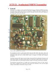
General Description<br />
This is a small but powerful <strong>FM</strong> transmitter having three RF stages incorporating an audio<br />
preamplifier for better modulation. It has an output power of 4 <strong>Watt</strong>s and works off 12-18<br />
VDC which makes it easily portable. It is the ideal project for the beginner who wishes to<br />
get started in the fascinating world of <strong>FM</strong> broadcasting and wants a good basic circuit to<br />
experiment with.<br />
Technical Specifications - Characteristics<br />
Modulation type: ........ <strong>FM</strong><br />
Frequency range: .... 88-108 MHz<br />
Working voltage: ..... 12-18 VDC<br />
Maximum current: ....... 450 mA<br />
Output power: ............ 4 W<br />
How it Works<br />
As it has already been mentioned the transmitted signal is Frequency Modulated (<strong>FM</strong>)<br />
which means that the carrier’s amplitude stays constant and its frequency varies according<br />
to the amplitude variations of the audio signal. When the input signal’s amplitude increases<br />
(i.e. during the positive half cycles) the frequency of the carrier increases too, on the other<br />
hand when the input signal decreases in amplitude (negative half-cycle or no signal) the<br />
carrier frequency decreases accordingly. In figure 1 you can see a graphic representation<br />
of Frequency Modulation as it would appear on an oscilloscope screen, together with the<br />
modulating AF signal. The output frequency the transmitter is adjustable from 88 to 108<br />
MHz which is the <strong>FM</strong> band that is used for radio broadcasting. The circuit as we have<br />
already mentioned consists of four stages. Three RF stages and one audio preamplifier for<br />
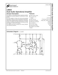
the modulation. The first RF stage is an oscillator and is built around TR1. The frequency<br />
of the oscillator is controlled by the LC network L1-C15. C7 is there to ensure that the<br />
circuit continues oscillating and C8 adjusts the coupling between the oscillator and the<br />
next RF stage which is an amplifier. This is built around TR2 which operates in class C<br />
and is tuned by means of L2 and C9. The last RF stage is also an amplifier built around<br />
TR3 which operates in class C the input of which is tuned by means of C10 and L4. From<br />
the output of this last stage which is tuned by means of L3-C12 is taken the output signal<br />
which through the tuned circuit L5-C11 goes to the aerial.<br />
The circuit of the preamplifier is very simple and is built around TR4. The input sensitivity<br />
of the stage is adjustable in order to make it possible to use the transmitter with different<br />
input signals and depends upon the setting of VR1. The transmitter can be modulated<br />
directly with the piezoelectric microphone supplied, a small cassette recorder, etc. It is of
course possible to use of our audio mixers in the input for more professional results.<br />
Construction<br />
First of all let us consider a few basics in building electronic circuits on a printed circuit<br />
board. The board is made of a thin insulating material clad with a thin layer of conductive<br />
copper that is shaped in such a way as to form the necessary conductors between the<br />
various components of the circuit. The use of a properly designed printed circuit board is<br />
very desirable as it speeds construction up considerably and reduces the possibility of<br />
making errors. <strong>QUASAR</strong> <strong>ELECTRONICS</strong> Kit boards also come pre-drilled and with the<br />
outline of the components and their identification printed on the component side to make<br />
construction easier. To protect the board during storage from oxidation and assure it gets<br />
to you in perfect condition the copper is tinned during manufacturing and covered with a<br />
special varnish that protects it from getting<br />
oxidised and also makes soldering easier. Soldering the components to the board is the<br />
only way to build your circuit and from the way you do it depends greatly your success or<br />
failure. This work is not very difficult and if you stick to a few rules you should have no<br />
problems. The soldering iron that you use must be light and its power should not exceed<br />
the 25 <strong>Watt</strong>s. The tip should be fine and must be kept clean at all times. For this purpose<br />
come very handy specially made sponges that are kept wet and from time to time you can<br />
wipe the hot tip on them to remove all the residues that tend to accumulate on it.<br />
DO NOT file or sandpaper a dirty or worn out tip. If the tip cannot be cleaned,<br />
replace it. There are many different types of solder in the market and you should choose a<br />
good quality one that contains the necessary flux in its core, to assure a perfect joint every<br />
time.<br />
DO NOT use soldering flux apart from that which is already included in your solder. Too<br />
much flux can cause many problems and is one of the main causes of circuit malfunction.<br />
If nevertheless you have to use extra flux, as it is the case when you have to tin copper<br />
wires, clean it very thoroughly after you finish your work. In order to solder a component<br />
correctly you should do the following:<br />
- Clean the component leads with a small piece of emery paper.<br />
Bend them at the correct distance from the component’s body and insert the component in<br />
its place on the board.<br />
- You may find sometimes a component with heavier gauge leads than usual, that are too<br />
thick to enter in the holes of the p.c. board. In this case use a mini drill to enlarge the holes<br />
slightly.<br />
- Do not make the holes too large as this is going to make soldering difficult afterwards.<br />
- Take the hot iron and place its tip on the component lead while holding the end of the<br />
solder wire at the point where the lead emerges from the board. The iron tip must touch<br />
the lead slightly above the p.c. board. - When the solder starts to melt and flow wait till it<br />
covers evenly the area around the hole and the flux boils and gets out from underneath the<br />
solder. The whole operation should not take more than 5 seconds. Remove the iron and<br />
allow the solder to cool naturally without blowing on it or moving the component. If<br />
everything was done properly the surface of the joint must have a bright metallic finish and<br />
its edges should be smoothly ended on the component lead and the board track. If the<br />
solder looks dull, cracked, or has the shape of a blob then you have made a dry joint and<br />
you should remove the solder (with a pump, or a solder wick) and redo it.<br />
- Take care not to overheat the tracks as it is very easy to lift them from the board and<br />
break them.
- When you are soldering a sensitive component it is good practice to hold the lead from<br />
the component side of the board with a pair of long-nose pliers to divert any heat that<br />
could possibly damage the component.<br />
- Make sure that you do not use more solder than it is necessary as you are running the<br />
risk of short-circuiting adjacent tracks on the board, especially if they are very close<br />
together.<br />
- When you finish your work cut off the excess of the component leads and<br />
clean the board thoroughly with a suitable solvent to remove all flux residues that may still<br />
remain on it.<br />
This is an RF project and this calls for even more care during soldering as sloppiness<br />
during construction can mean low or no output at all, low stability and other problems.<br />
Make sure that you follow the general rules about electronic circuit construction outlined<br />
above and double-check everything before going to the next step. All the components are<br />
clearly marked on the component side of the P.C. board and you should have no difficulty<br />
in locating and placing them. Solder first of all the pins, and continue with the coils taking<br />
care not to deform them, the RFC’s, the resistors, the capacitors and finally the electrolytic<br />
and the trimmers. Make sure that the electrolytic are correctly placed with respect to their<br />
polarity and that the trimmers are not overheated during soldering. At this point stop for a<br />
good inspection of the work done so far and if you see that everything is OK go on and<br />
solder the transistors in their places taking grate care not to overheat them as they are the<br />
most sensitive of all the components used in the project. The audio frequency input is at<br />
points 1 (ground) and 2 (signal), the power supply is connected at points 3 (-) and 4 (+)<br />
and the antenna is connected at points 5 (ground) and 6 (signal). As we have already<br />
mentioned the signal you use for the modulation of the transmitter could be the output of a<br />
preamplifier or mixer or in case you only want to modulate it with voice you can use the<br />
piezoelectric microphone supplied with the Kit. (The quality of this microphone is not very<br />
good but it is quite adequate if you are interested in speech only.) As an antenna you can<br />
use an open dipole or a Ground Plane. Before you start using the transmitter for the first<br />
time and every time you change its working frequency you must follow the procedure<br />
described below which is called alignment.<br />
Adjustments<br />
If you expect your transmitter to be able to deliver its maximum output at any time you<br />
must align all the RF stages in order to ensure that you get the best energy transfer<br />
between them. There are two ways to do this and it depends if you have a SWR meter or<br />
not which method you are going to follow. If you have a SWR meter turn the transmitter<br />
on, having connected the SWR meter in its output in series with the antenna, and turn C15<br />
in order to tune the oscillator to the frequency you have chosen for your broad casts. Then<br />
start adjusting the trimmers C8,9,10,12 and 11 in this order till you get the maximum<br />
output power in the SWR meter. For those who don’t have a SWR meter there is another<br />
method which gives quite satisfactory results. You only have to build the little circuit in Fig.<br />
2 which is connected in the out put of the transmitter and in its output (across C16) you<br />
connect your multi-tester having selected a suitable VOLTS scale. You tune C15 in the<br />
desired frequency and then adjust the other trimmers in the same order as it is described<br />
above for the maximum output in the multimeter. The disadvantage of this method is that<br />
you do not align the transmitter with a real antenna connected in its output and it may be<br />
necessary to make slight adjustments to C11 and C12 for a perfect antenna match.
Do not forget to align your transmitter every time you change your aerial or your working<br />
frequency.<br />
WARNING: In every transmitter there are present apart from the main output frequency<br />
various harmonics that usually have a very short range. In order to make sure you haven’t<br />
tuned on one of them do the tuning as far as possible from your receiver, or use a<br />
Spectrum Analyser to see your output spectrum and make sure that you tune your<br />
transmitter on the right frequency.<br />
Warning<br />
<strong>QUASAR</strong> <strong>ELECTRONICS</strong> kits are sold as stand alone training kits.<br />
If they are used as part of a larger assembly and any damage is caused, our company<br />
bears no responsibility.<br />
While using electrical parts, handle power supply and equipment with great care, following<br />
safety standards as described by international specs and regulations.<br />
CAUTION<br />
All the RF kits are sold for experimental and laboratory use only. Their possession and use<br />
are limited by laws which vary from state to state. Please get information about what you<br />
can or can not do in your area and stay within the legal limits. Make sure you do not<br />
become a nuisance to others with your experiments. <strong>QUASAR</strong> <strong>ELECTRONICS</strong> Kit has no<br />
responsibility whatsoever for any misuse of its products.<br />
If it does not work<br />
- Check your work for possible dry joints, bridges across adjacent tracks or soldering flux<br />
residues that usually cause problems.<br />
Check again all the external connections to and from the circuit to see if there is a mistake<br />
there.<br />
- See that there are no components missing or inserted in the wrong places.<br />
- Make sure that all the polarised components have been soldered the right way round.<br />
- Make sure that the supply has the correct voltage and is connected the right way round<br />
to your circuit.<br />
- Check your project for faulty or damaged components.<br />
If your project still fails to work, please contact us for information about our Get-You-Going<br />
service.
Electronic Diagram.<br />
Parts List<br />
All components including printed circuit board, assembly instructions including schematics<br />
and detailed parts list are supplied when you purchase the kit.<br />
Ordering<br />
For pricing info and online ordering please visit:<br />
http://www.quasarelectronics.com/<strong>1028</strong>.htm<br />
For further info please contact us by e-mail:<br />
mailto: sales@QuasarElectronics.com<br />
COPYRIGHT © 2003 Quasar Electronics Limited. All rights reserved. Reproduction of this document in<br />
whole or in part in any form or medium without express written permission of Quasar Electronics Limited is<br />
prohibited.<br />
E&OE