10 Watt Stereo Audio Amplifier (Code 3143) - Quasar Electronics
10 Watt Stereo Audio Amplifier (Code 3143) - Quasar Electronics
10 Watt Stereo Audio Amplifier (Code 3143) - Quasar Electronics

Create successful ePaper yourself
Turn your PDF publications into a flip-book with our unique Google optimized e-Paper software.
6 – <strong>10</strong> <strong>Watt</strong> <strong>Stereo</strong> <strong>Audio</strong> <strong>Amplifier</strong> (<strong>Code</strong> <strong>3143</strong>)<br />
K<br />
it <strong>3143</strong> is a class AB stereo audio power<br />
amplifier designed for quality hi-fi<br />
applications using a TDA2005 module. It is<br />
easy to construct and has a minimum of<br />
external components. The module has output<br />
current protection and thermal protection. This<br />
is the data book circuit which produces an<br />
excellent sound. The supply voltage required<br />
for this kit is 8 - 18V DC at 1 to 2 Amps.<br />
Maximum output power will only be obtained<br />
with a power supply of at least 2A at 15V DC,<br />
and using 2 Ohm speakers (or 2 by 4 Ohm<br />
speakers in parallel). However approximately<br />
4W per channel can be obtained with only a<br />
15V DC, 1A supply into 4 ohm loads.<br />
The power supply should be well filtered to<br />
reduce mains hum, the on board capacitors<br />
alone are not adequate for this purpose but are<br />
necessary to ensure stability. Extra filtering is<br />
unnecessary if operating from a battery.<br />
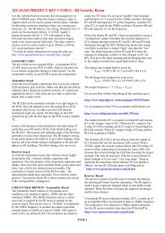
Construction.<br />
Follow the printed circuit overlay with<br />
reference to the circuit diagram where<br />
necessary. Add the lowest height components<br />
to the board first, starting with the resistors. Be<br />
careful to get the electrolytic capacitors in the<br />
correct way around and all parts in their correct<br />
positions. Be careful when soldering the IC not<br />
to use excessive heat. Use some heat sink<br />
compound between the heat sink & the IC.<br />
Also note if you intend to drive it very hard, it<br />
may require a bigger heatsink. The supplied<br />
heatsink is quite adequate for normal use. No<br />
damage will result, but the thermal protection<br />
circuit may limit the power output. Use<br />
shielded signal wire for the input connections,<br />
and at least 16/0.2 hook up wire for DC input<br />
and speaker outputs. Try to keep lead lengths<br />
as short as possible.<br />
It is recommended that you place a solder lug<br />
(supplied) between the heatsink bolt head and<br />
front of the IC mounting tab. (NOT between<br />
the IC and heatsink) Connect the power supply<br />
earth to this lug. This reduces earth currents on<br />
the PC board, and lowers the distortion figures<br />
by a worthwhile amount. The circuit will,<br />
however, perform adequately without it.<br />
Operation.<br />
The circuit is straight forward. Most of the<br />
circuitry is contained within the amplifier<br />
module. C1 & C2 are input coupling capacitors<br />
and block DC, as do C<strong>10</strong> & C11 which are the<br />
output coupling capacitors, and C7 & C9 which<br />
block DC from the feed back loop to the<br />
differential inputs. R3/R5 (and R4/R6) set the<br />
level of feed back. C<strong>10</strong>/R7 (and C11/R8)<br />
provide a high frequency load for stability<br />
where loudspeaker inductive reactance may<br />
become excessive. C4 and C5 provide power<br />
supply decoupling or filtering.<br />
The gain is equal to 1 + (R3/R5) = 37, or 31dB,<br />
minus any input attenuation. The gain may be<br />
increased by reducing the feedback resistors R5<br />
and R6. A value of 22 ohms would provide a<br />
gain of approximately 35 dB. If you need much<br />
more than 40 dB gain, it would be better to use<br />
a preamplifier.<br />
The maximum supply voltage for this Kit is<br />
18V. Check the power supply voltage and<br />
polarity before connecting to the board. We<br />
found no trouble in getting this kit to work. If<br />
yours does not work, first check all external<br />
wiring, make sure there are no shorts, then<br />
check all the component positions and<br />
orientation. Also check all solder joints and<br />
make sure there are no dry joints or solder<br />
bridges.<br />
You may download the full data sheet for the<br />
TDA2005 from my website :<br />
www.quasarelectronics.com/software.htm<br />
Page 1 of 3
6 – <strong>10</strong> <strong>Watt</strong> <strong>Stereo</strong> <strong>Audio</strong> <strong>Amplifier</strong> (<strong>Code</strong> <strong>3143</strong>)<br />
Specifications :<br />
D.C. Input : 8 – 18V at 1 – 2 A<br />
(15 - 30 VA minimum)<br />
Power output : > 8 W RMS / channel, 2 ohm<br />
load, 16V DC supply.<br />
> 6W RMS / channel, 4 ohm<br />
load, 16V DC supply.<br />
> 4W RMS / channel, 4 ohm<br />
load 12V DC supply.<br />
THD<br />
< 0.1% @ 1W, 4ohms.<br />
S/N ratio : > 80 dBA.<br />
Frequency response : ~ 15 Hz to 50 kHz, –3 dB<br />
Gain :<br />
~ 30 dB maximum.<br />
Input level : ~ 150 mV for full output<br />
Components<br />
Resistors :<br />
Total<br />
1 ohm, brown black gold R7, R8 2<br />
33 ohm, orange orange black R5, R6 2<br />
1k ohm, brown black red R1, R9 2<br />
1k2 ohm, brown red red R3, R4 2<br />
120k ohm, brown red yellow R2 1<br />
Capacitors :<br />
2u2 50V C1 C2 2<br />
<strong>10</strong>uF 25V C3 1<br />
<strong>10</strong>0uF 25V C5, C6, C8 3<br />
220uF 25V C7, C9 2<br />
2200uF 16V C12, C13 2<br />
<strong>10</strong>0 nF monoblock C4 1<br />
<strong>10</strong>0 nF mylar C<strong>10</strong>, C11 2<br />
Kit <strong>3143</strong> Printed Circuit Board 1<br />
TDA2005 amplifier module 1<br />
Heat sink, HS215 1<br />
Nut & bolt set for HS 1<br />
<strong>10</strong> k ohm dual gang log pot 1<br />
3 pole terminal block 2<br />
Solder lug 1<br />
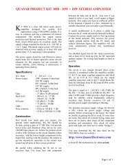
Harmonic Distortion @ 1W RMS Output, 4 ohm load<br />
1 kHz input and 15V DC supply<br />
Page 2 of 3
6 – <strong>10</strong> <strong>Watt</strong> <strong>Stereo</strong> <strong>Audio</strong> <strong>Amplifier</strong> (<strong>Code</strong> <strong>3143</strong>)<br />
Circuit Diagram<br />
Input 1<br />
Input 2<br />
R1<br />
1k<br />
R2<br />
1k<br />
Pot.<br />
1a<br />
Pot.<br />
1b<br />
+<br />
C3<br />
<strong>10</strong>uF<br />
C1<br />
2u2<br />
+<br />
C2<br />
2u2<br />
+<br />
1<br />
5<br />
3<br />
R2<br />
120K<br />
+<br />
-<br />
TDA 2005<br />
+<br />
-<br />
6<br />
9<br />
11<br />
<strong>10</strong><br />
2<br />
7<br />
8<br />
4<br />
+<br />
C4<br />
<strong>10</strong>0 nF<br />
<strong>10</strong>0 uF<br />
C7<br />
+<br />
220 uF<br />
+<br />
<strong>10</strong>0 uF<br />
C9<br />
+<br />
C6<br />
C8<br />
220 uF<br />
R3<br />
1k2<br />
R5<br />
33Ω<br />
R4<br />
1k2<br />
R6<br />
33Ω<br />
+<br />
C5<br />
<strong>10</strong>0 uF 25V<br />
C12<br />
2200 uF<br />
+<br />
C<strong>10</strong> 16V<br />
<strong>10</strong>0 nF<br />
R7<br />
1Ω<br />
C11<br />
<strong>10</strong>0 nF<br />
R8<br />
1Ω<br />
C13<br />
2200 uF<br />
+<br />
16V<br />
+<br />
Vin<br />
8 - 18V<br />
+<br />
+<br />
Gnd<br />
Speaker 1<br />
Speaker 2<br />
Photo showing power supply ground tag mounted on the I.C.<br />
Page 3 of 3