LM3404/04HV 1.0A Constant Current Buck Regulator for Driving ...
LM3404/04HV 1.0A Constant Current Buck Regulator for Driving ... LM3404/04HV 1.0A Constant Current Buck Regulator for Driving ...
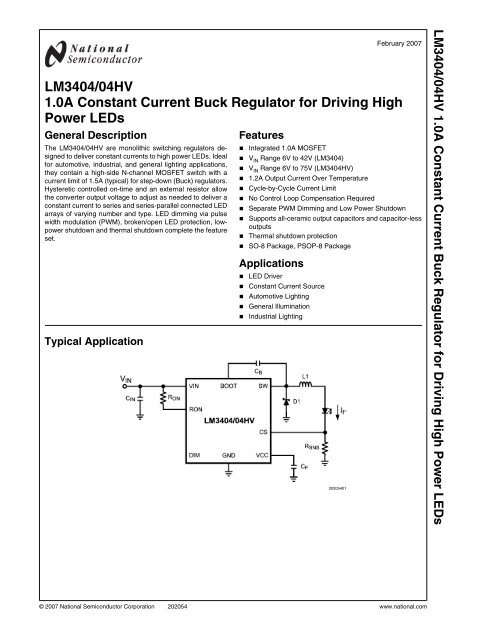
February 2007 LM3404/04HV 1.0A Constant Current Buck Regulator for Driving High Power LEDs General Description The LM3404/04HV are monolithic switching regulators designed to deliver constant currents to high power LEDs. Ideal for automotive, industrial, and general lighting applications, they contain a high-side N-channel MOSFET switch with a current limit of 1.5A (typical) for step-down (Buck) regulators. Hysteretic controlled on-time and an external resistor allow the converter output voltage to adjust as needed to deliver a constant current to series and series-parallel connected LED arrays of varying number and type. LED dimming via pulse width modulation (PWM), broken/open LED protection, lowpower shutdown and thermal shutdown complete the feature set. Typical Application Features ■ Integrated 1.0A MOSFET ■ V IN Range 6V to 42V (LM3404) ■ V IN Range 6V to 75V (LM3404HV) ■ 1.2A Output Current Over Temperature ■ Cycle-by-Cycle Current Limit ■ No Control Loop Compensation Required ■ Separate PWM Dimming and Low Power Shutdown ■ Supports all-ceramic output capacitors and capacitor-less outputs ■ Thermal shutdown protection ■ SO-8 Package, PSOP-8 Package Applications ■ LED Driver ■ Constant Current Source ■ Automotive Lighting ■ General Illumination ■ Industrial Lighting 20205401 LM3404/04HV 1.0A Constant Current Buck Regulator for Driving High Power LEDs © 2007 National Semiconductor Corporation 202054 www.national.com
- Page 2 and 3: LM3404/LM3404HV Connection Diagrams
- Page 4 and 5: LM3404/LM3404HV Absolute Maximum Ra
- Page 6 and 7: LM3404/LM3404HV Symbol Parameter Co
- Page 8 and 9: LM3404/LM3404HV T ON vs V IN , R ON
- Page 10 and 11: LM3404/LM3404HV Block Diagram 20205
- Page 12 and 13: LM3404/LM3404HV V SNS exceeds 300 m
- Page 14 and 15: LM3404/LM3404HV Small values of C O
- Page 16 and 17: LM3404/LM3404HV at a typical peak c
- Page 18 and 19: LM3404/LM3404HV With the target rip
- Page 20 and 21: LM3404/LM3404HV 20205428 FIGURE 7.
- Page 22 and 23: LM3404/LM3404HV Physical Dimensions
- Page 24: LM3404/04HV 1.0A Constant Current B
February 2007<br />
<strong>LM3404</strong>/<strong>04HV</strong><br />
<strong>1.0A</strong> <strong>Constant</strong> <strong>Current</strong> <strong>Buck</strong> <strong>Regulator</strong> <strong>for</strong> <strong>Driving</strong> High<br />
Power LEDs<br />
General Description<br />
The <strong>LM3404</strong>/<strong>04HV</strong> are monolithic switching regulators designed<br />
to deliver constant currents to high power LEDs. Ideal<br />
<strong>for</strong> automotive, industrial, and general lighting applications,<br />
they contain a high-side N-channel MOSFET switch with a<br />
current limit of 1.5A (typical) <strong>for</strong> step-down (<strong>Buck</strong>) regulators.<br />
Hysteretic controlled on-time and an external resistor allow<br />
the converter output voltage to adjust as needed to deliver a<br />
constant current to series and series-parallel connected LED<br />
arrays of varying number and type. LED dimming via pulse<br />
width modulation (PWM), broken/open LED protection, lowpower<br />
shutdown and thermal shutdown complete the feature<br />
set.<br />
Typical Application<br />
Features<br />
■ Integrated <strong>1.0A</strong> MOSFET<br />
■ V IN Range 6V to 42V (<strong>LM3404</strong>)<br />
■ V IN Range 6V to 75V (<strong>LM3404</strong>HV)<br />
■ 1.2A Output <strong>Current</strong> Over Temperature<br />
■ Cycle-by-Cycle <strong>Current</strong> Limit<br />
■ No Control Loop Compensation Required<br />
■ Separate PWM Dimming and Low Power Shutdown<br />
■ Supports all-ceramic output capacitors and capacitor-less<br />
outputs<br />
■ Thermal shutdown protection<br />
■ SO-8 Package, PSOP-8 Package<br />
Applications<br />
■ LED Driver<br />
■ <strong>Constant</strong> <strong>Current</strong> Source<br />
■ Automotive Lighting<br />
■ General Illumination<br />
■ Industrial Lighting<br />
20205401<br />
<strong>LM3404</strong>/<strong>04HV</strong> <strong>1.0A</strong> <strong>Constant</strong> <strong>Current</strong> <strong>Buck</strong> <strong>Regulator</strong> <strong>for</strong> <strong>Driving</strong> High Power LEDs<br />
© 2007 National Semiconductor Corporation 202054 www.national.com
<strong>LM3404</strong>/<strong>LM3404</strong>HV<br />
Connection Diagrams<br />
20205402<br />
8-Lead Plastic SO-8 Package<br />
NS Package Number M08A<br />
20205456<br />
8-Lead Plastic PSOP-8 Package<br />
NS Package Number MRA08B<br />
Ordering In<strong>for</strong>mation<br />
Order Number Package Type NSC Package Drawing Supplied As<br />
<strong>LM3404</strong>MA<br />
<strong>LM3404</strong>MAX<br />
<strong>LM3404</strong>HVMA<br />
<strong>LM3404</strong>HVMAX<br />
<strong>LM3404</strong>MR<br />
<strong>LM3404</strong>MRX<br />
<strong>LM3404</strong>HVMR<br />
<strong>LM3404</strong>HVMRX<br />
Pin Descriptions<br />
SO-8<br />
PSOP-8<br />
M08A<br />
MRA08B<br />
Pin(s) Name Description Application In<strong>for</strong>mation<br />
95 units in anti-static rails<br />
2500 units on tape and reel<br />
95 units in anti-static rails<br />
2500 units on tape and reel<br />
95 units in anti-static rails<br />
2500 units on tape and reel<br />
95 units in anti-static rails<br />
2500 units on tape and reel<br />
1 SW Switch pin Connect this pin to the output inductor and Schottky diode.<br />
2 BOOT MOSFET drive bootstrap pin Connect a 10 nF ceramic capacitor from this pin to SW.<br />
3 DIM Input <strong>for</strong> PWM dimming Connect a logic-level PWM signal to this pin to enable/disable the<br />
power MOSFET and reduce the average light output of the LED array.<br />
4 GND Ground pin Connect this pin to system ground.<br />
5 CS <strong>Current</strong> sense feedback pin Set the current through the LED array by connecting a resistor from<br />
this pin to ground.<br />
6 RON On-time control pin A resistor connected from this pin to VIN sets the regulator controlled<br />
on-time.<br />
7 VCC Output of the internal 7V linear<br />
regulator<br />
Bypass this pin to ground with a minimum 0.1 µF ceramic capacitor<br />
with X5R or X7R dielectric.<br />
8 VIN Input voltage pin Nominal operating input range <strong>for</strong> this pin is 6V to 42V (<strong>LM3404</strong>) or 6V<br />
to 75V (<strong>LM3404</strong>HV).<br />
DAP GND Thermal Pad Connect to ground. Place 4-6 vias from DAP to bottom layer ground<br />
plane.<br />
www.national.com 2
Absolute Maximum Ratings<br />
(<strong>LM3404</strong>) (Note 1)<br />
If Military/Aerospace specified devices are required,<br />
please contact the National Semiconductor Sales Office/<br />
Distributors <strong>for</strong> availability and specifications.<br />
VIN to GND<br />
-0.3V to 45V<br />
BOOT to GND<br />
-0.3V to 59V<br />
SW to GND<br />
-1.5V to 45V<br />
BOOT to VCC<br />
-0.3V to 45V<br />
BOOT to SW<br />
-0.3V to 14V<br />
VCC to GND<br />
-0.3V to 14V<br />
DIM to GND<br />
-0.3V to 7V<br />
CS to GND<br />
-0.3V to 7V<br />
RON to GND<br />
-0.3V to 7V<br />
Junction Temperature 150°C<br />
Storage Temp. Range -65°C to 125°C<br />
ESD Rating (Note 2)<br />
2kV<br />
Soldering In<strong>for</strong>mation<br />
Lead Temperature (Soldering,<br />
10sec) 260°C<br />
Infrared/Convection Reflow (15sec) 235°C<br />
Operating Ratings (<strong>LM3404</strong>)<br />
(Note 1)<br />
V IN<br />
Junction Temperature Range<br />
Thermal Resistance θ JA<br />
(SO-8 Package)<br />
Thermal Resistance θ JA<br />
(PSOP-8 Package) (Note 5)<br />
6V to 42V<br />
−40°C to +125°C<br />
155°C/W<br />
50°C/W<br />
<strong>LM3404</strong>/<strong>LM3404</strong>HV<br />
3 www.national.com
<strong>LM3404</strong>/<strong>LM3404</strong>HV<br />
Absolute Maximum Ratings<br />
(<strong>LM3404</strong>HV) (Note 1)<br />
If Military/Aerospace specified devices are required,<br />
please contact the National Semiconductor Sales Office/<br />
Distributors <strong>for</strong> availability and specifications.<br />
VIN to GND<br />
-0.3V to 76V<br />
BOOT to GND<br />
-0.3V to 90V<br />
SW to GND<br />
-1.5V to 76V<br />
BOOT to VCC<br />
-0.3V to 76V<br />
BOOT to SW<br />
-0.3V to 14V<br />
VCC to GND<br />
-0.3V to 14V<br />
DIM to GND<br />
-0.3V to 7V<br />
CS to GND<br />
-0.3V to 7V<br />
RON to GND<br />
-0.3V to 7V<br />
Junction Temperature 150°C<br />
Storage Temp. Range -65°C to 125°C<br />
ESD Rating (Note 2)<br />
2kV<br />
Soldering In<strong>for</strong>mation<br />
Lead Temperature (Soldering,<br />
10sec) 260°C<br />
Infrared/Convection Reflow (15sec) 235°C<br />
Operating Ratings (<strong>LM3404</strong>HV)<br />
(Note 1)<br />
V IN<br />
Junction Temperature Range<br />
Thermal Resistance θ JA<br />
(SO-8 Package)<br />
Thermal Resistance θ JA<br />
(PSOP-8 Package) (Note 5)<br />
6V to 75V<br />
−40°C to +125°C<br />
155°C/W<br />
50°C/W<br />
www.national.com 4
Electrical Characteristics V IN = 24V unless otherwise indicated. Typicals and limits appearing in plain type apply<br />
<strong>for</strong> T A = T J = +25°C. (Note 4) Limits appearing in boldface type apply over full Operating Temperature Range. Datasheet min/<br />
max specification limits are guaranteed by design, test, or statistical analysis.<br />
<strong>LM3404</strong><br />
Symbol Parameter Conditions Min Typ Max Units<br />
SYSTEM PARAMETERS<br />
t ON-1 On-time 1 V IN = 10V, R ON = 200 kΩ 2.1 2.75 3.4 µs<br />
<strong>LM3404</strong>/<strong>LM3404</strong>HV<br />
t ON-2 On-time 2 V IN = 40V, R ON = 200 kΩ 515 675 835 ns<br />
<strong>LM3404</strong>HV<br />
Symbol Parameter Conditions Min Typ Max Units<br />
SYSTEM PARAMETERS<br />
t ON-1 On-time 1 V IN = 10V, R ON = 200 kΩ 2.1 2.75 3.4 µs<br />
t ON-2 On-time 2 V IN = 70V, R ON = 200 kΩ 325 415 505 ns<br />
<strong>LM3404</strong>/<strong>LM3404</strong>HV<br />
Symbol Parameter Conditions Min Typ Max Units<br />
REGULATION AND OVER-VOLTAGE COMPARATORS<br />
V REF-REG CS Regulation Threshold CS Decreasing, SW turns on 194 200 206 mV<br />
V REF-0V CS Over-voltage Threshold CS Increasing, SW turns off 300 mV<br />
I CS CS Bias <strong>Current</strong> CS = 0V 0.1 µA<br />
SHUTDOWN<br />
V SD-TH Shutdown Threshold R ON / SD Increasing 0.3 0.7 1.05 V<br />
V SD-HYS Shutdown Hysteresis R ON / SD Decreasing 40 mV<br />
OFF TIMER<br />
t OFF-MIN Minimum Off-time CS = 0V 270 ns<br />
INTERNAL REGULATOR<br />
V CC-REG V CC Regulated Output 6.4 7 7.4 V<br />
V IN-DO V IN - V CC I CC = 5 mA, 6.0V < V IN < 8.0V 300 mV<br />
V CC-BP-TH V CC Bypass Threshold V IN Increasing 8.8 V<br />
V CC-BP-HYS V CC Bypass Hysteresis V IN Decreasing 230 mV<br />
V CC-Z-6<br />
V CC Output Impedance V IN = 6V 55 Ω<br />
V CC-Z-8<br />
(0 mA < I CC < 5 mA)<br />
V IN = 8V 50<br />
V CC-Z-24 V IN = 24V 0.4<br />
V CC-LIM V CC <strong>Current</strong> Limit (Note 3) V IN = 24V, V CC = 0V 16 mA<br />
V CC-UV-TH<br />
V CC-UV-HYS<br />
V CC-UV-DLY<br />
V CC Under-voltage Lock-out<br />
Threshold<br />
V CC Under-voltage Lock-out<br />
Hysteresis<br />
V CC Under-voltage Lock-out<br />
Filter Delay<br />
V CC Increasing 5.3 V<br />
V CC Decreasing 150 mV<br />
100 mV Overdrive 3 µs<br />
I IN-OP I IN Operating <strong>Current</strong> Non-switching, CS = 0.5V 625 900 µA<br />
I IN-SD I IN Shutdown <strong>Current</strong> RON / SD = 0V 95 180 µA<br />
CURRENT LIMIT<br />
I LIM <strong>Current</strong> Limit Threshold 1.2 1.5 1.8 A<br />
5 www.national.com
<strong>LM3404</strong>/<strong>LM3404</strong>HV<br />
Symbol Parameter Conditions Min Typ Max Units<br />
DIM COMPARATOR<br />
V IH Logic High DIM Increasing 2.2 V<br />
V IL Logic Low DIM Decreasing 0.8 V<br />
I DIM-PU DIM Pull-up <strong>Current</strong> DIM = 1.5V 80 µA<br />
MOSFET AND DRIVER<br />
R DS-ON <strong>Buck</strong> Switch On Resistance I SW = 200mA, BST-SW = 6.3V 0.37 0.75 Ω<br />
V DR-UVLO<br />
V DR-HYS<br />
THERMAL SHUTDOWN<br />
BST Under-voltage Lock-out<br />
Threshold<br />
BST Under-voltage Lock-out<br />
Hysteresis<br />
BST–SW Increasing 1.7 3 4 V<br />
BST–SW Decreasing 400 mV<br />
T SD Thermal Shutdown Threshold 165 °C<br />
T SD-HYS Thermal Shutdown Hysteresis 25 °C<br />
THERMAL RESISTANCE<br />
θ JA<br />
Junction to Ambient SOIC-8 Package 155 °C/W<br />
PSOP-8 Package (Note 5) 50<br />
Note 1: Absolute Maximum Ratings indicate limits beyond which damage to the device may occur. Operating Ratings indicate conditions <strong>for</strong> which the device is<br />
intended to be functional, but specific per<strong>for</strong>mance is not guaranteed. For guaranteed specifications and the test conditions, see Electrical Characteristics.<br />
Note 2: The human body model is a 100 pF capacitor discharged through a 1.5 kΩ resistor into each pin.<br />
Note 3: VCC provides self bias <strong>for</strong> the internal gate drive and control circuits. Device thermal limitations limit external loading.<br />
Note 4: Typical specifications represent the most likely parametric norm at 25°C operation.<br />
Note 5: θ JA of 50°C/W with DAP soldered to a minimum of 2 square inches of 1oz. copper on the top or bottom PCB layer.<br />
www.national.com 6
Typical Per<strong>for</strong>mance Characteristics<br />
V REF vs Temperature (V IN = 24V)<br />
V REF vs V IN , <strong>LM3404</strong> (T A = 25°C)<br />
<strong>LM3404</strong>/<strong>LM3404</strong>HV<br />
V REF vs V IN , <strong>LM3404</strong>HV (T A = 25°C)<br />
20205450<br />
20205451<br />
<strong>Current</strong> Limit vs Temperature (V IN = 24V)<br />
20205452<br />
<strong>Current</strong> Limit vs V IN , <strong>LM3404</strong> (T A = 25°C)<br />
20205453<br />
<strong>Current</strong> Limit vs V IN , <strong>LM3404</strong>HV (T A = 25°C)<br />
20205454<br />
20205455<br />
7 www.national.com
<strong>LM3404</strong>/<strong>LM3404</strong>HV<br />
T ON vs V IN ,<br />
R ON = 100 kΩ (T A = 25°C)<br />
T ON vs V IN ,<br />
(T A = 25°C)<br />
20205435<br />
20205436<br />
T ON vs V IN ,<br />
(T A = 25°C)<br />
T ON vs R ON , <strong>LM3404</strong><br />
(T A = 25°C)<br />
20205437<br />
20205444<br />
T ON vs R ON , <strong>LM3404</strong>HV<br />
(T A = 25°C)<br />
V CC vs V IN<br />
(T A = 25°C)<br />
20205438<br />
20205439<br />
www.national.com 8
V O-MAX vs f SW , <strong>LM3404</strong><br />
(T A = 25°C)<br />
V O-MIN vs f SW , <strong>LM3404</strong><br />
(T A = 25°C)<br />
<strong>LM3404</strong>/<strong>LM3404</strong>HV<br />
20205440<br />
20205441<br />
V O-MAX vs f SW , <strong>LM3404</strong>HV<br />
(T A = 25°C)<br />
V O-MIN vs f SW , <strong>LM3404</strong>HV<br />
(T A = 25°C)<br />
20205442<br />
20205443<br />
9 www.national.com
<strong>LM3404</strong>/<strong>LM3404</strong>HV<br />
Block Diagram<br />
20205403<br />
Application In<strong>for</strong>mation<br />
THEORY OF OPERATION<br />
The <strong>LM3404</strong> and <strong>LM3404</strong>HV are buck regulators with a wide<br />
input voltage range, low voltage reference, and a fast output<br />
enable/disable function. These features combine to make<br />
them ideal <strong>for</strong> use as a constant current source <strong>for</strong> LEDs with<br />
<strong>for</strong>ward currents as high as 1.2A. The controlled on-time<br />
(COT) architecture is a combination of hysteretic mode control<br />
and a one-shot on-timer that varies inversely with input<br />
voltage. Hysteretic operation eliminates the need <strong>for</strong> smallsignal<br />
control loop compensation. When the converter runs in<br />
continuous conduction mode (CCM) the controlled on-time<br />
maintains a constant switching frequency over the range of<br />
input voltage. Fast transient response, PWM dimming, a low<br />
power shutdown mode, and simple output overvoltage protection<br />
round out the functions of the <strong>LM3404</strong>/<strong>04HV</strong>.<br />
CONTROLLED ON-TIME OVERVIEW<br />
Figure 1 shows the feedback system used to control the current<br />
through an array of LEDs. A voltage signal, V SNS , is<br />
created as the LED current flows through the current setting<br />
resistor, R SNS , to ground. V SNS is fed back to the CS pin,<br />
where it is compared against a 200 mV reference, V REF . The<br />
on-comparator turns on the power MOSFET when V SNS falls<br />
below V REF . The power MOSFET conducts <strong>for</strong> a controlled<br />
on-time, t ON , set by an external resistor, R ON , and by the input<br />
voltage, V IN . On-time is governed by the following equation:<br />
At the conclusion of t ON the power MOSFET turns off <strong>for</strong> a<br />
minimum off-time, t OFF-MIN , of 300 ns. Once t OFF-MIN is complete<br />
the CS comparator compares V SNS and V REF again,<br />
waiting to begin the next cycle.<br />
20205405<br />
FIGURE 1. Comparator and One-Shot<br />
The <strong>LM3404</strong>/<strong>04HV</strong> regulators should be operated in continuous<br />
conduction mode (CCM), where inductor current stays<br />
positive throughout the switching cycle. During steady-state<br />
www.national.com 10
CCM operation, the converter maintains a constant switching<br />
frequency that can be selected using the following equation:<br />
V F = <strong>for</strong>ward voltage of each LED, n = number of LEDs in<br />
series<br />
AVERAGE LED CURRENT ACCURACY<br />
The COT architecture regulates the valley of ΔV SNS , the AC<br />
portion of V SNS . To determine the average LED current (which<br />
is also the average inductor current) the valley inductor current<br />
is calculated using the following expression:<br />
In this equation t SNS represents the propagation delay of the<br />
CS comparator, and is approximately 220 ns. The average<br />
inductor/LED current is equal to I L-MIN plus one-half of the inductor<br />
current ripple, Δi L :<br />
I F = I L = I L-MIN + Δi L / 2<br />
Detailed in<strong>for</strong>mation <strong>for</strong> the calculation of Δi L is given in the<br />
Design Considerations section.<br />
MAXIMUM OUTPUT VOLTAGE<br />
The 300 ns minimum off-time limits the maximum duty cycle<br />
of the converter, D MAX , and in turn the maximum output voltage,<br />
V O(MAX) , determined by the following equations:<br />
The maximum number of LEDs, n MAX , that can be placed in<br />
a single series string is governed by V O(MAX) and the maximum<br />
<strong>for</strong>ward voltage of the LEDs used, V F(MAX) , using the<br />
expression:<br />
At low switching frequency the maximum duty cycle and output<br />
voltage are higher, allowing the <strong>LM3404</strong>/<strong>04HV</strong> to regulate<br />
output voltages that are nearly equal to input voltage. The<br />
following equation relates switching frequency to maximum<br />
output voltage, and is also shown graphically in the Typical<br />
Per<strong>for</strong>mance Characteristics section:<br />
MINIMUM OUTPUT VOLTAGE<br />
The minimum recommended on-time <strong>for</strong> the <strong>LM3404</strong>/<strong>04HV</strong> is<br />
300 ns. This lower limit <strong>for</strong> t ON determines the minimum duty<br />
cycle and output voltage that can be regulated based on input<br />
voltage and switching frequency. The relationship is determined<br />
by the following equation, shown on the same graphs<br />
as maximum output voltage in the Typical Per<strong>for</strong>mance Characteristics<br />
section:<br />
HIGH VOLTAGE BIAS REGULATOR<br />
The <strong>LM3404</strong>/<strong>04HV</strong> contains an internal linear regulator with<br />
a 7V output, connected between the VIN and the VCC pins.<br />
The VCC pin should be bypassed to the GND pin with a 0.1<br />
µF ceramic capacitor connected as close as possible to the<br />
pins of the IC. VCC tracks VIN until VIN reaches 8.8V (typical)<br />
and then regulates at 7V as VIN increases. Operation begins<br />
when VCC crosses 5.25V.<br />
INTERNAL MOSFET AND DRIVER<br />
The <strong>LM3404</strong>/<strong>04HV</strong> features an internal power MOSFET as<br />
well as a floating driver connected from the SW pin to the<br />
BOOT pin. Both rise time and fall time are 20 ns each (typical)<br />
and the approximate gate charge is 6 nC. The high-side rail<br />
<strong>for</strong> the driver circuitry uses a bootstrap circuit consisting of an<br />
internal high-voltage diode and an external 10 nF capacitor,<br />
C B . V CC charges C B through the internal diode while the power<br />
MOSFET is off. When the MOSFET turns on, the internal<br />
diode reverse biases. This creates a floating supply equal to<br />
the V CC voltage minus the diode drop to drive the MOSFET<br />
when its source voltage is equal to V IN .<br />
FAST SHUTDOWN FOR PWM DIMMING<br />
The DIM pin of the <strong>LM3404</strong>/<strong>04HV</strong> is a TTL compatible input<br />
<strong>for</strong> low frequency PWM dimming of the LED. A logic low (below<br />
0.8V) at DIM will disable the internal MOSFET and shut<br />
off the current flow to the LED array. While the DIM pin is in<br />
a logic low state the support circuitry (driver, bandgap, VCC)<br />
remains active in order to minimize the time needed to turn<br />
the LED array back on when the DIM pin sees a logic high<br />
(above 2.2V). A 75 µA (typical) pull-up current ensures that<br />
the <strong>LM3404</strong>/<strong>04HV</strong> is on when DIM pin is open circuited, eliminating<br />
the need <strong>for</strong> a pull-up resistor. Dimming frequency,<br />
f DIM , and duty cycle, D DIM , are limited by the LED current rise<br />
time and fall time and the delay from activation of the DIM pin<br />
to the response of the internal power MOSFET. In general,<br />
f DIM should be at least one order of magnitude lower than the<br />
steady state switching frequency in order to prevent aliasing.<br />
PEAK CURRENT LIMIT<br />
The current limit comparator of the <strong>LM3404</strong>/<strong>04HV</strong> will engage<br />
whenever the power MOSFET current (equal to the inductor<br />
current while the MOSFET is on) exceeds 1.5A (typical). The<br />
power MOSFET is disabled <strong>for</strong> a cool-down time that is approximately<br />
75x the steady-state on-time. At the conclusion<br />
of this cool-down time the system re-starts. If the current limit<br />
condition persists the cycle of cool-down time and restarting<br />
will continue, creating a low-power hiccup mode, minimizing<br />
thermal stress on the <strong>LM3404</strong>/<strong>04HV</strong> and the external circuit<br />
components.<br />
OVER-VOLTAGE/OVER-CURRENT COMPARATOR<br />
The CS pin includes an output over-voltage/over-current<br />
comparator that will disable the power MOSFET whenever<br />
<strong>LM3404</strong>/<strong>LM3404</strong>HV<br />
11 www.national.com
<strong>LM3404</strong>/<strong>LM3404</strong>HV<br />
V SNS exceeds 300 mV. This threshold provides a hard limit<br />
<strong>for</strong> the output current. Output current overshoot is limited to<br />
300 mV / R SNS by this comparator during transients.<br />
The OVP/OCP comparator can also be used to prevent the<br />
output voltage from rising to V O(MAX) in the event of an output<br />
open-circuit. This is the most common failure mode <strong>for</strong> LEDs,<br />
due to breaking of the bond wires. In a current regulator an<br />
output open circuit causes V SNS to fall to zero, commanding<br />
maximum duty cycle. Figure 2 shows a method using a zener<br />
diode, Z1, and zener limiting resistor, R Z , to limit output voltage<br />
to the reverse breakdown voltage of Z1 plus 200 mV. The<br />
zener diode reverse breakdown voltage, V Z , must be greater<br />
than the maximum combined V F of all LEDs in the array. The<br />
maximum recommended value <strong>for</strong> R Z is 1 kΩ.<br />
As discussed in the Maximum Output Voltage section, there<br />
is a limit to how high V O can rise during an output open-circuit<br />
that is always less than V IN . If no output capacitor is used, the<br />
output stage of the <strong>LM3404</strong>/<strong>04HV</strong> is capable of withstanding<br />
V O(MAX) indefinitely, however the voltage at the output end of<br />
the inductor will oscillate and can go above V IN or below 0V.<br />
A small (typically 10 nF) capacitor across the LED array<br />
dampens this oscillation. For circuits that use an output capacitor,<br />
the system can still withstand V O(MAX) indefinitely as<br />
long as C O is rated to handle V IN . The high current paths are<br />
blocked in output open-circuit and the risk of thermal stress is<br />
minimal, hence the user may opt to allow the output voltage<br />
to rise in the case of an open-circuit LED failure.<br />
20205412<br />
FIGURE 2. Output Open Circuit Protection<br />
LOW POWER SHUTDOWN<br />
The <strong>LM3404</strong>/<strong>04HV</strong> can be placed into a low power state (I IN-<br />
SD = 90 µA) by grounding the RON pin with a signal-level<br />
MOSFET as shown in Figure 3. Low power MOSFETs like the<br />
2N7000, 2N3904, or equivalent are recommended devices<br />
<strong>for</strong> putting the <strong>LM3404</strong>/<strong>04HV</strong> into low power shutdown. Logic<br />
gates can also be used to shut down the <strong>LM3404</strong>/<strong>04HV</strong> as<br />
long as the logic low voltage is below the over temperature<br />
minimum threshold of 0.3V. Noise filter circuitry on the RON<br />
pin can cause a few pulses with longer on-times than normal<br />
after RON is grounded or released. In these cases the OVP/<br />
OCP comparator will ensure that the peak inductor or LED<br />
current does not exceed 300 mV / R SNS .<br />
20205413<br />
FIGURE 3. Low Power Shutdown<br />
www.national.com 12
THERMAL SHUTDOWN<br />
Internal thermal shutdown circuitry is provided to protect the<br />
IC in the event that the maximum junction temperature is exceeded.<br />
The threshold <strong>for</strong> thermal shutdown is 165°C with a<br />
25°C hysteresis (both values typical). During thermal shutdown<br />
the MOSFET and driver are disabled.<br />
Design Considerations<br />
SWITCHING FREQUENCY<br />
Switching frequency is selected based on the trade-offs between<br />
efficiency (better at low frequency), solution size/cost<br />
(smaller at high frequency), and the range of output voltage<br />
that can be regulated (wider at lower frequency.) Many applications<br />
place limits on switching frequency due to EMI sensitivity.<br />
The on-time of the <strong>LM3404</strong>/<strong>04HV</strong> can be programmed<br />
<strong>for</strong> switching frequencies ranging from the 10’s of kHz to over<br />
1 MHz. The maximum switching frequency is limited only by<br />
the minimum on-time and minimum off-time requirements.<br />
LED RIPPLE CURRENT<br />
Selection of the ripple current, Δi F , through the LED array is<br />
analogous to the selection of output ripple voltage in a standard<br />
voltage regulator. Where the output ripple in a voltage<br />
regulator is commonly ±1% to ±5% of the DC output voltage,<br />
LED manufacturers generally recommend values <strong>for</strong> Δi F<br />
ranging from ±5% to ±20% of I F . Higher LED ripple current<br />
allows the use of smaller inductors, smaller output capacitors,<br />
or no output capacitors at all. The advantages of higher ripple<br />
current are reduction in the solution size and cost. Lower ripple<br />
current requires more output inductance, higher switching<br />
frequency, or additional output capacitance. The advantages<br />
of lower ripple current are a reduction in heating in the LED<br />
itself and greater tolerance in the average LED current be<strong>for</strong>e<br />
the current limit of the LED or the driving circuitry is reached.<br />
BUCK CONVERTERS WITHOUT OUTPUT CAPACITORS<br />
The buck converter is unique among non-isolated topologies<br />
because of the direct connection of the inductor to the load<br />
during the entire switching cycle. By definition an inductor will<br />
control the rate of change of current that flows through it, and<br />
this control over current ripple <strong>for</strong>ms the basis <strong>for</strong> component<br />
selection in both voltage regulators and current regulators. A<br />
current regulator such as the LED driver <strong>for</strong> which the<br />
<strong>LM3404</strong>/<strong>04HV</strong> was designed focuses on the control of the<br />
current through the load, not the voltage across it. A constant<br />
current regulator is free of load current transients, and has no<br />
need of output capacitance to supply the load and maintain<br />
output voltage. Referring to the Typical Application circuit on<br />
the front page of this datasheet, the inductor and LED can<br />
<strong>for</strong>m a single series chain, sharing the same current. When<br />
no output capacitor is used, the same equations that govern<br />
inductor ripple current, Δi L , also apply to the LED ripple current,<br />
Δi F . For a controlled on-time converter such as<br />
<strong>LM3404</strong>/<strong>04HV</strong> the ripple current is described by the following<br />
expression:<br />
BUCK CONVERTERS WITH OUTPUT CAPACITORS<br />
A capacitor placed in parallel with the LED or array of LEDs<br />
can be used to reduce the LED current ripple while keeping<br />
the same average current through both the inductor and the<br />
LED array. This technique is demonstrated in Design Examples<br />
1 and 2. With this topology the output inductance can be<br />
lowered, making the magnetics smaller and less expensive.<br />
Alternatively, the circuit could be run at lower frequency but<br />
keep the same inductor value, improving the efficiency and<br />
expanding the range of output voltage that can be regulated.<br />
Both the peak current limit and the OVP/OCP comparator still<br />
monitor peak inductor current, placing a limit on how large<br />
Δi L can be even if Δi F is made very small. A parallel output<br />
capacitor is also useful in applications where the inductor or<br />
input voltage tolerance is poor. Adding a capacitor that reduces<br />
Δi F to well below the target provides headroom <strong>for</strong><br />
changes in inductance or V IN that might otherwise push the<br />
peak LED ripple current too high.<br />
Figure 4 shows the equivalent impedances presented to the<br />
inductor current ripple when an output capacitor, C O , and its<br />
equivalent series resistance (ESR) are placed in parallel with<br />
the LED array. The entire inductor ripple current flows through<br />
R SNS to provide the required 25 mV of ripple voltage <strong>for</strong> proper<br />
operation of the CS comparator.<br />
20205415<br />
FIGURE 4. LED and C O Ripple <strong>Current</strong><br />
To calculate the respective ripple currents the LED array is<br />
represented as a dynamic resistance, r D . LED dynamic resistance<br />
is not always specified on the manufacturer’s<br />
datasheet, but it can be calculated as the inverse slope of the<br />
LED’s V F vs. I F curve. Note that dividing V F by I F will give an<br />
incorrect value that is 5x to 10x too high. Total dynamic resistance<br />
<strong>for</strong> a string of n LEDs connected in series can be<br />
calculated as the r D of one device multiplied by n. Inductor<br />
ripple current is still calculated with the expression from <strong>Buck</strong><br />
<strong>Regulator</strong>s without Output Capacitors. The following equations<br />
can then be used to estimate Δi F when using a parallel<br />
capacitor:<br />
<strong>LM3404</strong>/<strong>LM3404</strong>HV<br />
A minimum ripple voltage of 25 mV is recommended at the<br />
CS pin to provide good signal to noise ratio (SNR). The CS<br />
pin ripple voltage, Δv SNS , is described by the following:<br />
Δv SNS = Δi F x R SNS<br />
The calculation <strong>for</strong> Z C assumes that the shape of the inductor<br />
ripple current is approximately sinusoidal.<br />
13 www.national.com
<strong>LM3404</strong>/<strong>LM3404</strong>HV<br />
Small values of C O that do not significantly reduce Δi F can<br />
also be used to control EMI generated by the switching action<br />
of the <strong>LM3404</strong>/<strong>04HV</strong>. EMI reduction becomes more important<br />
as the length of the connections between the LED and the<br />
rest of the circuit increase.<br />
INPUT CAPACITORS<br />
Input capacitors at the VIN pin of the <strong>LM3404</strong>/<strong>04HV</strong> are selected<br />
using requirements <strong>for</strong> minimum capacitance and rms<br />
ripple current. The input capacitors supply pulses of current<br />
approximately equal to I F while the power MOSFET is on, and<br />
are charged up by the input voltage while the power MOSFET<br />
is off. Switching converters such as the <strong>LM3404</strong>/<strong>04HV</strong> have<br />
a negative input impedance due to the decrease in input current<br />
as input voltage increases. This inverse proportionality of<br />
input current to input voltage can cause oscillations (sometimes<br />
called ‘power supply interaction’) if the magnitude of the<br />
negative input impedance is greater the the input filter<br />
impedance. Minimum capacitance can be selected by comparing<br />
the input impedance to the converter’s negative resistance;<br />
however this requires accurate calculation of the input<br />
voltage source inductance and resistance, quantities which<br />
can be difficult to determine. An alternative method to select<br />
the minimum input capacitance, C IN(MIN) , is to select the maximum<br />
input voltage ripple which can be tolerated. This value,<br />
Δv IN(MAX) , is equal to the change in voltage across C IN during<br />
the converter on-time, when C IN supplies the load current.<br />
C IN(MIN) can be selected with the following:<br />
A good starting point <strong>for</strong> selection of C IN is to use an input<br />
voltage ripple of 5% to 10% of V IN . A minimum input capacitance<br />
of 2x the C IN(MIN) value is recommended <strong>for</strong> all<br />
<strong>LM3404</strong>/<strong>04HV</strong> circuits. To determine the rms current rating,<br />
the following <strong>for</strong>mula can be used:<br />
Ceramic capacitors are the best choice <strong>for</strong> the input to the<br />
<strong>LM3404</strong>/<strong>04HV</strong> due to their high ripple current rating, low ESR,<br />
low cost, and small size compared to other types. When selecting<br />
a ceramic capacitor, special attention must be paid to<br />
the operating conditions of the application. Ceramic capacitors<br />
can lose one-half or more of their capacitance at their<br />
rated DC voltage bias and also lose capacitance with extremes<br />
in temperature. A DC voltage rating equal to twice the<br />
expected maximum input voltage is recommended. In addition,<br />
the minimum quality dielectric which is suitable <strong>for</strong><br />
switching power supply inputs is X5R, while X7R or better is<br />
preferred.<br />
RECIRCULATING DIODE<br />
The <strong>LM3404</strong>/<strong>04HV</strong> is a non-synchronous buck regulator that<br />
requires a recirculating diode D1 (see the Typical Application<br />
circuit) to carrying the inductor current during the MOSFET<br />
off-time. The most efficient choice <strong>for</strong> D1 is a Schottky diode<br />
due to low <strong>for</strong>ward drop and near-zero reverse recovery time.<br />
D1 must be rated to handle the maximum input voltage plus<br />
any switching node ringing when the MOSFET is on. In practice<br />
all switching converters have some ringing at the switching<br />
node due to the diode parasitic capacitance and the lead<br />
inductance. D1 must also be rated to handle the average current,<br />
I D , calculated as:<br />
I D = (1 – D) x I F<br />
This calculation should be done at the maximum expected<br />
input voltage. The overall converter efficiency becomes more<br />
dependent on the selection of D1 at low duty cycles, where<br />
the recirculating diode carries the load current <strong>for</strong> an increasing<br />
percentage of the time. This power dissipation can be<br />
calculating by checking the typical diode <strong>for</strong>ward voltage,<br />
V D , from the I-V curve on the product datasheet and then<br />
multiplying it by I D . Diode datasheets will also provide a typical<br />
junction-to-ambient thermal resistance, θ JA , which can be<br />
used to estimate the operating die temperature of the device.<br />
Multiplying the power dissipation (P D = I D x V D ) by θ JA gives<br />
the temperature rise. The diode case size can then be selected<br />
to maintain the Schottky diode temperature below the<br />
operational maximum.<br />
Design Example 1: <strong>LM3404</strong><br />
The first example circuit will guide the user through component<br />
selection <strong>for</strong> an architectural accent lighting application.<br />
A regulated DC voltage input of 24V ±10% will power a 5.4W<br />
"warm white" LED module that consists of four LEDs in a 2 x<br />
2 series-parallel configuration. The module will be treated as<br />
a two-terminal element and driven with a <strong>for</strong>ward current of<br />
700 mA ±5%. The typical <strong>for</strong>ward voltage of the LED module<br />
in thermal steady state is 6.9V, hence the average output<br />
voltage will be 7.1V. The objective of this application is to<br />
place the complete current regulator and LED module in a<br />
compact space <strong>for</strong>merly occupied by a halogen light source.<br />
(The LED will be on a separate metal-core PCB and heatsink.)<br />
Switching frequency will be 400 kHz to keep switching loss<br />
low, as the confined space with no air-flow requires a maximum<br />
temperature rise of 50°C in each circuit component. A<br />
small solution size is also important, as the regulator must fit<br />
on a circular PCB with a 1.5" diameter. A complete bill of materials<br />
can be found in Table 1 at the end of this datasheet.<br />
www.national.com 14
<strong>LM3404</strong>/<strong>LM3404</strong>HV<br />
20205419<br />
FIGURE 5. Schematic <strong>for</strong> Design Example 1<br />
R ON and t ON<br />
A moderate switching frequency is needed in this application<br />
to balance the requirements of magnetics size and efficiency.<br />
R ON is selected from the equation <strong>for</strong> switching frequency as<br />
follows:<br />
R ON = 7.1 / (1.34 x 10 -10 x 4 x 10 5 ) = 132.5 kΩ<br />
The closest 1% tolerance resistor is 133 kΩ. The switching<br />
frequency and on-time of the circuit can then be found using<br />
the equations relating R ON and t ON to f SW :<br />
f SW = 7.1 / (1.33 x 10 5 x 1.34 x 10 -10 ) = 398 kHz<br />
t ON = (1.34 x 10 -10 x 1.33 x 10 5 ) / 24 = 743 ns<br />
OUTPUT INDUCTOR<br />
Since an output capacitor will be used to filter some of the AC<br />
ripple current, the inductor ripple current can be set higher<br />
than the LED ripple current. A value of 40% P-P is typical in<br />
many buck converters:<br />
Δi L = 0.4 x 0.7 = 0.28A<br />
With the target ripple current determined the inductance can<br />
be chosen:<br />
The closest standard inductor value is 47 µH. The average<br />
current rating should be greater than 700 mA to prevent overheating<br />
in the inductor. Separation between the <strong>LM3404</strong><br />
drivers and the LED arrays means that heat from the inductor<br />
will not threaten the lifetime of the LEDs, but an overheated<br />
inductor could still cause the <strong>LM3404</strong> to enter thermal shutdown.<br />
The inductance of the standard part chosen is ±20%. With this<br />
tolerance the typical, minimum, and maximum inductor current<br />
ripples can be calculated:<br />
Δi L(TYP) = [(24 - 7.1) x 7.43 x 10 -7 ] / 47 x 10 -6<br />
= 266 mA P-P<br />
Δi L(MIN) = [(24 - 7.1) x 7.43 x 10 -7 ] / 56 x 10 -6<br />
= 223 mA P-P<br />
Δi L(MAX) = [(24 - 7.1) x 7.43 x 10 -7 ] / 38 x 10 -6<br />
= 330 mA P-P<br />
The peak LED/inductor current is then estimated:<br />
I L(PEAK) = I L + 0.5 x Δi L(MAX)<br />
I L(PEAK) = 0.7 + 0.5 x 0.330 = 866 mA<br />
In the case of a short circuit across the LED array, the <strong>LM3404</strong><br />
will continue to deliver rated current through the short but will<br />
reduce the output voltage to equal the CS pin voltage of 200<br />
mV. The inductor ripple current and peak current in this condition<br />
would be equal to:<br />
Δi L(LED-SHORT) = [(24 – 0.2) x 7.43 x 10 -7 ] / 38 x 10 -6<br />
= 465 mA P-P<br />
I L(PEAK) = 0.7 + 0.5 x 0.465 = 933 mA<br />
L MIN = [(24 – 7.1) x 7.43 x 10 -7 ] / (0.28) = 44.8 µH<br />
In the case of a short at the switch node, the output, or from<br />
the CS pin to ground the short circuit current limit will engage<br />
15 www.national.com
<strong>LM3404</strong>/<strong>LM3404</strong>HV<br />
at a typical peak current of 1.5A. In order to prevent inductor<br />
saturation during these fault conditions the inductor’s peak<br />
current rating must be above 1.5A. A 47 µH off-the shelf inductor<br />
rated to 1.4A (peak) and 1.5A (average) with a DCR of<br />
0.1Ω will be used.<br />
USING AN OUTPUT CAPACITOR<br />
This application does not require high frequency PWM dimming,<br />
allowing the use of an output capacitor to reduce the<br />
size and cost of the output inductor. To select the proper output<br />
capacitor the equation from <strong>Buck</strong> <strong>Regulator</strong>s with Output<br />
Capacitors is re-arranged to yield the following:<br />
= 706 mA, 1% above 700 mA<br />
INPUT CAPACITOR<br />
Following the calculations from the Input Capacitor section,<br />
Δv IN(MAX) will be 24V x 2% P-P = 480 mV. The minimum required<br />
capacitance is:<br />
C IN(MIN) = (0.7 x 7.4 x 10 -7 ) / 0.48 = 1.1 µF<br />
To provide additional safety margin the a higher value of 3.3<br />
µF ceramic capacitor rated to 50V with X7R dielectric in an<br />
1210 case size will be used. From the Design Considerations<br />
section, input rms current is:<br />
The target tolerance <strong>for</strong> LED ripple current is 100 mA P-P , and<br />
a typical value <strong>for</strong> r D of 1.8Ω at 700 mA can be read from the<br />
LED datasheet. The required capacitor impedance to reduce<br />
the worst-case inductor ripple current of 333 mA P-P is there<strong>for</strong>e:<br />
Z C = [0.1 / (0.333 - 0.1] x 1.8 = 0.77Ω<br />
A ceramic capacitor will be used and the required capacitance<br />
is selected based on the impedance at 400 kHz:<br />
C O = 1/(2 x π x 0.77 x 4 x 10 5 ) = 0.51 µF<br />
This calculation assumes that impedance due to the equivalent<br />
series resistance (ESR) and equivalent series inductance<br />
(ESL) of C O is negligible. The closest 10% tolerance capacitor<br />
value is 1.0 µF. The capacitor used should be rated to 25V or<br />
more and have an X7R dielectric. Several manufacturers produce<br />
ceramic capacitors with these specifications in the 0805<br />
case size. A typical value <strong>for</strong> ESR of 3 mΩ can be read from<br />
the curve of impedance vs. frequency in the product<br />
datasheet.<br />
R SNS<br />
A preliminary value <strong>for</strong> R SNS was determined in selecting<br />
Δi L . This value should be re-evaluated based on the calculations<br />
<strong>for</strong> Δi F :<br />
I IN-RMS = 0.7 x Sqrt(0.28 x 0.72) = 314 mA<br />
Ripple current ratings <strong>for</strong> 1210 size ceramic capacitors are<br />
typically higher than 2A, more than enough <strong>for</strong> this design.<br />
RECIRCULATING DIODE<br />
The input voltage of 24V ±5% requires Schottky diodes with<br />
a reverse voltage rating greater than 30V. The next highest<br />
standard voltage rating is 40V. Selecting a 40V rated diode<br />
provides a large safety margin <strong>for</strong> the ringing of the switch<br />
node and also makes cross-referencing of diodes from different<br />
vendors easier.<br />
The next parameters to be determined are the <strong>for</strong>ward current<br />
rating and case size. In this example the low duty cycle (D =<br />
7.1 / 24 = 28%) places a greater thermal stress on D1 than<br />
on the internal power MOSFET of the <strong>LM3404</strong>. The estimated<br />
average diode current is:<br />
I D = 0.706 x 0.72 = 509 mA<br />
A Schottky with a <strong>for</strong>ward current rating of 1A would be adequate,<br />
however reducing the power dissipation is critical in<br />
this example. Higher current diodes have lower <strong>for</strong>ward voltages,<br />
hence a 2A-rated diode will be used. To determine the<br />
proper case size, the dissipation and temperature rise in D1<br />
can be calculated as shown in the Design Considerations<br />
section. V D <strong>for</strong> a case size such as SMB in a 40V, 2A Schottky<br />
diode at 700 mA is approximately 0.3V and the θ JA is 75°C/<br />
W. Power dissipation and temperature rise can be calculated<br />
as:<br />
P D = 0.509 x 0.3 = 153 mW<br />
T RISE = 0.153 x 75 = 11.5°C<br />
t SNS = 220 ns, R SNS = 0.33Ω<br />
Sub-1Ω resistors are available in both 1% and 5% tolerance.<br />
A 1%, 0.33Ω device is the closest value, and a 0.33W, 1206<br />
size device will handle the power dissipation of 162 mW. With<br />
the resistance selected, the average value of LED current is<br />
re-calculated to ensure that current is within the ±5% tolerance<br />
requirement. From the expression <strong>for</strong> average LED<br />
current:<br />
I F = 0.2 / 0.33 - (7.1 x 2.2 x 10 -7 ) / 47 x 10 -6 + 0.266 / 2<br />
C B AND C F<br />
The bootstrap capacitor C B should always be a 10 nF ceramic<br />
capacitor with X7R dielectric. A 25V rating is appropriate <strong>for</strong><br />
all application circuits. The linear regulator filter capacitor C F<br />
should always be a 100 nF ceramic capacitor, also with X7R<br />
dielectric and a 25V rating.<br />
EFFICIENCY<br />
To estimate the electrical efficiency of this example the power<br />
dissipation in each current carrying element can be calculated<br />
and summed. Electrical efficiency, η, should not be confused<br />
www.national.com 16
with the optical efficacy of the circuit, which depends upon the<br />
LEDs themselves.<br />
Total output power, P O , is calculated as:<br />
P O = I F x V O = 0.706 x 7.1 = 5W<br />
Conduction loss, P C , in the internal MOSFET:<br />
P C = (I F<br />
2 x R DSON ) x D = (0.706 2 x 0.8) x 0.28 = 112 mW<br />
Gate charging and VCC loss, P G , in the gate drive and linear<br />
regulator:<br />
P G = (I IN-OP + f SW x Q G ) x V IN<br />
P G = (600 x 10 -6 + 4 x 10 5 x 6 x 10 -9 ) x 24 = 72 mW<br />
Switching loss, P S , in the internal MOSFET:<br />
P S = 0.5 x V IN x I F x (t R + t F ) x f SW<br />
P S = 0.5 x 24 x 0.706 x 40 x 10 -9 x 4 x 10 5 = 136 mW<br />
AC rms current loss, P CIN , in the input capacitor:<br />
P CIN = I IN(rms)<br />
2 x ESR = 0.317 2 0.003 = 0.3 mW (negligible)<br />
DCR loss, P L , in the inductor<br />
P L = I F<br />
2 x DCR = 0.706 2 x 0.1 = 50 mW<br />
Recirculating diode loss, P D = 153 mW<br />
<strong>Current</strong> Sense Resistor Loss, P SNS = 164 mW<br />
Electrical efficiency, η = P O / (P O + Sum of all loss terms) =<br />
5 / (5 + 0.687) = 88%<br />
Temperature Rise in the <strong>LM3404</strong> IC is calculated as:<br />
T <strong>LM3404</strong> = (P C + P G + P S ) x θ JA = (0.112 + 0.072 + 0.136) x<br />
155 = 49.2°C<br />
Design Example 2: <strong>LM3404</strong>HV<br />
The second example circuit will guide the user through component<br />
selection <strong>for</strong> an outdoor general lighting application.<br />
A regulated DC voltage input of 48V ±10% will power ten series-connected<br />
LEDs at 500 mA ±10% with a ripple current of<br />
50 mA P-P or less. The typical <strong>for</strong>ward voltage of the LED module<br />
in thermal steady state is 35V, hence the average output<br />
voltage will be 35.2V. A complete bill of materials can be found<br />
in Table 2 at the end of this datasheet.<br />
<strong>LM3404</strong>/<strong>LM3404</strong>HV<br />
20205432<br />
FIGURE 6. Schematic <strong>for</strong> Design Example 2<br />
R ON and t ON<br />
A low switching frequency, 225 kHz, is needed in this application,<br />
as high efficiency and low power dissipation take<br />
precedence over the solution size. R ON is selected from the<br />
equation <strong>for</strong> switching frequency as follows:<br />
f SW = 35.2 / (1.18 x 10 6 x 1.34 x 10 -10 ) = 223 kHz<br />
t ON = (1.34 x 10 -10 x 1.18 x 10 6 ) / 48 = 3.3 µs<br />
R ON = 35.2 / (1.34 x 10 -10 x 2.25 x 10 5 ) = 1.16 MΩ<br />
The next highest 1% tolerance resistor is 1.18 MΩ. The<br />
switching frequency and on-time of the circuit can then be<br />
found using the equations relating R ON and t ON to f SW :<br />
OUTPUT INDUCTOR<br />
Since an output capacitor will be used to filter some of the AC<br />
ripple current, the inductor ripple current can be set higher<br />
than the LED ripple current. A value of 30% P-P makes a good<br />
trade-off between the current ripple and the size of the inductor:<br />
Δi L = 0.3 x 0.5 = 0.15A<br />
17 www.national.com
<strong>LM3404</strong>/<strong>LM3404</strong>HV<br />
With the target ripple current determined the inductance can<br />
be chosen:<br />
This application uses sub-1 kHz frequency PWM dimming,<br />
allowing the use of a small output capacitor to reduce the size<br />
and cost of the output inductor. To select the proper output<br />
capacitor the equation from <strong>Buck</strong> <strong>Regulator</strong>s with Output Capacitors<br />
is re-arranged to yield the following:<br />
L MIN = [(48 – 35.2) x 3.3 x 10 -6 ] / (0.15) = 281 µH<br />
The closest standard inductor value above 281 is 330 µH. The<br />
average current rating should be greater than 0.5A to prevent<br />
overheating in the inductor. In this example the <strong>LM3404</strong>HV<br />
driver and the LED array share the same metal-core PCB,<br />
meaning that heat from the inductor could threaten the lifetime<br />
of the LEDs. For this reason the average current rating of the<br />
inductor used should have a de-rating of about 50%, or 1A.<br />
The inductance of the standard part chosen is ±20%. With this<br />
tolerance the typical, minimum, and maximum inductor current<br />
ripples can be calculated:<br />
The target tolerance <strong>for</strong> LED ripple current is 50 mA P-P , and<br />
the typical value <strong>for</strong> r D is 10Ω with ten LEDs in series. The<br />
required capacitor impedance to reduce the worst-case<br />
steady-state inductor ripple current of 160 mA P-P is there<strong>for</strong>e:<br />
Z C = [0.05 / (0.16 - 0.05] x 10 = 4.5Ω<br />
A ceramic capacitor will be used and the required capacitance<br />
is selected based on the impedance at 223 kHz:<br />
C O = 1/(2 x π x 4.5 x 2.23 x 10 5 ) = 0.16 µF<br />
Δi L(TYP) = [(48 - 35.2) x 3.3 x 10 -6 ] / 330 x 10 -6<br />
= 128 mA P-P<br />
Δi L(MIN) = [(48 - 35.2) x 3.3 x 10 -6 ] / 396 x 10 -6<br />
= 107 mA P-P<br />
Δi L(MAX) = [(48 - 35.2) x 3.3 x 10 -6 ] / 264 x 10 -6<br />
= 160 mA P-P<br />
The peak inductor current is then estimated:<br />
This calculation assumes that impedance due to the equivalent<br />
series resistance (ESR) and equivalent series inductance<br />
(ESL) of C O is negligible. The closest 10% tolerance capacitor<br />
value is 0.15 µF. The capacitor used should be rated to 50V<br />
or more and have an X7R dielectric. Several manufacturers<br />
produce ceramic capacitors with these specifications in the<br />
0805 case size. ESR values are not typically provided <strong>for</strong> such<br />
low value capacitors, however is can be assumed to be under<br />
100 mΩ, leaving plenty of margin to meet to LED ripple current<br />
requirement. The low capacitance required allows the use of<br />
a 100V rated, 1206-size capacitor. The rating of 100V ensures<br />
that the capacitance will not decrease significantly<br />
when the DC output voltage is applied across the capacitor.<br />
I L(PEAK) = I L + 0.5 x Δi L(MAX)<br />
I L(PEAK) = 0.5 + 0.5 x 0.16 = 0.58A<br />
In the case of a short circuit across the LED array, the<br />
<strong>LM3404</strong>HV will continue to deliver rated current through the<br />
short but will reduce the output voltage to equal the CS pin<br />
voltage of 200 mV. The inductor ripple current and peak current<br />
in this condition would be equal to:<br />
R SNS<br />
A preliminary value <strong>for</strong> R SNS was determined in selecting<br />
Δi L . This value should be re-evaluated based on the calculations<br />
<strong>for</strong> Δi F :<br />
Δi L(LED-SHORT) = [(48 – 0.2) x 3.3 x 10 -6 ] / 264 x 10 -6<br />
= 0.598A P-P<br />
I L(PEAK) = 0.5 + 0.5 x 0.598 = 0.8A<br />
In the case of a short at the switch node, the output, or from<br />
the CS pin to ground the short circuit current limit will engage<br />
at a typical peak current of 1.5A. In order to prevent inductor<br />
saturation during these fault conditions the inductor’s peak<br />
current rating must be above 1.5A. A 330 µH off-the shelf inductor<br />
rated to 1.9A (peak) and <strong>1.0A</strong> (average) with a DCR of<br />
0.56Ω will be used.<br />
USING AN OUTPUT CAPACITOR<br />
t SNS = 220 ns, R SNS = 0.43Ω<br />
Sub-1Ω resistors are available in both 1% and 5% tolerance.<br />
A 1%, 0.43Ω device is the closest value, and a 0.25W, 0805<br />
size device will handle the power dissipation of 110 mW. With<br />
the resistance selected, the average value of LED current is<br />
re-calculated to ensure that current is within the ±10% tolerance<br />
requirement. From the expression <strong>for</strong> average LED<br />
current:<br />
I F = 0.2 / 0.43 - (35.2 x 2.2 x 10 -7 ) / 330 x 10 -6 + 0.128 / 2<br />
INPUT CAPACITOR<br />
= 505 mA<br />
www.national.com 18
Following the calculations from the Input Capacitor section,<br />
Δv IN(MAX) will be 48V x 2% P-P = 960 mV. The minimum required<br />
capacitance is:<br />
C IN(MIN) = (0.5 x 3.3 x 10 -6 ) / 0.96 = 1.7 µF<br />
To provide additional safety margin a 2.2 µF ceramic capacitor<br />
rated to 100V with X7R dielectric in an 1812 case size will<br />
be used. From the Design Considerations section, input rms<br />
current is:<br />
I IN-RMS = 0.5 x Sqrt(0.73 x 0.27) = 222 mA<br />
Ripple current ratings <strong>for</strong> 1812 size ceramic capacitors are<br />
typically higher than 2A, more than enough <strong>for</strong> this design,<br />
and the ESR is approximately 3 mΩ.<br />
Total output power, P O , is calculated as:<br />
P O = I F x V O = 0.5 x 35.2 = 17.6W<br />
Conduction loss, P C , in the internal MOSFET:<br />
P C = (I F<br />
2 x R DSON ) x D = (0.5 2 x 0.8) x 0.73 = 146 mW<br />
Gate charging and VCC loss, P G , in the gate drive and linear<br />
regulator:<br />
P G = (I IN-OP + f SW x Q G ) x V IN<br />
P G = (600 x 10 -6 + 2.23 x 10 5 x 6 x 10 -9 ) x 48 = 94 mW<br />
Switching loss, P S , in the internal MOSFET:<br />
<strong>LM3404</strong>/<strong>LM3404</strong>HV<br />
RECIRCULATING DIODE<br />
The input voltage of 48V requires Schottky diodes with a reverse<br />
voltage rating greater than 50V. The next highest standard<br />
voltage rating is 60V. Selecting a 60V rated diode<br />
provides a large safety margin <strong>for</strong> the ringing of the switch<br />
node and also makes cross-referencing of diodes from different<br />
vendors easier.<br />
The next parameters to be determined are the <strong>for</strong>ward current<br />
rating and case size. In this example the high duty cycle (D =<br />
35.2 / 48 = 73%) places a greater thermal stress on the internal<br />
power MOSFET than on D1. The estimated average<br />
diode current is:<br />
P S = 0.5 x V IN x I F x (t R + t F ) x f SW<br />
P S = 0.5 x 48 x 0.5 x 40 x 10 -9 x 2.23 x 10 5 = 107 mW<br />
AC rms current loss, P CIN , in the input capacitor:<br />
P CIN = I IN(rms)<br />
2 x ESR = 0.222 2 0.003 = 0.1 mW (negligible)<br />
DCR loss, P L , in the inductor<br />
P L = I F<br />
2 x DCR = 0.5 2 x 0.56 = 140 mW<br />
I D = 0.5 x 0.27 = 135 mA<br />
A Schottky with a <strong>for</strong>ward current rating of 0.5A would be adequate,<br />
however reducing the power dissipation is critical in<br />
this example. Higher current diodes have lower <strong>for</strong>ward voltages,<br />
hence a 1A-rated diode will be used. To determine the<br />
proper case size, the dissipation and temperature rise in D1<br />
can be calculated as shown in the Design Considerations<br />
section. V D <strong>for</strong> a case size such as SMA in a 60V, 1A Schottky<br />
diode at 0.5A is approximately 0.35V and the θ JA is 75°C/W.<br />
Power dissipation and temperature rise can be calculated as:<br />
P D = 0.135 x 0.35 = 47 mW<br />
T RISE = 0.047 x 75 = 3.5°C<br />
C B AND C F<br />
The bootstrap capacitor C B should always be a 10 nF ceramic<br />
capacitor with X7R dielectric. A 25V rating is appropriate <strong>for</strong><br />
all application circuits. The linear regulator filter capacitor C F<br />
should always be a 100 nF ceramic capacitor, also with X7R<br />
dielectric and a 25V rating.<br />
EFFICIENCY<br />
To estimate the electrical efficiency of this example the power<br />
dissipation in each current carrying element can be calculated<br />
and summed. Electrical efficiency, η, should not be confused<br />
with the optical efficacy of the circuit, which depends upon the<br />
LEDs themselves.<br />
Recirculating diode loss, P D = 47 mW<br />
<strong>Current</strong> Sense Resistor Loss, P SNS = 110 mW<br />
Electrical efficiency, η = P O / (P O + Sum of all loss terms) =<br />
17.6 / (17.6 + 0.644) = 96%<br />
Temperature Rise in the <strong>LM3404</strong>HV IC is calculated as:<br />
T <strong>LM3404</strong> = (P C + P G + P S ) x θ JA = (0.146 + 0.094 + 0.107) x<br />
155 = 54°C<br />
Layout Considerations<br />
The per<strong>for</strong>mance of any switching converter depends as<br />
much upon the layout of the PCB as the component selection.<br />
The following guidelines will help the user design a circuit with<br />
maximum rejection of outside EMI and minimum generation<br />
of unwanted EMI.<br />
COMPACT LAYOUT<br />
Parasitic inductance can be reduced by keeping the power<br />
path components close together and keeping the area of the<br />
loops that high currents travel small. Short, thick traces or<br />
copper pours (shapes) are best. In particular, the switch node<br />
(where L1, D1, and the SW pin connect) should be just large<br />
enough to connect all three components without excessive<br />
heating from the current it carries. The <strong>LM3404</strong>/<strong>04HV</strong> operates<br />
in two distinct cycles whose high current paths are shown<br />
in Figure 7:<br />
19 www.national.com
<strong>LM3404</strong>/<strong>LM3404</strong>HV<br />
20205428<br />
FIGURE 7. <strong>Buck</strong> Converter <strong>Current</strong> Loops<br />
The dark grey, inner loop represents the high current path<br />
during the MOSFET on-time. The light grey, outer loop represents<br />
the high current path during the off-time.<br />
GROUND PLANE AND SHAPE ROUTING<br />
The diagram of Figure 7 is also useful <strong>for</strong> analyzing the flow<br />
of continuous current vs. the flow of pulsating currents. The<br />
circuit paths with current flow during both the on-time and offtime<br />
are considered to be continuous current, while those that<br />
carry current during the on-time or off-time only are pulsating<br />
currents. Preference in routing should be given to the pulsating<br />
current paths, as these are the portions of the circuit most<br />
likely to emit EMI. The ground plane of a PCB is a conductor<br />
and return path, and it is susceptible to noise injection just as<br />
any other circuit path. The continuous current paths on the<br />
ground net can be routed on the system ground plane with<br />
less risk of injecting noise into other circuits. The path between<br />
the input source and the input capacitor and the path<br />
between the recirculating diode and the LEDs/current sense<br />
resistor are examples of continuous current paths. In contrast,<br />
the path between the recirculating diode and the input capacitor<br />
carries a large pulsating current. This path should be<br />
routed with a short, thick shape, preferably on the component<br />
side of the PCB. Multiple vias in parallel should be used right<br />
at the pad of the input capacitor to connect the component<br />
side shapes to the ground plane. A second pulsating current<br />
loop that is often ignored is the gate drive loop <strong>for</strong>med by the<br />
SW and BOOT pins and capacitor C B . To minimize this loop<br />
at the EMI it generates, keep C B close to the SW and BOOT<br />
pins.<br />
CURRENT SENSING<br />
The CS pin is a high-impedance input, and the loop created<br />
by R SNS , R Z (if used), the CS pin and ground should be made<br />
as small as possible to maximize noise rejection. R SNS should<br />
there<strong>for</strong>e be placed as close as possible to the CS and GND<br />
pins of the IC.<br />
REMOTE LED ARRAYS<br />
In some applications the LED or LED array can be far away<br />
(several inches or more) from the <strong>LM3404</strong>/<strong>04HV</strong>, or on a separate<br />
PCB connected by a wiring harness. When an output<br />
capacitor is used and the LED array is large or separated from<br />
the rest of the converter, the output capacitor should be<br />
placed close to the LEDs to reduce the effects of parasitic<br />
inductance on the AC impedance of the capacitor. The current<br />
sense resistor should remain on the same PCB, close to the<br />
<strong>LM3404</strong>/<strong>04HV</strong>.<br />
www.national.com 20
TABLE 1. BOM <strong>for</strong> Design Example 1<br />
ID Part Number Type Size Parameters Qty Vendor<br />
U1 <strong>LM3404</strong> LED Driver SO-8 42V, 1.2A 1 NSC<br />
L1 SLF10145T-470M1R4 Inductor 10 x 10 x 4.5mm 47 µH, 1.4A, 120 1 TDK<br />
mΩ<br />
D1 CMSH2-40 Schottky Diode SMB 40V, 2A 1 Central Semi<br />
Cf VJ0805Y104KXXAT Capacitor 0805 100 nF 10% 1 Vishay<br />
Cb VJ0805Y103KXXAT Capacitor 0805 10 nF 10% 1 Vishay<br />
Cin C3225X7R1H335M Capacitor 1210 3.3 µF, 50V 1 TDK<br />
Co C2012X7R1E105M Capacitor 0805 1.0 µF, 25V 1 TDK<br />
Rsns ERJ8BQFR33V Resistor 1206 0.33Ω 1% 1 Panasonic<br />
Ron CRCW08051333F Resistor 0805 133 kΩ 1% 1 Vishay<br />
<strong>LM3404</strong>/<strong>LM3404</strong>HV<br />
TABLE 2. BOM <strong>for</strong> Design Example 2<br />
ID Part Number Type Size Parameters Qty Vendor<br />
U1 <strong>LM3404</strong>HV LED Driver SO-8 75V, 1.2A 1 NSC<br />
L1 DO5022P-334 Inductor 18.5 x 15.4 x 7.1mm 330 µH, 1.9A, 1 Coilcraft<br />
0.56Ω<br />
D1 CMSH1-60M Schottky Diode SMA 60V, 1A 1 Central Semi<br />
Cf VJ0805Y104KXXAT Capacitor 0805 100 nF 10% 1 Vishay<br />
Cb VJ0805Y103KXXAT Capacitor 0805 10 nF 10% 1 Vishay<br />
Cin C4532X7R2A225M Capacitor 1812 2.2 µF, 100V 1 TDK<br />
Co C3216X7R2A154M Capacitor 1206 0.15 µF, 100V 1 TDK<br />
Rsns ERJ6BQFR43V Resistor 0805 0.43Ω 1% 1 Panasonic<br />
Ron CRCW08051184F Resistor 0805 1.18 MΩ 1% 1 Vishay<br />
21 www.national.com
<strong>LM3404</strong>/<strong>LM3404</strong>HV<br />
Physical Dimensions inches (millimeters) unless otherwise noted<br />
SO-8 Package<br />
NS Package Number M08A<br />
PSOP-8 Package<br />
NS Package Number MRA08B<br />
www.national.com 22
Notes<br />
<strong>LM3404</strong>/<strong>LM3404</strong>HV<br />
23 www.national.com
<strong>LM3404</strong>/<strong>04HV</strong> <strong>1.0A</strong> <strong>Constant</strong> <strong>Current</strong> <strong>Buck</strong> <strong>Regulator</strong> <strong>for</strong> <strong>Driving</strong> High Power LEDs<br />
Notes<br />
THE CONTENTS OF THIS DOCUMENT ARE PROVIDED IN CONNECTION WITH NATIONAL SEMICONDUCTOR CORPORATION<br />
(“NATIONAL”) PRODUCTS. NATIONAL MAKES NO REPRESENTATIONS OR WARRANTIES WITH RESPECT TO THE ACCURACY<br />
OR COMPLETENESS OF THE CONTENTS OF THIS PUBLICATION AND RESERVES THE RIGHT TO MAKE CHANGES TO<br />
SPECIFICATIONS AND PRODUCT DESCRIPTIONS AT ANY TIME WITHOUT NOTICE. NO LICENSE, WHETHER EXPRESS,<br />
IMPLIED, ARISING BY ESTOPPEL OR OTHERWISE, TO ANY INTELLECTUAL PROPERTY RIGHTS IS GRANTED BY THIS<br />
DOCUMENT.<br />
TESTING AND OTHER QUALITY CONTROLS ARE USED TO THE EXTENT NATIONAL DEEMS NECESSARY TO SUPPORT<br />
NATIONAL’S PRODUCT WARRANTY. EXCEPT WHERE MANDATED BY GOVERNMENT REQUIREMENTS, TESTING OF ALL<br />
PARAMETERS OF EACH PRODUCT IS NOT NECESSARILY PERFORMED. NATIONAL ASSUMES NO LIABILITY FOR<br />
APPLICATIONS ASSISTANCE OR BUYER PRODUCT DESIGN. BUYERS ARE RESPONSIBLE FOR THEIR PRODUCTS AND<br />
APPLICATIONS USING NATIONAL COMPONENTS. PRIOR TO USING OR DISTRIBUTING ANY PRODUCTS THAT INCLUDE<br />
NATIONAL COMPONENTS, BUYERS SHOULD PROVIDE ADEQUATE DESIGN, TESTING AND OPERATING SAFEGUARDS.<br />
EXCEPT AS PROVIDED IN NATIONAL’S TERMS AND CONDITIONS OF SALE FOR SUCH PRODUCTS, NATIONAL ASSUMES NO<br />
LIABILITY WHATSOEVER, AND NATIONAL DISCLAIMS ANY EXPRESS OR IMPLIED WARRANTY RELATING TO THE SALE<br />
AND/OR USE OF NATIONAL PRODUCTS INCLUDING LIABILITY OR WARRANTIES RELATING TO FITNESS FOR A PARTICULAR<br />
PURPOSE, MERCHANTABILITY, OR INFRINGEMENT OF ANY PATENT, COPYRIGHT OR OTHER INTELLECTUAL PROPERTY<br />
RIGHT.<br />
LIFE SUPPORT POLICY<br />
NATIONAL’S PRODUCTS ARE NOT AUTHORIZED FOR USE AS CRITICAL COMPONENTS IN LIFE SUPPORT DEVICES OR<br />
SYSTEMS WITHOUT THE EXPRESS PRIOR WRITTEN APPROVAL OF THE CHIEF EXECUTIVE OFFICER AND GENERAL<br />
COUNSEL OF NATIONAL SEMICONDUCTOR CORPORATION. As used herein:<br />
Life support devices or systems are devices which (a) are intended <strong>for</strong> surgical implant into the body, or (b) support or sustain life and<br />
whose failure to per<strong>for</strong>m when properly used in accordance with instructions <strong>for</strong> use provided in the labeling can be reasonably expected<br />
to result in a significant injury to the user. A critical component is any component in a life support device or system whose failure to per<strong>for</strong>m<br />
can be reasonably expected to cause the failure of the life support device or system or to affect its safety or effectiveness.<br />
National Semiconductor and the National Semiconductor logo are registered trademarks of National Semiconductor Corporation. All other<br />
brand or product names may be trademarks or registered trademarks of their respective holders.<br />
Copyright© 2007 National Semiconductor Corporation<br />
For the most current product in<strong>for</strong>mation visit us at www.national.com<br />
National Semiconductor<br />
Americas Customer<br />
Support Center<br />
Email:<br />
new.feedback@nsc.com<br />
Tel: 1-800-272-9959<br />
National Semiconductor Europe<br />
Customer Support Center<br />
Fax: +49 (0) 180-530-85-86<br />
Email: europe.support@nsc.com<br />
Deutsch Tel: +49 (0) 69 9508 6208<br />
English Tel: +49 (0) 870 24 0 2171<br />
Français Tel: +33 (0) 1 41 91 8790<br />
National Semiconductor Asia<br />
Pacific Customer Support Center<br />
Email: ap.support@nsc.com<br />
National Semiconductor Japan<br />
Customer Support Center<br />
Fax: 81-3-5639-7507<br />
Email: jpn.feedback@nsc.com<br />
Tel: 81-3-5639-7560<br />
www.national.com


