

LM2676 Data Sheet - TeenyChron
LM2676 Data Sheet - TeenyChron
LM2676 Data Sheet - TeenyChron

You also want an ePaper? Increase the reach of your titles
YUMPU automatically turns print PDFs into web optimized ePapers that Google loves.
<strong>LM2676</strong><br />
SIMPLE SWITCHER ® High Efficiency 3A Step-Down<br />
Voltage Regulator<br />
General Description<br />
The <strong>LM2676</strong> series of regulators are monolithic integrated<br />
circuits which provide all of the active functions for a stepdown<br />
(buck) switching regulator capable of driving up to 3A<br />
loads with excellent line and load regulation characteristics.<br />
High efficiency (>90%) is obtained through the use of a low<br />
ON-resistance DMOS power switch. The series consists of<br />
fixed output voltages of 3.3V, 5V and 12V and an adjustable<br />
output version.<br />
The SIMPLE SWITCHER concept provides for a complete<br />
design using a minimum number of external components. A<br />
high fixed frequency oscillator (260KHz) allows the use of<br />
physically smaller sized components. A family of standard inductors<br />
for use with the <strong>LM2676</strong> are available from several<br />
manufacturers to greatly simplify the design process.<br />
The <strong>LM2676</strong> series also has built in thermal shutdown, current<br />
limiting and an ON/OFF control input that can power<br />
down the regulator to a low 50μA quiescent current standby<br />
condition. The output voltage is guaranteed to a ±2% tolerance.<br />
The clock frequency is controlled to within a ±11%<br />
tolerance.<br />
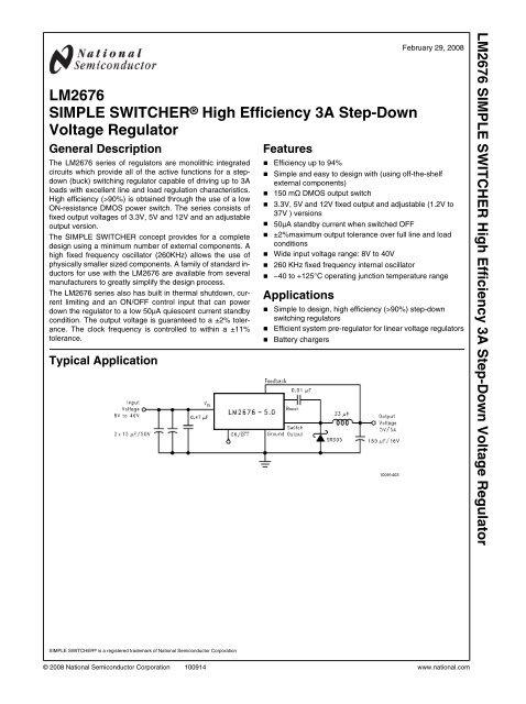
Typical Application<br />
Features<br />
February 29, 2008<br />
■ Efficiency up to 94%<br />
■ Simple and easy to design with (using off-the-shelf<br />
external components)<br />
■ 150 mΩ DMOS output switch<br />
■ 3.3V, 5V and 12V fixed output and adjustable (1.2V to<br />
37V ) versions<br />
■ 50μA standby current when switched OFF<br />
■ ±2%maximum output tolerance over full line and load<br />
conditions<br />
■ Wide input voltage range: 8V to 40V<br />
■ 260 KHz fixed frequency internal oscillator<br />
■ −40 to +125°C operating junction temperature range<br />
Applications<br />
■ Simple to design, high efficiency (>90%) step-down<br />
switching regulators<br />
■ Efficient system pre-regulator for linear voltage regulators<br />
■ Battery chargers<br />
10091403<br />
<strong>LM2676</strong> SIMPLE SWITCHER High Efficiency 3A Step-Down Voltage Regulator<br />
SIMPLE SWITCHER ® is a registered trademark of National Semiconductor Corporation<br />
© 2008 National Semiconductor Corporation 100914 www.national.com
<strong>LM2676</strong><br />
Connection Diagrams and Ordering Information<br />
TO-263 Package<br />
Top View<br />
TO-220 Package<br />
Top View<br />
Order Number<br />
<strong>LM2676</strong>S-3.3, <strong>LM2676</strong>S-5.0,<br />
<strong>LM2676</strong>S-12 or <strong>LM2676</strong>S-ADJ<br />
See NSC Package Number TS7B<br />
10091401<br />
Order Number<br />
<strong>LM2676</strong>T-3.3, <strong>LM2676</strong>T-5.0,<br />
<strong>LM2676</strong>T-12 or <strong>LM2676</strong>T-ADJ<br />
See NSC Package Number TA07B<br />
10091402<br />
Top View<br />
LLP-14<br />
See NS package Number SRC14A<br />
10091441<br />
Ordering Information for LLP Package<br />
Output Voltage Order Information Package Marking Supplied As<br />
12 <strong>LM2676</strong>SD-12 S0003LB 250 Units on Tape and Reel<br />
12 <strong>LM2676</strong>SDX-12 S0003LB 2500 Units on Tape and Reel<br />
3.3 <strong>LM2676</strong>SD-3.3 S0003NB 250 Units on Tape and Reel<br />
3.3 <strong>LM2676</strong>SDX-3.3 S0003NB 2500 Units on Tape and Reel<br />
5.0 <strong>LM2676</strong>SD-5.0 S0003PB 250 Units on Tape and Reel<br />
5.0 <strong>LM2676</strong>SDX-5.0 S0003PB 2500 Units on Tape and Reel<br />
ADJ <strong>LM2676</strong>SD-ADJ S0003RB 250 Units on Tape and Reel<br />
ADJ <strong>LM2676</strong>SDX-ADJ S0003RB 2500 Units on Tape and Reel<br />
www.national.com 2
Absolute Maximum Ratings (Note 1)<br />
If Military/Aerospace specified devices are required,<br />
please contact the National Semiconductor Sales Office/<br />
Distributors for availability and specifications.<br />
Input Supply Voltage<br />
ON/OFF Pin Voltage<br />
Switch Voltage to Ground (Note 12)<br />
Boost Pin Voltage<br />
Feedback Pin Voltage<br />
Power Dissipation<br />
45V<br />
−0.1V to 6V<br />
−1V to V IN<br />
V SW + 8V<br />
−0.3V to 14V<br />
Internally Limited<br />
ESD (Note 2)<br />
2 kV<br />
Storage Temperature Range −65°C to 150°C<br />
Soldering Temperature<br />
Wave 4 sec, 260°C<br />
Infrared 10 sec, 240°C<br />
Vapor Phase 75 sec, 219°C<br />
Operating Ratings<br />
Supply Voltage<br />
8V to 40V<br />
Junction Temperature Range (T J ) −40°C to 125°C<br />
<strong>LM2676</strong><br />
Electrical Characteristics Limits appearing in bold type face apply over the entire junction temperature range<br />
of operation, −40°C to 125°C. Specifications appearing in normal type apply for T A = T J = 25°C.<br />
<strong>LM2676</strong>-3.3<br />
Symbol Parameter Conditions Typical Min Max Units<br />
(Note 3) (Note 4) (Note 4)<br />
V OUT Output Voltage V IN = 8V to 40V, 100mA ≤ I OUT ≤ 3A 3.3 3.234/3.201 3.366/3.399 V<br />
η Efficiency V IN = 12V, I LOAD = 3A 86 %<br />
<strong>LM2676</strong>-5.0<br />
Symbol Parameter Conditions Typical Min Max Units<br />
(Note 3) (Note 4) (Note 4)<br />
V OUT Output Voltage V IN = 8V to 40V, 100mA ≤ I OUT ≤ 3A 5.0 4.900/4.850 5.100/5.150 V<br />
η Efficiency V IN = 12V, I LOAD = 3A 88 %<br />
<strong>LM2676</strong>-12<br />
Symbol Parameter Conditions Typical Min Max Units<br />
(Note 3) (Note 4) (Note 4)<br />
V OUT Output Voltage V IN = 15V to 40V, 100mA ≤ I OUT ≤ 3A 12 11.76/11.64 12.24/12.36 V<br />
η Efficiency V IN = 24V, I LOAD = 3A 94 %<br />
<strong>LM2676</strong>-ADJ<br />
Symbol Parameter Conditions Typ Min Max Units<br />
V FB Feedback Voltage V IN = 8V to 40V, 100mA ≤ I OUT ≤ 3A<br />
V OUT Programmed for 5V<br />
(Note 3) (Note 4) (Note 4)<br />
1.21 1.186/1.174 1.234/1.246 V<br />
η Efficiency V IN = 12V, I LOAD = 3A 88 %<br />
3 www.national.com
<strong>LM2676</strong><br />
All Output Voltage Versions<br />
Electrical Characteristics<br />
Limits appearing in bold type face apply over the entire junction temperature range of operation, −40°C to 125°C.<br />
Specifications appearing in normal type apply for T A = T J = 25°C. Unless otherwise specified V IN =12V for the 3.3V, 5V and Adjustable<br />
versions and V IN =24V for the 12V version.<br />
Symbol Parameter Conditions Typ Min Max Units<br />
DEVICE PARAMETERS<br />
I Q Quiescent Current V FEEDBACK = 8V 4.2 6 mA<br />
I STBY<br />
Standby Quiescent<br />
Current<br />
For 3.3V, 5.0V, and ADJ Versions<br />
V FEEDBACK = 15V<br />
For 12V Versions<br />
ON/OFF Pin = 0V<br />
50 100/150 μA<br />
I CL Current Limit 4.5 3.8/3.6 5.25/5.4 A<br />
I L<br />
R DS(ON)<br />
f O<br />
Output Leakage<br />
Current<br />
Switch On-<br />
Resistance<br />
Oscillator<br />
Frequency<br />
V IN = 40V, ON/OFF Pin = 0V<br />
V SWITCH = 0V<br />
V SWITCH = −1V 16<br />
I SWITCH = 3A 0.15 0.17/0.29 Ω<br />
Measured at Switch Pin 260 225 280 kHz<br />
D Duty Cycle Maximum Duty Cycle 91 %<br />
I BIAS<br />
V ON/OFF<br />
I ON/OFF<br />
θ JA<br />
Feedback Bias<br />
Current<br />
ON/OFF<br />
Threshold Voltage<br />
ON/OFF Input<br />
Current<br />
Thermal<br />
Resistance<br />
Minimum Duty Cycle 0 %<br />
V FEEDBACK = 1.3V<br />
ADJ Version Only<br />
ON/OFF Input = 0V<br />
T Package, Junction to Ambient 65<br />
(Note 5)<br />
θ JA<br />
T Package, Junction to Ambient 45<br />
(Note 6)<br />
θ JC<br />
T Package, Junction to Case 2<br />
200<br />
15<br />
μA<br />
mA<br />
85 nA<br />
1.4 0.8 2.0 V<br />
20 45 μA<br />
θ JA<br />
S Package, Junction to Ambient 56 °C/W<br />
(Note 7)<br />
θ JA<br />
S Package, Junction to Ambient 35<br />
(Note 8)<br />
θ JA<br />
S Package, Junction to Ambient 26<br />
(Note 9)<br />
θ JC<br />
S Package, Junction to Case 2 ++<br />
θ JA<br />
SD Package, Junction to Ambient 55<br />
(Note 10)<br />
θ JA<br />
SD Package, Junction to Ambient 29<br />
(Note 11)<br />
°C/W<br />
www.national.com 4
Note 1: Absolute Maximum Ratings are limits beyond which damage to the device may occur. Operating Ratings indicate conditions under which of the device<br />
is guaranteed. Operating Ratings do not imply guaranteed performance limits. For guaranteed performance limits and associated test condition, see the electrical<br />
Characteristics tables.<br />
Note 2: ESD was applied using the human-body model, a 100pF capacitor discharged through a 1.5 kΩ resistor into each pin.<br />
Note 3: Typical values are determined with T A = T J = 25°C and represent the most likely norm.<br />
Note 4: All limits are guaranteed at room temperature (standard type face) and at temperature extremes (bold type face). All room temperature limits are 100%<br />
tested during production with T A = T J = 25°C. All limits at temperature extremes are guaranteed via correlation using standard standard Quality Control (SQC)<br />
methods. All limits are used to calculate Average Outgoing Quality Level (AOQL).<br />
Note 5: Junction to ambient thermal resistance (no external heat sink) for the 7 lead TO-220 package mounted vertically, with ½ inch leads in a socket, or on a<br />
PC board with minimum copper area.<br />
Note 6: Junction to ambient thermal resistance (no external heat sink) for the 7 lead TO-220 package mounted vertically, with ½ inch leads soldered to a PC<br />
board containing approximately 4 square inches of (1 oz.) copper area surrounding the leads.<br />
Note 7: Junction to ambient thermal resistance for the 7 lead TO-263 mounted horizontally against a PC board area of 0.136 square inches (the same size as<br />
the TO-263 package) of 1 oz. (0.0014 in. thick) copper.<br />
Note 8: Junction to ambient thermal resistance for the 7 lead TO-263 mounted horizontally against a PC board area of 0.4896 square inches (3.6 times the area<br />
of the TO-263 package) of 1 oz. (0.0014 in. thick) copper.<br />
Note 9: Junction to ambient thermal resistance for the 7 lead TO-263 mounted horizontally against a PC board copper area of 1.0064 square inches (7.4 times<br />
the area of the TO-263 package) of 1 oz. (0.0014 in. thick) copper. Additional copper area will reduce thermal resistance further. See the thermal model in Switchers<br />
Made Simple ® software.<br />
Note 10: Junction to ambient thermal resistance for the 14-lead LLP mounted on a PC board copper area equal to the die attach paddle.<br />
Note 11: Junction to ambient thermal resistance for the 14-lead LLP mounted on a PC board copper area using 12 vias to a second layer of copper equal to die<br />
attach paddle. Additional copper area will reduce thermal resistance further. For layout recommendations, refer to Application Note AN-1187.<br />
Note 12: The absolute maximum specification of the 'Switch Voltage to Ground' applies to DC voltage. An extended negative voltage limit of -8V applies to a<br />
pulse of up to 20 ns, -6V of 60 ns and -3V of up to 100 ns.<br />
<strong>LM2676</strong><br />
5 www.national.com
<strong>LM2676</strong><br />
Typical Performance Characteristics<br />
Normalized<br />
Output Voltage<br />
Line Regulation<br />
10091409<br />
10091410<br />
Efficiency vs Input Voltage<br />
Efficiency vs I LOAD<br />
10091412<br />
10091411<br />
Switch Current Limit<br />
Operating Quiescent Current<br />
10091404<br />
10091405<br />
www.national.com 6
Standby Quiescent Current<br />
ON/OFF Threshold Voltage<br />
<strong>LM2676</strong><br />
ON/OFF Pin Current (Sourcing)<br />
10091440<br />
Switching Frequency<br />
10091413<br />
Feedback Pin Bias Current<br />
10091414<br />
10091415<br />
10091416<br />
7 www.national.com
<strong>LM2676</strong><br />
Typical Performance Characteristics<br />
Continuous Mode Switching Waveforms<br />
V IN = 20V, V OUT = 5V, I LOAD = 3A<br />
L = 33 μH, C OUT = 200 μF, C OUT ESR = 26 mΩ<br />
Discontinuous Mode Switching Waveforms<br />
V IN = 20V, V OUT = 5V, I LOAD = 500 mA<br />
L = 10 μH, C OUT = 400 μF, C OUT ESR = 13 mΩ<br />
10091417<br />
A: V SW Pin Voltage, 10 V/div.<br />
B: Inductor Current, 1 A/div<br />
C: Output Ripple Voltage, 20 mV/div AC-Coupled<br />
Horizontal Time Base: 1 μs/div<br />
10091418<br />
A: V SW Pin Voltage, 10 V/div.<br />
B: Inductor Current, 1 A/div<br />
C: Output Ripple Voltage, 20 mV/div AC-Coupled<br />
Horizontal Time Base: 1 μs//iv<br />
Load Transient Response for Continuous Mode<br />
V IN = 20V, V OUT = 5V<br />
L = 33 μH, C OUT = 200 μF, C OUT ESR = 26 mΩ<br />
Load Transient Response for Discontinuous Mode<br />
V IN = 20V, V OUT = 5V,<br />
L = 10 μH, C OUT = 400 μF, C OUT ESR = 13 mΩ<br />
10091419<br />
A: Output Voltage, 100 mV//div, AC-Coupled.<br />
B: Load Current: 500 mA to 3A Load Pulse<br />
Horizontal Time Base: 100 μs/div<br />
10091420<br />
A: Output Voltage, 100 mV/div, AC-Coupled.<br />
B: Load Current: 200 mA to 3A Load Pulse<br />
Horizontal Time Base: 200 μs/div<br />
www.national.com 8
Block Diagram<br />
<strong>LM2676</strong><br />
* Active Inductor Patent Number 5,514,947<br />
† Active Capacitor Patent Number 5,382,918<br />
10091406<br />
9 www.national.com
<strong>LM2676</strong><br />
Application Hints<br />
The <strong>LM2676</strong> provides all of the active functions required for<br />
a step-down (buck) switching regulator. The internal power<br />
switch is a DMOS power MOSFET to provide power supply<br />
designs with high current capability, up to 3A, and highly efficient<br />
operation.<br />
The <strong>LM2676</strong> is part of the SIMPLE SWITCHER family of<br />
power converters. A complete design uses a minimum number<br />
of external components, which have been pre-determined<br />
from a variety of manufacturers. Using either this data sheet<br />
or a design software program called LM267X Made Simple<br />
(version 2.0) a complete switching power supply can be designed<br />
quickly. The software is provided free of charge and<br />
can be downloaded from National Semiconductor's Internet<br />
site located at http://www.national.com.<br />
SWITCH OUTPUT<br />
This is the output of a power MOSFET switch connected directly<br />
to the input voltage. The switch provides energy to an<br />
inductor, an output capacitor and the load circuitry under control<br />
of an internal pulse-width-modulator (PWM). The PWM<br />
controller is internally clocked by a fixed 260KHz oscillator. In<br />
a standard step-down application the duty cycle (Time ON/<br />
Time OFF) of the power switch is proportional to the ratio of<br />
the power supply output voltage to the input voltage. The voltage<br />
on pin 1 switches between Vin (switch ON) and below<br />
ground by the voltage drop of the external Schottky diode<br />
(switch OFF).<br />
INPUT<br />
The input voltage for the power supply is connected to pin 2.<br />
In addition to providing energy to the load the input voltage<br />
also provides bias for the internal circuitry of the <strong>LM2676</strong>. For<br />
guaranteed performance the input voltage must be in the<br />
range of 8V to 40V. For best performance of the power supply<br />
the input pin should always be bypassed with an input capacitor<br />
located close to pin 2.<br />
C BOOST<br />
A capacitor must be connected from pin 3 to the switch output,<br />
pin 1. This capacitor boosts the gate drive to the internal<br />
DESIGN CONSIDERATIONS<br />
MOSFET above Vin to fully turn it ON. This minimizes conduction<br />
losses in the power switch to maintain high efficiency.<br />
The recommended value for C Boost is 0.01μF.<br />
GROUND<br />
This is the ground reference connection for all components in<br />
the power supply. In fast-switching, high-current applications<br />
such as those implemented with the <strong>LM2676</strong>, it is recommended<br />
that a broad ground plane be used to minimize signal<br />
coupling throughout the circuit<br />
FEEDBACK<br />
This is the input to a two-stage high gain amplifier, which<br />
drives the PWM controller. It is necessary to connect pin 6 to<br />
the actual output of the power supply to set the dc output voltage.<br />
For the fixed output devices (3.3V, 5V and 12V outputs),<br />
a direct wire connection to the output is all that is required as<br />
internal gain setting resistors are provided inside the <strong>LM2676</strong>.<br />
For the adjustable output version two external resistors are<br />
required to set the dc output voltage. For stable operation of<br />
the power supply it is important to prevent coupling of any<br />
inductor flux to the feedback input.<br />
ON/OFF<br />
This input provides an electrical ON/OFF control of the power<br />
supply. Connecting this pin to ground or to any voltage less<br />
than 0.8V will completely turn OFF the regulator. The current<br />
drain from the input supply when OFF is only 50μA. Pin 7 has<br />
an internal pull-up current source of approximately 20μA and<br />
a protection clamp zener diode of 7V to ground. When electrically<br />
driving the ON/OFF pin the high voltage level for the<br />
ON condition should not exceed the 6V absolute maximum<br />
limit. When ON/OFF control is not required pin 7 should be<br />
left open circuited.<br />
DAP (LLP PACKAGE)<br />
The Die Attach Pad (DAP) can and should be connected to<br />
PCB Ground plane/island. For CAD and assembly guidelines<br />
refer to Application Note AN-1187 at http://<br />
power.national.com.<br />
10091407<br />
FIGURE 1. Basic circuit for fixed output voltage applications.<br />
www.national.com 10
<strong>LM2676</strong><br />
10091408<br />
FIGURE 2. Basic circuit for adjustable output voltage applications<br />
Power supply design using the <strong>LM2676</strong> is greatly simplified<br />
by using recommended external components. A wide range<br />
of inductors, capacitors and Schottky diodes from several<br />
manufacturers have been evaluated for use in designs that<br />
cover the full range of capabilities (input voltage, output voltage<br />
and load current) of the <strong>LM2676</strong>. A simple design procedure<br />
using nomographs and component tables provided in<br />
this data sheet leads to a working design with very little effort.<br />
Alternatively, the design software, LM267X Made Simple<br />
(version 6.0), can also be used to provide instant component<br />
selection, circuit performance calculations for evaluation, a<br />
bill of materials component list and a circuit schematic.<br />
INDUCTOR<br />
The inductor is the key component in a switching regulator.<br />
For efficiency the inductor stores energy during the switch ON<br />
time and then transfers energy to the load while the switch is<br />
OFF.<br />
Nomographs are used to select the inductance value required<br />
for a given set of operating conditions. The nomographs assume<br />
that the circuit is operating in continuous mode (the<br />
current flowing through the inductor never falls to zero). The<br />
magnitude of inductance is selected to maintain a maximum<br />
ripple current of 30% of the maximum load current. If the ripple<br />
current exceeds this 30% limit the next larger value is selected.<br />
The inductors offered have been specifically manufactured to<br />
provide proper operation under all operating conditions of input<br />
and output voltage and load current. Several part types<br />
are offered for a given amount of inductance. Both surface<br />
mount and through-hole devices are available. The inductors<br />
from each of the three manufacturers have unique characteristics.<br />
Renco: ferrite stick core inductors; benefits are typically lowest<br />
cost and can withstand ripple and transient peak currents<br />
above the rated value. These inductors have an external<br />
magnetic field, which may generate EMI.<br />
Pulse Engineering: powdered iron toroid core inductors;<br />
these also can withstand higher than rated currents and, being<br />
toroid inductors, will have low EMI.<br />
Coilcraft: ferrite drum core inductors; these are the smallest<br />
physical size inductors and are available only as surface<br />
mount components. These inductors also generate EMI but<br />
less than stick inductors.<br />
The individual components from the various manufacturers<br />
called out for use are still just a small sample of the vast array<br />
of components available in the industry. While these components<br />
are recommended, they are not exclusively the only<br />
components for use in a design. After a close comparison of<br />
component specifications, equivalent devices from other<br />
manufacturers could be substituted for use in an application.<br />
Important considerations for each external component and an<br />
explanation of how the nomographs and selection tables were<br />
developed follows.<br />
OUTPUT CAPACITOR<br />
The output capacitor acts to smooth the dc output voltage and<br />
also provides energy storage. Selection of an output capacitor,<br />
with an associated equivalent series resistance (ESR),<br />
impacts both the amount of output ripple voltage and stability<br />
of the control loop.<br />
The output ripple voltage of the power supply is the product<br />
of the capacitor ESR and the inductor ripple current. The capacitor<br />
types recommended in the tables were selected for<br />
having low ESR ratings.<br />
In addition, both surface mount tantalum capacitors and<br />
through-hole aluminum electrolytic capacitors are offered as<br />
solutions.<br />
Impacting frequency stability of the overall control loop, the<br />
output capacitance, in conjunction with the inductor, creates<br />
a double pole inside the feedback loop. In addition the capacitance<br />
and the ESR value create a zero. These frequency<br />
response effects together with the internal frequency compensation<br />
circuitry of the <strong>LM2676</strong> modify the gain and phase<br />
shift of the closed loop system.<br />
As a general rule for stable switching regulator circuits it is<br />
desired to have the unity gain bandwidth of the circuit to be<br />
limited to no more than one-sixth of the controller switching<br />
frequency. With the fixed 260KHz switching frequency of the<br />
<strong>LM2676</strong>, the output capacitor is selected to provide a unity<br />
gain bandwidth of 40KHz maximum. Each recommended capacitor<br />
value has been chosen to achieve this result.<br />
In some cases multiple capacitors are required either to reduce<br />
the ESR of the output capacitor, to minimize output<br />
ripple (a ripple voltage of 1% of Vout or less is the assumed<br />
performance condition), or to increase the output capacitance<br />
11 www.national.com
<strong>LM2676</strong><br />
to reduce the closed loop unity gain bandwidth (to less than<br />
40KHz). When parallel combinations of capacitors are required<br />
it has been assumed that each capacitor is the exact<br />
same part type.<br />
The RMS current and working voltage (WV) ratings of the<br />
output capacitor are also important considerations. In a typical<br />
step-down switching regulator, the inductor ripple current<br />
(set to be no more than 30% of the maximum load current by<br />
the inductor selection) is the current that flows through the<br />
output capacitor. The capacitor RMS current rating must be<br />
greater than this ripple current. The voltage rating of the output<br />
capacitor should be greater than 1.3 times the maximum<br />
output voltage of the power supply. If operation of the system<br />
at elevated temperatures is required, the capacitor voltage<br />
rating may be de-rated to less than the nominal room temperature<br />
rating. Careful inspection of the manufacturer's<br />
specification for de-rating of working voltage with temperature<br />
is important.<br />
INPUT CAPACITOR<br />
Fast changing currents in high current switching regulators<br />
place a significant dynamic load on the unregulated power<br />
source. An input capacitor helps to provide additional current<br />
to the power supply as well as smooth out input voltage variations.<br />
Like the output capacitor, the key specifications for the input<br />
capacitor are RMS current rating and working voltage. The<br />
RMS current flowing through the input capacitor is equal to<br />
one-half of the maximum dc load current so the capacitor<br />
should be rated to handle this. Paralleling multiple capacitors<br />
proportionally increases the current rating of the total capacitance.<br />
The voltage rating should also be selected to be 1.3<br />
times the maximum input voltage. Depending on the unregulated<br />
input power source, under light load conditions the<br />
maximum input voltage could be significantly higher than normal<br />
operation and should be considered when selecting an<br />
input capacitor.<br />
The input capacitor should be placed very close to the input<br />
pin of the <strong>LM2676</strong>. Due to relative high current operation with<br />
fast transient changes, the series inductance of input connecting<br />
wires or PCB traces can create ringing signals at the<br />
input terminal which could possibly propagate to the output or<br />
other parts of the circuitry. It may be necessary in some designs<br />
to add a small valued (0.1μF to 0.47μF) ceramic type<br />
capacitor in parallel with the input capacitor to prevent or minimize<br />
any ringing.<br />
CATCH DIODE<br />
When the power switch in the <strong>LM2676</strong> turns OFF, the current<br />
through the inductor continues to flow. The path for this current<br />
is through the diode connected between the switch output<br />
and ground. This forward biased diode clamps the switch output<br />
to a voltage less than ground. This negative voltage must<br />
be greater than −1V so a low voltage drop (particularly at high<br />
current levels) Schottky diode is recommended. Total efficiency<br />
of the entire power supply is significantly impacted by<br />
the power lost in the output catch diode. The average current<br />
through the catch diode is dependent on the switch duty cycle<br />
(D) and is equal to the load current times (1-D). Use of a diode<br />
rated for much higher current than is required by the actual<br />
application helps to minimize the voltage drop and power loss<br />
in the diode.<br />
During the switch ON time the diode will be reversed biased<br />
by the input voltage. The reverse voltage rating of the diode<br />
should be at least 1.3 times greater than the maximum input<br />
voltage.<br />
BOOST CAPACITOR<br />
The boost capacitor creates a voltage used to overdrive the<br />
gate of the internal power MOSFET. This improves efficiency<br />
by minimizing the on resistance of the switch and associated<br />
power loss. For all applications it is recommended to use a<br />
0.01μF/50V ceramic capacitor.<br />
ADDITIONAL APPLICATON INFORMATION<br />
When the output voltage is greater than approximately 6V,<br />
and the duty cycle at minimum input voltage is greater than<br />
approximately 50%, the designer should exercise caution in<br />
selection of the output filter components. When an application<br />
designed to these specific operating conditions is subjected<br />
to a current limit fault condition, it may be possible to observe<br />
a large hysteresis in the current limit. This can affect the output<br />
voltage of the device until the load current is reduced<br />
sufficiently to allow the current limit protection circuit to reset<br />
itself.<br />
Under current limiting conditions, the LM267x is designed to<br />
respond in the following manner:<br />
1. At the moment when the inductor current reaches the<br />
current limit threshold, the ON-pulse is immediately<br />
terminated. This happens for any application condition.<br />
2. However, the current limit block is also designed to<br />
momentarily reduce the duty cycle to below 50% to avoid<br />
subharmonic oscillations, which could cause the inductor<br />
to saturate.<br />
3. Thereafter, once the inductor current falls below the<br />
current limit threshold, there is a small relaxation time<br />
during which the duty cycle progressively rises back<br />
above 50% to the value required to achieve regulation.<br />
If the output capacitance is sufficiently ‘large’, it may be possible<br />
that as the output tries to recover, the output capacitor<br />
charging current is large enough to repeatedly re-trigger the<br />
current limit circuit before the output has fully settled. This<br />
condition is exacerbated with higher output voltage settings<br />
because the energy requirement of the output capacitor<br />
varies as the square of the output voltage (½CV 2 ), thus requiring<br />
an increased charging current.<br />
A simple test to determine if this condition might exist for a<br />
suspect application is to apply a short circuit across the output<br />
of the converter, and then remove the shorted output condition.<br />
In an application with properly selected external components,<br />
the output will recover smoothly.<br />
Practical values of external components that have been experimentally<br />
found to work well under these specific operating<br />
conditions are C OUT = 47µF, L = 22µH. It should be noted that<br />
even with these components, for a device’s current limit of<br />
I CLIM , the maximum load current under which the possibility of<br />
the large current limit hysteresis can be minimized is I CLIM /2.<br />
For example, if the input is 24V and the set output voltage is<br />
18V, then for a desired maximum current of 1.5A, the current<br />
limit of the chosen switcher must be confirmed to be at least<br />
3A.<br />
SIMPLE DESIGN PROCEDURE<br />
Using the nomographs and tables in this data sheet (or use<br />
the available design software at http://www.national.com) a<br />
complete step-down regulator can be designed in a few simple<br />
steps.<br />
Step 1: Define the power supply operating conditions:<br />
Required output voltage<br />
Maximum DC input voltage<br />
Maximum output load current<br />
www.national.com 12
Step 2: Set the output voltage by selecting a fixed output<br />
<strong>LM2676</strong> (3.3V, 5V or 12V applications) or determine the required<br />
feedback resistors for use with the adjustable <strong>LM2676</strong><br />
−ADJ<br />
Step 3: Determine the inductor required by using one of the<br />
four nomographs, Figure 3 through Figure 6. Table 1 provides<br />
a specific manufacturer and part number for the inductor.<br />
Step 4: Using Table 3 (fixed output voltage) or Table 6 (adjustable<br />
output voltage), determine the output capacitance<br />
required for stable operation. Table 2 provides the specific<br />
capacitor type from the manufacturer of choice.<br />
Step 5: Determine an input capacitor from Table 4 for fixed<br />
output voltage applications. Use Table 2 to find the specific<br />
capacitor type. For adjustable output circuits select a capacitor<br />
from Table 2 with a sufficient working voltage (WV) rating<br />
greater than Vin max, and an rms current rating greater than<br />
one-half the maximum load current (2 or more capacitors in<br />
parallel may be required).<br />
Step 6: Select a diode from Table 5. The current rating of the<br />
diode must be greater than I load max and the Reverse Voltage<br />
rating must be greater than Vin max.<br />
Step 7: Include a 0.01μF/50V capacitor for Cboost in the design.<br />
FIXED OUTPUT VOLTAGE DESIGN EXAMPLE<br />
A system logic power supply bus of 3.3V is to be generated<br />
from a wall adapter which provides an unregulated DC voltage<br />
of 13V to 16V. The maximum load current is 2.5A.<br />
Through-hole components are preferred.<br />
Step 1: Operating conditions are:<br />
Vout = 3.3V<br />
Vin max = 16V<br />
Iload max = 2.5A<br />
Step 2: Select an <strong>LM2676</strong>T-3.3. The output voltage will have<br />
a tolerance of<br />
±2% at room temperature and ±3% over the full operating<br />
temperature range.<br />
Step 3: Use the nomograph for the 3.3V device ,Figure 3. The<br />
intersection of the 16V horizontal line (V in max) and the 2.5A<br />
vertical line (I load max) indicates that L33, a 22μH inductor, is<br />
required.<br />
From Table 1, L33 in a through-hole component is available<br />
from Renco with part number RL-1283-22-43 or part number<br />
PE-53933 from Pulse Engineering.<br />
Step 4: Use Table 3 to determine an output capacitor. With a<br />
3.3V output and a 22μH inductor there are four through-hole<br />
output capacitor solutions with the number of same type capacitors<br />
to be paralleled and an identifying capacitor code<br />
given. Table 2 provides the actual capacitor characteristics.<br />
Any of the following choices will work in the circuit:<br />
1 x 220μF/10V Sanyo OS-CON (code C5)<br />
1 x 1000μF/35V Sanyo MV-GX (code C10)<br />
1 x 2200μF/10V Nichicon PL (code C5)<br />
1 x 1000μF/35V Panasonic HFQ (code C7)<br />
Step 5: Use Table 4 to select an input capacitor. With 3.3V<br />
output and 22μH there are three through-hole solutions.<br />
These capacitors provide a sufficient voltage rating and an<br />
rms current rating greater than 1.25A (1/2 I load max). Again<br />
using Table 2 for specific component characteristics the following<br />
choices are suitable:<br />
1 x 1000μF/63V Sanyo MV-GX (code C14)<br />
1 x 820μF/63V Nichicon PL (code C24)<br />
1 x 560μF/50V Panasonic HFQ (code C13)<br />
Step 6: From Table 5 a 3A Schottky diode must be selected.<br />
For through-hole components 20V rated diodes are sufficient<br />
and 2 part types are suitable:<br />
1N5820<br />
SR302<br />
Step 7: A 0.01μF capacitor will be used for Cboost.<br />
ADJUSTABLE OUTPUT DESIGN EXAMPLE<br />
In this example it is desired to convert the voltage from a two<br />
battery automotive power supply (voltage range of 20V to<br />
28V, typical in large truck applications) to the 14.8VDC alternator<br />
supply typically used to power electronic equipment<br />
from single battery 12V vehicle systems. The load current required<br />
is 2A maximum. It is also desired to implement the<br />
power supply with all surface mount components.<br />
Step 1: Operating conditions are:<br />
Vout = 14.8V<br />
Vin max = 28V<br />
Iload max = 2A<br />
Step 2: Select an <strong>LM2676</strong>S-ADJ. To set the output voltage<br />
to 14.9V two resistors need to be chosen (R1 and R2 in Figure<br />
2). For the adjustable device the output voltage is set by the<br />
following relationship:<br />
Where V FB is the feedback voltage of typically 1.21V.<br />
A recommended value to use for R1 is 1K. In this example<br />
then R2 is determined to be:<br />
R2 = 11.23KΩ<br />
The closest standard 1% tolerance value to use is 11.3KΩ<br />
This will set the nominal output voltage to 14.88V which is<br />
within 0.5% of the target value.<br />
Step 3: To use the nomograph for the adjustable device, Figure<br />
6, requires a calculation of the inductor Volt•microsecond<br />
constant (E•T expressed in V•μS) from the following formula:<br />
where V SAT is the voltage drop across the internal power<br />
switch which is R ds(ON) times I load . In this example this would<br />
be typically 0.15Ω x 2A or 0.3V and V D is the voltage drop<br />
across the forward bisased Schottky diode, typically 0.5V.<br />
The switching frequency of 260KHz is the nominal value to<br />
use to estimate the ON time of the switch during which energy<br />
is stored in the inductor.<br />
For this example E•T is found to be:<br />
Using Figure 6, the intersection of 27V•μS horizontally and<br />
the 2A vertical line (I load max) indicates that L38 , a 68μH inductor,<br />
should be used.<br />
<strong>LM2676</strong><br />
13 www.national.com
<strong>LM2676</strong><br />
From Table 1, L38 in a surface mount component is available<br />
from Pulse Engineering with part number PE-54038S.<br />
Step 4: Use Table 6 to determine an output capacitor. With a<br />
14.8V output the 12.5 to 15V row is used and with a 68μH<br />
inductor there are three surface mount output capacitor solutions.<br />
Table 2 provides the actual capacitor characteristics<br />
based on the C Code number. Any of the following choices<br />
can be used:<br />
1 x 33μF/20V AVX TPS (code C6)<br />
1 x 47μF/20V Sprague 594 (code C8)<br />
1 x 47μF/20V Kemet T495 (code C8)<br />
Important Note: When using the adjustable device in low<br />
voltage applications (less than 3V output), if the nomograph,<br />
Figure 6, selects an inductance of 22μH or less, Table 6 does<br />
not provide an output capacitor solution. With these conditions<br />
the number of output capacitors required for stable<br />
operation becomes impractical. It is recommended to use either<br />
a 33μH or 47μH inductor and the output capacitors from<br />
Table 6.<br />
Step 5: An input capacitor for this example will require at least<br />
a 35V WV rating with an rms current rating of 1A (1/2 Iout<br />
max). From Table 2 it can be seen that C12, a 33μF/35V capacitor<br />
from Sprague, has the required voltage/current rating<br />
of the surface mount components.<br />
Step 6: From Table 5 a 3A Schottky diode must be selected.<br />
For surface mount diodes with a margin of safety on the voltage<br />
rating one of five diodes can be used:<br />
SK34<br />
30BQ040<br />
30WQ04F<br />
MBRS340<br />
MBRD340<br />
Step 7: A 0.01μF capacitor will be used for Cboost.<br />
LLP PACKAGE DEVICES<br />
The <strong>LM2676</strong> is offered in the 14 lead LLP surface mount<br />
package to allow for a significantly decreased footprint with<br />
equivalent power dissipation compared to the TO-263. For<br />
details on mounting and soldering specifications, refer to Application<br />
Note AN-1187.<br />
www.national.com 14
Inductor Selection Guides<br />
For Continuous Mode Operation<br />
<strong>LM2676</strong><br />
10091423<br />
10091421<br />
FIGURE 5. <strong>LM2676</strong>-12<br />
FIGURE 3. <strong>LM2676</strong>-3.3<br />
10091424<br />
FIGURE 4. <strong>LM2676</strong>-5.0<br />
10091422<br />
FIGURE 6. <strong>LM2676</strong>-ADJ<br />
15 www.national.com
<strong>LM2676</strong><br />
Inductor<br />
Reference<br />
Number<br />
Inductance<br />
(µH)<br />
Current<br />
(A)<br />
Table 1. Inductor Manufacturer Part Numbers<br />
Through Hole<br />
Renco Pulse Engineering Coilcraft<br />
Surface<br />
Mount<br />
Through<br />
Hole<br />
Surface<br />
Mount<br />
Surface Mount<br />
L23 33 1.35 RL-5471-7 RL1500-33 PE-53823 PE-53823S DO3316-333<br />
L24 22 1.65 RL-1283-22-43 RL1500-22 PE-53824 PE-53824S DO3316-223<br />
L25 15 2.00 RL-1283-15-43 RL1500-15 PE-53825 PE-53825S DO3316-153<br />
L29 100 1.41 RL-5471-4 RL-6050-100 PE-53829 PE-53829S DO5022P-104<br />
L30 68 1.71 RL-5471-5 RL6050-68 PE-53830 PE-53830S DO5022P-683<br />
L31 47 2.06 RL-5471-6 RL6050-47 PE-53831 PE-53831S DO5022P-473<br />
L32 33 2.46 RL-5471-7 RL6050-33 PE-53932 PE-53932S DO5022P-333<br />
L33 22 3.02 RL-1283-22-43 RL6050-22 PE-53933 PE-53933S DO5022P-223<br />
L34 15 3.65 RL-1283-15-43 — PE-53934 PE-53934S DO5022P-153<br />
L38 68 2.97 RL-5472-2 — PE-54038 PE-54038S —<br />
L39 47 3.57 RL-5472-3 — PE-54039 PE-54039S —<br />
L40 33 4.26 RL-1283-33-43 — PE-54040 PE-54040S —<br />
L41 22 5.22 RL-1283-22-43 — PE-54041 P0841 —<br />
L44 68 3.45 RL-5473-3 — PE-54044 — —<br />
L45 10 4.47 RL-1283-10-43 — — P0845 DO5022P-103HC<br />
Inductor Manufacturer Contact Numbers<br />
Coilcraft Phone (800) 322-2645<br />
FAX (708) 639-1469<br />
Coilcraft, Europe Phone +44 1236 730 595<br />
FAX +44 1236 730 627<br />
Pulse Engineering Phone (619) 674-8100<br />
FAX (619) 674-8262<br />
Pulse Engineering, Phone +353 93 24 107<br />
Europe FAX +353 93 24 459<br />
Renco Electronics Phone (800) 645-5828<br />
FAX (516) 586-5562<br />
www.national.com 16
Capacitor Selection Guides<br />
Table 2. Input and Output Capacitor Codes<br />
<strong>LM2676</strong><br />
Capacitor<br />
Reference<br />
Code<br />
Surface Mount<br />
AVX TPS Series Sprague 594D Series Kemet T495 Series<br />
C (µF) WV (V) Irms<br />
(A)<br />
C (µF) WV (V) Irms<br />
(A)<br />
C (µF) WV (V) Irms<br />
(A)<br />
C1 330 6.3 1.15 120 6.3 1.1 100 6.3 0.82<br />
C2 100 10 1.1 220 6.3 1.4 220 6.3 1.1<br />
C3 220 10 1.15 68 10 1.05 330 6.3 1.1<br />
C4 47 16 0.89 150 10 1.35 100 10 1.1<br />
C5 100 16 1.15 47 16 1 150 10 1.1<br />
C6 33 20 0.77 100 16 1.3 220 10 1.1<br />
C7 68 20 0.94 180 16 1.95 33 20 0.78<br />
C8 22 25 0.77 47 20 1.15 47 20 0.94<br />
C9 10 35 0.63 33 25 1.05 68 20 0.94<br />
C10 22 35 0.66 68 25 1.6 10 35 0.63<br />
C11 15 35 0.75 22 35 0.63<br />
C12 33 35 1 4.7 50 0.66<br />
C13 15 50 0.9<br />
Capacitor<br />
Reference<br />
Code<br />
Input and Output Capacitor Codes (continued)<br />
Through Hole<br />
Sanyo OS-CON SA Series Sanyo MV-GX Series Nichicon PL Series Panasonic HFQ Series<br />
C (µF) WV (V) Irms<br />
(A)<br />
C (µF) WV (V) Irms<br />
(A)<br />
C (µF) WV (V) Irms<br />
(A)<br />
C (µF) WV (V) Irms<br />
(A)<br />
C1 47 6.3 1 1000 6.3 0.8 680 10 0.8 82 35 0.4<br />
C2 150 6.3 1.95 270 16 0.6 820 10 0.98 120 35 0.44<br />
C3 330 6.3 2.45 470 16 0.75 1000 10 1.06 220 35 0.76<br />
C4 100 10 1.87 560 16 0.95 1200 10 1.28 330 35 1.01<br />
C5 220 10 2.36 820 16 1.25 2200 10 1.71 560 35 1.4<br />
C6 33 16 0.96 1000 16 1.3 3300 10 2.18 820 35 1.62<br />
C7 100 16 1.92 150 35 0.65 3900 10 2.36 1000 35 1.73<br />
C8 150 16 2.28 470 35 1.3 6800 10 2.68 2200 35 2.8<br />
C9 100 20 2.25 680 35 1.4 180 16 0.41 56 50 0.36<br />
C10 47 25 2.09 1000 35 1.7 270 16 0.55 100 50 0.5<br />
C11 220 63 0.76 470 16 0.77 220 50 0.92<br />
C12 470 63 1.2 680 16 1.02 470 50 1.44<br />
C13 680 63 1.5 820 16 1.22 560 50 1.68<br />
C14 1000 63 1.75 1800 16 1.88 1200 50 2.22<br />
C15 220 25 0.63 330 63 1.42<br />
C16 220 35 0.79 1500 63 2.51<br />
C17 560 35 1.43<br />
C18 2200 35 2.68<br />
C19 150 50 0.82<br />
C20 220 50 1.04<br />
C21 330 50 1.3<br />
C22 100 63 0.75<br />
C23 390 63 1.62<br />
C24 820 63 2.22<br />
C25 1200 63 2.51<br />
17 www.national.com
<strong>LM2676</strong><br />
Capacitor Manufacturer Contact Numbers<br />
Nichicon Phone (847) 843-7500<br />
FAX (847) 843-2798<br />
Panasonic Phone (714) 373-7857<br />
FAX (714) 373-7102<br />
AVX Phone (845) 448-9411<br />
FAX (845) 448-1943<br />
Sprague/Vishay Phone (207) 324-4140<br />
FAX (207) 324-7223<br />
Sanyo Phone (619) 661-6322<br />
FAX (619) 661-1055<br />
Kemet Phone (864) 963-6300<br />
FAX (864) 963-6521<br />
Table 3. Output Capacitors for Fixed Output Voltage Application<br />
Output<br />
Voltage (V)<br />
3.3<br />
5<br />
12<br />
Inductance<br />
(µH)<br />
Surface Mount<br />
AVX TPS Series Sprague 594D Series Kemet T495 Series<br />
No. C Code No. C Code No. C Code<br />
10 4 C2 3 C1 4 C4<br />
15 4 C2 3 C1 4 C4<br />
22 3 C2 2 C7 3 C4<br />
33 2 C2 2 C6 2 C4<br />
10 4 C2 4 C6 4 C4<br />
15 3 C2 2 C7 3 C4<br />
22 3 C2 2 C7 3 C4<br />
33 2 C2 2 C3 2 C4<br />
47 2 C2 1 C7 2 C4<br />
10 4 C5 3 C6 5 C9<br />
15 3 C5 2 C7 4 C8<br />
22 2 C5 2 C6 3 C8<br />
33 2 C5 1 C7 2 C8<br />
47 2 C4 1 C6 2 C8<br />
68 1 C5 1 C5 2 C7<br />
100 1 C4 1 C5 1 C8<br />
Output<br />
Voltage (V)<br />
3.3<br />
5<br />
Inductance<br />
(µH)<br />
Sanyo OS-CON SA<br />
Series<br />
Sanyo MV-GX Series<br />
Through Hole<br />
Nichicon PL Series<br />
Panasonic HFQ<br />
Series<br />
No. C Code No. C Code No. C Code No. C Code<br />
10 1 C3 1 C10 1 C6 2 C6<br />
15 1 C3 1 C10 1 C6 2 C5<br />
22 1 C5 1 C10 1 C5 1 C7<br />
33 1 C2 1 C10 1 C13 1 C5<br />
10 2 C4 1 C10 1 C6 2 C5<br />
15 1 C5 1 C10 1 C5 1 C6<br />
22 1 C5 1 C5 1 C5 1 C5<br />
33 1 C4 1 C5 1 C13 1 C5<br />
47 1 C4 1 C4 1 C13 2 C3<br />
www.national.com 18
Output<br />
Voltage (V)<br />
12<br />
Inductance<br />
(µH)<br />
Sanyo OS-CON SA<br />
Series<br />
Sanyo MV-GX Series<br />
Through Hole<br />
Nichicon PL Series<br />
Panasonic HFQ<br />
Series<br />
No. C Code No. C Code No. C Code No. C Code<br />
10 2 C7 1 C5 1 C18 2 C5<br />
15 1 C8 1 C5 1 C17 1 C5<br />
22 1 C7 1 C5 1 C13 1 C5<br />
33 1 C7 1 C3 1 C11 1 C4<br />
47 1 C7 1 C3 1 C10 1 C3<br />
68 1 C7 1 C2 1 C10 1 C3<br />
100 1 C7 1 C2 1 C9 1 C1<br />
<strong>LM2676</strong><br />
No. represents the number of identical capacitor types to be connected in parallel<br />
C Code indicates the Capacitor Reference number in Table 2 for identifying the specific component from the manufacturer.<br />
Table 4. Input Capacitors for Fixed Output Voltage Application<br />
(Assumes worst case maximum input voltage and load current for a given inductance value)<br />
Output<br />
Voltage (V)<br />
3.3<br />
5<br />
12<br />
Inductance<br />
(µH)<br />
Surface Mount<br />
AVX TPS Series Sprague 594D Series Kemet T495 Series<br />
No. C Code No. C Code No. C Code<br />
10 2 C5 1 C7 2 C8<br />
15 3 C9 1 C10 3 C10<br />
22 * * 2 C13 3 C12<br />
33 * * 2 C13 2 C12<br />
10 2 C5 1 C7 2 C8<br />
15 2 C5 1 C7 2 C8<br />
22 3 C10 2 C12 3 C11<br />
33 * * 2 C13 3 C12<br />
47 * * 1 C13 2 C12<br />
10 2 C7 2 C10 2 C7<br />
15 2 C7 2 C10 2 C7<br />
22 3 C10 2 C12 3 C10<br />
33 3 C10 2 C12 3 C10<br />
47 * * 2 C13 3 C12<br />
68 * * 2 C13 2 C12<br />
100 * * 1 C13 2 C12<br />
Output<br />
Voltage (V)<br />
3.3<br />
5<br />
Inductance<br />
(µH)<br />
Sanyo OS-CON SA<br />
Series<br />
Sanyo MV-GX Series<br />
Through Hole<br />
Nichicon PL Series<br />
Panasonic HFQ<br />
Series<br />
No. C Code No. C Code No. C Code No. C Code<br />
10 1 C7 2 C4 1 C5 1 C6<br />
15 1 C10 1 C10 1 C18 1 C6<br />
22 * * 1 C14 1 C24 1 C13<br />
33 * * 1 C12 1 C20 1 C12<br />
10 1 C7 2 C4 1 C14 1 C6<br />
15 1 C7 2 C4 1 C14 1 C6<br />
22 * * 1 C10 1 C18 1 C13<br />
33 * * 1 C14 1 C23 1 C13<br />
47 * * 1 C12 1 C20 1 C12<br />
19 www.national.com
<strong>LM2676</strong><br />
Output<br />
Voltage (V)<br />
12<br />
Inductance<br />
(µH)<br />
Sanyo OS-CON SA<br />
Series<br />
Sanyo MV-GX Series<br />
Through Hole<br />
Nichicon PL Series<br />
Panasonic HFQ<br />
Series<br />
No. C Code No. C Code No. C Code No. C Code<br />
10 1 C9 1 C10 1 C18 1 C6<br />
15 1 C10 1 C10 1 C18 1 C6<br />
22 1 C10 1 C10 1 C18 1 C6<br />
33 * * 1 C10 1 C18 1 C6<br />
47 * * 1 C13 1 C23 1 C13<br />
68 * * 1 C12 1 C21 1 C12<br />
100 * * 1 C11 1 C22 1 C11<br />
* Check voltage rating of capacitors to be greater than application input voltage.<br />
No. represents the number of identical capacitor types to be connected in parallel<br />
C Code indicates the Capacitor Reference number in Table 2 for identifying the specific component from the manufacturer.<br />
Reverse<br />
Voltage<br />
(V)<br />
Table 5. Schottky Diode Selection Table<br />
Surface Mount<br />
Through Hole<br />
3A 5A or More 3A 5A or More<br />
20V SK32 1N5820<br />
SR302<br />
30V SK33 MBRD835L 1N5821<br />
30WQ03F<br />
31DQ03<br />
40V SK34 MBRB1545CT 1N5822<br />
50V or<br />
More<br />
30BQ040 6TQ045S MBR340 MBR745<br />
30WQ04F 31DQ04 80SQ045<br />
MBRS340 SR403 6TQ045<br />
MBRD340<br />
SK35 MBR350<br />
30WQ05F 31DQ05<br />
SR305<br />
Diode Manufacturer Contact Numbers<br />
International Rectifier Phone (310) 322-3331<br />
FAX (310) 322-3332<br />
Motorola Phone (800) 521-6274<br />
General<br />
Semiconductor<br />
FAX (602) 244-6609<br />
Phone (516) 847-3000<br />
FAX (516) 847-3236<br />
Diodes, Inc. Phone (805) 446-4800<br />
FAX (805) 446-4850<br />
Table 6. Output Capacitors for Adjustable Output Voltage Applications<br />
Output Voltage<br />
(V)<br />
1.21 to 2.50<br />
2.5 to 3.75<br />
Inductance<br />
(µH)<br />
Surface Mount<br />
AVX TPS Series Sprague 594D Series Kemet T495 Series<br />
No. C Code No. C Code No. C Code<br />
33* 7 C1 6 C2 7 C3<br />
47* 5 C1 4 C2 5 C3<br />
33* 4 C1 3 C2 4 C3<br />
47* 3 C1 2 C2 3 C3<br />
www.national.com 20
Output Voltage<br />
(V)<br />
3.75 to 5<br />
5 to 6.25<br />
6.25 to 7.5<br />
7.5 to 10<br />
10 to 12.5<br />
12.5 to 15<br />
15 to 20<br />
20 to 30<br />
30 to 37<br />
Inductance<br />
(µH)<br />
Surface Mount<br />
AVX TPS Series Sprague 594D Series Kemet T495 Series<br />
No. C Code No. C Code No. C Code<br />
22 4 C1 3 C2 4 C3<br />
33 3 C1 2 C2 3 C3<br />
47 2 C1 2 C2 2 C3<br />
22 3 C2 3 C3 3 C4<br />
33 2 C2 2 C3 2 C4<br />
47 2 C2 2 C3 2 C4<br />
68 1 C2 1 C3 1 C4<br />
22 3 C2 1 C4 3 C4<br />
33 2 C2 1 C3 2 C4<br />
47 1 C3 1 C4 1 C6<br />
68 1 C2 1 C3 1 C4<br />
33 2 C5 1 C6 2 C8<br />
47 1 C5 1 C6 2 C8<br />
68 1 C5 1 C6 1 C8<br />
100 1 C4 1 C5 1 C8<br />
33 1 C5 1 C6 2 C8<br />
47 1 C5 1 C6 2 C8<br />
68 1 C5 1 C6 1 C8<br />
100 1 C5 1 C6 1 C8<br />
33 1 C6 1 C8 1 C8<br />
47 1 C6 1 C8 1 C8<br />
68 1 C6 1 C8 1 C8<br />
100 1 C6 1 C8 1 C8<br />
33 1 C8 1 C10 2 C10<br />
47 1 C8 1 C9 2 C10<br />
68 1 C8 1 C9 2 C10<br />
100 1 C8 1 C9 1 C10<br />
33 2 C9 2 C11 2 C11<br />
47 1 C10 1 C12 1 C11<br />
68 1 C9 1 C12 1 C11<br />
100 1 C9 1 C12 1 C11<br />
10 4 C13 8 C12<br />
15 3 C13 5 C12<br />
22 No Values Available 2 C13 4 C12<br />
33 1 C13 3 C12<br />
47 1 C13 2 C12<br />
68 1 C13 2 C12<br />
<strong>LM2676</strong><br />
Output Capacitors for Adjustable Output Voltage Applications (continued)<br />
Output Voltage<br />
(V)<br />
1.21 to 2.50<br />
2.5 to 3.75<br />
Inductance<br />
(µH)<br />
Sanyo OS-CON SA<br />
Series<br />
Sanyo MV-GX Series<br />
Through Hole<br />
Nichicon PL Series<br />
Panasonic HFQ<br />
Series<br />
No. C Code No. C Code No. C Code No. C Code<br />
33* 2 C3 5 C1 5 C3 3 C<br />
47* 2 C2 4 C1 3 C3 2 C5<br />
33* 1 C3 3 C1 3 C1 2 C5<br />
47* 1 C2 2 C1 2 C3 1 C5<br />
21 www.national.com
<strong>LM2676</strong><br />
Output Voltage<br />
(V)<br />
3.75 to 5<br />
5 to 6.25<br />
6.25 to 7.5<br />
7.5 to 10<br />
10 to 12.5<br />
12.5 to 15<br />
15 to 20<br />
20 to 30<br />
30 to 37<br />
Inductance<br />
(µH)<br />
Sanyo OS-CON SA<br />
Series<br />
Sanyo MV-GX Series<br />
Through Hole<br />
Nichicon PL Series<br />
Panasonic HFQ<br />
Series<br />
No. C Code No. C Code No. C Code No. C Code<br />
22 1 C3 3 C1 3 C1 2 C5<br />
33 1 C2 2 C1 2 C1 1 C5<br />
47 1 C2 2 C1 1 C3 1 C5<br />
22 1 C5 2 C6 2 C3 2 C5<br />
33 1 C4 1 C6 2 C1 1 C5<br />
47 1 C4 1 C6 1 C3 1 C5<br />
68 1 C4 1 C6 1 C1 1 C5<br />
22 1 C5 1 C6 2 C1 1 C5<br />
33 1 C4 1 C6 1 C3 1 C5<br />
47 1 C4 1 C6 1 C1 1 C5<br />
68 1 C4 1 C2 1 C1 1 C5<br />
33 1 C7 1 C6 1 C14 1 C5<br />
47 1 C7 1 C6 1 C14 1 C5<br />
68 1 C7 1 C2 1 C14 1 C2<br />
100 1 C7 1 C2 1 C14 1 C2<br />
33 1 C7 1 C6 1 C14 1 C5<br />
47 1 C7 1 C2 1 C14 1 C5<br />
68 1 C7 1 C2 1 C9 1 C2<br />
100 1 C7 1 C2 1 C9 1 C2<br />
33 1 C9 1 C10 1 C15 1 C2<br />
47 1 C9 1 C10 1 C15 1 C2<br />
68 1 C9 1 C10 1 C15 1 C2<br />
100 1 C9 1 C10 1 C15 1 C2<br />
33 1 C10 1 C7 1 C15 1 C2<br />
47 1 C10 1 C7 1 C15 1 C2<br />
68 1 C10 1 C7 1 C15 1 C2<br />
100 1 C10 1 C7 1 C15 1 C2<br />
33 1 C7 1 C16 1 C2<br />
47 No Values 1 C7 1 C16 1 C2<br />
68 Available 1 C7 1 C16 1 C2<br />
100 1 C7 1 C16 1 C2<br />
10 1 C12 1 C20 1 C10<br />
15 1 C11 1 C20 1 C11<br />
22 No Values 1 C11 1 C20 1 C10<br />
33 Available 1 C11 1 C20 1 C10<br />
47 1 C11 1 C20 1 C10<br />
68 1 C11 1 C20 1 C10<br />
* Set to a higher value for a practical design solution. See Applications Hints section<br />
No. represents the number of identical capacitor types to be connected in parallel<br />
C Code indicates the Capacitor Reference number in Table 2 for identifying the specific component from the manufacturer.<br />
www.national.com 22
Physical Dimensions inches (millimeters) unless otherwise noted<br />
<strong>LM2676</strong><br />
TO-263 Surface Mount Power Package<br />
Order Number <strong>LM2676</strong>S-3.3, <strong>LM2676</strong>S-5.0,<br />
<strong>LM2676</strong>S-12 or <strong>LM2676</strong>S-ADJ<br />
NS Package Number TS7B<br />
23 www.national.com
<strong>LM2676</strong><br />
TO-220 Power Package<br />
Order Number <strong>LM2676</strong>T-3.3, <strong>LM2676</strong>T-5.0,<br />
<strong>LM2676</strong>T-12 or <strong>LM2676</strong>T-ADJ<br />
NS Package Number TA07B<br />
14-Lead LLP Package<br />
NS Package Number SRC14A<br />
www.national.com 24
Notes<br />
<strong>LM2676</strong><br />
25 www.national.com
<strong>LM2676</strong> SIMPLE SWITCHER High Efficiency 3A Step-Down Voltage Regulator<br />
Notes<br />
For more National Semiconductor product information and proven design tools, visit the following Web sites at:<br />
Products<br />
Design Support<br />
Amplifiers www.national.com/amplifiers WEBENCH www.national.com/webench<br />
Audio www.national.com/audio Analog University www.national.com/AU<br />
Clock Conditioners www.national.com/timing App Notes www.national.com/appnotes<br />
<strong>Data</strong> Converters www.national.com/adc Distributors www.national.com/contacts<br />
Displays www.national.com/displays Green Compliance www.national.com/quality/green<br />
Ethernet www.national.com/ethernet Packaging www.national.com/packaging<br />
Interface www.national.com/interface Quality and Reliability www.national.com/quality<br />
LVDS www.national.com/lvds Reference Designs www.national.com/refdesigns<br />
Power Management www.national.com/power Feedback www.national.com/feedback<br />
Switching Regulators www.national.com/switchers<br />
LDOs www.national.com/ldo<br />
LED Lighting www.national.com/led<br />
PowerWise www.national.com/powerwise<br />
Serial Digital Interface (SDI) www.national.com/sdi<br />
Temperature Sensors www.national.com/tempsensors<br />
Wireless (PLL/VCO) www.national.com/wireless<br />
THE CONTENTS OF THIS DOCUMENT ARE PROVIDED IN CONNECTION WITH NATIONAL SEMICONDUCTOR CORPORATION<br />
(“NATIONAL”) PRODUCTS. NATIONAL MAKES NO REPRESENTATIONS OR WARRANTIES WITH RESPECT TO THE ACCURACY<br />
OR COMPLETENESS OF THE CONTENTS OF THIS PUBLICATION AND RESERVES THE RIGHT TO MAKE CHANGES TO<br />
SPECIFICATIONS AND PRODUCT DESCRIPTIONS AT ANY TIME WITHOUT NOTICE. NO LICENSE, WHETHER EXPRESS,<br />
IMPLIED, ARISING BY ESTOPPEL OR OTHERWISE, TO ANY INTELLECTUAL PROPERTY RIGHTS IS GRANTED BY THIS<br />
DOCUMENT.<br />
TESTING AND OTHER QUALITY CONTROLS ARE USED TO THE EXTENT NATIONAL DEEMS NECESSARY TO SUPPORT<br />
NATIONAL’S PRODUCT WARRANTY. EXCEPT WHERE MANDATED BY GOVERNMENT REQUIREMENTS, TESTING OF ALL<br />
PARAMETERS OF EACH PRODUCT IS NOT NECESSARILY PERFORMED. NATIONAL ASSUMES NO LIABILITY FOR<br />
APPLICATIONS ASSISTANCE OR BUYER PRODUCT DESIGN. BUYERS ARE RESPONSIBLE FOR THEIR PRODUCTS AND<br />
APPLICATIONS USING NATIONAL COMPONENTS. PRIOR TO USING OR DISTRIBUTING ANY PRODUCTS THAT INCLUDE<br />
NATIONAL COMPONENTS, BUYERS SHOULD PROVIDE ADEQUATE DESIGN, TESTING AND OPERATING SAFEGUARDS.<br />
EXCEPT AS PROVIDED IN NATIONAL’S TERMS AND CONDITIONS OF SALE FOR SUCH PRODUCTS, NATIONAL ASSUMES NO<br />
LIABILITY WHATSOEVER, AND NATIONAL DISCLAIMS ANY EXPRESS OR IMPLIED WARRANTY RELATING TO THE SALE<br />
AND/OR USE OF NATIONAL PRODUCTS INCLUDING LIABILITY OR WARRANTIES RELATING TO FITNESS FOR A PARTICULAR<br />
PURPOSE, MERCHANTABILITY, OR INFRINGEMENT OF ANY PATENT, COPYRIGHT OR OTHER INTELLECTUAL PROPERTY<br />
RIGHT.<br />
LIFE SUPPORT POLICY<br />
NATIONAL’S PRODUCTS ARE NOT AUTHORIZED FOR USE AS CRITICAL COMPONENTS IN LIFE SUPPORT DEVICES OR<br />
SYSTEMS WITHOUT THE EXPRESS PRIOR WRITTEN APPROVAL OF THE CHIEF EXECUTIVE OFFICER AND GENERAL<br />
COUNSEL OF NATIONAL SEMICONDUCTOR CORPORATION. As used herein:<br />
Life support devices or systems are devices which (a) are intended for surgical implant into the body, or (b) support or sustain life and<br />
whose failure to perform when properly used in accordance with instructions for use provided in the labeling can be reasonably expected<br />
to result in a significant injury to the user. A critical component is any component in a life support device or system whose failure to perform<br />
can be reasonably expected to cause the failure of the life support device or system or to affect its safety or effectiveness.<br />
National Semiconductor and the National Semiconductor logo are registered trademarks of National Semiconductor Corporation. All other<br />
brand or product names may be trademarks or registered trademarks of their respective holders.<br />
Copyright© 2008 National Semiconductor Corporation<br />
For the most current product information visit us at www.national.com<br />
National Semiconductor<br />
Americas Technical<br />
Support Center<br />
Email:<br />
new.feedback@nsc.com<br />
Tel: 1-800-272-9959<br />
National Semiconductor Europe<br />
Technical Support Center<br />
Email: europe.support@nsc.com<br />
German Tel: +49 (0) 180 5010 771<br />
English Tel: +44 (0) 870 850 4288<br />
National Semiconductor Asia<br />
Pacific Technical Support Center<br />
Email: ap.support@nsc.com<br />
National Semiconductor Japan<br />
Technical Support Center<br />
Email: jpn.feedback@nsc.com<br />
www.national.com


