

HCS301 KEELOQ Code Hopping Encoder Data Sheet - Microchip
HCS301 KEELOQ Code Hopping Encoder Data Sheet - Microchip
HCS301 KEELOQ Code Hopping Encoder Data Sheet - Microchip

Create successful ePaper yourself
Turn your PDF publications into a flip-book with our unique Google optimized e-Paper software.
<strong>KEELOQ</strong> ® <strong>Code</strong> <strong>Hopping</strong> <strong>Encoder</strong><br />
<strong>HCS301</strong><br />
FEATURES<br />
Security<br />
• Programmable 28-bit serial number<br />
• Programmable 64-bit encryption key<br />
• Each transmission is unique<br />
• 66-bit transmission code length<br />
• 32-bit hopping code<br />
• 34-bit fixed code (28-bit serial number,<br />
4-bit button code, 2-bit status)<br />
• Encryption keys are read protected<br />
Operating<br />
• 3.5V - 13.0V operation<br />
• Four button inputs<br />
• No additional circuitry required<br />
• 15 functions available<br />
• Selectable baud rate<br />
• Automatic code word completion<br />
• Battery low signal transmitted to receiver<br />
• Battery low indication on LED<br />
• Non-volatile synchronization data<br />
Other<br />
• Functionally identical to HCS300<br />
• Easy-to-use programming interface<br />
• On-chip EEPROM<br />
• On-chip oscillator and timing components<br />
• Button inputs have internal pull-down resistors<br />
• Current limiting on LED output<br />
• Low external component cost<br />
Typical Applications<br />
The <strong>HCS301</strong> is ideal for Remote Keyless Entry (RKE)<br />
applications. These applications include:<br />
• Automotive RKE systems<br />
• Automotive alarm systems<br />
• Automotive immobilizers<br />
• Gate and garage door openers<br />
• Identity tokens<br />
• Burglar alarm systems<br />
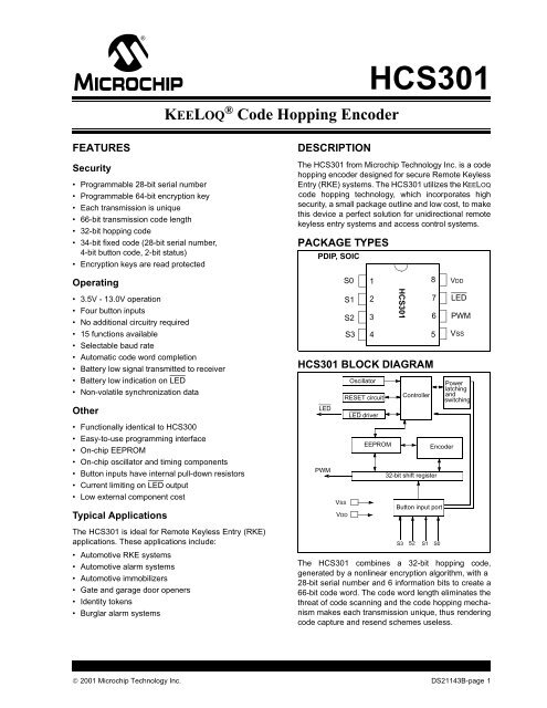
DESCRIPTION<br />
The <strong>HCS301</strong> from <strong>Microchip</strong> Technology Inc. is a code<br />
hopping encoder designed for secure Remote Keyless<br />
Entry (RKE) systems. The <strong>HCS301</strong> utilizes the <strong>KEELOQ</strong><br />
code hopping technology, which incorporates high<br />
security, a small package outline and low cost, to make<br />
this device a perfect solution for unidirectional remote<br />
keyless entry systems and access control systems.<br />
PACKAGE TYPES<br />
PDIP, SOIC<br />
<strong>HCS301</strong> BLOCK DIAGRAM<br />
LED<br />
PWM<br />
VSS<br />
VDD<br />
S0<br />
S1<br />
S2<br />
S3<br />
1<br />
2<br />
3<br />
4<br />
Oscillator<br />
RESET circuit<br />
LED driver<br />
EEPROM<br />
<strong>HCS301</strong><br />
Controller<br />
The <strong>HCS301</strong> combines a 32-bit hopping code,<br />
generated by a nonlinear encryption algorithm, with a<br />
28-bit serial number and 6 information bits to create a<br />
66-bit code word. The code word length eliminates the<br />
threat of code scanning and the code hopping mechanism<br />
makes each transmission unique, thus rendering<br />
code capture and resend schemes useless.<br />
8<br />
7<br />
6<br />
5<br />
32-bit shift register<br />
Button input port<br />
S3 S2 S1 S0<br />
<strong>Encoder</strong><br />
VDD<br />
LED<br />
PWM<br />
VSS<br />
Power<br />
latching<br />
and<br />
switching<br />
© 2001 <strong>Microchip</strong> Technology Inc. DS21143B-page 1
<strong>HCS301</strong><br />
The crypt key, serial number and configuration data are<br />
stored in an EEPROM array which is not accessible via<br />
any external connection. The EEPROM data is programmable<br />
but read-protected. The data can be verified<br />
only after an automatic erase and programming<br />
operation. This protects against attempts to gain<br />
access to keys or manipulate synchronization values.<br />
The <strong>HCS301</strong> provides an easy-to-use serial interface<br />
for programming the necessary keys, system parameters<br />
and configuration data.<br />
1.0 SYSTEM OVERVIEW<br />
Key Terms<br />
The following is a list of key terms used throughout this<br />
data sheet. For additional information on <strong>KEELOQ</strong> and<br />
<strong>Code</strong> <strong>Hopping</strong>, refer to Technical Brief 3 (TB003).<br />
• RKE - Remote Keyless Entry<br />
• Button Status - Indicates what button input(s)<br />
activated the transmission. Encompasses the 4<br />
button status bits S3, S2, S1 and S0 (Figure 4-2).<br />
• <strong>Code</strong> <strong>Hopping</strong> - A method by which a code,<br />
viewed externally to the system, appears to<br />
change unpredictably each time it is transmitted.<br />
• <strong>Code</strong> word - A block of data that is repeatedly<br />
transmitted upon button activation (Figure 4-1).<br />
• Transmission - A data stream consisting of<br />
repeating code words (Figure 8-2).<br />
• Crypt key - A unique and secret 64-bit number<br />
used to encrypt and decrypt data. In a symmetrical<br />
block cipher such as the <strong>KEELOQ</strong> algorithm,<br />
the encryption and decryption keys are equal and<br />
will therefore be referred to generally as the crypt<br />
key.<br />
• <strong>Encoder</strong> - A device that generates and encodes<br />
data.<br />
• Encryption Algorithm - A recipe whereby data is<br />
scrambled using a crypt key. The data can only be<br />
interpreted by the respective decryption algorithm<br />
using the same crypt key.<br />
• Decoder - A device that decodes data received<br />
from an encoder.<br />
• Decryption algorithm - A recipe whereby data<br />
scrambled by an encryption algorithm can be<br />
unscrambled using the same crypt key.<br />
• Learn – Learning involves the receiver calculating<br />
the transmitter’s appropriate crypt key, decrypting<br />
the received hopping code and storing the serial<br />
number, synchronization counter value and crypt<br />
key in EEPROM. The <strong>KEELOQ</strong> product family facilitates<br />
several learning strategies to be implemented<br />
on the decoder. The following are<br />
examples of what can be done.<br />
- Simple Learning<br />
The receiver uses a fixed crypt key, common<br />
to all components of all systems by the same<br />
manufacturer, to decrypt the received code<br />
word’s encrypted portion.<br />
- Normal Learning<br />
The receiver uses information transmitted<br />
during normal operation to derive the crypt<br />
key and decrypt the received code word’s<br />
encrypted portion.<br />
- Secure Learn<br />
The transmitter is activated through a special<br />
button combination to transmit a stored 60-bit<br />
seed value used to generate the transmitter’s<br />
crypt key. The receiver uses this seed value<br />
to derive the same crypt key and decrypt the<br />
received code word’s encrypted portion.<br />
• Manufacturer’s code – A unique and secret 64-<br />
bit number used to generate unique encoder crypt<br />
keys. Each encoder is programmed with a crypt<br />
key that is a function of the manufacturer’s code.<br />
Each decoder is programmed with the manufacturer<br />
code itself.<br />
The <strong>HCS301</strong> code hopping encoder is designed specifically<br />
for keyless entry systems; primarily vehicles and<br />
home garage door openers. The encoder portion of a<br />
keyless entry system is integrated into a transmitter,<br />
carried by the user and operated to gain access to a<br />
vehicle or restricted area. The <strong>HCS301</strong> is meant to be<br />
a cost-effective yet secure solution to such systems,<br />
requiring very few external components (Figure 2-1).<br />
Most low-end keyless entry transmitters are given a<br />
fixed identification code that is transmitted every time a<br />
button is pushed. The number of unique identification<br />
codes in a low-end system is usually a relatively small<br />
number. These shortcomings provide an opportunity<br />
for a sophisticated thief to create a device that ‘grabs’<br />
a transmission and retransmits it later, or a device that<br />
quickly ‘scans’ all possible identification codes until the<br />
correct one is found.<br />
The <strong>HCS301</strong>, on the other hand, employs the <strong>KEELOQ</strong><br />
code hopping technology coupled with a transmission<br />
length of 66 bits to virtually eliminate the use of code<br />
‘grabbing’ or code ‘scanning’. The high security level of<br />
the <strong>HCS301</strong> is based on the patented <strong>KEELOQ</strong> technology.<br />
A block cipher based on a block length of 32 bits<br />
and a key length of 64 bits is used. The algorithm<br />
obscures the information in such a way that even if the<br />
transmission information (before coding) differs by only<br />
one bit from that of the previous transmission, the next<br />
DS21143B-page 2<br />
© 2001 <strong>Microchip</strong> Technology Inc.
<strong>HCS301</strong><br />
coded transmission will be completely different. Statistically,<br />
if only one bit in the 32-bit string of information<br />
changes, greater than 50 percent of the coded transmission<br />
bits will change.<br />
As indicated in the block diagram on page one, the<br />
<strong>HCS301</strong> has a small EEPROM array which must be<br />
loaded with several parameters before use; most often<br />
programmed by the manufacturer at the time of production.<br />
The most important of these are:<br />
• A 28-bit serial number, typically unique for every<br />
encoder<br />
• A crypt key<br />
• An initial 16-bit synchronization value<br />
• A 16-bit configuration value<br />
The crypt key generation typically inputs the transmitter<br />
serial number and 64-bit manufacturer’s code into the<br />
key generation algorithm (Figure 1-1). The manufacturer’s<br />
code is chosen by the system manufacturer and<br />
must be carefully controlled as it is a pivotal part of the<br />
overall system security.<br />
FIGURE 1-1:<br />
CREATION AND STORAGE OF CRYPT KEY DURING PRODUCTION<br />
Production<br />
Programmer<br />
Manufacturer’s<br />
<strong>Code</strong><br />
Transmitter<br />
Serial Number<br />
Key<br />
Generation<br />
Algorithm<br />
Crypt<br />
Key<br />
<strong>HCS301</strong><br />
EEPROM Array<br />
Serial Number<br />
Crypt Key<br />
Sync Counter<br />
.<br />
.<br />
.<br />
The 16-bit synchronization counter is the basis behind<br />
the transmitted code word changing for each transmission;<br />
it increments each time a button is pressed. Due<br />
to the code hopping algorithm’s complexity, each increment<br />
of the synchronization value results in greater<br />
than 50% of the bits changing in the transmitted code<br />
word.<br />
Figure 1-2 shows how the key values in EEPROM are<br />
used in the encoder. Once the encoder detects a button<br />
press, it reads the button inputs and updates the synchronization<br />
counter. The synchronization counter and<br />
crypt key are input to the encryption algorithm and the<br />
output is 32 bits of encrypted information. This data will<br />
change with every button press, its value appearing<br />
externally to ‘randomly hop around’, hence it is referred<br />
to as the hopping portion of the code word. The 32-bit<br />
hopping code is combined with the button information<br />
and serial number to form the code word transmitted to<br />
the receiver. The code word format is explained in<br />
greater detail in Section 4.0.<br />
A receiver may use any type of controller as a decoder,<br />
but it is typically a microcontroller with compatible firmware<br />
that allows the decoder to operate in conjunction<br />
with an <strong>HCS301</strong> based transmitter. Section 7.0<br />
provides detail on integrating the <strong>HCS301</strong> into a system.<br />
A transmitter must first be ‘learned’ by the receiver<br />
before its use is allowed in the system. Learning<br />
includes calculating the transmitter’s appropriate crypt<br />
key, decrypting the received hopping code and storing<br />
the serial number, synchronization counter value and<br />
crypt key in EEPROM.<br />
In normal operation, each received message of valid<br />
format is evaluated. The serial number is used to determine<br />
if it is from a learned transmitter. If from a learned<br />
transmitter, the message is decrypted and the synchronization<br />
counter is verified. Finally, the button status is<br />
checked to see what operation is requested. Figure 1-3<br />
shows the relationship between some of the values<br />
stored by the receiver and the values received from<br />
the transmitter.<br />
© 2001 <strong>Microchip</strong> Technology Inc. DS21143B-page 3
<strong>HCS301</strong><br />
FIGURE 1-2:<br />
BUILDING THE TRANSMITTED CODE WORD (ENCODER)<br />
EEPROM Array<br />
Crypt Key<br />
Sync Counter<br />
<strong>KEELOQ</strong><br />
Encryption<br />
Algorithm<br />
Serial Number<br />
Button Press<br />
Information<br />
Serial Number<br />
32 Bits<br />
Encrypted <strong>Data</strong><br />
Transmitted Information<br />
FIGURE 1-3:<br />
BASIC OPERATION OF RECEIVER (DECODER)<br />
1<br />
Received Information<br />
EEPROM Array<br />
Button Press<br />
Information<br />
Serial Number<br />
32 Bits of<br />
Encrypted <strong>Data</strong><br />
Manufacturer <strong>Code</strong><br />
2<br />
Check for<br />
Match<br />
Serial Number<br />
Sync Counter<br />
Crypt Key<br />
3<br />
<strong>KEELOQ</strong><br />
Decryption<br />
Algorithm<br />
Perform Function<br />
5<br />
Indicated by<br />
button press<br />
Decrypted<br />
Synchronization<br />
Counter<br />
4<br />
Check for<br />
Match<br />
NOTE: Circled numbers indicate the order of execution.<br />
DS21143B-page 4<br />
© 2001 <strong>Microchip</strong> Technology Inc.
<strong>HCS301</strong><br />
2.0 DEVICE OPERATION<br />
TABLE 2-1:<br />
PIN DESCRIPTIONS<br />
As shown in the typical application circuits (Figure 2-1),<br />
the <strong>HCS301</strong> is a simple device to use. It requires only<br />
the addition of buttons and RF circuitry for use as the<br />
transmitter in your security application. A description of<br />
each pin is given in Table 2-1.<br />
Note:<br />
FIGURE 2-1:<br />
When VDD > 9.0V and driving low capacitive<br />
loads, a resistor with a minimum value<br />
of 50Ω should be used in line with VDD.<br />
This prevents clamping of PWM at 9.0V in<br />
the event of PWM overshoot.<br />
B0<br />
B1<br />
+12V<br />
(2)<br />
R<br />
TYPICAL CIRCUITS<br />
S0<br />
S1<br />
S2<br />
S3<br />
2 button remote control<br />
B4 B3 B2 B1 B0<br />
S0<br />
S1<br />
S2<br />
S3<br />
5 button remote control (1)<br />
VDD<br />
LED<br />
PWM<br />
VSS<br />
VDD<br />
LED<br />
PWM<br />
VSS<br />
+12V<br />
(2)<br />
R<br />
Tx out<br />
Tx out<br />
Note 1: Up to 15 functions can be implemented by pressing<br />
more than one button simultaneously or by using a<br />
suitable diode array.<br />
Name<br />
Pin<br />
Number<br />
Description<br />
S0 1 Switch input 0<br />
S1 2 Switch input 1<br />
S2 3 Switch input 2 / Clock pin when in<br />
Programming mode<br />
S3 4 Switch input 3<br />
VSS 5 Ground reference<br />
PWM 6 Pulse Width Modulation (PWM)<br />
output pin / <strong>Data</strong> pin for<br />
Programming mode<br />
LED 7 Cathode connection for LED<br />
VDD 8 Positive supply voltage<br />
The <strong>HCS301</strong> will wake-up upon detecting a button<br />
press and delay approximately 10 ms for button<br />
debounce (Figure 2-2). The synchronization counter,<br />
discrimination value and button information will be<br />
encrypted to form the hopping code. The hopping code<br />
portion will change every transmission, even if the<br />
same button is pushed again. A code word that has<br />
been transmitted will not repeat for more than 64K<br />
transmissions. This provides more than 18 years of use<br />
before a code is repeated; based on 10 operations per<br />
day. Overflow information sent from the encoder can be<br />
used to extend the number of unique transmissions to<br />
more than 192K.<br />
If in the transmit process it is detected that a new button(s)<br />
has been pressed, a RESET will immediately<br />
occur and the current code word will not be completed.<br />
Please note that buttons removed will not have any<br />
effect on the code word unless no buttons remain<br />
pressed; in which case the code word will be completed<br />
and the power-down will occur.<br />
2: Resistor R is recommended for current limiting.<br />
© 2001 <strong>Microchip</strong> Technology Inc. DS21143B-page 5
<strong>HCS301</strong><br />
FIGURE 2-2: ENCODER OPERATION 3.0 EEPROM MEMORY<br />
ORGANIZATION<br />
Power-Up<br />
(A button has been pressed)<br />
RESET and Debounce Delay<br />
(10 ms)<br />
Sample Inputs<br />
The <strong>HCS301</strong> contains 192 bits (12 x 16-bit words) of<br />
EEPROM memory (Table 3-1). This EEPROM array is<br />
used to store the encryption key information,<br />
synchronization value, etc. Further descriptions of the<br />
memory array is given in the following sections.<br />
Yes<br />
Update Sync Info<br />
Encrypt With<br />
Crypt Key<br />
Load Transmit Register<br />
Transmit<br />
Buttons<br />
Added<br />
?<br />
No<br />
All<br />
Buttons<br />
Released<br />
?<br />
Yes<br />
Complete <strong>Code</strong><br />
Word Transmission<br />
Stop<br />
No<br />
TABLE 3-1:<br />
EEPROM MEMORY MAP<br />
WORD<br />
ADDRESS<br />
MNEMONIC DESCRIPTION<br />
0 KEY_0 64-bit encryption key<br />
(word 0) LSb’s<br />
1 KEY_1 64-bit encryption key<br />
(word 1)<br />
2 KEY_2 64-bit encryption key<br />
(word 2)<br />
3 KEY_3 64-bit encryption key<br />
(word 3) MSb’s<br />
4 SYNC 16-bit synchronization<br />
value<br />
5 RESERVED Set to 0000H<br />
6 SER_0 Device Serial Number<br />
(word 0) LSb’s<br />
7 SER_1(Note) Device Serial Number<br />
(word 1) MSb’s<br />
8 SEED_0 Seed Value (word 0)<br />
9 SEED_1 Seed Value (word 1)<br />
10 RESERVED Set to 0000H<br />
11 CONFIG Config Word<br />
Note:<br />
The MSB of the serial number contains a bit<br />
used to select the Auto-shutoff timer.<br />
3.1 KEY_0 - KEY_3 (64-Bit Crypt Key)<br />
The 64-bit crypt key is used to create the encrypted<br />
message transmitted to the receiver. This key is calculated<br />
and programmed during production using a key<br />
generation algorithm. The key generation algorithm<br />
may be different from the <strong>KEELOQ</strong> algorithm. Inputs to<br />
the key generation algorithm are typically the transmitter’s<br />
serial number and the 64-bit manufacturer’s code.<br />
While the key generation algorithm supplied from<br />
<strong>Microchip</strong> is the typical method used, a user may elect<br />
to create their own method of key generation. This may<br />
be done providing that the decoder is programmed with<br />
the same means of creating the key for<br />
decryption purposes.<br />
DS21143B-page 6<br />
© 2001 <strong>Microchip</strong> Technology Inc.
<strong>HCS301</strong><br />
3.2 SYNC (Synchronization Counter)<br />
This is the 16-bit synchronization value that is used to<br />
create the hopping code for transmission. This value<br />
will increment after every transmission.<br />
3.3 Reserved<br />
Must be initialized to 0000H.<br />
3.4 SER_0, SER_1<br />
(<strong>Encoder</strong> Serial Number)<br />
SER_0 and SER_1 are the lower and upper words of<br />
the device serial number, respectively. Although there<br />
are 32 bits allocated for the serial number, only the<br />
lower order 28 bits are transmitted. The serial number<br />
is meant to be unique for every transmitter.<br />
3.4.1 AUTO-SHUTOFF TIMER ENABLE<br />
The Most Significant bit of the serial number (Bit 31) is<br />
used to turn the Auto-shutoff timer on or off. This timer<br />
prevents the transmitter from draining the battery<br />
should a button get stuck in the on position for a long<br />
period of time. The time period is approximately<br />
25 seconds, after which the device will go to the Timeout<br />
mode. When in the Time-out mode, the device will<br />
stop transmitting, although since some circuits within<br />
the device are still active, the current draw within the<br />
Shutoff mode will be higher than Standby mode. If the<br />
Most Significant bit in the serial number is a one, then<br />
the Auto-shutoff timer is enabled, and a zero in the<br />
Most Significant bit will disable the timer. The length of<br />
the timer is not selectable.<br />
3.5 SEED_0, SEED_1 (Seed Word)<br />
The 2-word (32-bit) seed code will be transmitted when<br />
all three buttons are pressed at the same time (see<br />
Figure 4-2). This allows the system designer to implement<br />
the secure learn feature or use this fixed code<br />
word as part of a different key generation/tracking process.<br />
3.6 CONFIG (Configuration Word)<br />
The Configuration Word is a 16-bit word stored in<br />
EEPROM array that is used by the device to store<br />
information used during the encryption process, as well<br />
as the status of option configurations. The following<br />
sections further explain these bits.<br />
TABLE 3-2:<br />
CONFIGURATION WORD<br />
Bit Number<br />
Bit Description<br />
0 Discrimination Bit 0<br />
1 Discrimination Bit 1<br />
2 Discrimination Bit 2<br />
3 Discrimination Bit 3<br />
4 Discrimination Bit 4<br />
5 Discrimination Bit 5<br />
6 Discrimination Bit 6<br />
7 Discrimination Bit 7<br />
8 Discrimination Bit 8<br />
9 Discrimination Bit 9<br />
10 Overflow Bit 0 (OVR0)<br />
11 Overflow Bit 1 (OVR1)<br />
12 Low Voltage Trip Point Select<br />
(VLOW SEL)<br />
13 Baud rate Select Bit 0 (BSL0)<br />
14 Baud rate Select Bit 1 (BSL1)<br />
15 Reserved, set to 0<br />
3.6.1 DISCRIMINATION VALUE<br />
(DISC0 TO DISC9)<br />
The discrimination value aids the post-decryption<br />
check on the decoder end. It may be any value, but in<br />
a typical system it will be programmed as the 10 Least<br />
Significant bits of the serial number. Values other than<br />
this must be separately stored by the receiver when a<br />
transmitter is learned. The discrimination bits are part<br />
of the information that form the encrypted portion of the<br />
transmission (Figure 4-2). After the receiver has<br />
decrypted a transmission, the discrimination bits are<br />
checked against the receiver’s stored value to verify<br />
that the decryption process was valid. If the discrimination<br />
value was programmed as the 10 LSb’s of the<br />
serial number then it may merely be compared to the<br />
respective bits of the received serial number; saving<br />
EEPROM space.<br />
3.6.2 OVERFLOW BITS<br />
(OVR0, OVR1)<br />
The overflow bits are used to extend the number of<br />
possible synchronization values. The synchronization<br />
counter is 16 bits in length, yielding 65,536 values<br />
before the cycle repeats. Under typical use of<br />
10 operations a day, this will provide nearly 18 years of<br />
use before a repeated value will be used. Should the<br />
system designer conclude that is not adequate, then<br />
the overflow bits can be utilized to extend the number<br />
© 2001 <strong>Microchip</strong> Technology Inc. DS21143B-page 7
<strong>HCS301</strong><br />
of unique values. This can be done by programming<br />
OVR0 and OVR1 to 1s at the time of production. The<br />
encoder will automatically clear OVR0 the first time that<br />
the synchronization value wraps from 0xFFFF to<br />
0x0000 and clear OVR1 the second time the counter<br />
wraps. Once cleared, OVR0 and OVR1 cannot be set<br />
again, thereby creating a permanent record of the<br />
counter overflow. This prevents fast cycling of 64K<br />
counter. If the decoder system is programmed to track<br />
the overflow bits, then the effective number of unique<br />
synchronization values can be extended to 196,608.<br />
3.6.4 LOW VOLTAGE TRIP POINT<br />
SELECT<br />
The low voltage trip point select bit is used to tell the<br />
<strong>HCS301</strong> what VDD level is being used. This information<br />
will be used by the device to determine when to send the<br />
voltage low signal to the receiver. When this bit is set to<br />
a one, the VDD level is assumed to be operating from a<br />
9V or 12V VDD level. If the bit is set low, then the VDD level<br />
is assumed to be 6.0 volts. Refer to Figure 3-1 for voltage<br />
trip point.<br />
3.6.3 BAUD RATE SELECT BITS<br />
(BSL0, BSL1)<br />
BSL0 and BSL1 select the speed of transmission and<br />
the code word blanking. Table 3-3 shows how the bits<br />
are used to select the different baud rates and<br />
Section 5.7 provides detailed explanation in code word<br />
blanking.<br />
TABLE 3-3:<br />
BSL1<br />
BSL0<br />
BAUD RATE SELECT<br />
Basic Pulse<br />
Element<br />
<strong>Code</strong> Words<br />
Transmitted<br />
0 0 400 µs All<br />
0 1 200 µs 1 out of 2<br />
1 0 100 µs 1 out of 2<br />
1 1 100 µs 1 out of 4<br />
FIGURE 3-1:<br />
Volts (V)<br />
5.5<br />
5.0<br />
4.5<br />
4.0<br />
3.5<br />
3.0<br />
2.5<br />
9.0<br />
8.5<br />
8.0<br />
7.5<br />
7.0<br />
VOLTAGE TRIP POINTS<br />
BY CHARACTERIZATION<br />
VLOW sel = 0<br />
VLOW sel = 1<br />
VLOW<br />
Max<br />
Min<br />
Max<br />
Min<br />
-40 -20 0 20 40 60 80 100<br />
Temp (C)<br />
DS21143B-page 8<br />
© 2001 <strong>Microchip</strong> Technology Inc.
<strong>HCS301</strong><br />
4.0 TRANSMITTED WORD<br />
4.1 <strong>Code</strong> Word Format<br />
The <strong>HCS301</strong> code word is made up of several parts<br />
(Figure 4-1). Each code word contains a 50% duty<br />
cycle preamble, a header, 32 bits of encrypted data and<br />
34 bits of fixed data followed by a guard period before<br />
another code word can begin. Refer to Table 8-4 for<br />
code word timing.<br />
4.2 <strong>Code</strong> Word Organization<br />
The <strong>HCS301</strong> transmits a 66-bit code word when a<br />
button is pressed. The 66-bit word is constructed from<br />
a Fixed <strong>Code</strong> portion and an Encrypted <strong>Code</strong> portion<br />
(Figure 4-2).<br />
The 32 bits of Encrypted <strong>Data</strong> are generated from 4<br />
button bits, 12 discrimination bits and the 16-bit sync<br />
value. The encrypted portion alone provides up to four<br />
billion changing code combinations.<br />
The 34 bits of Fixed <strong>Code</strong> <strong>Data</strong> are made up of 2 status<br />
bits, 4 button bits and the 28-bit serial number. The<br />
fixed and encrypted sections combined increase the<br />
number of code combinations to 7.38 x 10 19 .<br />
FIGURE 4-1:<br />
CODE WORD FORMAT<br />
TE<br />
TE<br />
TE<br />
LOGIC ‘0’<br />
LOGIC ‘1’<br />
Bit<br />
Period<br />
50% Duty Cycle<br />
Encrypted Portion Fixed Portion of Guard<br />
Preamble Header of Transmission Transmission Time<br />
TP TH THOP TFIX TG<br />
FIGURE 4-2:<br />
CODE WORD ORGANIZATION<br />
34 bits of Fixed Portion 32 bits of Encrypted Portion<br />
MSb<br />
Repeat<br />
(1 bit)<br />
VLOW<br />
(1 bit)<br />
Button<br />
Status<br />
S2 S1 S0 S3<br />
Serial Number<br />
(28 bits)<br />
Button<br />
Status<br />
S2 S1 S0 S3<br />
OVR<br />
(2 bits)<br />
DISC<br />
(10 bits)<br />
Sync Counter<br />
(16 bits)<br />
66 <strong>Data</strong> bits<br />
Transmitted<br />
LSb first.<br />
LSb<br />
MSb<br />
Repeat<br />
(1 bit)<br />
VLOW<br />
(1 bit)<br />
Button<br />
Status<br />
1 1 1 1<br />
Serial Number<br />
(28 bits)<br />
SEED<br />
(32 bits)<br />
Note: SEED replaces Encrypted Portion when all button inputs are activated at the same time.<br />
LSb<br />
© 2001 <strong>Microchip</strong> Technology Inc. DS21143B-page 9
<strong>HCS301</strong><br />
4.3 Synchronous Transmission Mode<br />
Synchronous Transmission mode can be used to clock<br />
the code word out using an external clock.<br />
To enter Synchronous Transmission mode, the Programming<br />
mode start-up sequence must be executed<br />
as shown in Figure 4-3. If either S1 or S0 is set on the<br />
falling edge of S2 (or S3), the device enters Synchronous<br />
Transmission mode. In this mode, it functions as<br />
a normal transmitter, with the exception that the timing<br />
of the PWM data string is controlled externally and 16<br />
extra bits are transmitted at the end with the code word.<br />
The button code will be the S0, S1 value at the falling<br />
edge of S2 or S3. The timing of the PWM data string is<br />
controlled by supplying a clock on S2 or S3 and should<br />
not exceed 20 kHz. The code word is the same as in<br />
PWM mode with 16 reserved bits at the end of the<br />
word. The reserved bits can be ignored. When in Synchronous<br />
Transmission mode S2 or S3 should not be<br />
toggled until all internal processing has been completed<br />
as shown in Figure 4-4.<br />
FIGURE 4-3:<br />
SYNCHRONOUS TRANSMISSION MODE<br />
TPS TPH1 TPH2 t = 50ms Preamble Header <strong>Data</strong><br />
PWM<br />
S2<br />
S[1:0]<br />
“01,10,11”<br />
FIGURE 4-4:<br />
CODE WORD ORGANIZATION (SYNCHRONOUS TRANSMISSION MODE)<br />
Fixed Portion<br />
Encrypted Portion<br />
MSb<br />
Reserved<br />
(16 bits)<br />
Padding<br />
(2 bits)<br />
Button<br />
Status<br />
S2 S1 S0 S3<br />
Serial Number<br />
(28 bits)<br />
Button<br />
Status<br />
S2 S1 S0 S3<br />
DISC+ OVR<br />
(12 bits)<br />
82 <strong>Data</strong> bits<br />
Transmitted<br />
LSb first.<br />
Sync Counter<br />
(16 bits)<br />
LSb<br />
DS21143B-page 10<br />
© 2001 <strong>Microchip</strong> Technology Inc.
<strong>HCS301</strong><br />
5.0 SPECIAL FEATURES<br />
5.1 <strong>Code</strong> Word Completion<br />
The code word completion feature ensures that entire<br />
code words are transmitted, even if the button is<br />
released before the code word is complete. If the button<br />
is held down beyond the time for one code word,<br />
multiple code words will result. If another button is activated<br />
during a transmission, the active transmission<br />
will be aborted and a new transmission will begin using<br />
the new button information.<br />
5.2 LED Output Operation<br />
During normal transmission the LED output is LOW. If<br />
the supply voltage drops below the low voltage trip<br />
point, the LED output will be toggled at approximately<br />
5Hz during the transmission (Section 3.6.4).<br />
5.3 RPT: Repeat Indicator<br />
This bit will be low for the first transmitted word. If a<br />
button is held down for more than one transmitted code<br />
word, this bit will be set to indicate a repeated code<br />
word and remain set until the button is released.<br />
5.6 Seed Transmission<br />
In order to increase the level of security in a system, it<br />
is possible for the receiver to implement what is known<br />
as a secure learn function. This can be done by utilizing<br />
the seed value stored in EEPROM, transmitted only<br />
when all three button inputs are pressed at the same<br />
time (Table 5-1). Instead of the normal key generation<br />
inputs being used to create the crypt key, this seed<br />
value is used.<br />
TABLE 5-1:<br />
PIN ACTIVATION TABLE<br />
Function S3 S2 S1 S0<br />
Standby 0 0 0 0 0<br />
1 0 0 0 1<br />
<strong>Hopping</strong> <strong>Code</strong><br />
2 0 0 1 0<br />
- - - - -<br />
13 1 1 0 1<br />
14 1 1 1 0<br />
Seed <strong>Code</strong> 15 1 1 1 1<br />
5.4 VLOW: Voltage LOW Indicator<br />
The VLOW signal is transmitted so the receiver can give<br />
an indication to the user that the transmitter battery is<br />
low. The VLOW bit is included in every transmission<br />
(Figure 4-2 and Figure 8-5) and will be transmitted as a<br />
zero if the operating voltage is above the low voltage<br />
trip point. Refer to Figure 4-2. The trip point is selectable<br />
based on the battery voltage being used. See Section<br />
3.6.3 for a description of how the low voltage trip<br />
point is configured.<br />
5.5 Auto-shutoff<br />
The Auto-shutoff function automatically stops the<br />
device from transmitting if a button inadvertently gets<br />
pressed for a long period of time. This will prevent the<br />
device from draining the battery if a button gets<br />
pressed while the transmitter is in a pocket or purse.<br />
This function can be enabled or disabled and is<br />
selected by setting or clearing the Auto-shutoff bit (see<br />
Section 3.4.1). Setting this bit high will enable the function<br />
(turn Auto-shutoff function on) and setting the bit<br />
low will disable the function. Time-out period is approximately<br />
25 seconds.<br />
© 2001 <strong>Microchip</strong> Technology Inc. DS21143B-page 11
<strong>HCS301</strong><br />
5.7 Blank Alternate <strong>Code</strong> Word<br />
Federal Communications Commission (FCC) part 15<br />
rules specify the limits on worst case average fundamental<br />
power and harmonics that can be transmitted in<br />
a 100 ms window. For FCC approval purposes, it may<br />
therefore be advantageous to minimize the transmission<br />
duty cycle. This can be achieved by minimizing the<br />
duty cycle of the individual bits as well as by blanking<br />
out consecutive code words. Blank Alternate <strong>Code</strong><br />
Word (BACW) may be used to reduce the average<br />
power of a transmission by transmitting only every second<br />
code word (Figure 5-1). This is a selectable feature<br />
that is determined in conjunction with the baud rate<br />
selection bit BSL0.<br />
Enabling the BACW option may likewise allow the user<br />
to transmit a higher amplitude transmission as the time<br />
averaged power is reduced. BACW effectively halves<br />
the RF on time for a given transmission so the RF output<br />
power could theoretically be doubled while maintaining<br />
the same time averaged output power.<br />
FIGURE 5-1:<br />
BLANK ALTERNATE CODE WORD (BACW)<br />
Amplitude<br />
BACW Disabled<br />
(All words transmitted)<br />
A<br />
<strong>Code</strong> Word<br />
<strong>Code</strong> Word <strong>Code</strong> Word <strong>Code</strong> Word<br />
BACW Enabled<br />
(1 out of 2 transmitted)<br />
2A<br />
BACW Enabled<br />
(1 out of 4 transmitted)<br />
4A<br />
Time<br />
DS21143B-page 12<br />
© 2001 <strong>Microchip</strong> Technology Inc.
<strong>HCS301</strong><br />
6.0 PROGRAMMING THE <strong>HCS301</strong><br />
When using the <strong>HCS301</strong> in a system, the user will have<br />
to program some parameters into the device including<br />
the serial number and the secret key before it can be<br />
used. The programming cycle allows the user to input<br />
all 192 bits in a serial data stream, which are then<br />
stored internally in EEPROM. Programming will be<br />
initiated by forcing the PWM line high, after the S2 (or<br />
S3) line has been held high for the appropriate length<br />
of time line (Table 6-1 and Figure 6-1). After the Program<br />
mode is entered, a delay must be provided to the<br />
device for the automatic bulk write cycle to complete.<br />
This will set all locations in the EEPROM to zeros. The<br />
device can then be programmed by clocking in 16 bits<br />
at a time, using S2 (or S3) as the clock line and PWM<br />
as the data in line. After each 16-bit word is loaded, a<br />
programming delay is required for the internal program<br />
cycle to complete. This delay can take up to TWC. At the<br />
end of the programming cycle, the device can be verified<br />
(Figure 6-2) by reading back the EEPROM. Reading<br />
is done by clocking the S2 (or S3) line and reading<br />
the data bits on PWM. For security reasons, it is not<br />
possible to execute a verify function without first programming<br />
the EEPROM. A Verify operation can only<br />
be done once, immediately following the Program<br />
cycle.<br />
Note:<br />
To ensure that the device does not accidentally<br />
enter Programming mode, PWM<br />
should never be pulled high by the circuit<br />
connected to it. Special care should be<br />
taken when driving PNP RF transistors.<br />
FIGURE 6-1: PROGRAMMING WAVEFORMS<br />
Enter Program<br />
Mode TPBW<br />
TCLKH<br />
TDS<br />
TWC<br />
S2 (S3)<br />
(Clock)<br />
PWM<br />
(<strong>Data</strong>)<br />
TPS<br />
TPH1<br />
TCLKL TDH<br />
Bit 0 Bit 1 Bit 2 Bit 3 Bit 14 Bit 15 Bit 16 Bit 17<br />
TPH2<br />
<strong>Data</strong> for Word 0 (KEY_0) <strong>Data</strong> for Word 1<br />
Repeat for each word (12 times)<br />
Note 1: Unused button inputs to be held to ground during the entire programming sequence.<br />
2: The VDD pin must be taken to ground after a Program/Verify cycle.<br />
FIGURE 6-2:<br />
VERIFY WAVEFORMS<br />
End of Programming Cycle<br />
Beginning of Verify Cycle<br />
<strong>Data</strong> from Word 0<br />
PWM<br />
(<strong>Data</strong>)<br />
S2 (S3)<br />
(Clock)<br />
Bit190 Bit191<br />
TWC<br />
Bit 0<br />
Bit 1 Bit 2 Bit 3 Bit 14 Bit 15 Bit 16 Bit 17 Bit190 Bit191<br />
TDV<br />
Note: If a Verify operation is to be done, then it must immediately follow the Program cycle.<br />
© 2001 <strong>Microchip</strong> Technology Inc. DS21143B-page 13
<strong>HCS301</strong><br />
TABLE 6-1:<br />
PROGRAMMING/VERIFY TIMING REQUIREMENTS<br />
VDD = 5.0V ± 10%, 25 °C ± 5 °C<br />
Parameter Symbol Min. Max. Units<br />
Program mode setup time TPS 3.5 4.5 ms<br />
Hold time 1 TPH1 3.5 — ms<br />
Hold time 2 TPH2 50 — µs<br />
Bulk Write time TPBW 4.0 — ms<br />
Program delay time TPROG 4.0 — ms<br />
Program cycle time TWC 50 — ms<br />
Clock low time TCLKL 50 — µs<br />
Clock high time TCLKH 50 — µs<br />
<strong>Data</strong> setup time TDS 0 — µs (1)<br />
<strong>Data</strong> hold time TDH 30 — µs (1)<br />
<strong>Data</strong> out valid time TDV — 30 µs (1)<br />
Note 1: Typical values - not tested in production.<br />
DS21143B-page 14<br />
© 2001 <strong>Microchip</strong> Technology Inc.
<strong>HCS301</strong><br />
7.0 INTEGRATING THE <strong>HCS301</strong><br />
INTO A SYSTEM<br />
Use of the <strong>HCS301</strong> in a system requires a compatible<br />
decoder. This decoder is typically a microcontroller with<br />
compatible firmware. <strong>Microchip</strong> will provide (via a<br />
license agreement) firmware routines that accept<br />
transmissions from the <strong>HCS301</strong> and decrypt the<br />
hopping code portion of the data stream. These<br />
routines provide system designers the means to<br />
develop their own decoding system.<br />
7.1 Learning a Transmitter to a<br />
Receiver<br />
A transmitter must first be ’learned’ by a decoder before<br />
its use is allowed in the system. Several learning strategies<br />
are possible, Figure 7-1 details a typical learn<br />
sequence. Core to each, the decoder must minimally<br />
store each learned transmitter’s serial number and current<br />
synchronization counter value in EEPROM. Additionally,<br />
the decoder typically stores each transmitter’s<br />
unique crypt key. The maximum number of learned<br />
transmitters will therefore be relative to the available<br />
EEPROM.<br />
A transmitter’s serial number is transmitted in the clear<br />
but the synchronization counter only exists in the code<br />
word’s encrypted portion. The decoder obtains the<br />
counter value by decrypting using the same key used<br />
to encrypt the information. The <strong>KEELOQ</strong> algorithm is a<br />
symmetrical block cipher so the encryption and decryption<br />
keys are identical and referred to generally as the<br />
crypt key. The encoder receives its crypt key during<br />
manufacturing. The decoder is programmed with the<br />
ability to generate a crypt key as well as all but one<br />
required input to the key generation routine; typically<br />
the transmitter’s serial number.<br />
Figure 7-1 summarizes a typical learn sequence. The<br />
decoder receives and authenticates a first transmission;<br />
first button press. Authentication involves generating<br />
the appropriate crypt key, decrypting, validating<br />
the correct key usage via the discrimination bits and<br />
buffering the counter value. A second transmission is<br />
received and authenticated. A final check verifies the<br />
counter values were sequential; consecutive button<br />
presses. If the learn sequence is successfully complete,<br />
the decoder stores the learned transmitter’s<br />
serial number, current synchronization counter value<br />
and appropriate crypt key. From now on the crypt key<br />
will be retrieved from EEPROM during normal operation<br />
instead of recalculating it for each transmission<br />
received.<br />
Certain learning strategies have been patented and<br />
care must be taken not to infringe.<br />
FIGURE 7-1:<br />
Enter Learn<br />
Mode<br />
Wait for Reception<br />
of a Valid <strong>Code</strong><br />
Generate Key<br />
from Serial Number<br />
Use Generated Key<br />
to Decrypt<br />
Compare Discrimination<br />
Value with Fixed Value<br />
Equal<br />
?<br />
Yes<br />
Wait for Reception<br />
of Second Valid <strong>Code</strong><br />
Use Generated Key<br />
to Decrypt<br />
Compare Discrimination<br />
Value with Fixed Value<br />
Equal<br />
?<br />
Counters<br />
Sequential<br />
?<br />
Yes<br />
Learn successful Store:<br />
Serial number<br />
Encryption key<br />
Synchronization counter<br />
Exit<br />
Yes<br />
TYPICAL LEARN<br />
SEQUENCE<br />
No<br />
No<br />
No<br />
Learn<br />
Unsuccessful<br />
© 2001 <strong>Microchip</strong> Technology Inc. DS21143B-page 15
<strong>HCS301</strong><br />
7.2 Decoder Operation<br />
Figure 7-2 summarizes normal decoder operation. The<br />
decoder waits until a transmission is received. The<br />
received serial number is compared to the EEPROM<br />
table of learned transmitters to first determine if this<br />
transmitter’s use is allowed in the system. If from a<br />
learned transmitter, the transmission is decrypted<br />
using the stored crypt key and authenticated via the<br />
discrimination bits for appropriate crypt key usage. If<br />
the decryption was valid the synchronization value is<br />
evaluated.<br />
FIGURE 7-2:<br />
No<br />
Transmission<br />
Received<br />
?<br />
Does<br />
No Serial Number<br />
Match<br />
?<br />
Yes<br />
Decrypt Transmission<br />
No<br />
No<br />
No<br />
Start<br />
Is<br />
Decryption<br />
Valid<br />
?<br />
Is<br />
Counter<br />
Within 16<br />
?<br />
Is<br />
Counter<br />
Within 32K<br />
?<br />
Yes<br />
Save Counter<br />
in Temp Location<br />
TYPICAL DECODER<br />
OPERATION<br />
Yes<br />
Yes<br />
No<br />
Yes<br />
Execute<br />
Command<br />
and<br />
Update<br />
Counter<br />
7.3 Synchronization with Decoder<br />
(Evaluating the Counter)<br />
The <strong>KEELOQ</strong> technology patent scope includes a<br />
sophisticated synchronization technique that does not<br />
require the calculation and storage of future codes. The<br />
technique securely blocks invalid transmissions while<br />
providing transparent resynchronization to transmitters<br />
inadvertently activated away from the receiver.<br />
Figure 7-3 shows a 3-partition, rotating synchronization<br />
window. The size of each window is optional but the<br />
technique is fundamental. Each time a transmission is<br />
authenticated, the intended function is executed and<br />
the transmission’s synchronization counter value is<br />
stored in EEPROM. From the currently stored counter<br />
value there is an initial "Single Operation" forward window<br />
of 16 codes. If the difference between a received<br />
synchronization counter and the last stored counter is<br />
within 16, the intended function will be executed on the<br />
single button press and the new synchronization<br />
counter will be stored. Storing the new synchronization<br />
counter value effectively rotates the entire synchronization<br />
window.<br />
A "Double Operation" (resynchronization) window further<br />
exists from the Single Operation window up to 32K<br />
codes forward of the currently stored counter value. It<br />
is referred to as "Double Operation" because a transmission<br />
with synchronization counter value in this window<br />
will require an additional, sequential counter<br />
transmission prior to executing the intended function.<br />
Upon receiving the sequential transmission the<br />
decoder executes the intended function and stores the<br />
synchronization counter value. This resynchronization<br />
occurs transparently to the user as it is human nature<br />
to press the button a second time if the first was unsuccessful.<br />
The third window is a "Blocked Window" ranging from<br />
the double operation window to the currently stored<br />
synchronization counter value. Any transmission with<br />
synchronization counter value within this window will<br />
be ignored. This window excludes previously used,<br />
perhaps code-grabbed transmissions from accessing<br />
the system.<br />
Note:<br />
The synchronization method described in<br />
this section is only a typical implementation<br />
and because it is usually implemented in<br />
firmware, it can be altered to fit the needs<br />
of a particular system.<br />
DS21143B-page 16<br />
© 2001 <strong>Microchip</strong> Technology Inc.
<strong>HCS301</strong><br />
FIGURE 7-3:<br />
SYNCHRONIZATION WINDOW<br />
Entire Window<br />
rotates to eliminate<br />
use of previously<br />
used codes<br />
Blocked<br />
Window<br />
(32K <strong>Code</strong>s)<br />
Double Operation<br />
(resynchronization)<br />
Window<br />
(32K <strong>Code</strong>s)<br />
Stored<br />
Synchronization<br />
Counter Value<br />
Single Operation<br />
Window<br />
(16 <strong>Code</strong>s)<br />
© 2001 <strong>Microchip</strong> Technology Inc. DS21143B-page 17
<strong>HCS301</strong><br />
8.0 ELECTRICAL CHARACTERISTICS<br />
TABLE 8-1:<br />
ABSOLUTE MAXIMUM RATINGS<br />
Symbol Item Rating Units<br />
VDD Supply voltage -0.3 to 13.3 V<br />
VIN Input voltage -0.3 to 13.3 V<br />
VOUT Output voltage -0.3 to VDD + 0.3 V<br />
IOUT Max output current 25 mA<br />
TSTG Storage temperature -55 to +125 °C (Note)<br />
TLSOL Lead soldering temp 300 °C (Note)<br />
Note:<br />
VESD ESD rating 4000 V<br />
Stresses above those listed under “ABSOLUTE MAXIMUM RATINGS” may cause permanent damage to<br />
the device.<br />
TABLE 8-2:<br />
DC CHARACTERISTICS<br />
Commercial (C): Tamb = 0 °C to +70 °C<br />
Industrial (I): Tamb = -40 °C to +85 °C<br />
3.5V < VDD < 13.0V<br />
Parameter Sym. Min Typ* Max Unit Conditions<br />
Operating current (avg) ICC 0.6<br />
1.5<br />
8.0<br />
1.0<br />
3.0<br />
12.0<br />
mA<br />
VDD = 3.5V<br />
VDD = 6.6V<br />
VDD = 13.0V<br />
(Figure 8-1)<br />
Standby current ICCS 1 10 µA<br />
High level Input voltage VIH 0.4 VDD VDD+ V<br />
0.3<br />
Low level input voltage VIL -0.3 0.15 VDD V<br />
High level output voltage VOH 0.5 VDD V IOH = -2 mA<br />
Low level output voltage VOL 0.08 VDD V IOL = 2 mA<br />
LED sink current ILED 3.5<br />
2.7<br />
Pull-down Resistance;<br />
S0-S3<br />
Pull-down Resistance;<br />
PWM<br />
Note: Typical values are at 25 °C.<br />
4.7<br />
3.7<br />
5.9<br />
4.6<br />
mA VDD = 6.6V, VLOW source = 0<br />
VDD = 13.0V, VLOW source = 1<br />
RS0-3 40 60 80 kΩ VIN = 4.0V<br />
RPWM 80 120 160 kΩ VIN = 4.0V<br />
DS21143B-page 18<br />
© 2001 <strong>Microchip</strong> Technology Inc.
<strong>HCS301</strong><br />
FIGURE 8-1:<br />
12.0<br />
TYPICAL ICC CURVE OF <strong>HCS301</strong> WITH EXTERNAL RESISTORS<br />
50Ω External<br />
10.0<br />
8.0<br />
mA<br />
6.0<br />
4.0<br />
2.0<br />
0.0<br />
2 3 4 5 6 7 8 9 10 11 12 13<br />
VBAT [V]<br />
12.0<br />
1 κΩ External<br />
10.0<br />
8.0<br />
mA<br />
6.0<br />
4.0<br />
2.0<br />
0.0<br />
2 3 4 5 6 7 8 9 10 11 12 13<br />
VBAT [V]<br />
12.0<br />
2 κΩ External<br />
10.0<br />
8.0<br />
mA<br />
6.0<br />
4.0<br />
2.0<br />
0.0<br />
2 3 4 5 6 7 8 9 10 11 12 13<br />
VBAT [V]<br />
LEGEND<br />
Typical<br />
Maximum<br />
Minimum<br />
© 2001 <strong>Microchip</strong> Technology Inc. DS21143B-page 19
<strong>HCS301</strong><br />
FIGURE 8-2: POWER-UP AND TRANSMIT TIMING<br />
Button Press<br />
Detect<br />
Multiple <strong>Code</strong> Word Transmission<br />
TBP<br />
TTD<br />
PWM<br />
Output<br />
TDB<br />
<strong>Code</strong><br />
Word<br />
1<br />
<strong>Code</strong><br />
Word<br />
2<br />
<strong>Code</strong><br />
Word<br />
3<br />
<strong>Code</strong><br />
Word<br />
4<br />
<strong>Code</strong><br />
Word<br />
n<br />
TTO<br />
Button<br />
Input<br />
Sn<br />
TABLE 8-3: POWER-UP AND TRANSMIT TIMING (2)<br />
VDD = +3.5 to 13.0V<br />
Commercial(C): Tamb = 0°C to +70°C<br />
Industrial(I): Tamb = -40°C to +85°C<br />
Symbol Parameter Min Max Unit Remarks<br />
TBP Time to second button press 10 + <strong>Code</strong><br />
Word<br />
26 + <strong>Code</strong><br />
Word<br />
ms (Note 1)<br />
TTD Transmit delay from button detect 10 26 ms<br />
TDB Debounce Delay 6 15 ms<br />
TTO Auto-shutoff time-out period 20 120 s<br />
Note 1: TBP is the time in which a second button can be pressed without completion of the first code word and the<br />
intention was to press the combination of buttons.<br />
2: Typical values - not tested in production.<br />
FIGURE 8-3:<br />
CODE WORD FORMAT<br />
TE<br />
TE<br />
TE<br />
LOGIC ‘0’<br />
LOGIC ‘1’<br />
Bit Period<br />
TBP<br />
50% Duty Cycle<br />
Encrypted Portion Fixed Portion of Guard<br />
Preamble Header of Transmission Transmission Time<br />
TP TH THOP TFIX TG<br />
DS21143B-page 20<br />
© 2001 <strong>Microchip</strong> Technology Inc.
<strong>HCS301</strong><br />
FIGURE 8-4:<br />
CODE WORD FORMAT: PREAMBLE/HEADER PORTION<br />
P1<br />
P12<br />
Bit 0 Bit 1<br />
23 TE 50% Duty Cycle Preamble 10 TE Header <strong>Data</strong> Bits<br />
FIGURE 8-5:<br />
CODE WORD FORMAT: DATA PORTION<br />
Serial Number Button <strong>Code</strong> Status<br />
LSB MSB LSB<br />
MSB S3 S0 S1 S2 VLOW RPT<br />
Bit 0 Bit 1<br />
Bit 30 Bit 31 Bit 32 Bit 33 Bit 58 Bit 59 Bit 60 Bit 61 Bit 62 Bit 63 Bit 64 Bit 65<br />
Header<br />
Encrypted Portion<br />
Fixed Portion<br />
Guard<br />
Time<br />
TABLE 8-4:<br />
CODE WORD TRANSMISSION TIMING REQUIREMENTS<br />
VDD = +2.0 to 6.0V<br />
Commercial(C):Tamb = 0 °C to +70 °C<br />
Industrial(I):Tamb = -40 °C to +85 °C<br />
<strong>Code</strong> Words Transmitted<br />
All 1 out of 2 1 out of 4<br />
Symbol<br />
Characteristic<br />
Number<br />
of TE<br />
Min. Typ. Max. Min. Typ. Max. Min. Typ. Max. Units<br />
TE Basic pulse element 1 260 400 660 130 200 330 65 100 165 µs<br />
TBP PWM bit pulse width 3 780 1200 1980 390 600 990 195 300 495 µs<br />
TP Preamble duration 23 6.0 9.2 15.2 3.0 4.6 7.6 1.5 2.3 3.8 ms<br />
TH Header duration 10 2.6 4.0 6.6 1.3 2.0 3.3 0.7 1.0 1.7 ms<br />
THOP <strong>Hopping</strong> code duration 96 25.0 38.4 63.4 12.5 19.2 31.7 6.2 9.6 15.8 ms<br />
TFIX Fixed code duration 102 26.5 40.8 67.3 13.3 20.4 33.7 6.6 10.2 16.8 ms<br />
TG Guard Time 39 10.1 15.6 25.7 5.1 7.8 12.9 2.5 3.9 6.4 ms<br />
— Total Transmit Time 270 70.2 108.0 178.2 35.1 54.0 89.1 17.6 27.0 44.6 ms<br />
— PWM data rate — 1282 833 505 2564 1667 1010 5128 3333 2020 bps<br />
Note: The timing parameters are not tested but derived from the oscillator clock.<br />
© 2001 <strong>Microchip</strong> Technology Inc. DS21143B-page 21
<strong>HCS301</strong><br />
FIGURE 8-6:<br />
<strong>HCS301</strong> TE VS. TEMP (BY CHARACTERIZATION ONLY)<br />
1.7<br />
TE<br />
1.6<br />
1.5<br />
1.4<br />
1.3<br />
1.2<br />
1.1<br />
1.0<br />
0.9<br />
TE MAX.<br />
VDD = 3.5V<br />
VDD = 5.0V<br />
TE MAX.<br />
VDD = 5.0V<br />
Typical<br />
0.8<br />
VDD = 5.0V<br />
0.7<br />
TE Min.<br />
0.6<br />
-50 -40 -30 -20 -10 0 10 20 30 40 50 60 70 80 90<br />
TEMPERATURE<br />
DS21143B-page 22<br />
© 2001 <strong>Microchip</strong> Technology Inc.
<strong>HCS301</strong><br />
9.0 PACKAGING INFORMATION<br />
9.1 Package Marking Information<br />
8-Lead PDIP (300 mil)<br />
XXXXXXXX<br />
XXXXXNNN<br />
YYWW<br />
Example<br />
<strong>HCS301</strong><br />
XXXXXNNN<br />
0025<br />
8-Lead SOIC (150 mil)<br />
XXXXXXX<br />
XXXYYWW<br />
NNN<br />
Example<br />
<strong>HCS301</strong><br />
XXX0025<br />
NNN<br />
Legend: XX...X Customer specific information*<br />
Y Year code (last digit of calendar year)<br />
YY Year code (last 2 digits of calendar year)<br />
WW Week code (week of January 1 is week ‘01’)<br />
NNN Alphanumeric traceability code<br />
Note:<br />
In the event the full <strong>Microchip</strong> part number cannot be marked on one line, it will<br />
be carried over to the next line thus limiting the number of available characters<br />
for customer specific information.<br />
* Standard PICmicro device marking consists of <strong>Microchip</strong> part number, year code, week code, and<br />
traceability code. For PICmicro device marking beyond this, certain price adders apply. Please check<br />
with your <strong>Microchip</strong> Sales Office. For QTP devices, any special marking adders are included in QTP<br />
price.<br />
© 2001 <strong>Microchip</strong> Technology Inc. DS21143B-page 23
<strong>HCS301</strong><br />
9.2 Package Details<br />
8-Lead Plastic Dual In-line (P) - 300 mil (PDIP)<br />
E1<br />
2<br />
D<br />
n<br />
1<br />
α<br />
E<br />
A<br />
A2<br />
c<br />
A1<br />
L<br />
β<br />
eB<br />
B1<br />
B<br />
p<br />
Units INCHES* MILLIMETERS<br />
Dimension Limits MIN NOM MAX MIN NOM MAX<br />
Number of Pins n 8 8<br />
Pitch p .100 2.54<br />
Top to Seating Plane A .140 .155 .170 3.56 3.94 4.32<br />
Molded Package Thickness A2 .115 .130 .145 2.92 3.30 3.68<br />
Base to Seating Plane A1 .015 0.38<br />
Shoulder to Shoulder Width E .300 .313 .325 7.62 7.94 8.26<br />
Molded Package Width E1 .240 .250 .260 6.10 6.35 6.60<br />
Overall Length D .360 .373 .385 9.14 9.46 9.78<br />
Tip to Seating Plane L .125 .130 .135 3.18 3.30 3.43<br />
Lead Thickness c .008 .012 .015 0.20 0.29 0.38<br />
Upper Lead Width B1 .045 .058 .070 1.14 1.46 1.78<br />
Lower Lead Width B .014 .018 .022 0.36 0.46 0.56<br />
Overall Row Spacing § eB .310 .370 .430 7.87 9.40 10.92<br />
Mold Draft Angle Top α 5 10 15 5 10 15<br />
Mold Draft Angle Bottom β 5 10 15 5 10 15<br />
* Controlling Parameter<br />
§ Significant Characteristic<br />
Notes:<br />
Dimensions D and E1 do not include mold flash or protrusions. Mold flash or protrusions shall not exceed<br />
.010” (0.254mm) per side.<br />
JEDEC Equivalent: MS-001<br />
Drawing No. C04-018<br />
DS21143B-page 24<br />
© 2001 <strong>Microchip</strong> Technology Inc.
<strong>HCS301</strong><br />
8-Lead Plastic Small Outline (SN) - Narrow, 150 mil (SOIC)<br />
E<br />
E1<br />
p<br />
2<br />
D<br />
B<br />
n<br />
1<br />
45°<br />
h<br />
α<br />
c<br />
A<br />
A2<br />
φ<br />
β<br />
L<br />
A1<br />
Units<br />
INCHES*<br />
MILLIMETERS<br />
Dimension Limits MIN NOM MAX MIN NOM MAX<br />
Number of Pins<br />
n<br />
8<br />
8<br />
Pitch<br />
p<br />
.050<br />
1.27<br />
Overall Height<br />
A .053 .061 .069 1.35 1.55 1.75<br />
Molded Package Thickness A2 .052 .056 .061 1.32 1.42 1.55<br />
Standoff §<br />
A1 .004 .007 .010 0.10 0.18 0.25<br />
Overall Width<br />
E .228 .237 .244 5.79 6.02 6.20<br />
Molded Package Width<br />
E1 .146 .154 .157 3.71 3.91 3.99<br />
Overall Length<br />
D .189 .193 .197 4.80 4.90 5.00<br />
Chamfer Distance<br />
h .010 .015 .020 0.25 0.38 0.51<br />
Foot Length<br />
L .019 .025 .030 0.48 0.62 0.76<br />
Foot Angle φ 0 4 8 0 4 8<br />
Lead Thickness<br />
c .008 .009 .010 0.20 0.23 0.25<br />
Lead Width<br />
B .013 .017 .020 0.33 0.42 0.51<br />
Mold Draft Angle Top<br />
α<br />
0 12 15<br />
0 12 15<br />
Mold Draft Angle Bottom<br />
β<br />
0 12 15<br />
0 12 15<br />
* Controlling Parameter<br />
§ Significant Characteristic<br />
Notes:<br />
Dimensions D and E1 do not include mold flash or protrusions. Mold flash or protrusions shall not exceed<br />
.010” (0.254mm) per side.<br />
JEDEC Equivalent: MS-012<br />
Drawing No. C04-057<br />
© 2001 <strong>Microchip</strong> Technology Inc. DS21143B-page 25
<strong>HCS301</strong><br />
ON-LINE SUPPORT<br />
<strong>Microchip</strong> provides on-line support on the <strong>Microchip</strong><br />
World Wide Web (WWW) site.<br />
The web site is used by <strong>Microchip</strong> as a means to make<br />
files and information easily available to customers. To<br />
view the site, the user must have access to the Internet<br />
and a web browser, such as Netscape or Microsoft<br />
Explorer. Files are also available for FTP download<br />
from our FTP site.<br />
Connecting to the <strong>Microchip</strong> Internet Web Site<br />
The <strong>Microchip</strong> web site is available by using your<br />
favorite Internet browser to attach to:<br />
www.microchip.com<br />
The file transfer site is available by using an FTP service<br />
to connect to:<br />
ftp://ftp.microchip.com<br />
The web site and file transfer site provide a variety of<br />
services. Users may download files for the latest<br />
Development Tools, <strong>Data</strong> <strong>Sheet</strong>s, Application Notes,<br />
User’s Guides, Articles and Sample Programs. A variety<br />
of <strong>Microchip</strong> specific business information is also<br />
available, including listings of <strong>Microchip</strong> sales offices,<br />
distributors and factory representatives. Other data<br />
available for consideration is:<br />
• Latest <strong>Microchip</strong> Press Releases<br />
• Technical Support Section with Frequently Asked<br />
Questions<br />
• Design Tips<br />
• Device Errata<br />
• Job Postings<br />
• <strong>Microchip</strong> Consultant Program Member Listing<br />
• Links to other useful web sites related to<br />
<strong>Microchip</strong> Products<br />
• Conferences for products, Development Systems,<br />
technical information and more<br />
• Listing of seminars and events<br />
Systems Information and Upgrade Hot Line<br />
The Systems Information and Upgrade Line provides<br />
system users a listing of the latest versions of all of<br />
<strong>Microchip</strong>'s development systems software products.<br />
Plus, this line provides information on how customers<br />
can receive any currently available upgrade kits.The<br />
Hot Line Numbers are:<br />
1-800-755-2345 for U.S. and most of Canada, and<br />
1-480-792-7302 for the rest of the world.<br />
DS21143B-page 26<br />
© 2001 <strong>Microchip</strong> Technology Inc.
<strong>HCS301</strong><br />
READER RESPONSE<br />
It is our intention to provide you with the best documentation possible to ensure successful use of your <strong>Microchip</strong> product.<br />
If you wish to provide your comments on organization, clarity, subject matter, and ways in which our documentation<br />
can better serve you, please FAX your comments to the Technical Publications Manager at (480) 792-4150.<br />
Please list the following information, and use this outline to provide us with your comments about this <strong>Data</strong> <strong>Sheet</strong>.<br />
To:<br />
RE:<br />
Technical Publications Manager<br />
Reader Response<br />
Total Pages Sent<br />
From: Name<br />
Company<br />
Address<br />
City / State / ZIP / Country<br />
Telephone: (_______) _________ - _________<br />
Application (optional):<br />
Would you like a reply? Y N<br />
FAX: (______) _________ - _________<br />
Device:<br />
<strong>HCS301</strong><br />
Literature Number:<br />
DS21143B<br />
Questions:<br />
1. What are the best features of this document?<br />
2. How does this document meet your hardware and software development needs?<br />
3. Do you find the organization of this data sheet easy to follow? If not, why?<br />
4. What additions to the data sheet do you think would enhance the structure and subject?<br />
5. What deletions from the data sheet could be made without affecting the overall usefulness?<br />
6. Is there any incorrect or misleading information (what and where)?<br />
7. How would you improve this document?<br />
8. How would you improve our software, systems, and silicon products?<br />
© 2001 <strong>Microchip</strong> Technology Inc. DS21143B-page 27
<strong>HCS301</strong><br />
<strong>HCS301</strong> PRODUCT IDENTIFICATION SYSTEM<br />
To order or obtain information, e.g., on pricing or delivery, refer to the factory or the listed sales office.<br />
<strong>HCS301</strong> - /P<br />
Package:<br />
Temperature<br />
Range:<br />
Device:<br />
P = Plastic DIP (300 mil Body), 8-lead<br />
SN = Plastic SOIC (150 mil Body), 8-lead<br />
Blank = 0°C to +70°C<br />
I = –40°C to +85°C<br />
<strong>HCS301</strong> = <strong>Code</strong> <strong>Hopping</strong> <strong>Encoder</strong><br />
<strong>HCS301</strong>T = <strong>Code</strong> <strong>Hopping</strong> <strong>Encoder</strong> (Tape and Reel)<br />
Sales and Support<br />
<strong>Data</strong> <strong>Sheet</strong>s<br />
Products supported by a preliminary <strong>Data</strong> <strong>Sheet</strong> may have an errata sheet describing minor operational differences<br />
and recommended workarounds. To determine if an errata sheet exists for a particular device, please contact one of<br />
the following:<br />
1. Your local <strong>Microchip</strong> sales office<br />
2. The <strong>Microchip</strong> Corporate Literature Center U.S. FAX: (480) 792-7277<br />
3. The <strong>Microchip</strong> Worldwide Site (www.microchip.com)<br />
Please specify which device, revision of silicon and <strong>Data</strong> <strong>Sheet</strong> (include Literature #) you are using.<br />
New Customer Notification System<br />
Register on our web site (www.microchip.com/cn) to receive the most current information on our products.<br />
DS21143B-page 28<br />
© 2001 <strong>Microchip</strong> Technology Inc.
<strong>Microchip</strong>’s Secure <strong>Data</strong> Products are covered by some or all of the following patents:<br />
<strong>Code</strong> hopping encoder patents issued in Europe, U.S.A., and R.S.A. — U.S.A.: 5,517,187; Europe: 0459781; R.S.A.: ZA93/4726<br />
Secure learning patents issued in the U.S.A. and R.S.A. — U.S.A.: 5,686,904; R.S.A.: 95/5429<br />
Information contained in this publication regarding device<br />
applications and the like is intended through suggestion only<br />
and may be superseded by updates. It is your responsibility to<br />
ensure that your application meets with your specifications.<br />
No representation or warranty is given and no liability is<br />
assumed by <strong>Microchip</strong> Technology Incorporated with respect<br />
to the accuracy or use of such information, or infringement of<br />
patents or other intellectual property rights arising from such<br />
use or otherwise. Use of <strong>Microchip</strong>’s products as critical components<br />
in life support systems is not authorized except with<br />
express written approval by <strong>Microchip</strong>. No licenses are conveyed,<br />
implicitly or otherwise, under any intellectual property<br />
rights.<br />
Trademarks<br />
The <strong>Microchip</strong> name and logo, the <strong>Microchip</strong> logo, FilterLab,<br />
<strong>KEELOQ</strong>, MPLAB, PIC, PICmicro, PICMASTER, PICSTART,<br />
PRO MATE, SEEVAL and The Embedded Control Solutions<br />
Company are registered trademarks of <strong>Microchip</strong> Technology<br />
Incorporated in the U.S.A. and other countries.<br />
dsPIC, ECONOMONITOR, FanSense, FlexROM, fuzzyLAB,<br />
In-Circuit Serial Programming, ICSP, ICEPIC, microID,<br />
microPort, Migratable Memory, MPASM, MPLIB, MPLINK,<br />
MPSIM, MXDEV, PICC, PICDEM, PICDEM.net, rfPIC, Select<br />
Mode and Total Endurance are trademarks of <strong>Microchip</strong><br />
Technology Incorporated in the U.S.A.<br />
Serialized Quick Turn Programming (SQTP) is a service mark<br />
of <strong>Microchip</strong> Technology Incorporated in the U.S.A.<br />
All other trademarks mentioned herein are property of their<br />
respective companies.<br />
© 2001, <strong>Microchip</strong> Technology Incorporated, Printed in the<br />
U.S.A., All Rights Reserved.<br />
Printed on recycled paper.<br />
<strong>Microchip</strong> received QS-9000 quality system<br />
certification for its worldwide headquarters,<br />
design and wafer fabrication facilities in<br />
Chandler and Tempe, Arizona in July 1999. The<br />
Company’s quality system processes and<br />
procedures are QS-9000 compliant for its<br />
PICmicro ® 8-bit MCUs, <strong>KEELOQ</strong> ® code hopping<br />
devices, Serial EEPROMs and microperipheral<br />
products. In addition, <strong>Microchip</strong>’s quality<br />
system for the design and manufacture of<br />
development systems is ISO 9001 certified.<br />
© 2001 <strong>Microchip</strong> Technology Inc. DS21143B - page 29
WORLDWIDE SALES AND SERVICE<br />
AMERICAS<br />
Corporate Office<br />
2355 West Chandler Blvd.<br />
Chandler, AZ 85224-6199<br />
Tel: 480-792-7200 Fax: 480-792-7277<br />
Technical Support: 480-792-7627<br />
Web Address: http://www.microchip.com<br />
Rocky Mountain<br />
2355 West Chandler Blvd.<br />
Chandler, AZ 85224-6199<br />
Tel: 480-792-7966 Fax: 480-792-7456<br />
Atlanta<br />
500 Sugar Mill Road, Suite 200B<br />
Atlanta, GA 30350<br />
Tel: 770-640-0034 Fax: 770-640-0307<br />
Boston<br />
2 Lan Drive, Suite 120<br />
Westford, MA 01886<br />
Tel: 978-692-3848 Fax: 978-692-3821<br />
Chicago<br />
333 Pierce Road, Suite 180<br />
Itasca, IL 60143<br />
Tel: 630-285-0071 Fax: 630-285-0075<br />
Dallas<br />
4570 Westgrove Drive, Suite 160<br />
Addison, TX 75001<br />
Tel: 972-818-7423 Fax: 972-818-2924<br />
Dayton<br />
Two Prestige Place, Suite 130<br />
Miamisburg, OH 45342<br />
Tel: 937-291-1654 Fax: 937-291-9175<br />
Detroit<br />
Tri-Atria Office Building<br />
32255 Northwestern Highway, Suite 190<br />
Farmington Hills, MI 48334<br />
Tel: 248-538-2250 Fax: 248-538-2260<br />
Kokomo<br />
2767 S. Albright Road<br />
Kokomo, Indiana 46902<br />
Tel: 765-864-8360 Fax: 765-864-8387<br />
Los Angeles<br />
18201 Von Karman, Suite 1090<br />
Irvine, CA 92612<br />
Tel: 949-263-1888 Fax: 949-263-1338<br />
New York<br />
150 Motor Parkway, Suite 202<br />
Hauppauge, NY 11788<br />
Tel: 631-273-5305 Fax: 631-273-5335<br />
San Jose<br />
<strong>Microchip</strong> Technology Inc.<br />
2107 North First Street, Suite 590<br />
San Jose, CA 95131<br />
Tel: 408-436-7950 Fax: 408-436-7955<br />
Toronto<br />
6285 Northam Drive, Suite 108<br />
Mississauga, Ontario L4V 1X5, Canada<br />
Tel: 905-673-0699 Fax: 905-673-6509<br />
ASIA/PACIFIC<br />
Australia<br />
<strong>Microchip</strong> Technology Australia Pty Ltd<br />
Suite 22, 41 Rawson Street<br />
Epping 2121, NSW<br />
Australia<br />
Tel: 61-2-9868-6733 Fax: 61-2-9868-6755<br />
China - Beijing<br />
<strong>Microchip</strong> Technology Consulting (Shanghai)<br />
Co., Ltd., Beijing Liaison Office<br />
Unit 915<br />
Bei Hai Wan Tai Bldg.<br />
No. 6 Chaoyangmen Beidajie<br />
Beijing, 100027, No. China<br />
Tel: 86-10-85282100 Fax: 86-10-85282104<br />
China - Chengdu<br />
<strong>Microchip</strong> Technology Consulting (Shanghai)<br />
Co., Ltd., Chengdu Liaison Office<br />
Rm. 2401, 24th Floor,<br />
Ming Xing Financial Tower<br />
No. 88 TIDU Street<br />
Chengdu 610016, China<br />
Tel: 86-28-6766200 Fax: 86-28-6766599<br />
China - Fuzhou<br />
<strong>Microchip</strong> Technology Consulting (Shanghai)<br />
Co., Ltd., Fuzhou Liaison Office<br />
Rm. 531, North Building<br />
Fujian Foreign Trade Center Hotel<br />
73 Wusi Road<br />
Fuzhou 350001, China<br />
Tel: 86-591-7557563 Fax: 86-591-7557572<br />
China - Shanghai<br />
<strong>Microchip</strong> Technology Consulting (Shanghai)<br />
Co., Ltd.<br />
Room 701, Bldg. B<br />
Far East International Plaza<br />
No. 317 Xian Xia Road<br />
Shanghai, 200051<br />
Tel: 86-21-6275-5700 Fax: 86-21-6275-5060<br />
China - Shenzhen<br />
<strong>Microchip</strong> Technology Consulting (Shanghai)<br />
Co., Ltd., Shenzhen Liaison Office<br />
Rm. 1315, 13/F, Shenzhen Kerry Centre,<br />
Renminnan Lu<br />
Shenzhen 518001, China<br />
Tel: 86-755-2350361 Fax: 86-755-2366086<br />
Hong Kong<br />
<strong>Microchip</strong> Technology Hongkong Ltd.<br />
Unit 901-6, Tower 2, Metroplaza<br />
223 Hing Fong Road<br />
Kwai Fong, N.T., Hong Kong<br />
Tel: 852-2401-1200 Fax: 852-2401-3431<br />
India<br />
<strong>Microchip</strong> Technology Inc.<br />
India Liaison Office<br />
Divyasree Chambers<br />
1 Floor, Wing A (A3/A4)<br />
No. 11, O’Shaugnessey Road<br />
Bangalore, 560 025, India<br />
Tel: 91-80-2290061 Fax: 91-80-2290062<br />
Japan<br />
<strong>Microchip</strong> Technology Japan K.K.<br />
Benex S-1 6F<br />
3-18-20, Shinyokohama<br />
Kohoku-Ku, Yokohama-shi<br />
Kanagawa, 222-0033, Japan<br />
Tel: 81-45-471- 6166 Fax: 81-45-471-6122<br />
Korea<br />
<strong>Microchip</strong> Technology Korea<br />
168-1, Youngbo Bldg. 3 Floor<br />
Samsung-Dong, Kangnam-Ku<br />
Seoul, Korea 135-882<br />
Tel: 82-2-554-7200 Fax: 82-2-558-5934<br />
Singapore<br />
<strong>Microchip</strong> Technology Singapore Pte Ltd.<br />
200 Middle Road<br />
#07-02 Prime Centre<br />
Singapore, 188980<br />
Tel: 65-334-8870 Fax: 65-334-8850<br />
Taiwan<br />
<strong>Microchip</strong> Technology Taiwan<br />
11F-3, No. 207<br />
Tung Hua North Road<br />
Taipei, 105, Taiwan<br />
Tel: 886-2-2717-7175 Fax: 886-2-2545-0139<br />
EUROPE<br />
Denmark<br />
<strong>Microchip</strong> Technology Nordic ApS<br />
Regus Business Centre<br />
Lautrup hoj 1-3<br />
Ballerup DK-2750 Denmark<br />
Tel: 45 4420 9895 Fax: 45 4420 9910<br />
France<br />
<strong>Microchip</strong> Technology SARL<br />
Parc d’Activite du Moulin de Massy<br />
43 Rue du Saule Trapu<br />
Batiment A - ler Etage<br />
91300 Massy, France<br />
Tel: 33-1-69-53-63-20 Fax: 33-1-69-30-90-79<br />
Germany<br />
<strong>Microchip</strong> Technology GmbH<br />
Gustav-Heinemann Ring 125<br />
D-81739 Munich, Germany<br />
Tel: 49-89-627-144 0 Fax: 49-89-627-144-44<br />
Italy<br />
<strong>Microchip</strong> Technology SRL<br />
Centro Direzionale Colleoni<br />
Palazzo Taurus 1 V. Le Colleoni 1<br />
20041 Agrate Brianza<br />
Milan, Italy<br />
Tel: 39-039-65791-1 Fax: 39-039-6899883<br />
United Kingdom<br />
Arizona <strong>Microchip</strong> Technology Ltd.<br />
505 Eskdale Road<br />
Winnersh Triangle<br />
Wokingham<br />
Berkshire, England RG41 5TU<br />
Tel: 44 118 921 5869 Fax: 44-118 921-5820<br />
10/01/01<br />
DS21143B-page 30<br />
© 2001 <strong>Microchip</strong> Technology Inc.


