

HCS301 - KeeLoQ Code Hopping Encoder - Microchip
HCS301 - KeeLoQ Code Hopping Encoder - Microchip
HCS301 - KeeLoQ Code Hopping Encoder - Microchip

You also want an ePaper? Increase the reach of your titles
YUMPU automatically turns print PDFs into web optimized ePapers that Google loves.
KEELOQ ® <strong>Code</strong> <strong>Hopping</strong> <strong>Encoder</strong><br />
<strong>HCS301</strong><br />
FEATURES<br />
Security<br />
• Programmable 28-bit serial number<br />
• Programmable 64-bit encryption key<br />
• Each transmission is unique<br />
• 66-bit transmission code length<br />
• 32-bit hopping code<br />
• 34-bit fixed code (28-bit serial number,<br />
4-bit button code, 2-bit status)<br />
• Encryption keys are read protected<br />
Operating<br />
• 3.5V - 13.0V operation<br />
• Four button inputs<br />
• No additional circuitry required<br />
• 15 functions available<br />
• Selectable baud rate<br />
• Automatic code word completion<br />
• Battery low signal transmitted to receiver<br />
• Battery low indication on LED<br />
• Non-volatile synchronization data<br />
Other<br />
• Functionally identical to HCS300<br />
• Easy-to-use programming interface<br />
• On-chip EEPROM<br />
• On-chip oscillator and timing components<br />
• Button inputs have internal pull-down resistors<br />
• Current limiting on LED output<br />
• Low external component cost<br />
Typical Applications<br />
The <strong>HCS301</strong> is ideal for Remote Keyless Entry (RKE)<br />
applications. These applications include:<br />
• Automotive RKE systems<br />
• Automotive alarm systems<br />
• Automotive immobilizers<br />
• Gate and garage door openers<br />
• Identity tokens<br />
• Burglar alarm systems<br />
DESCRIPTION<br />
The <strong>HCS301</strong> from <strong>Microchip</strong> Technology Inc. is a code<br />
hopping encoder designed for secure Remote Keyless<br />
Entry (RKE) systems. The <strong>HCS301</strong> utilizes the<br />
KEELOQ ® code hopping technology, which incorporates<br />
high security, a small package outline and low<br />
cost, to make this device a perfect solution for unidirectional<br />
remote keyless entry systems and access control<br />
systems.<br />
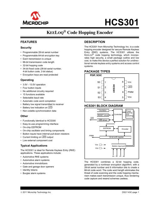
PACKAGE TYPES<br />
PDIP, SOIC<br />
<strong>HCS301</strong> BLOCK DIAGRAM<br />
LED<br />
PWM<br />
VSS<br />
VDD<br />
S0<br />
S1<br />
S2<br />
S3<br />
1<br />
2<br />
3<br />
4<br />
Oscillator<br />
RESET circuit<br />
LED driver<br />
EEPROM<br />
<strong>HCS301</strong><br />
Controller<br />
The <strong>HCS301</strong> combines a 32-bit hopping code,<br />
generated by a nonlinear encryption algorithm, with a<br />
28-bit serial number and 6 information bits to create a<br />
66-bit code word. The code word length eliminates the<br />
threat of code scanning and the code hopping mechanism<br />
makes each transmission unique, thus rendering<br />
code capture and resend schemes useless.<br />
8<br />
7<br />
6<br />
5<br />
32-bit shift register<br />
Button input port<br />
S3 S2 S1 S0<br />
<strong>Encoder</strong><br />
VDD<br />
LED<br />
PWM<br />
VSS<br />
Power<br />
latching<br />
and<br />
switching<br />
© 2011 <strong>Microchip</strong> Technology Inc. DS21143C-page 1
<strong>HCS301</strong><br />
The crypt key, serial number and configuration data are<br />
stored in an EEPROM array which is not accessible via<br />
any external connection. The EEPROM data is programmable<br />
but read-protected. The data can be verified<br />
only after an automatic erase and programming<br />
operation. This protects against attempts to gain<br />
access to keys or manipulate synchronization values.<br />
The <strong>HCS301</strong> provides an easy-to-use serial interface<br />
for programming the necessary keys, system parameters<br />
and configuration data.<br />
1.0 SYSTEM OVERVIEW<br />
Key Terms<br />
The following is a list of key terms used throughout this<br />
data sheet. For additional information on KEELOQ and<br />
<strong>Code</strong> <strong>Hopping</strong>, refer to Technical Brief 3 (TB003).<br />
• RKE - Remote Keyless Entry<br />
• Button Status - Indicates what button input(s)<br />
activated the transmission. Encompasses the 4<br />
button status bits S3, S2, S1 and S0 (Figure 4-2).<br />
• <strong>Code</strong> <strong>Hopping</strong> - A method by which a code,<br />
viewed externally to the system, appears to<br />
change unpredictably each time it is transmitted.<br />
• <strong>Code</strong> word - A block of data that is repeatedly<br />
transmitted upon button activation (Figure 4-1).<br />
• Transmission - A data stream consisting of<br />
repeating code words (Figure 9-2).<br />
• Crypt key - A unique and secret 64-bit number<br />
used to encrypt and decrypt data. In a symmetrical<br />
block cipher such as the KEELOQ algorithm,<br />
the encryption and decryption keys are equal and<br />
will therefore be referred to generally as the crypt<br />
key.<br />
• <strong>Encoder</strong> - A device that generates and encodes<br />
data.<br />
• Encryption Algorithm - A recipe whereby data is<br />
scrambled using a crypt key. The data can only be<br />
interpreted by the respective decryption algorithm<br />
using the same crypt key.<br />
• Decoder - A device that decodes data received<br />
from an encoder.<br />
• Decryption algorithm - A recipe whereby data<br />
scrambled by an encryption algorithm can be<br />
unscrambled using the same crypt key.<br />
• Learn – Learning involves the receiver calculating<br />
the transmitter’s appropriate crypt key, decrypting<br />
the received hopping code and storing the serial<br />
number, synchronization counter value and crypt<br />
key in EEPROM. The KEELOQ product family facilitates<br />
several learning strategies to be implemented<br />
on the decoder. The following are<br />
examples of what can be done.<br />
- Simple Learning<br />
The receiver uses a fixed crypt key, common<br />
to all components of all systems by the same<br />
manufacturer, to decrypt the received code<br />
word’s encrypted portion.<br />
- Normal Learning<br />
The receiver uses information transmitted<br />
during normal operation to derive the crypt<br />
key and decrypt the received code word’s<br />
encrypted portion.<br />
- Secure Learn<br />
The transmitter is activated through a special<br />
button combination to transmit a stored 60-bit<br />
seed value used to generate the transmitter’s<br />
crypt key. The receiver uses this seed value<br />
to derive the same crypt key and decrypt the<br />
received code word’s encrypted portion.<br />
• Manufacturer’s code – A unique and secret 64-<br />
bit number used to generate unique encoder crypt<br />
keys. Each encoder is programmed with a crypt<br />
key that is a function of the manufacturer’s code.<br />
Each decoder is programmed with the manufacturer<br />
code itself.<br />
The <strong>HCS301</strong> code hopping encoder is designed specifically<br />
for keyless entry systems; primarily vehicles and<br />
home garage door openers. The encoder portion of a<br />
keyless entry system is integrated into a transmitter,<br />
carried by the user and operated to gain access to a<br />
vehicle or restricted area. The <strong>HCS301</strong> is meant to be<br />
a cost-effective yet secure solution to such systems,<br />
requiring very few external components (Figure 2-1).<br />
Most low-end keyless entry transmitters are given a<br />
fixed identification code that is transmitted every time a<br />
button is pushed. The number of unique identification<br />
codes in a low-end system is usually a relatively small<br />
number. These shortcomings provide an opportunity<br />
for a sophisticated thief to create a device that ‘grabs’<br />
a transmission and retransmits it later, or a device that<br />
quickly ‘scans’ all possible identification codes until the<br />
correct one is found.<br />
The <strong>HCS301</strong>, on the other hand, employs the KEELOQ<br />
code hopping technology coupled with a transmission<br />
length of 66 bits to virtually eliminate the use of code<br />
‘grabbing’ or code ‘scanning’. The high security level of<br />
the <strong>HCS301</strong> is based on the patented KEELOQ technology.<br />
A block cipher based on a block length of 32 bits<br />
and a key length of 64 bits is used. The algorithm<br />
obscures the information in such a way that even if the<br />
transmission information (before coding) differs by only<br />
one bit from that of the previous transmission, the next<br />
DS21143C-page 2<br />
© 2011 <strong>Microchip</strong> Technology Inc.
<strong>HCS301</strong><br />
coded transmission will be completely different. Statistically,<br />
if only one bit in the 32-bit string of information<br />
changes, greater than 50 percent of the coded transmission<br />
bits will change.<br />
As indicated in the block diagram on page one, the<br />
<strong>HCS301</strong> has a small EEPROM array which must be<br />
loaded with several parameters before use; most often<br />
programmed by the manufacturer at the time of production.<br />
The most important of these are:<br />
• A 28-bit serial number, typically unique for every<br />
encoder<br />
• A crypt key<br />
• An initial 16-bit synchronization value<br />
• A 16-bit configuration value<br />
The crypt key generation typically inputs the transmitter<br />
serial number and 64-bit manufacturer’s code into the<br />
key generation algorithm (Figure 1-1). The manufacturer’s<br />
code is chosen by the system manufacturer and<br />
must be carefully controlled as it is a pivotal part of the<br />
overall system security.<br />
FIGURE 1-1:<br />
CREATION AND STORAGE OF CRYPT KEY DURING PRODUCTION<br />
Production<br />
Programmer<br />
Manufacturer’s<br />
<strong>Code</strong><br />
Transmitter<br />
Serial Number<br />
Key<br />
Generation<br />
Algorithm<br />
Crypt<br />
Key<br />
<strong>HCS301</strong><br />
EEPROM Array<br />
Serial Number<br />
Crypt Key<br />
Sync Counter<br />
.<br />
.<br />
.<br />
The 16-bit synchronization counter is the basis behind<br />
the transmitted code word changing for each transmission;<br />
it increments each time a button is pressed. Due<br />
to the code hopping algorithm’s complexity, each increment<br />
of the synchronization value results in greater<br />
than 50% of the bits changing in the transmitted code<br />
word.<br />
Figure 1-2 shows how the key values in EEPROM are<br />
used in the encoder. Once the encoder detects a button<br />
press, it reads the button inputs and updates the synchronization<br />
counter. The synchronization counter and<br />
crypt key are input to the encryption algorithm and the<br />
output is 32 bits of encrypted information. This data will<br />
change with every button press, its value appearing<br />
externally to ‘randomly hop around’, hence it is referred<br />
to as the hopping portion of the code word. The 32-bit<br />
hopping code is combined with the button information<br />
and serial number to form the code word transmitted to<br />
the receiver. The code word format is explained in<br />
greater detail in Section 4.0.<br />
A receiver may use any type of controller as a decoder,<br />
but it is typically a microcontroller with compatible firmware<br />
that allows the decoder to operate in conjunction<br />
with an <strong>HCS301</strong> based transmitter. Section 7.0<br />
provides detail on integrating the <strong>HCS301</strong> into a system.<br />
A transmitter must first be ‘learned’ by the receiver<br />
before its use is allowed in the system. Learning<br />
includes calculating the transmitter’s appropriate crypt<br />
key, decrypting the received hopping code and storing<br />
the serial number, synchronization counter value and<br />
crypt key in EEPROM.<br />
In normal operation, each received message of valid<br />
format is evaluated. The serial number is used to determine<br />
if it is from a learned transmitter. If from a learned<br />
transmitter, the message is decrypted and the synchronization<br />
counter is verified. Finally, the button status is<br />
checked to see what operation is requested. Figure 1-3<br />
shows the relationship between some of the values<br />
stored by the receiver and the values received from<br />
the transmitter.<br />
© 2011 <strong>Microchip</strong> Technology Inc. DS21143C-page 3
<strong>HCS301</strong><br />
FIGURE 1-2:<br />
BUILDING THE TRANSMITTED CODE WORD (ENCODER)<br />
EEPROM Array<br />
Crypt Key<br />
Sync Counter<br />
KEELOQ ®<br />
Encryption<br />
Algorithm<br />
Serial Number<br />
Button Press<br />
Information<br />
Serial Number<br />
32 Bits<br />
Encrypted Data<br />
Transmitted Information<br />
FIGURE 1-3:<br />
BASIC OPERATION OF RECEIVER (DECODER)<br />
1<br />
Received Information<br />
EEPROM Array<br />
Button Press<br />
Information<br />
Serial Number<br />
32 Bits of<br />
Encrypted Data<br />
Manufacturer <strong>Code</strong><br />
2<br />
Check for<br />
Match<br />
Serial Number<br />
Sync Counter<br />
Crypt Key<br />
3<br />
KEELOQ ®<br />
Decryption<br />
Algorithm<br />
Perform Function<br />
5<br />
Indicated by<br />
button press<br />
Decrypted<br />
Synchronization<br />
Counter<br />
4<br />
Check for<br />
Match<br />
NOTE: Circled numbers indicate the order of execution.<br />
DS21143C-page 4<br />
© 2011 <strong>Microchip</strong> Technology Inc.
<strong>HCS301</strong><br />
2.0 DEVICE OPERATION<br />
TABLE 2-1:<br />
PIN DESCRIPTIONS<br />
As shown in the typical application circuits (Figure 2-1),<br />
the <strong>HCS301</strong> is a simple device to use. It requires only<br />
the addition of buttons and RF circuitry for use as the<br />
transmitter in your security application. A description of<br />
each pin is given in Table 2-1.<br />
Note:<br />
FIGURE 2-1:<br />
When VDD > 9.0V and driving low capacitive<br />
loads, a resistor with a minimum value<br />
of 50Ω should be used in line with VDD.<br />
This prevents clamping of PWM at 9.0V in<br />
the event of PWM overshoot.<br />
B0<br />
B1<br />
+12V<br />
(2)<br />
R<br />
TYPICAL CIRCUITS<br />
S0<br />
S1<br />
S2<br />
S3<br />
2 button remote control<br />
B4 B3 B2 B1 B0<br />
S0<br />
S1<br />
S2<br />
S3<br />
5 button remote control (1)<br />
VDD<br />
LED<br />
PWM<br />
VSS<br />
VDD<br />
LED<br />
PWM<br />
VSS<br />
+12V<br />
(2)<br />
R<br />
Tx out<br />
Tx out<br />
Note 1: Up to 15 functions can be implemented by pressing<br />
more than one button simultaneously or by using a<br />
suitable diode array.<br />
Name<br />
Pin<br />
Number<br />
Description<br />
S0 1 Switch input 0<br />
S1 2 Switch input 1<br />
S2 3 Switch input 2 / Clock pin when in<br />
Programming mode<br />
S3 4 Switch input 3<br />
VSS 5 Ground reference<br />
PWM 6 Pulse Width Modulation (PWM)<br />
output pin / Data pin for<br />
Programming mode<br />
LED 7 Cathode connection for LED<br />
VDD 8 Positive supply voltage<br />
The <strong>HCS301</strong> will wake-up upon detecting a button<br />
press and delay approximately 10 ms for button<br />
debounce (Figure 2-2). The synchronization counter,<br />
discrimination value and button information will be<br />
encrypted to form the hopping code. The hopping code<br />
portion will change every transmission, even if the<br />
same button is pushed again. A code word that has<br />
been transmitted will not repeat for more than 64K<br />
transmissions. This provides more than 18 years of use<br />
before a code is repeated; based on 10 operations per<br />
day. Overflow information sent from the encoder can be<br />
used to extend the number of unique transmissions to<br />
more than 192K.<br />
If in the transmit process it is detected that a new button(s)<br />
has been pressed, a RESET will immediately<br />
occur and the current code word will not be completed.<br />
Please note that buttons removed will not have any<br />
effect on the code word unless no buttons remain<br />
pressed; in which case the code word will be completed<br />
and the power-down will occur.<br />
2: Resistor R is recommended for current limiting.<br />
© 2011 <strong>Microchip</strong> Technology Inc. DS21143C-page 5
<strong>HCS301</strong><br />
FIGURE 2-2: ENCODER OPERATION 3.0 EEPROM MEMORY<br />
ORGANIZATION<br />
Power-Up<br />
(A button has been pressed)<br />
RESET and Debounce Delay<br />
(10 ms)<br />
Sample Inputs<br />
The <strong>HCS301</strong> contains 192 bits (12 x 16-bit words) of<br />
EEPROM memory (Table 3-1). This EEPROM array is<br />
used to store the encryption key information,<br />
synchronization value, etc. Further descriptions of the<br />
memory array is given in the following sections.<br />
Yes<br />
Update Sync Info<br />
Encrypt With<br />
Crypt Key<br />
Load Transmit Register<br />
Transmit<br />
Buttons<br />
Added<br />
?<br />
No<br />
All<br />
Buttons<br />
Released<br />
?<br />
Yes<br />
Complete <strong>Code</strong><br />
Word Transmission<br />
Stop<br />
No<br />
TABLE 3-1:<br />
EEPROM MEMORY MAP<br />
WORD<br />
ADDRESS<br />
MNEMONIC DESCRIPTION<br />
0 KEY_0 64-bit encryption key<br />
(word 0) LSb’s<br />
1 KEY_1 64-bit encryption key<br />
(word 1)<br />
2 KEY_2 64-bit encryption key<br />
(word 2)<br />
3 KEY_3 64-bit encryption key<br />
(word 3) MSb’s<br />
4 SYNC 16-bit synchronization<br />
value<br />
5 RESERVED Set to 0000H<br />
6 SER_0 Device Serial Number<br />
(word 0) LSb’s<br />
7 SER_1(Note) Device Serial Number<br />
(word 1) MSb’s<br />
8 SEED_0 Seed Value (word 0)<br />
9 SEED_1 Seed Value (word 1)<br />
10 RESERVED Set to 0000H<br />
11 CONFIG Config Word<br />
Note:<br />
The MSB of the serial number contains a bit<br />
used to select the Auto-shutoff timer.<br />
3.1 KEY_0 - KEY_3 (64-Bit Crypt Key)<br />
The 64-bit crypt key is used to create the encrypted<br />
message transmitted to the receiver. This key is calculated<br />
and programmed during production using a key<br />
generation algorithm. The key generation algorithm<br />
may be different from the KEELOQ algorithm. Inputs to<br />
the key generation algorithm are typically the transmitter’s<br />
serial number and the 64-bit manufacturer’s code.<br />
While the key generation algorithm supplied from<br />
<strong>Microchip</strong> is the typical method used, a user may elect<br />
to create their own method of key generation. This may<br />
be done providing that the decoder is programmed with<br />
the same means of creating the key for<br />
decryption purposes.<br />
DS21143C-page 6<br />
© 2011 <strong>Microchip</strong> Technology Inc.
<strong>HCS301</strong><br />
3.2 SYNC (Synchronization Counter)<br />
This is the 16-bit synchronization value that is used to<br />
create the hopping code for transmission. This value<br />
will increment after every transmission.<br />
3.3 Reserved<br />
Must be initialized to 0000H.<br />
3.4 SER_0, SER_1<br />
(<strong>Encoder</strong> Serial Number)<br />
SER_0 and SER_1 are the lower and upper words of<br />
the device serial number, respectively. Although there<br />
are 32 bits allocated for the serial number, only the<br />
lower order 28 bits are transmitted. The serial number<br />
is meant to be unique for every transmitter.<br />
3.4.1 AUTO-SHUTOFF TIMER ENABLE<br />
The Most Significant bit of the serial number (Bit 31) is<br />
used to turn the Auto-shutoff timer on or off. This timer<br />
prevents the transmitter from draining the battery<br />
should a button get stuck in the on position for a long<br />
period of time. The time period is approximately<br />
25 seconds, after which the device will go to the Timeout<br />
mode. When in the Time-out mode, the device will<br />
stop transmitting, although since some circuits within<br />
the device are still active, the current draw within the<br />
Shutoff mode will be higher than Standby mode. If the<br />
Most Significant bit in the serial number is a one, then<br />
the Auto-shutoff timer is enabled, and a zero in the<br />
Most Significant bit will disable the timer. The length of<br />
the timer is not selectable.<br />
3.5 SEED_0, SEED_1 (Seed Word)<br />
The 2-word (32-bit) seed code will be transmitted when<br />
all three buttons are pressed at the same time (see<br />
Figure 4-2). This allows the system designer to implement<br />
the secure learn feature or use this fixed code<br />
word as part of a different key generation/tracking process.<br />
3.6 CONFIG (Configuration Word)<br />
The Configuration Word is a 16-bit word stored in<br />
EEPROM array that is used by the device to store<br />
information used during the encryption process, as well<br />
as the status of option configurations. The following<br />
sections further explain these bits.<br />
TABLE 3-2:<br />
CONFIGURATION WORD<br />
Bit Number<br />
Bit Description<br />
0 Discrimination Bit 0<br />
1 Discrimination Bit 1<br />
2 Discrimination Bit 2<br />
3 Discrimination Bit 3<br />
4 Discrimination Bit 4<br />
5 Discrimination Bit 5<br />
6 Discrimination Bit 6<br />
7 Discrimination Bit 7<br />
8 Discrimination Bit 8<br />
9 Discrimination Bit 9<br />
10 Overflow Bit 0 (OVR0)<br />
11 Overflow Bit 1 (OVR1)<br />
12 Low Voltage Trip Point Select<br />
(VLOW SEL)<br />
13 Baud rate Select Bit 0 (BSL0)<br />
14 Baud rate Select Bit 1 (BSL1)<br />
15 Reserved, set to 0<br />
3.6.1 DISCRIMINATION VALUE<br />
(DISC0 TO DISC9)<br />
The discrimination value aids the post-decryption<br />
check on the decoder end. It may be any value, but in<br />
a typical system it will be programmed as the 10 Least<br />
Significant bits of the serial number. Values other than<br />
this must be separately stored by the receiver when a<br />
transmitter is learned. The discrimination bits are part<br />
of the information that form the encrypted portion of the<br />
transmission (Figure 4-2). After the receiver has<br />
decrypted a transmission, the discrimination bits are<br />
checked against the receiver’s stored value to verify<br />
that the decryption process was valid. If the discrimination<br />
value was programmed as the 10 LSb’s of the<br />
serial number then it may merely be compared to the<br />
respective bits of the received serial number; saving<br />
EEPROM space.<br />
3.6.2 OVERFLOW BITS<br />
(OVR0, OVR1)<br />
The overflow bits are used to extend the number of<br />
possible synchronization values. The synchronization<br />
counter is 16 bits in length, yielding 65,536 values<br />
before the cycle repeats. Under typical use of<br />
10 operations a day, this will provide nearly 18 years of<br />
use before a repeated value will be used. Should the<br />
system designer conclude that is not adequate, then<br />
the overflow bits can be utilized to extend the number<br />
© 2011 <strong>Microchip</strong> Technology Inc. DS21143C-page 7
<strong>HCS301</strong><br />
of unique values. This can be done by programming<br />
OVR0 and OVR1 to 1s at the time of production. The<br />
encoder will automatically clear OVR0 the first time that<br />
the synchronization value wraps from 0xFFFF to<br />
0x0000 and clear OVR1 the second time the counter<br />
wraps. Once cleared, OVR0 and OVR1 cannot be set<br />
again, thereby creating a permanent record of the<br />
counter overflow. This prevents fast cycling of 64K<br />
counter. If the decoder system is programmed to track<br />
the overflow bits, then the effective number of unique<br />
synchronization values can be extended to 196,608.<br />
3.6.4 LOW VOLTAGE TRIP POINT<br />
SELECT<br />
The low voltage trip point select bit is used to tell the<br />
<strong>HCS301</strong> what VDD level is being used. This information<br />
will be used by the device to determine when to send the<br />
voltage low signal to the receiver. When this bit is set to<br />
a one, the VDD level is assumed to be operating from a<br />
9V or 12V VDD level. If the bit is set low, then the VDD level<br />
is assumed to be 6.0 volts. Refer to Figure 3-1 for voltage<br />
trip point.<br />
3.6.3 BAUD RATE SELECT BITS<br />
(BSL0, BSL1)<br />
BSL0 and BSL1 select the speed of transmission and<br />
the code word blanking. Table 3-3 shows how the bits<br />
are used to select the different baud rates and<br />
Section 5.7 provides detailed explanation in code word<br />
blanking.<br />
TABLE 3-3:<br />
BSL1<br />
BSL0<br />
BAUD RATE SELECT<br />
Basic Pulse<br />
Element<br />
<strong>Code</strong> Words<br />
Transmitted<br />
0 0 400 μs All<br />
0 1 200 μs 1 out of 2<br />
1 0 100 μs 1 out of 2<br />
1 1 100 μs 1 out of 4<br />
FIGURE 3-1:<br />
Volts (V)<br />
5.5<br />
5.0<br />
4.5<br />
4.0<br />
3.5<br />
3.0<br />
2.5<br />
9.0<br />
8.5<br />
8.0<br />
7.5<br />
7.0<br />
VOLTAGE TRIP POINTS<br />
BY CHARACTERIZATION<br />
VLOW sel = 0<br />
VLOW sel = 1<br />
VLOW<br />
Max<br />
Min<br />
Max<br />
Min<br />
-40 -20 0 20 40 60 80 100<br />
Temp (C)<br />
DS21143C-page 8<br />
© 2011 <strong>Microchip</strong> Technology Inc.
<strong>HCS301</strong><br />
4.0 TRANSMITTED WORD<br />
4.1 <strong>Code</strong> Word Format<br />
The <strong>HCS301</strong> code word is made up of several parts<br />
(Figure 4-1). Each code word contains a 50% duty<br />
cycle preamble, a header, 32 bits of encrypted data and<br />
34 bits of fixed data followed by a guard period before<br />
another code word can begin. Refer to Table 9-4 for<br />
code word timing.<br />
4.2 <strong>Code</strong> Word Organization<br />
The <strong>HCS301</strong> transmits a 66-bit code word when a<br />
button is pressed. The 66-bit word is constructed from<br />
a Fixed <strong>Code</strong> portion and an Encrypted <strong>Code</strong> portion<br />
(Figure 4-2).<br />
The 32 bits of Encrypted Data are generated from 4<br />
button bits, 12 discrimination bits and the 16-bit sync<br />
value. The encrypted portion alone provides up to four<br />
billion changing code combinations.<br />
The 34 bits of Fixed <strong>Code</strong> Data are made up of 2 status<br />
bits, 4 button bits and the 28-bit serial number. The<br />
fixed and encrypted sections combined increase the<br />
number of code combinations to 7.38 x 10 19 .<br />
FIGURE 4-1:<br />
CODE WORD FORMAT<br />
TE<br />
TE<br />
TE<br />
LOGIC ‘0’<br />
LOGIC ‘1’<br />
Bit<br />
Period<br />
50% Duty Cycle<br />
Encrypted Portion Fixed Portion of Guard<br />
Preamble Header of Transmission Transmission Time<br />
TP TH THOP TFIX TG<br />
FIGURE 4-2:<br />
CODE WORD ORGANIZATION<br />
34 bits of Fixed Portion 32 bits of Encrypted Portion<br />
MSb<br />
Repeat<br />
(1 bit)<br />
VLOW<br />
(1 bit)<br />
Button<br />
Status<br />
S2 S1 S0 S3<br />
Serial Number<br />
(28 bits)<br />
Button<br />
Status<br />
S2 S1 S0 S3<br />
OVR<br />
(2 bits)<br />
DISC<br />
(10 bits)<br />
Sync Counter<br />
(16 bits)<br />
66 Data bits<br />
Transmitted<br />
LSb first.<br />
LSb<br />
MSb<br />
Repeat<br />
(1 bit)<br />
VLOW<br />
(1 bit)<br />
Button<br />
Status<br />
1 1 1 1<br />
Serial Number<br />
(28 bits)<br />
SEED<br />
(32 bits)<br />
Note: SEED replaces Encrypted Portion when all button inputs are activated at the same time.<br />
LSb<br />
© 2011 <strong>Microchip</strong> Technology Inc. DS21143C-page 9
<strong>HCS301</strong><br />
4.3 Synchronous Transmission Mode<br />
Synchronous Transmission mode can be used to clock<br />
the code word out using an external clock.<br />
To enter Synchronous Transmission mode, the Programming<br />
mode start-up sequence must be executed<br />
as shown in Figure 4-3. If either S1 or S0 is set on the<br />
falling edge of S2 (or S3), the device enters Synchronous<br />
Transmission mode. In this mode, it functions as<br />
a normal transmitter, with the exception that the timing<br />
of the PWM data string is controlled externally and 16<br />
extra bits are transmitted at the end with the code word.<br />
The button code will be the S0, S1 value at the falling<br />
edge of S2 or S3. The timing of the PWM data string is<br />
controlled by supplying a clock on S2 or S3 and should<br />
not exceed 20 kHz. The code word is the same as in<br />
PWM mode with 16 reserved bits at the end of the<br />
word. The reserved bits can be ignored. When in Synchronous<br />
Transmission mode S2 or S3 should not be<br />
toggled until all internal processing has been completed<br />
as shown in Figure 4-4.<br />
FIGURE 4-3:<br />
SYNCHRONOUS TRANSMISSION MODE<br />
TPS TPH1 TPH2 t = 50ms Preamble Header Data<br />
PWM<br />
S2<br />
S[1:0]<br />
“01,10,11”<br />
FIGURE 4-4:<br />
CODE WORD ORGANIZATION (SYNCHRONOUS TRANSMISSION MODE)<br />
Fixed Portion<br />
Encrypted Portion<br />
MSb<br />
Reserved<br />
(16 bits)<br />
Padding<br />
(2 bits)<br />
Button<br />
Status<br />
S2 S1 S0 S3<br />
Serial Number<br />
(28 bits)<br />
Button<br />
Status<br />
S2 S1 S0 S3<br />
DISC+ OVR<br />
(12 bits)<br />
82 Data bits<br />
Transmitted<br />
LSb first.<br />
Sync Counter<br />
(16 bits)<br />
LSb<br />
DS21143C-page 10<br />
© 2011 <strong>Microchip</strong> Technology Inc.
<strong>HCS301</strong><br />
5.0 SPECIAL FEATURES<br />
5.1 <strong>Code</strong> Word Completion<br />
The code word completion feature ensures that entire<br />
code words are transmitted, even if the button is<br />
released before the code word is complete. If the button<br />
is held down beyond the time for one code word,<br />
multiple code words will result. If another button is activated<br />
during a transmission, the active transmission<br />
will be aborted and a new transmission will begin using<br />
the new button information.<br />
5.2 LED Output Operation<br />
During normal transmission the LED output is LOW. If<br />
the supply voltage drops below the low voltage trip<br />
point, the LED output will be toggled at approximately<br />
5Hz during the transmission (Section 3.6.4).<br />
5.3 RPT: Repeat Indicator<br />
This bit will be low for the first transmitted word. If a<br />
button is held down for more than one transmitted code<br />
word, this bit will be set to indicate a repeated code<br />
word and remain set until the button is released.<br />
5.6 Seed Transmission<br />
In order to increase the level of security in a system, it<br />
is possible for the receiver to implement what is known<br />
as a secure learn function. This can be done by utilizing<br />
the seed value stored in EEPROM, transmitted only<br />
when all three button inputs are pressed at the same<br />
time (Table 5-1). Instead of the normal key generation<br />
inputs being used to create the crypt key, this seed<br />
value is used.<br />
TABLE 5-1:<br />
PIN ACTIVATION TABLE<br />
Function S3 S2 S1 S0<br />
Standby 0 0 0 0 0<br />
1 0 0 0 1<br />
<strong>Hopping</strong> <strong>Code</strong><br />
2 0 0 1 0<br />
- - - - -<br />
13 1 1 0 1<br />
14 1 1 1 0<br />
Seed <strong>Code</strong> 15 1 1 1 1<br />
5.4 VLOW: Voltage LOW Indicator<br />
The VLOW signal is transmitted so the receiver can give<br />
an indication to the user that the transmitter battery is<br />
low. The VLOW bit is included in every transmission<br />
(Figure 4-2 and Figure 9-5) and will be transmitted as a<br />
zero if the operating voltage is above the low voltage<br />
trip point. Refer to Figure 4-2. The trip point is selectable<br />
based on the battery voltage being used. See Section<br />
3.6.3 for a description of how the low voltage trip<br />
point is configured.<br />
5.5 Auto-shutoff<br />
The Auto-shutoff function automatically stops the<br />
device from transmitting if a button inadvertently gets<br />
pressed for a long period of time. This will prevent the<br />
device from draining the battery if a button gets<br />
pressed while the transmitter is in a pocket or purse.<br />
This function can be enabled or disabled and is<br />
selected by setting or clearing the Auto-shutoff bit (see<br />
Section 3.4.1). Setting this bit high will enable the function<br />
(turn Auto-shutoff function on) and setting the bit<br />
low will disable the function. Time-out period is approximately<br />
25 seconds.<br />
© 2011 <strong>Microchip</strong> Technology Inc. DS21143C-page 11
<strong>HCS301</strong><br />
5.7 Blank Alternate <strong>Code</strong> Word<br />
Federal Communications Commission (FCC) part 15<br />
rules specify the limits on worst case average fundamental<br />
power and harmonics that can be transmitted in<br />
a 100 ms window. For FCC approval purposes, it may<br />
therefore be advantageous to minimize the transmission<br />
duty cycle. This can be achieved by minimizing the<br />
duty cycle of the individual bits as well as by blanking<br />
out consecutive code words. Blank Alternate <strong>Code</strong><br />
Word (BACW) may be used to reduce the average<br />
power of a transmission by transmitting only every second<br />
code word (Figure 5-1). This is a selectable feature<br />
that is determined in conjunction with the baud rate<br />
selection bit BSL0.<br />
Enabling the BACW option may likewise allow the user<br />
to transmit a higher amplitude transmission as the time<br />
averaged power is reduced. BACW effectively halves<br />
the RF on time for a given transmission so the RF output<br />
power could theoretically be doubled while maintaining<br />
the same time averaged output power.<br />
FIGURE 5-1:<br />
BLANK ALTERNATE CODE WORD (BACW)<br />
Amplitude<br />
BACW Disabled<br />
(All words transmitted)<br />
A<br />
<strong>Code</strong> Word<br />
<strong>Code</strong> Word <strong>Code</strong> Word <strong>Code</strong> Word<br />
BACW Enabled<br />
(1 out of 2 transmitted)<br />
2A<br />
BACW Enabled<br />
(1 out of 4 transmitted)<br />
4A<br />
Time<br />
DS21143C-page 12<br />
© 2011 <strong>Microchip</strong> Technology Inc.
<strong>HCS301</strong><br />
6.0 PROGRAMMING THE <strong>HCS301</strong><br />
When using the <strong>HCS301</strong> in a system, the user will have<br />
to program some parameters into the device including<br />
the serial number and the secret key before it can be<br />
used. The programming cycle allows the user to input<br />
all 192 bits in a serial data stream, which are then<br />
stored internally in EEPROM. Programming will be<br />
initiated by forcing the PWM line high, after the S2 (or<br />
S3) line has been held high for the appropriate length<br />
of time line (Table 6-1 and Figure 6-1). After the Program<br />
mode is entered, a delay must be provided to the<br />
device for the automatic bulk write cycle to complete.<br />
This will set all locations in the EEPROM to zeros. The<br />
device can then be programmed by clocking in 16 bits<br />
at a time, using S2 (or S3) as the clock line and PWM<br />
as the data in line. After each 16-bit word is loaded, a<br />
programming delay is required for the internal program<br />
cycle to complete. This delay can take up to TWC. At the<br />
end of the programming cycle, the device can be verified<br />
(Figure 6-2) by reading back the EEPROM. Reading<br />
is done by clocking the S2 (or S3) line and reading<br />
the data bits on PWM. For security reasons, it is not<br />
possible to execute a verify function without first programming<br />
the EEPROM. A Verify operation can only<br />
be done once, immediately following the Program<br />
cycle.<br />
Note:<br />
To ensure that the device does not accidentally<br />
enter Programming mode, PWM<br />
should never be pulled high by the circuit<br />
connected to it. Special care should be<br />
taken when driving PNP RF transistors.<br />
FIGURE 6-1: PROGRAMMING WAVEFORMS<br />
Enter Program<br />
Mode TPBW<br />
TCLKH<br />
TDS<br />
TWC<br />
S2 (S3)<br />
(Clock)<br />
PWM<br />
(Data)<br />
TPS<br />
TPH1<br />
TCLKL TDH<br />
Bit 0 Bit 1 Bit 2 Bit 3 Bit 14 Bit 15 Bit 16 Bit 17<br />
TPH2<br />
Data for Word 0 (KEY_0) Data for Word 1<br />
Repeat for each word (12 times)<br />
Note 1: Unused button inputs to be held to ground during the entire programming sequence.<br />
2: The VDD pin must be taken to ground after a Program/Verify cycle.<br />
FIGURE 6-2:<br />
VERIFY WAVEFORMS<br />
End of Programming Cycle<br />
Beginning of Verify Cycle<br />
Data from Word 0<br />
PWM<br />
(Data)<br />
Bit190 Bit191<br />
TWC<br />
Bit 0<br />
Bit 1 Bit 2 Bit 3 Bit 14 Bit 15 Bit 16 Bit 17 Bit190 Bit191<br />
TDV<br />
S2 (S3)<br />
(Clock)<br />
Note: If a Verify operation is to be done, then it must immediately follow the Program cycle.<br />
© 2011 <strong>Microchip</strong> Technology Inc. DS21143C-page 13
<strong>HCS301</strong><br />
TABLE 6-1:<br />
PROGRAMMING/VERIFY TIMING REQUIREMENTS<br />
VDD = 5.0V ± 10%, 25 °C ± 5 °C<br />
Parameter Symbol Min. Max. Units<br />
Program mode setup time TPS 3.5 4.5 ms<br />
Hold time 1 TPH1 3.5 — ms<br />
Hold time 2 TPH2 50 — μs<br />
Bulk Write time TPBW 4.0 — ms<br />
Program delay time TPROG 4.0 — ms<br />
Program cycle time TWC 50 — ms<br />
Clock low time TCLKL 50 — μs<br />
Clock high time TCLKH 50 — μs<br />
Data setup time TDS 0 — μs (1)<br />
Data hold time TDH 30 — μs (1)<br />
Data out valid time TDV — 30 μs (1)<br />
Note 1: Typical values - not tested in production.<br />
DS21143C-page 14<br />
© 2011 <strong>Microchip</strong> Technology Inc.
<strong>HCS301</strong><br />
7.0 INTEGRATING THE <strong>HCS301</strong><br />
INTO A SYSTEM<br />
Use of the <strong>HCS301</strong> in a system requires a compatible<br />
decoder. This decoder is typically a microcontroller with<br />
compatible firmware. <strong>Microchip</strong> will provide (via a<br />
license agreement) firmware routines that accept<br />
transmissions from the <strong>HCS301</strong> and decrypt the<br />
hopping code portion of the data stream. These<br />
routines provide system designers the means to<br />
develop their own decoding system.<br />
7.1 Learning a Transmitter to a<br />
Receiver<br />
A transmitter must first be 'learned' by a decoder before<br />
its use is allowed in the system. Several learning strategies<br />
are possible, Figure 7-1 details a typical learn<br />
sequence. Core to each, the decoder must minimally<br />
store each learned transmitter's serial number and current<br />
synchronization counter value in EEPROM. Additionally,<br />
the decoder typically stores each transmitter's<br />
unique crypt key. The maximum number of learned<br />
transmitters will therefore be relative to the available<br />
EEPROM.<br />
A transmitter's serial number is transmitted in the clear<br />
but the synchronization counter only exists in the code<br />
word's encrypted portion. The decoder obtains the<br />
counter value by decrypting using the same key used<br />
to encrypt the information. The KEELOQ algorithm is a<br />
symmetrical block cipher so the encryption and decryption<br />
keys are identical and referred to generally as the<br />
crypt key. The encoder receives its crypt key during<br />
manufacturing. The decoder is programmed with the<br />
ability to generate a crypt key as well as all but one<br />
required input to the key generation routine; typically<br />
the transmitter's serial number.<br />
Figure 7-1 summarizes a typical learn sequence. The<br />
decoder receives and authenticates a first transmission;<br />
first button press. Authentication involves generating<br />
the appropriate crypt key, decrypting, validating<br />
the correct key usage via the discrimination bits and<br />
buffering the counter value. A second transmission is<br />
received and authenticated. A final check verifies the<br />
counter values were sequential; consecutive button<br />
presses. If the learn sequence is successfully complete,<br />
the decoder stores the learned transmitter's<br />
serial number, current synchronization counter value<br />
and appropriate crypt key. From now on the crypt key<br />
will be retrieved from EEPROM during normal operation<br />
instead of recalculating it for each transmission<br />
received.<br />
Certain learning strategies have been patented and<br />
care must be taken not to infringe.<br />
FIGURE 7-1:<br />
Enter Learn<br />
Mode<br />
Wait for Reception<br />
of a Valid <strong>Code</strong><br />
Generate Key<br />
from Serial Number<br />
Use Generated Key<br />
to Decrypt<br />
Compare Discrimination<br />
Value with Fixed Value<br />
Equal<br />
?<br />
Yes<br />
Wait for Reception<br />
of Second Valid <strong>Code</strong><br />
Use Generated Key<br />
to Decrypt<br />
Compare Discrimination<br />
Value with Fixed Value<br />
Equal<br />
?<br />
Counters<br />
Sequential<br />
?<br />
Yes<br />
Learn successful Store:<br />
Serial number<br />
Encryption key<br />
Synchronization counter<br />
Exit<br />
Yes<br />
TYPICAL LEARN<br />
SEQUENCE<br />
No<br />
No<br />
No<br />
Learn<br />
Unsuccessful<br />
© 2011 <strong>Microchip</strong> Technology Inc. DS21143C-page 15
<strong>HCS301</strong><br />
7.2 Decoder Operation<br />
Figure 7-2 summarizes normal decoder operation. The<br />
decoder waits until a transmission is received. The<br />
received serial number is compared to the EEPROM<br />
table of learned transmitters to first determine if this<br />
transmitter's use is allowed in the system. If from a<br />
learned transmitter, the transmission is decrypted<br />
using the stored crypt key and authenticated via the<br />
discrimination bits for appropriate crypt key usage. If<br />
the decryption was valid the synchronization value is<br />
evaluated.<br />
FIGURE 7-2:<br />
No<br />
Transmission<br />
Received<br />
?<br />
Does<br />
No Serial Number<br />
Match<br />
?<br />
Yes<br />
Decrypt Transmission<br />
No<br />
No<br />
No<br />
Start<br />
Is<br />
Decryption<br />
Valid<br />
?<br />
Is<br />
Counter<br />
Within 16<br />
?<br />
Is<br />
Counter<br />
Within 32K<br />
?<br />
Yes<br />
Save Counter<br />
in Temp Location<br />
TYPICAL DECODER<br />
OPERATION<br />
Yes<br />
Yes<br />
No<br />
Yes<br />
Execute<br />
Command<br />
and<br />
Update<br />
Counter<br />
7.3 Synchronization with Decoder<br />
(Evaluating the Counter)<br />
The KEELOQ technology patent scope includes a<br />
sophisticated synchronization technique that does not<br />
require the calculation and storage of future codes. The<br />
technique securely blocks invalid transmissions while<br />
providing transparent resynchronization to transmitters<br />
inadvertently activated away from the receiver.<br />
Figure 7-3 shows a 3-partition, rotating synchronization<br />
window. The size of each window is optional but the<br />
technique is fundamental. Each time a transmission is<br />
authenticated, the intended function is executed and<br />
the transmission's synchronization counter value is<br />
stored in EEPROM. From the currently stored counter<br />
value there is an initial "Single Operation" forward window<br />
of 16 codes. If the difference between a received<br />
synchronization counter and the last stored counter is<br />
within 16, the intended function will be executed on the<br />
single button press and the new synchronization counter<br />
will be stored. Storing the new synchronization<br />
counter value effectively rotates the entire synchronization<br />
window.<br />
A "Double Operation" (resynchronization) window further<br />
exists from the Single Operation window up to 32K<br />
codes forward of the currently stored counter value. It<br />
is referred to as "Double Operation" because a transmission<br />
with synchronization counter value in this window<br />
will require an additional, sequential counter<br />
transmission prior to executing the intended function.<br />
Upon receiving the sequential transmission the<br />
decoder executes the intended function and stores the<br />
synchronization counter value. This resynchronization<br />
occurs transparently to the user as it is human nature<br />
to press the button a second time if the first was unsuccessful.<br />
The third window is a "Blocked Window" ranging from<br />
the double operation window to the currently stored<br />
synchronization counter value. Any transmission with<br />
synchronization counter value within this window will<br />
be ignored. This window excludes previously used,<br />
perhaps code-grabbed transmissions from accessing<br />
the system.<br />
Note:<br />
The synchronization method described in<br />
this section is only a typical implementation<br />
and because it is usually implemented in<br />
firmware, it can be altered to fit the needs<br />
of a particular system.<br />
DS21143C-page 16<br />
© 2011 <strong>Microchip</strong> Technology Inc.
<strong>HCS301</strong><br />
FIGURE 7-3:<br />
SYNCHRONIZATION WINDOW<br />
Entire Window<br />
rotates to eliminate<br />
use of previously<br />
used codes<br />
Blocked<br />
Window<br />
(32K <strong>Code</strong>s)<br />
Double Operation<br />
(resynchronization)<br />
Window<br />
(32K <strong>Code</strong>s)<br />
Stored<br />
Synchronization<br />
Counter Value<br />
Single Operation<br />
Window<br />
(16 <strong>Code</strong>s)<br />
© 2011 <strong>Microchip</strong> Technology Inc. DS21143C-page 17
<strong>HCS301</strong><br />
8.0 DEVELOPMENT SUPPORT<br />
The PIC ® microcontrollers and dsPIC ® digital signal<br />
controllers are supported with a full range of software<br />
and hardware development tools:<br />
• Integrated Development Environment<br />
- MPLAB ® IDE Software<br />
• Compilers/Assemblers/Linkers<br />
- MPLAB C Compiler for Various Device<br />
Families<br />
- HI-TECH C for Various Device Families<br />
- MPASM TM Assembler<br />
- MPLINK TM Object Linker/<br />
MPLIB TM Object Librarian<br />
- MPLAB Assembler/Linker/Librarian for<br />
Various Device Families<br />
• Simulators<br />
- MPLAB SIM Software Simulator<br />
• Emulators<br />
- MPLAB REAL ICE In-Circuit Emulator<br />
• In-Circuit Debuggers<br />
- MPLAB ICD 3<br />
- PICkit 3 Debug Express<br />
• Device Programmers<br />
- PICkit 2 Programmer<br />
- MPLAB PM3 Device Programmer<br />
• Low-Cost Demonstration/Development Boards,<br />
Evaluation Kits, and Starter Kits<br />
8.1 MPLAB Integrated Development<br />
Environment Software<br />
The MPLAB IDE software brings an ease of software<br />
development previously unseen in the 8/16/32-bit<br />
microcontroller market. The MPLAB IDE is a Windows ®<br />
operating system-based application that contains:<br />
• A single graphical interface to all debugging tools<br />
- Simulator<br />
- Programmer (sold separately)<br />
- In-Circuit Emulator (sold separately)<br />
- In-Circuit Debugger (sold separately)<br />
• A full-featured editor with color-coded context<br />
• A multiple project manager<br />
• Customizable data windows with direct edit of<br />
contents<br />
• High-level source code debugging<br />
• Mouse over variable inspection<br />
• Drag and drop variables from source to watch<br />
windows<br />
• Extensive on-line help<br />
• Integration of select third party tools, such as<br />
IAR C Compilers<br />
The MPLAB IDE allows you to:<br />
• Edit your source files (either C or assembly)<br />
• One-touch compile or assemble, and download to<br />
emulator and simulator tools (automatically<br />
updates all project information)<br />
• Debug using:<br />
- Source files (C or assembly)<br />
- Mixed C and assembly<br />
- Machine code<br />
MPLAB IDE supports multiple debugging tools in a<br />
single development paradigm, from the cost-effective<br />
simulators, through low-cost in-circuit debuggers, to<br />
full-featured emulators. This eliminates the learning<br />
curve when upgrading to tools with increased flexibility<br />
and power.<br />
DS21143C-page 18<br />
© 2011 <strong>Microchip</strong> Technology Inc.
<strong>HCS301</strong><br />
8.2 MPLAB C Compilers for Various<br />
Device Families<br />
The MPLAB C Compiler code development systems<br />
are complete ANSI C compilers for <strong>Microchip</strong>’s PIC18,<br />
PIC24 and PIC32 families of microcontrollers and the<br />
dsPIC30 and dsPIC33 families of digital signal controllers.<br />
These compilers provide powerful integration<br />
capabilities, superior code optimization and ease of<br />
use.<br />
For easy source level debugging, the compilers provide<br />
symbol information that is optimized to the MPLAB IDE<br />
debugger.<br />
8.3 HI-TECH C for Various Device<br />
Families<br />
The HI-TECH C Compiler code development systems<br />
are complete ANSI C compilers for <strong>Microchip</strong>’s PIC<br />
family of microcontrollers and the dsPIC family of digital<br />
signal controllers. These compilers provide powerful<br />
integration capabilities, omniscient code generation<br />
and ease of use.<br />
For easy source level debugging, the compilers provide<br />
symbol information that is optimized to the MPLAB IDE<br />
debugger.<br />
The compilers include a macro assembler, linker, preprocessor,<br />
and one-step driver, and can run on multiple<br />
platforms.<br />
8.4 MPASM Assembler<br />
The MPASM Assembler is a full-featured, universal<br />
macro assembler for PIC10/12/16/18 MCUs.<br />
The MPASM Assembler generates relocatable object<br />
files for the MPLINK Object Linker, Intel ® standard HEX<br />
files, MAP files to detail memory usage and symbol<br />
reference, absolute LST files that contain source lines<br />
and generated machine code and COFF files for<br />
debugging.<br />
The MPASM Assembler features include:<br />
• Integration into MPLAB IDE projects<br />
• User-defined macros to streamline<br />
assembly code<br />
• Conditional assembly for multi-purpose<br />
source files<br />
• Directives that allow complete control over the<br />
assembly process<br />
8.5 MPLINK Object Linker/<br />
MPLIB Object Librarian<br />
The MPLINK Object Linker combines relocatable<br />
objects created by the MPASM Assembler and the<br />
MPLAB C18 C Compiler. It can link relocatable objects<br />
from precompiled libraries, using directives from a<br />
linker script.<br />
The MPLIB Object Librarian manages the creation and<br />
modification of library files of precompiled code. When<br />
a routine from a library is called from a source file, only<br />
the modules that contain that routine will be linked in<br />
with the application. This allows large libraries to be<br />
used efficiently in many different applications.<br />
The object linker/library features include:<br />
• Efficient linking of single libraries instead of many<br />
smaller files<br />
• Enhanced code maintainability by grouping<br />
related modules together<br />
• Flexible creation of libraries with easy module<br />
listing, replacement, deletion and extraction<br />
8.6 MPLAB Assembler, Linker and<br />
Librarian for Various Device<br />
Families<br />
MPLAB Assembler produces relocatable machine<br />
code from symbolic assembly language for PIC24,<br />
PIC32 and dsPIC devices. MPLAB C Compiler uses<br />
the assembler to produce its object file. The assembler<br />
generates relocatable object files that can then be<br />
archived or linked with other relocatable object files and<br />
archives to create an executable file. Notable features<br />
of the assembler include:<br />
• Support for the entire device instruction set<br />
• Support for fixed-point and floating-point data<br />
• Command line interface<br />
• Rich directive set<br />
• Flexible macro language<br />
• MPLAB IDE compatibility<br />
© 2011 <strong>Microchip</strong> Technology Inc. DS21143C-page 19
<strong>HCS301</strong><br />
8.7 MPLAB SIM Software Simulator<br />
The MPLAB SIM Software Simulator allows code<br />
development in a PC-hosted environment by simulating<br />
the PIC MCUs and dsPIC ® DSCs on an instruction<br />
level. On any given instruction, the data areas can be<br />
examined or modified and stimuli can be applied from<br />
a comprehensive stimulus controller. Registers can be<br />
logged to files for further run-time analysis. The trace<br />
buffer and logic analyzer display extend the power of<br />
the simulator to record and track program execution,<br />
actions on I/O, most peripherals and internal registers.<br />
The MPLAB SIM Software Simulator fully supports<br />
symbolic debugging using the MPLAB C Compilers,<br />
and the MPASM and MPLAB Assemblers. The software<br />
simulator offers the flexibility to develop and<br />
debug code outside of the hardware laboratory environment,<br />
making it an excellent, economical software<br />
development tool.<br />
8.8 MPLAB REAL ICE In-Circuit<br />
Emulator System<br />
MPLAB REAL ICE In-Circuit Emulator System is<br />
<strong>Microchip</strong>’s next generation high-speed emulator for<br />
<strong>Microchip</strong> Flash DSC and MCU devices. It debugs and<br />
programs PIC ® Flash MCUs and dsPIC ® Flash DSCs<br />
with the easy-to-use, powerful graphical user interface of<br />
the MPLAB Integrated Development Environment (IDE),<br />
included with each kit.<br />
The emulator is connected to the design engineer’s PC<br />
using a high-speed USB 2.0 interface and is connected<br />
to the target with either a connector compatible with incircuit<br />
debugger systems (RJ11) or with the new highspeed,<br />
noise tolerant, Low-Voltage Differential Signal<br />
(LVDS) interconnection (CAT5).<br />
The emulator is field upgradable through future firmware<br />
downloads in MPLAB IDE. In upcoming releases of<br />
MPLAB IDE, new devices will be supported, and new<br />
features will be added. MPLAB REAL ICE offers<br />
significant advantages over competitive emulators<br />
including low-cost, full-speed emulation, run-time<br />
variable watches, trace analysis, complex breakpoints, a<br />
ruggedized probe interface and long (up to three meters)<br />
interconnection cables.<br />
8.9 MPLAB ICD 3 In-Circuit Debugger<br />
System<br />
MPLAB ICD 3 In-Circuit Debugger System is <strong>Microchip</strong>'s<br />
most cost effective high-speed hardware<br />
debugger/programmer for <strong>Microchip</strong> Flash Digital Signal<br />
Controller (DSC) and microcontroller (MCU)<br />
devices. It debugs and programs PIC ® Flash microcontrollers<br />
and dsPIC ® DSCs with the powerful, yet easyto-use<br />
graphical user interface of MPLAB Integrated<br />
Development Environment (IDE).<br />
The MPLAB ICD 3 In-Circuit Debugger probe is connected<br />
to the design engineer's PC using a high-speed<br />
USB 2.0 interface and is connected to the target with a<br />
connector compatible with the MPLAB ICD 2 or MPLAB<br />
REAL ICE systems (RJ-11). MPLAB ICD 3 supports all<br />
MPLAB ICD 2 headers.<br />
8.10 PICkit 3 In-Circuit Debugger/<br />
Programmer and<br />
PICkit 3 Debug Express<br />
The MPLAB PICkit 3 allows debugging and programming<br />
of PIC ® and dsPIC ® Flash microcontrollers at a<br />
most affordable price point using the powerful graphical<br />
user interface of the MPLAB Integrated Development<br />
Environment (IDE). The MPLAB PICkit 3 is connected<br />
to the design engineer's PC using a full speed USB<br />
interface and can be connected to the target via an<br />
<strong>Microchip</strong> debug (RJ-11) connector (compatible with<br />
MPLAB ICD 3 and MPLAB REAL ICE). The connector<br />
uses two device I/O pins and the reset line to implement<br />
in-circuit debugging and In-Circuit Serial Programming.<br />
The PICkit 3 Debug Express include the PICkit 3, demo<br />
board and microcontroller, hookup cables and CDROM<br />
with user’s guide, lessons, tutorial, compiler and<br />
MPLAB IDE software.<br />
DS21143C-page 20<br />
© 2011 <strong>Microchip</strong> Technology Inc.
<strong>HCS301</strong><br />
8.11 PICkit 2 Development<br />
Programmer/Debugger and<br />
PICkit 2 Debug Express<br />
The PICkit 2 Development Programmer/Debugger is<br />
a low-cost development tool with an easy to use interface<br />
for programming and debugging <strong>Microchip</strong>’s Flash<br />
families of microcontrollers. The full featured<br />
Windows ® programming interface supports baseline<br />
(PIC10F, PIC12F5xx, PIC16F5xx), midrange<br />
(PIC12F6xx, PIC16F), PIC18F, PIC24, dsPIC30,<br />
dsPIC33, and PIC32 families of 8-bit, 16-bit, and 32-bit<br />
microcontrollers, and many <strong>Microchip</strong> Serial EEPROM<br />
products. With <strong>Microchip</strong>’s powerful MPLAB Integrated<br />
Development Environment (IDE) the PICkit 2<br />
enables in-circuit debugging on most PIC ® microcontrollers.<br />
In-Circuit-Debugging runs, halts and single<br />
steps the program while the PIC microcontroller is<br />
embedded in the application. When halted at a breakpoint,<br />
the file registers can be examined and modified.<br />
The PICkit 2 Debug Express include the PICkit 2, demo<br />
board and microcontroller, hookup cables and CDROM<br />
with user’s guide, lessons, tutorial, compiler and<br />
MPLAB IDE software.<br />
8.12 MPLAB PM3 Device Programmer<br />
The MPLAB PM3 Device Programmer is a universal,<br />
CE compliant device programmer with programmable<br />
voltage verification at VDDMIN and VDDMAX for<br />
maximum reliability. It features a large LCD display<br />
(128 x 64) for menus and error messages and a modular,<br />
detachable socket assembly to support various<br />
package types. The ICSP cable assembly is included<br />
as a standard item. In Stand-Alone mode, the MPLAB<br />
PM3 Device Programmer can read, verify and program<br />
PIC devices without a PC connection. It can also set<br />
code protection in this mode. The MPLAB PM3<br />
connects to the host PC via an RS-232 or USB cable.<br />
The MPLAB PM3 has high-speed communications and<br />
optimized algorithms for quick programming of large<br />
memory devices and incorporates an MMC card for file<br />
storage and data applications.<br />
8.13 Demonstration/Development<br />
Boards, Evaluation Kits, and<br />
Starter Kits<br />
A wide variety of demonstration, development and<br />
evaluation boards for various PIC MCUs and dsPIC<br />
DSCs allows quick application development on fully functional<br />
systems. Most boards include prototyping areas for<br />
adding custom circuitry and provide application firmware<br />
and source code for examination and modification.<br />
The boards support a variety of features, including LEDs,<br />
temperature sensors, switches, speakers, RS-232<br />
interfaces, LCD displays, potentiometers and additional<br />
EEPROM memory.<br />
The demonstration and development boards can be<br />
used in teaching environments, for prototyping custom<br />
circuits and for learning about various microcontroller<br />
applications.<br />
In addition to the PICDEM and dsPICDEM demonstration/development<br />
board series of circuits, <strong>Microchip</strong><br />
has a line of evaluation kits and demonstration software<br />
for analog filter design, KEELOQ ® security ICs, CAN,<br />
IrDA ® , PowerSmart battery management, SEEVAL ®<br />
evaluation system, Sigma-Delta ADC, flow rate<br />
sensing, plus many more.<br />
Also available are starter kits that contain everything<br />
needed to experience the specified device. This usually<br />
includes a single application and debug capability, all<br />
on one board.<br />
Check the <strong>Microchip</strong> web page (www.microchip.com)<br />
for the complete list of demonstration, development<br />
and evaluation kits.<br />
© 2011 <strong>Microchip</strong> Technology Inc. DS21143C-page 21
<strong>HCS301</strong><br />
9.0 ELECTRICAL CHARACTERISTICS<br />
TABLE 9-1:<br />
ABSOLUTE MAXIMUM RATINGS<br />
Symbol Item Rating Units<br />
VDD Supply voltage -0.3 to 13.3 V<br />
VIN Input voltage -0.3 to 13.3 V<br />
VOUT Output voltage -0.3 to VDD + 0.3 V<br />
IOUT Max output current 25 mA<br />
TSTG Storage temperature -55 to +125 °C (Note)<br />
TLSOL Lead soldering temp 300 °C (Note)<br />
Note:<br />
VESD ESD rating 4000 V<br />
Stresses above those listed under “ABSOLUTE MAXIMUM RATINGS” may cause permanent damage to<br />
the device.<br />
TABLE 9-2:<br />
DC CHARACTERISTICS<br />
Commercial (C): Tamb = 0 °C to +70 °C<br />
Industrial (I): Tamb = -40 °C to +85 °C<br />
3.5V < VDD < 13.0V<br />
Parameter Sym. Min Typ* Max Unit Conditions<br />
Operating current (avg) ICC 0.6<br />
1.5<br />
8.0<br />
1.0<br />
3.0<br />
12.0<br />
mA<br />
VDD = 3.5V<br />
VDD = 6.6V<br />
VDD = 13.0V<br />
(Figure 9-1)<br />
Standby current ICCS 1 10 μA<br />
High level Input voltage VIH 0.4 VDD VDD+ V<br />
0.3<br />
Low level input voltage VIL -0.3 0.15 VDD V<br />
High level output voltage VOH 0.5 VDD V IOH = -2 mA<br />
Low level output voltage VOL 0.08 VDD V IOL = 2 mA<br />
LED sink current ILED 3.5<br />
2.7<br />
Pull-down Resistance;<br />
S0-S3<br />
Pull-down Resistance;<br />
PWM<br />
Note: Typical values are at 25 °C.<br />
4.7<br />
3.7<br />
5.9<br />
4.6<br />
mA VDD = 6.6V, VLOW source = 0<br />
VDD = 13.0V, VLOW source = 1<br />
RS0-3 40 60 80 kΩ VIN = 4.0V<br />
RPWM 80 120 160 kΩ VIN = 4.0V<br />
DS21143C-page 22<br />
© 2011 <strong>Microchip</strong> Technology Inc.
<strong>HCS301</strong><br />
FIGURE 9-1:<br />
12.0<br />
TYPICAL ICC CURVE OF <strong>HCS301</strong> WITH EXTERNAL RESISTORS<br />
50Ω External<br />
10.0<br />
8.0<br />
mA<br />
6.0<br />
4.0<br />
2.0<br />
0.0<br />
2 3 4 5 6 7 8 9 10 11 12 13<br />
VBAT [V]<br />
12.0<br />
1kΩ External<br />
10.0<br />
8.0<br />
mA<br />
6.0<br />
4.0<br />
2.0<br />
0.0<br />
2 3 4 5 6 7 8 9 10 11 12 13<br />
VBAT [V]<br />
12.0<br />
2 kΩ External<br />
10.0<br />
8.0<br />
mA<br />
6.0<br />
4.0<br />
2.0<br />
0.0<br />
2 3 4 5 6 7 8 9 10 11 12 13<br />
VBAT [V]<br />
LEGEND<br />
Typical<br />
Maximum<br />
Minimum<br />
© 2011 <strong>Microchip</strong> Technology Inc. DS21143C-page 23
<strong>HCS301</strong><br />
FIGURE 9-2: POWER-UP AND TRANSMIT TIMING<br />
Button Press<br />
Detect<br />
Multiple <strong>Code</strong> Word Transmission<br />
TBP<br />
TTD<br />
PWM<br />
Output<br />
TDB<br />
<strong>Code</strong><br />
Word<br />
1<br />
<strong>Code</strong><br />
Word<br />
2<br />
<strong>Code</strong><br />
Word<br />
3<br />
<strong>Code</strong><br />
Word<br />
4<br />
<strong>Code</strong><br />
Word<br />
n<br />
TTO<br />
Button<br />
Input<br />
Sn<br />
TABLE 9-3: POWER-UP AND TRANSMIT TIMING (2)<br />
VDD = +3.5 to 13.0V<br />
Commercial(C): Tamb = 0°C to +70°C<br />
Industrial(I): Tamb = -40°C to +85°C<br />
Symbol Parameter Min Max Unit Remarks<br />
TBP Time to second button press 10 + <strong>Code</strong><br />
Word<br />
26 + <strong>Code</strong><br />
Word<br />
ms (Note 1)<br />
TTD Transmit delay from button detect 10 26 ms<br />
TDB Debounce Delay 6 15 ms<br />
TTO Auto-shutoff time-out period 20 120 s<br />
Note 1: TBP is the time in which a second button can be pressed without completion of the first code word and the<br />
intention was to press the combination of buttons.<br />
2: Typical values - not tested in production.<br />
FIGURE 9-3:<br />
CODE WORD FORMAT<br />
TE<br />
TE<br />
TE<br />
LOGIC ‘0’<br />
LOGIC ‘1’<br />
Bit Period<br />
TBP<br />
50% Duty Cycle<br />
Encrypted Portion Fixed Portion of Guard<br />
Preamble Header of Transmission Transmission Time<br />
TP TH THOP TFIX TG<br />
DS21143C-page 24<br />
© 2011 <strong>Microchip</strong> Technology Inc.
<strong>HCS301</strong><br />
FIGURE 9-4:<br />
CODE WORD FORMAT: PREAMBLE/HEADER PORTION<br />
P1<br />
P12<br />
Bit 0 Bit 1<br />
23 TE 50% Duty Cycle Preamble 10 TE Header Data Bits<br />
FIGURE 9-5:<br />
CODE WORD FORMAT: DATA PORTION<br />
Serial Number Button <strong>Code</strong> Status<br />
LSB MSB LSB<br />
MSB S3 S0 S1 S2 VLOW RPT<br />
Bit 0 Bit 1<br />
Bit 30 Bit 31 Bit 32 Bit 33 Bit 58 Bit 59 Bit 60 Bit 61 Bit 62 Bit 63 Bit 64 Bit 65<br />
Header<br />
Encrypted Portion<br />
Fixed Portion<br />
Guard<br />
Time<br />
TABLE 9-4:<br />
CODE WORD TRANSMISSION TIMING REQUIREMENTS<br />
VDD = +2.0 to 6.0V<br />
Commercial(C):Tamb = 0 °C to +70 °C<br />
Industrial(I):Tamb = -40 °C to +85 °C<br />
<strong>Code</strong> Words Transmitted<br />
All 1 out of 2 1 out of 4<br />
Symbol<br />
Characteristic<br />
Number<br />
of TE<br />
Min. Typ. Max. Min. Typ. Max. Min. Typ. Max. Units<br />
TE Basic pulse element 1 260 400 660 130 200 330 65 100 165 μs<br />
TBP PWM bit pulse width 3 780 1200 1980 390 600 990 195 300 495 μs<br />
TP Preamble duration 23 6.0 9.2 15.2 3.0 4.6 7.6 1.5 2.3 3.8 ms<br />
TH Header duration 10 2.6 4.0 6.6 1.3 2.0 3.3 0.7 1.0 1.7 ms<br />
THOP <strong>Hopping</strong> code duration 96 25.0 38.4 63.4 12.5 19.2 31.7 6.2 9.6 15.8 ms<br />
TFIX Fixed code duration 102 26.5 40.8 67.3 13.3 20.4 33.7 6.6 10.2 16.8 ms<br />
TG Guard Time 39 10.1 15.6 25.7 5.1 7.8 12.9 2.5 3.9 6.4 ms<br />
— Total Transmit Time 270 70.2 108.0 178.2 35.1 54.0 89.1 17.6 27.0 44.6 ms<br />
— PWM data rate — 1282 833 505 2564 1667 1010 5128 3333 2020 bps<br />
Note: The timing parameters are not tested but derived from the oscillator clock.<br />
© 2011 <strong>Microchip</strong> Technology Inc. DS21143C-page 25
<strong>HCS301</strong><br />
FIGURE 9-6:<br />
<strong>HCS301</strong> TE VS. TEMP (BY CHARACTERIZATION ONLY)<br />
1.7<br />
TE<br />
1.6<br />
1.5<br />
1.4<br />
1.3<br />
1.2<br />
1.1<br />
1.0<br />
0.9<br />
TE MAX.<br />
VDD = 3.5V<br />
VDD = 5.0V<br />
TE MAX.<br />
VDD = 5.0V<br />
Typical<br />
0.8<br />
VDD = 5.0V<br />
0.7<br />
TE Min.<br />
0.6<br />
-50 -40 -30 -20 -10 0 10 20 30 40 50 60 70 80 90<br />
TEMPERATURE<br />
DS21143C-page 26<br />
© 2011 <strong>Microchip</strong> Technology Inc.
<strong>HCS301</strong><br />
10.0 PACKAGING INFORMATION<br />
10.1 Package Marking Information<br />
8-Lead PDIP<br />
XXXXXXXX<br />
XXXXXNNN<br />
YYWW<br />
Example<br />
<strong>HCS301</strong><br />
XXXXXNNN<br />
0025<br />
8-Lead SOIC<br />
XXXXXXX<br />
XXXYYWW<br />
NNN<br />
Example<br />
<strong>HCS301</strong><br />
XXX0025<br />
NNN<br />
Legend: XX...X Customer specific information*<br />
Y Year code (last digit of calendar year)<br />
YY Year code (last 2 digits of calendar year)<br />
WW Week code (week of January 1 is week ‘01’)<br />
NNN Alphanumeric traceability code<br />
Note:<br />
In the event the full <strong>Microchip</strong> part number cannot be marked on one line, it will<br />
be carried over to the next line thus limiting the number of available characters<br />
for customer specific information.<br />
* Standard PIC ® MCU device marking consists of <strong>Microchip</strong> part number, year code, week code, and<br />
traceability code. For PIC device marking beyond this, certain price adders apply. Please check with your<br />
<strong>Microchip</strong> Sales Office. For QTP devices, any special marking adders are included in QTP price.<br />
© 2011 <strong>Microchip</strong> Technology Inc. DS21143C-page 27
<strong>HCS301</strong><br />
10.2 Package Details<br />
<br />
<br />
<br />
<br />
N<br />
NOTE 1<br />
E1<br />
1 2 3<br />
D<br />
E<br />
A<br />
A2<br />
A1<br />
L<br />
c<br />
b1<br />
b<br />
e<br />
eB<br />
<br />
<br />
<br />
<br />
<br />
<br />
<br />
<br />
<br />
<br />
<br />
<br />
<br />
<br />
<br />
<br />
<br />
<br />
<br />
<br />
<br />
<br />
<br />
DS21143C-page 28<br />
© 2011 <strong>Microchip</strong> Technology Inc.
<strong>HCS301</strong><br />
Note:<br />
For the most current package drawings, please see the <strong>Microchip</strong> Packaging Specification located at<br />
http://www.microchip.com/packaging<br />
© 2011 <strong>Microchip</strong> Technology Inc. DS21143C-page 29
<strong>HCS301</strong><br />
Note:<br />
For the most current package drawings, please see the <strong>Microchip</strong> Packaging Specification located at<br />
http://www.microchip.com/packaging<br />
DS21143C-page 30<br />
© 2011 <strong>Microchip</strong> Technology Inc.
<strong>HCS301</strong><br />
<br />
<br />
<br />
<br />
© 2011 <strong>Microchip</strong> Technology Inc. DS21143C-page 31
<strong>HCS301</strong><br />
APPENDIX A:<br />
ADDITIONAL<br />
INFORMATION<br />
<strong>Microchip</strong>’s Secure Data Products are covered by<br />
some or all of the following:<br />
<strong>Code</strong> hopping encoder patents issued in European<br />
countries and U.S.A.<br />
Secure learning patents issued in European countries,<br />
U.S.A. and R.S.A.<br />
REVISION HISTORY<br />
Revision C (June 2011)<br />
• Updated the following sections: Develoment Support,<br />
The <strong>Microchip</strong> Web Site, Reader Response<br />
and <strong>HCS301</strong> Product Identification System<br />
• Added new section Appendix A<br />
• Minor formatting and text changes were incorporated<br />
throughout the document<br />
DS21143C-page 32<br />
© 2011 <strong>Microchip</strong> Technology Inc.
<strong>HCS301</strong><br />
THE MICROCHIP WEB SITE<br />
<strong>Microchip</strong> provides online support via our WWW site at<br />
www.microchip.com. This web site is used as a means<br />
to make files and information easily available to<br />
customers. Accessible by using your favorite Internet<br />
browser, the web site contains the following<br />
information:<br />
• Product Support – Data sheets and errata,<br />
application notes and sample programs, design<br />
resources, user’s guides and hardware support<br />
documents, latest software releases and archived<br />
software<br />
• General Technical Support – Frequently Asked<br />
Questions (FAQ), technical support requests,<br />
online discussion groups, <strong>Microchip</strong> consultant<br />
program member listing<br />
• Business of <strong>Microchip</strong> – Product selector and<br />
ordering guides, latest <strong>Microchip</strong> press releases,<br />
listing of seminars and events, listings of<br />
<strong>Microchip</strong> sales offices, distributors and factory<br />
representatives<br />
CUSTOMER SUPPORT<br />
Users of <strong>Microchip</strong> products can receive assistance<br />
through several channels:<br />
• Distributor or Representative<br />
• Local Sales Office<br />
• Field Application Engineer (FAE)<br />
• Technical Support<br />
• Development Systems Information Line<br />
Customers should contact their distributor,<br />
representative or field application engineer (FAE) for<br />
support. Local sales offices are also available to help<br />
customers. A listing of sales offices and locations is<br />
included in the back of this document.<br />
Technical support is available through the web site<br />
at: http://microchip.com/support<br />
CUSTOMER CHANGE NOTIFICATION<br />
SERVICE<br />
<strong>Microchip</strong>’s customer notification service helps keep<br />
customers current on <strong>Microchip</strong> products. Subscribers<br />
will receive e-mail notification whenever there are<br />
changes, updates, revisions or errata related to a<br />
specified product family or development tool of interest.<br />
To register, access the <strong>Microchip</strong> web site at<br />
www.microchip.com. Under “Support”, click on<br />
“Customer Change Notification” and follow the<br />
registration instructions.<br />
© 2011 <strong>Microchip</strong> Technology Inc. DS21143C-page 33
<strong>HCS301</strong><br />
READER RESPONSE<br />
It is our intention to provide you with the best documentation possible to ensure successful use of your <strong>Microchip</strong><br />
product. If you wish to provide your comments on organization, clarity, subject matter, and ways in which our<br />
documentation can better serve you, please FAX your comments to the Technical Publications Manager at<br />
(480) 792-4150.<br />
Please list the following information, and use this outline to provide us with your comments about this document.<br />
TO:<br />
RE:<br />
Technical Publications Manager<br />
Reader Response<br />
Total Pages Sent ________<br />
From: Name<br />
Company<br />
Address<br />
City / State / ZIP / Country<br />
Telephone: (_______) _________ - _________<br />
Application (optional):<br />
Would you like a reply? Y N<br />
FAX: (______) _________ - _________<br />
Device:<br />
<strong>HCS301</strong><br />
Literature Number:<br />
DS21143C<br />
Questions:<br />
1. What are the best features of this document?<br />
2. How does this document meet your hardware and software development needs?<br />
3. Do you find the organization of this document easy to follow? If not, why?<br />
4. What additions to the document do you think would enhance the structure and subject?<br />
5. What deletions from the document could be made without affecting the overall usefulness?<br />
6. Is there any incorrect or misleading information (what and where)?<br />
7. How would you improve this document?<br />
DS21143C-page 34<br />
© 2011 <strong>Microchip</strong> Technology Inc.
<strong>HCS301</strong><br />
<strong>HCS301</strong> PRODUCT IDENTIFICATION SYSTEM<br />
To order or obtain information, e.g., on pricing or delivery, refer to the factory or the listed sales office.<br />
<strong>HCS301</strong> - /P<br />
Package:<br />
Temperature<br />
Range:<br />
Device:<br />
P = Plastic DIP (300 mil Body), 8-lead<br />
SN = Plastic SOIC (150 mil Body), 8-lead<br />
Blank = 0°C to +70°C<br />
I = –40°C to +85°C<br />
<strong>HCS301</strong> = <strong>Code</strong> <strong>Hopping</strong> <strong>Encoder</strong><br />
<strong>HCS301</strong>T = <strong>Code</strong> <strong>Hopping</strong> <strong>Encoder</strong> (Tape and Reel)<br />
© 2011 <strong>Microchip</strong> Technology Inc. DS21143C-page 35
<strong>HCS301</strong><br />
NOTES:<br />
DS21143C-page 36<br />
© 2011 <strong>Microchip</strong> Technology Inc.
Note the following details of the code protection feature on <strong>Microchip</strong> devices:<br />
• <strong>Microchip</strong> products meet the specification contained in their particular <strong>Microchip</strong> Data Sheet.<br />
• <strong>Microchip</strong> believes that its family of products is one of the most secure families of its kind on the market today, when used in the<br />
intended manner and under normal conditions.<br />
• There are dishonest and possibly illegal methods used to breach the code protection feature. All of these methods, to our<br />
knowledge, require using the <strong>Microchip</strong> products in a manner outside the operating specifications contained in <strong>Microchip</strong>’s Data<br />
Sheets. Most likely, the person doing so is engaged in theft of intellectual property.<br />
• <strong>Microchip</strong> is willing to work with the customer who is concerned about the integrity of their code.<br />
• Neither <strong>Microchip</strong> nor any other semiconductor manufacturer can guarantee the security of their code. <strong>Code</strong> protection does not<br />
mean that we are guaranteeing the product as “unbreakable.”<br />
<strong>Code</strong> protection is constantly evolving. We at <strong>Microchip</strong> are committed to continuously improving the code protection features of our<br />
products. Attempts to break <strong>Microchip</strong>’s code protection feature may be a violation of the Digital Millennium Copyright Act. If such acts<br />
allow unauthorized access to your software or other copyrighted work, you may have a right to sue for relief under that Act.<br />
Information contained in this publication regarding device<br />
applications and the like is provided only for your convenience<br />
and may be superseded by updates. It is your responsibility to<br />
ensure that your application meets with your specifications.<br />
MICROCHIP MAKES NO REPRESENTATIONS OR<br />
WARRANTIES OF ANY KIND WHETHER EXPRESS OR<br />
IMPLIED, WRITTEN OR ORAL, STATUTORY OR<br />
OTHERWISE, RELATED TO THE INFORMATION,<br />
INCLUDING BUT NOT LIMITED TO ITS CONDITION,<br />
QUALITY, PERFORMANCE, MERCHANTABILITY OR<br />
FITNESS FOR PURPOSE. <strong>Microchip</strong> disclaims all liability<br />
arising from this information and its use. Use of <strong>Microchip</strong><br />
devices in life support and/or safety applications is entirely at<br />
the buyer’s risk, and the buyer agrees to defend, indemnify and<br />
hold harmless <strong>Microchip</strong> from any and all damages, claims,<br />
suits, or expenses resulting from such use. No licenses are<br />
conveyed, implicitly or otherwise, under any <strong>Microchip</strong><br />
intellectual property rights.<br />
Trademarks<br />
The <strong>Microchip</strong> name and logo, the <strong>Microchip</strong> logo, dsPIC,<br />
KEELOQ, KEELOQ logo, MPLAB, PIC, PICmicro, PICSTART,<br />
PIC 32 logo, rfPIC and UNI/O are registered trademarks of<br />
<strong>Microchip</strong> Technology Incorporated in the U.S.A. and other<br />
countries.<br />
FilterLab, Hampshire, HI-TECH C, Linear Active Thermistor,<br />
MXDEV, MXLAB, SEEVAL and The Embedded Control<br />
Solutions Company are registered trademarks of <strong>Microchip</strong><br />
Technology Incorporated in the U.S.A.<br />
Analog-for-the-Digital Age, Application Maestro, <strong>Code</strong>Guard,<br />
dsPICDEM, dsPICDEM.net, dsPICworks, dsSPEAK, ECAN,<br />
ECONOMONITOR, FanSense, HI-TIDE, In-Circuit Serial<br />
Programming, ICSP, Mindi, MiWi, MPASM, MPLAB Certified<br />
logo, MPLIB, MPLINK, mTouch, Omniscient <strong>Code</strong><br />
Generation, PICC, PICC-18, PICDEM, PICDEM.net, PICkit,<br />
PICtail, REAL ICE, rfLAB, Select Mode, Total Endurance,<br />
TSHARC, UniWinDriver, WiperLock and ZENA are<br />
trademarks of <strong>Microchip</strong> Technology Incorporated in the<br />
U.S.A. and other countries.<br />
SQTP is a service mark of <strong>Microchip</strong> Technology Incorporated<br />
in the U.S.A.<br />
All other trademarks mentioned herein are property of their<br />
respective companies.<br />
© 2011, <strong>Microchip</strong> Technology Incorporated, Printed in the<br />
U.S.A., All Rights Reserved.<br />
Printed on recycled paper.<br />
ISBN: 978-1-61341-220-6<br />
<strong>Microchip</strong> received ISO/TS-16949:2002 certification for its worldwide<br />
headquarters, design and wafer fabrication facilities in Chandler and<br />
Tempe, Arizona; Gresham, Oregon and design centers in California<br />
and India. The Company’s quality system processes and procedures<br />
are for its PIC ® MCUs and dsPIC ® DSCs, KEELOQ ® code hopping<br />
devices, Serial EEPROMs, microperipherals, nonvolatile memory and<br />
analog products. In addition, <strong>Microchip</strong>’s quality system for the design<br />
and manufacture of development systems is ISO 9001:2000 certified.<br />
© 2011 <strong>Microchip</strong> Technology Inc. DS21143C-page 37
Worldwide Sales and Service<br />
AMERICAS<br />
Corporate Office<br />
2355 West Chandler Blvd.<br />
Chandler, AZ 85224-6199<br />
Tel: 480-792-7200<br />
Fax: 480-792-7277<br />
Technical Support:<br />
http://www.microchip.com/<br />
support<br />
Web Address:<br />
www.microchip.com<br />
Atlanta<br />
Duluth, GA<br />
Tel: 678-957-9614<br />
Fax: 678-957-1455<br />
Boston<br />
Westborough, MA<br />
Tel: 774-760-0087<br />
Fax: 774-760-0088<br />
Chicago<br />
Itasca, IL<br />
Tel: 630-285-0071<br />
Fax: 630-285-0075<br />
Cleveland<br />
Independence, OH<br />
Tel: 216-447-0464<br />
Fax: 216-447-0643<br />
Dallas<br />
Addison, TX<br />
Tel: 972-818-7423<br />
Fax: 972-818-2924<br />
Detroit<br />
Farmington Hills, MI<br />
Tel: 248-538-2250<br />
Fax: 248-538-2260<br />
Indianapolis<br />
Noblesville, IN<br />
Tel: 317-773-8323<br />
Fax: 317-773-5453<br />
Los Angeles<br />
Mission Viejo, CA<br />
Tel: 949-462-9523<br />
Fax: 949-462-9608<br />
Santa Clara<br />
Santa Clara, CA<br />
Tel: 408-961-6444<br />
Fax: 408-961-6445<br />
Toronto<br />
Mississauga, Ontario,<br />
Canada<br />
Tel: 905-673-0699<br />
Fax: 905-673-6509<br />
ASIA/PACIFIC<br />
Asia Pacific Office<br />
Suites 3707-14, 37th Floor<br />
Tower 6, The Gateway<br />
Harbour City, Kowloon<br />
Hong Kong<br />
Tel: 852-2401-1200<br />
Fax: 852-2401-3431<br />
Australia - Sydney<br />
Tel: 61-2-9868-6733<br />
Fax: 61-2-9868-6755<br />
China - Beijing<br />
Tel: 86-10-8569-7000<br />
Fax: 86-10-8528-2104<br />
China - Chengdu<br />
Tel: 86-28-8665-5511<br />
Fax: 86-28-8665-7889<br />
China - Chongqing<br />
Tel: 86-23-8980-9588<br />
Fax: 86-23-8980-9500<br />
China - Hangzhou<br />
Tel: 86-571-2819-3180<br />
Fax: 86-571-2819-3189<br />
China - Hong Kong SAR<br />
Tel: 852-2401-1200<br />
Fax: 852-2401-3431<br />
China - Nanjing<br />
Tel: 86-25-8473-2460<br />
Fax: 86-25-8473-2470<br />
China - Qingdao<br />
Tel: 86-532-8502-7355<br />
Fax: 86-532-8502-7205<br />
China - Shanghai<br />
Tel: 86-21-5407-5533<br />
Fax: 86-21-5407-5066<br />
China - Shenyang<br />
Tel: 86-24-2334-2829<br />
Fax: 86-24-2334-2393<br />
China - Shenzhen<br />
Tel: 86-755-8203-2660<br />
Fax: 86-755-8203-1760<br />
China - Wuhan<br />
Tel: 86-27-5980-5300<br />
Fax: 86-27-5980-5118<br />
China - Xian<br />
Tel: 86-29-8833-7252<br />
Fax: 86-29-8833-7256<br />
China - Xiamen<br />
Tel: 86-592-2388138<br />
Fax: 86-592-2388130<br />
ASIA/PACIFIC<br />
India - Bangalore<br />
Tel: 91-80-3090-4444<br />
Fax: 91-80-3090-4123<br />
India - New Delhi<br />
Tel: 91-11-4160-8631<br />
Fax: 91-11-4160-8632<br />
India - Pune<br />
Tel: 91-20-2566-1512<br />
Fax: 91-20-2566-1513<br />
Japan - Yokohama<br />
Tel: 81-45-471- 6166<br />
Fax: 81-45-471-6122<br />
Korea - Daegu<br />
Tel: 82-53-744-4301<br />
Fax: 82-53-744-4302<br />
Korea - Seoul<br />
Tel: 82-2-554-7200<br />
Fax: 82-2-558-5932 or<br />
82-2-558-5934<br />
Malaysia - Kuala Lumpur<br />
Tel: 60-3-6201-9857<br />
Fax: 60-3-6201-9859<br />
Malaysia - Penang<br />
Tel: 60-4-227-8870<br />
Fax: 60-4-227-4068<br />
Philippines - Manila<br />
Tel: 63-2-634-9065<br />
Fax: 63-2-634-9069<br />
Singapore<br />
Tel: 65-6334-8870<br />
Fax: 65-6334-8850<br />
Taiwan - Hsin Chu<br />
Tel: 886-3-6578-300<br />
Fax: 886-3-6578-370<br />
Taiwan - Kaohsiung<br />
Tel: 886-7-213-7830<br />
Fax: 886-7-330-9305<br />
Taiwan - Taipei<br />
Tel: 886-2-2500-6610<br />
Fax: 886-2-2508-0102<br />
Thailand - Bangkok<br />
Tel: 66-2-694-1351<br />
Fax: 66-2-694-1350<br />
EUROPE<br />
Austria - Wels<br />
Tel: 43-7242-2244-39<br />
Fax: 43-7242-2244-393<br />
Denmark - Copenhagen<br />
Tel: 45-4450-2828<br />
Fax: 45-4485-2829<br />
France - Paris<br />
Tel: 33-1-69-53-63-20<br />
Fax: 33-1-69-30-90-79<br />
Germany - Munich<br />
Tel: 49-89-627-144-0<br />
Fax: 49-89-627-144-44<br />
Italy - Milan<br />
Tel: 39-0331-742611<br />
Fax: 39-0331-466781<br />
Netherlands - Drunen<br />
Tel: 31-416-690399<br />
Fax: 31-416-690340<br />
Spain - Madrid<br />
Tel: 34-91-708-08-90<br />
Fax: 34-91-708-08-91<br />
UK - Wokingham<br />
Tel: 44-118-921-5869<br />
Fax: 44-118-921-5820<br />
China - Zhuhai<br />
Tel: 86-756-3210040<br />
Fax: 86-756-3210049<br />
05/02/11<br />
DS21143C-page 38<br />
© 2011 <strong>Microchip</strong> Technology Inc.


