

HCS512- KeeLoQ Hopping Decoder - Microchip
HCS512- KeeLoQ Hopping Decoder - Microchip
HCS512- KeeLoQ Hopping Decoder - Microchip

You also want an ePaper? Increase the reach of your titles
YUMPU automatically turns print PDFs into web optimized ePapers that Google loves.
KEELOQ ® Code <strong>Hopping</strong> <strong>Decoder</strong><br />
<strong>HCS512</strong><br />
FEATURES<br />
Security<br />
• Secure storage of Manufacturer’s Code<br />
• Secure storage of transmitter’s keys<br />
• Up to four transmitters can be learned<br />
• KEELOQ ® code hopping technology<br />
• Normal and secure learning mechanisms<br />
Operating<br />
• 4.0V – 6.0V operation<br />
• 4 MHz external RC oscillator<br />
• Learning indication on LRNOUT<br />
• Auto baud rate detection<br />
• Power saving SLEEP mode<br />
Other<br />
• Stand-alone decoder<br />
• On-chip EEPROM for transmitter storage<br />
• Four binary function outputs–15 functions<br />
• 18-pin DIP/SOIC package<br />
Typical Applications<br />
• Automotive remote entry systems<br />
• Automotive alarm systems<br />
• Automotive immobilizers<br />
• Gate and garage openers<br />
• Electronic door locks<br />
• Identity tokens<br />
• Burglar alarm systems<br />
Compatible Encoders<br />
All KEELOQ encoders and transponders configured for<br />
the following setting:<br />
• PWM modulation format (1/3-2/3)<br />
• TE in the range from 100 μs to 400 μs<br />
• 10 x TE Header<br />
• 28-bit Serial Number<br />
• 16-bit Synchronization counter<br />
• Discrimination bits equal to Serial Number 8 LSbs<br />
• 66- to 69-bit length code word.<br />
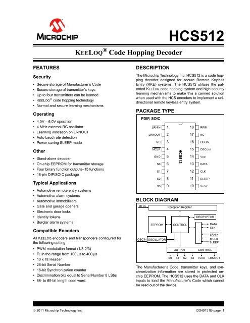
DESCRIPTION<br />
The <strong>Microchip</strong> Technology Inc. <strong>HCS512</strong> is a code hopping<br />
decoder designed for secure Remote Keyless<br />
Entry (RKE) systems. The <strong>HCS512</strong> utilizes the patented<br />
KEELOQ code hopping system and high security<br />
learning mechanisms to make this a canned solution<br />
when used with the HCS encoders to implement a unidirectional<br />
remote keyless entry system.<br />
PACKAGE TYPE<br />
PDIP, SOIC<br />
BLOCK DIAGRAM<br />
RFIN<br />
LRNIN<br />
LRNOUT<br />
NC<br />
MCLR<br />
GND<br />
S0<br />
S1<br />
S2<br />
S3<br />
EEPROM<br />
OSCIN OSCILLATOR<br />
1<br />
2<br />
3<br />
4<br />
5<br />
6<br />
7<br />
8<br />
9<br />
<strong>HCS512</strong><br />
The Manufacturer’s Code, transmitter keys, and synchronization<br />
information are stored in protected onchip<br />
EEPROM. The <strong>HCS512</strong> uses the DATA and CLK<br />
inputs to load the Manufacturer’s Code which cannot<br />
be read out of the device.<br />
18<br />
17<br />
16<br />
15<br />
14<br />
13<br />
12<br />
11<br />
Reception Register<br />
CONTROL<br />
OUTPUT<br />
10<br />
S0 S1 S2 S3<br />
RFIN<br />
NC<br />
OSCIN<br />
OSCOUT<br />
VDD<br />
DATA<br />
CLK<br />
SLEEP<br />
VLOW<br />
DECRYPTOR<br />
CONTROL<br />
VLOW<br />
DATA<br />
CLK<br />
LRNIN<br />
MCLR<br />
SLEEP<br />
LRNOUT<br />
© 2011 <strong>Microchip</strong> Technology Inc. DS40151E-page 1
<strong>HCS512</strong><br />
The <strong>HCS512</strong> operates over a wide voltage range of<br />
3.0 volts to 6.0 volts. The decoder employs automatic<br />
baud rate detection which allows it to compensate for<br />
wide variations in transmitter data rate. The decoder<br />
contains sophisticated error checking algorithms to<br />
ensure only valid codes are accepted.<br />
1.0 SYSTEM OVERVIEW<br />
Key Terms<br />
The following is a list of key terms used throughout this<br />
data sheet. For additional information on KEELOQ and<br />
Code <strong>Hopping</strong>, refer to Technical Brief 3 (TB003).<br />
• RKE - Remote Keyless Entry<br />
• Button Status - Indicates what button input(s)<br />
activated the transmission. Encompasses the 4<br />
button status bits S3, S2, S1 and S0 (Figure 8-2).<br />
• Code <strong>Hopping</strong> - A method by which a code,<br />
viewed externally to the system, appears to<br />
change unpredictably each time it is transmitted.<br />
• Code word - A block of data that is repeatedly<br />
transmitted upon button activation (Figure 8-1).<br />
• Transmission - A data stream consisting of<br />
repeating code words (Figure 8-1).<br />
• Crypt key - A unique and secret 64-bit number<br />
used to encrypt and decrypt data. In a symmetrical<br />
block cipher such as the KEELOQ algorithm,<br />
the encryption and decryption keys are equal and<br />
will therefore be referred to generally as the crypt<br />
key.<br />
• Encoder - A device that generates and encodes<br />
data.<br />
• Encryption Algorithm - A recipe whereby data is<br />
scrambled using a crypt key. The data can only be<br />
interpreted by the respective decryption algorithm<br />
using the same crypt key.<br />
• <strong>Decoder</strong> - A device that decodes data received<br />
from an encoder.<br />
• Decryption algorithm - A recipe whereby data<br />
scrambled by an encryption algorithm can be<br />
unscrambled using the same crypt key.<br />
• Learn – Learning involves the receiver calculating<br />
the transmitter’s appropriate crypt key, decrypting<br />
the received hopping code and storing the serial<br />
number, synchronization counter value and crypt<br />
key in EEPROM. The KEELOQ product family facilitates<br />
several learning strategies to be implemented<br />
on the decoder. The following are<br />
examples of what can be done.<br />
- Simple Learning<br />
The receiver uses a fixed crypt key, common<br />
to all components of all systems by the same<br />
manufacturer, to decrypt the received code<br />
word’s encrypted portion.<br />
- Normal Learning<br />
The receiver uses information transmitted<br />
during normal operation to derive the crypt<br />
key and decrypt the received code word’s<br />
encrypted portion.<br />
- Secure Learn<br />
The transmitter is activated through a special<br />
button combination to transmit a stored 60-bit<br />
seed value used to generate the transmitter’s<br />
crypt key. The receiver uses this seed value<br />
to derive the same crypt key and decrypt the<br />
received code word’s encrypted portion.<br />
• Manufacturer’s code – A unique and secret 64-<br />
bit number used to generate unique encoder crypt<br />
keys. Each encoder is programmed with a crypt<br />
key that is a function of the manufacturer’s code.<br />
Each decoder is programmed with the manufacturer<br />
code itself.<br />
1.1 HCS Encoder Overview<br />
The HCS encoders have a small EEPROM array which<br />
must be loaded with several parameters before use.<br />
The most important of these values are:<br />
• A crypt key that is generated at the time of production<br />
• A 16-bit synchronization counter value<br />
• A 28-bit serial number which is meant to be<br />
unique for every encoder<br />
The manufacturer programs the serial number for each<br />
encoder at the time of production, while the ‘Key Generation<br />
Algorithm’ generates the crypt key (Figure 1-1).<br />
Inputs to the key generation algorithm typically consist<br />
of the encoder’s serial number and a 64-bit manufacturer’s<br />
code, which the manufacturer creates.<br />
Note:<br />
The manufacturer code is a pivotal part of<br />
the system’s overall security. Consequently,<br />
all possible precautions must be<br />
taken and maintained for this code.<br />
DS40151E-page 2<br />
© 2011 <strong>Microchip</strong> Technology Inc.
<strong>HCS512</strong><br />
FIGURE 1-1:<br />
CREATION AND STORAGE OF CRYPT KEY DURING PRODUCTION<br />
Production<br />
Programmer<br />
Manufacturer’s<br />
Code<br />
Transmitter<br />
Serial Number<br />
Key<br />
Generation<br />
Algorithm<br />
Crypt<br />
Key<br />
<strong>HCS512</strong><br />
EEPROM Array<br />
Serial Number<br />
Crypt Key<br />
Sync Counter<br />
.<br />
.<br />
.<br />
The 16-bit synchronization counter is the basis behind<br />
the transmitted code word changing for each transmission;<br />
it increments each time a button is pressed. Due<br />
to the code hopping algorithm’s complexity, each increment<br />
of the synchronization value results in greater<br />
than 50% of the bits changing in the transmitted code<br />
word.<br />
Figure 1-2 shows how the key values in EEPROM are<br />
used in the encoder. Once the encoder detects a button<br />
press, it reads the button inputs and updates the synchronization<br />
counter. The synchronization counter and<br />
crypt key are input to the encryption algorithm and the<br />
output is 32 bits of encrypted information. This data will<br />
change with every button press, its value appearing<br />
externally to ‘randomly hop around’, hence it is referred<br />
to as the hopping portion of the code word. The 32-bit<br />
hopping code is combined with the button information<br />
and serial number to form the code word transmitted to<br />
the receiver. The code word format is explained in<br />
greater detail in Section 8.2.<br />
A receiver may use any type of controller as a decoder,<br />
but it is typically a microcontroller with compatible firmware<br />
that allows the decoder to operate in conjunction<br />
with an <strong>HCS512</strong> based transmitter. Section 5.0<br />
provides detail on integrating the <strong>HCS512</strong> into a system.<br />
A transmitter must first be ‘learned’ by the receiver<br />
before its use is allowed in the system. Learning<br />
includes calculating the transmitter’s appropriate crypt<br />
key, decrypting the received hopping code and storing<br />
the serial number, synchronization counter value and<br />
crypt key in EEPROM.<br />
In normal operation, each received message of valid<br />
format is evaluated. The serial number is used to determine<br />
if it is from a learned transmitter. If from a learned<br />
transmitter, the message is decrypted and the synchronization<br />
counter is verified. Finally, the button status is<br />
checked to see what operation is requested. Figure 1-3<br />
shows the relationship between some of the values<br />
stored by the receiver and the values received from<br />
the transmitter.<br />
FIGURE 1-2:<br />
BUILDING THE TRANSMITTED CODE WORD (ENCODER)<br />
EEPROM Array<br />
Crypt Key<br />
Sync Counter<br />
KEELOQ ®<br />
Encryption<br />
Algorithm<br />
Serial Number<br />
Button Press<br />
Information<br />
Serial Number<br />
32 Bits<br />
Encrypted Data<br />
Transmitted Information<br />
© 2011 <strong>Microchip</strong> Technology Inc. DS40151E-page 3
<strong>HCS512</strong><br />
FIGURE 1-3:<br />
BASIC OPERATION OF RECEIVER (DECODER)<br />
1<br />
Received Information<br />
EEPROM Array<br />
Button Press<br />
Information<br />
Serial Number<br />
32 Bits of<br />
Encrypted Data<br />
Manufacturer Code<br />
2<br />
Check for<br />
Match<br />
Serial Number<br />
Sync Counter<br />
Crypt Key<br />
3<br />
KEELOQ ®<br />
Decryption<br />
Algorithm<br />
Perform Function<br />
5<br />
Indicated by<br />
button press<br />
Decrypted<br />
Synchronization<br />
Counter<br />
4<br />
Check for<br />
Match<br />
NOTE: Circled numbers indicate the order of execution.<br />
2.0 PIN ASSIGNMENT<br />
PIN<br />
<strong>Decoder</strong><br />
I/O (1) Buffer<br />
Function<br />
Type (1)<br />
Description<br />
1 LRNIN I TTL Learn input - initiates learning, 10K pull-up required on input<br />
2 LRNOUT O TTL Learn output - indicates learning<br />
3 NC — TTL Do not connect<br />
4 MCLR I ST Master clear input<br />
5 Ground P — Ground connection<br />
6 S0 O TTL Switch 0<br />
7 S1 O TTL Switch 1<br />
8 S2 O TTL Switch 2<br />
9 S3 O TTL Switch 3<br />
10 VLOW O TTL Battery low indication output<br />
11 SLEEP I TTL Connect to RFIN to allow wake-up from SLEEP<br />
12 CLK I/O TTL/ST (2) Clock in Programming mode and Synchronous mode<br />
13 DATA I/O TTL/ST (2) Data in Programming mode and Synchronous mode<br />
14 VDD P — Power connection<br />
15 OSCOUT (1MHZ) O TTL Oscillator out (test point)<br />
16 OSCIN (4MHz) I ST Oscillator in – recommended values 4.7 kΩ and 22 pF<br />
17 NC — —<br />
18 RFIN I TTL RF input from receiver<br />
Note 1: P = power, I = in, O = out, and ST = Schmitt Trigger input.<br />
2: Pin 12 and Pin 13 have a dual purpose. After RESET, these pins are used to determine if Programming<br />
mode is selected in which case they are the clock and data lines. In normal operation, they are the clock<br />
and data lines of the synchronous data output stream.<br />
DS40151E-page 4<br />
© 2011 <strong>Microchip</strong> Technology Inc.
<strong>HCS512</strong><br />
3.0 DESCRIPTION OF FUNCTIONS<br />
3.1 Parallel Interface<br />
The <strong>HCS512</strong> activates the S3, S2, S1 & S0 outputs<br />
when a new valid code is received. The outputs will be<br />
activated for approximately 500 ms. If a repeated code<br />
is received during this time, the output extends for<br />
approximately 500 ms.<br />
3.2 Serial Interface<br />
The decoder has a PWM/Synchronous interface connection<br />
to microcontrollers with limited I/O. An output<br />
data stream is generated when a valid transmission is<br />
received. The data stream consists of one START bit,<br />
four function bits, one bit for battery status, one bit to<br />
indicate a repeated transmission, two status bits, and<br />
one STOP bit. (Table 3-1). The DATA and CLK lines are<br />
used to send a synchronous event message.<br />
A special status message is transmitted on the second<br />
pass of learn. This allows the controlling microcontroller<br />
to determine if the learn was successful (Result<br />
= 1) and if a previous transmitter was overwritten<br />
(Overwrite = 1). The status message is shown in<br />
Figure 3-2.<br />
Table 3-1 show the values for TX1:0 and the number of<br />
transmitters learned.<br />
TABLE 3-1:<br />
STATUS BITS<br />
TX1 TX0 Number of Transmitters<br />
0 0 One<br />
0 1 Two<br />
1 0 Three<br />
1 1 Four<br />
FIGURE 3-1:<br />
DATA OUTPUT FORMAT<br />
START S3 S2 S1 S0 VLOW REPEAT TX1 TX0 STOP<br />
FIGURE 3-2:<br />
STATUS MESSAGE FORMAT<br />
START 0 0 0 0 RESULT OVRWR TX1 TX0 STOP<br />
A 1-wire PWM or 2-wire synchronous interface can be used.<br />
In 1-wire mode, the data is transmitted as a PWM signal with a basic pulse width of 400 μs.<br />
In 2-wire mode, Synchronous mode PWM bits start on the rising edge of the clock, and the bits must be sampled on the<br />
falling edge. The START bit is a ‘1’ and the STOP bit is ‘0’.<br />
FIGURE 3-2: PWM OUTPUT FORMAT (1)<br />
LOGIC “1”<br />
1/31/3 1/3<br />
LOGIC “0”<br />
600 μs<br />
1200 μs<br />
CLK<br />
DATA<br />
START S3 S2 S1 S0 VLOW RPT Reserved Reserved STOP<br />
1200 μs<br />
Note: The <strong>Decoder</strong> output PWM format logic (“1” / “0”) is reversed with respect of the Encoder modulation format.<br />
© 2011 <strong>Microchip</strong> Technology Inc. DS40151E-page 5
<strong>HCS512</strong><br />
4.0 DECODER OPERATION<br />
4.1 Learning a Transmitter to a<br />
Receiver<br />
Either the serial number-based learning method or the<br />
seed-based learning method can be selected. The<br />
learning method is selected in the configuration byte. In<br />
order for a transmitter to be used with a decoder, the<br />
transmitter must first be ‘learned’. When a transmitter is<br />
learned to a decoder, the decoder stores the crypt key,<br />
a check value of the serial number and current synchronization<br />
value in EEPROM. The decoder must<br />
keep track of these values for every transmitter that is<br />
learned. The maximum number of transmitters that can<br />
be learned is four. The decoder must also contain the<br />
Manufacturer’s Code in order to learn a transmitter.<br />
The Manufacturer’s Code will typically be the same for<br />
all decoders in a system.<br />
The <strong>HCS512</strong> has four memory slots. After an “erase all”<br />
procedure, all the memory slots will be cleared. Erase<br />
all is activated by taking LRNIN low for approximately<br />
10 seconds. When a new transmitter is learned, the<br />
decoder searches for an empty memory slot and stores<br />
the transmitter’s information in that memory slot. When<br />
all memory slots are full, the decoder randomly overwrites<br />
existing transmitters.<br />
4.1.1 LEARNING PROCEDURE<br />
Learning is activated by taking the LRNIN input low for<br />
longer than 64 ms. This input requires an external pullup<br />
resistor.<br />
To learn a new transmitter to the <strong>HCS512</strong> decoder, the<br />
following sequence is required:<br />
1. Enter Learning mode by pulling LRNIN low for<br />
longer than 64 ms. The LRNOUT output will go<br />
high.<br />
2. Activate the transmitter until the LRNOUT output<br />
goes low indicating reception of a valid code<br />
(hopping message).<br />
3. Activate the transmitter a second time until the<br />
LRNOUT toggles for 4 seconds (in Secure<br />
Learning mode, the seed transmission must be<br />
transmitted during the second stage of learn by<br />
activating the appropriate buttons on the transmitter).<br />
If LRNIN is taken low momentarily during the<br />
learn status indication, the indication will be terminated.<br />
Once a successful learning sequence<br />
is detected, the indication can be terminated<br />
allowing quick learning in a manufacturing<br />
setup.<br />
4. The transmitter is now learned into the decoder.<br />
5. Repeat steps 1-4 to learn up to four transmitters.<br />
6. Learning will be terminated if two non-sequential<br />
codes were received or if two acceptable codes<br />
were not decoded within 30 seconds.<br />
The following checks are performed on the decoder to<br />
determine if the transmission is valid during learn:<br />
• The first code word is checked for bit integrity.<br />
• The second code word is checked for bit integrity.<br />
• The hopping code is decrypted.<br />
• If all the checks pass, the serial number and synchronization<br />
counters are stored in EEPROM<br />
memory.<br />
Figure 4-1 shows a flow chart of the learn sequence.<br />
FIGURE 4-1:<br />
Enter Learn<br />
Mode<br />
Wait for Reception<br />
of a Valid Code<br />
Wait for Reception<br />
of Second<br />
Non-Repeated<br />
Valid Code<br />
Generate Key<br />
from Serial Number<br />
or Seed Value<br />
Use Generated Key<br />
to Decrypt<br />
LEARN SEQUENCE<br />
Compare Discrimination<br />
Value with Serial Number<br />
Equal<br />
?<br />
Learn successful. Store:<br />
Serial number check value<br />
Synchronization counter<br />
crypt key<br />
Exit<br />
Yes<br />
No<br />
Learn<br />
Unsuccessful<br />
DS40151E-page 6<br />
© 2011 <strong>Microchip</strong> Technology Inc.
<strong>HCS512</strong><br />
4.2 Validation of Codes<br />
The decoder waits for a transmission and checks the<br />
serial number to determine if the transmitter has been<br />
learned. If learned, the decoder decrypts the encrypted<br />
portion of the transmission using the crypt key. It uses<br />
the discrimination bits to determine if the decryption<br />
was valid. If everything up to this point is valid, the<br />
synchronization value is evaluated.<br />
4.3 Validation Steps<br />
Validation consists of the following steps:<br />
• Search EEPROM to find the Serial Number<br />
Check Value Match<br />
• Decrypt the <strong>Hopping</strong> Code<br />
• Compare the 10 bits of discrimination value with<br />
the lower 10 bits of serial number<br />
• Check if the synchronization counter falls within<br />
the first synchronization window.<br />
• Check if the synchronization counter falls within<br />
the second synchronization window.<br />
• If a valid transmission is found, update the synchronization<br />
counter, else use the next transmitter<br />
block and repeat the tests.<br />
FIGURE 4-2:<br />
No<br />
DECODER OPERATION<br />
Start<br />
Transmission<br />
Received<br />
?<br />
Yes<br />
No Does<br />
Ser # Check Val<br />
Match<br />
?<br />
Yes<br />
Decrypt Transmission<br />
No<br />
No<br />
Is<br />
Decryption<br />
Valid<br />
?<br />
Yes<br />
Is<br />
Counter<br />
Within 16<br />
?<br />
No<br />
Is<br />
Counter<br />
Within 32K<br />
?<br />
Yes<br />
Execute<br />
Command<br />
and<br />
Update<br />
Counter<br />
Yes<br />
Save Counter<br />
in Temp Location<br />
© 2011 <strong>Microchip</strong> Technology Inc. DS40151E-page 7
<strong>HCS512</strong><br />
4.4 Synchronization with <strong>Decoder</strong><br />
(Evaluating the Counter)<br />
The KEELOQ technology patent scope includes a<br />
sophisticated synchronization technique that does not<br />
require the calculation and storage of future codes. The<br />
technique securely blocks invalid transmissions while<br />
providing transparent resynchronization to transmitters<br />
inadvertently activated away from the receiver.<br />
Figure 4-3 shows a 3-partition, rotating synchronization<br />
window. The size of each window is optional but the<br />
technique is fundamental. Each time a transmission is<br />
authenticated, the intended function is executed and<br />
the transmission's synchronization counter value is<br />
stored in EEPROM. From the currently stored counter<br />
value there is an initial "Single Operation" forward window<br />
of 16 codes. If the difference between a received<br />
synchronization counter and the last stored counter is<br />
within 16, the intended function will be executed on the<br />
single button press and the new synchronization counter<br />
will be stored. Storing the new synchronization<br />
counter value effectively rotates the entire synchronization<br />
window.<br />
A "Double Operation" (resynchronization) window further<br />
exists from the Single Operation window up to 32K<br />
codes forward of the currently stored counter value. It<br />
is referred to as "Double Operation" because a transmission<br />
with synchronization counter value in this window<br />
will require an additional, sequential counter<br />
transmission prior to executing the intended function.<br />
Upon receiving the sequential transmission the<br />
decoder executes the intended function and stores the<br />
synchronization counter value. This resynchronization<br />
occurs transparently to the user as it is human nature<br />
to press the button a second time if the first was unsuccessful.<br />
The third window is a "Blocked Window" ranging from<br />
the double operation window to the currently stored<br />
synchronization counter value. Any transmission with<br />
synchronization counter value within this window will<br />
be ignored. This window excludes previously used,<br />
perhaps code-grabbed transmissions from accessing<br />
the system.<br />
Note:<br />
The synchronization method described in<br />
this section is only a typical implementation<br />
and because it is usually implemented in<br />
firmware, it can be altered to fit the needs<br />
of a particular system.<br />
FIGURE 4-3:<br />
SYNCHRONIZATION WINDOW<br />
Entire Window<br />
rotates to eliminate<br />
use of previously<br />
used codes<br />
Blocked<br />
Window<br />
(32K Codes)<br />
Double Operation<br />
(resynchronization)<br />
Window<br />
(32K Codes)<br />
Stored<br />
Synchronization<br />
Counter Value<br />
Single Operation<br />
Window<br />
(16 Codes)<br />
4.5 SLEEP Mode<br />
The SLEEP mode of the <strong>HCS512</strong> is used to reduce<br />
current consumption when no RF input signal is present.<br />
SLEEP mode will only be effective in systems<br />
where the RF receiver is relatively quiet when no signal<br />
is present. During SLEEP, the clock stops, thereby significantly<br />
reducing the operating current. SLEEP mode<br />
is enabled by the SLEEP bit in the configuration byte.<br />
The <strong>HCS512</strong> will enter SLEEP mode when:<br />
• The RF line is low<br />
• After a function output is switched off<br />
• Learn mode is terminated (time-out reached)<br />
The device will not enter SLEEP mode when:<br />
• A function output is active<br />
• Learn sequence active<br />
• Device is in Programming mode<br />
The device will wake-up from SLEEP when:<br />
• The SLEEP input pin changes state<br />
• The CLOCK line changes state<br />
Note:<br />
During SLEEP mode the CLK line will<br />
change from an output line to an input line<br />
that can be used to wake-up the device.<br />
Connect CLK to LRNIN via a 100K resistor<br />
to reliably enter the Learn mode whenever<br />
SLEEP mode is active.<br />
DS40151E-page 8<br />
© 2011 <strong>Microchip</strong> Technology Inc.
<strong>HCS512</strong><br />
5.0 INTEGRATING THE <strong>HCS512</strong><br />
INTO A SYSTEM<br />
The <strong>HCS512</strong> can act as a stand-alone decoder or be<br />
interfaced to a microcontroller. Typical stand-alone<br />
applications include garage door openers and electronic<br />
door locks. In stand-alone applications, the<br />
<strong>HCS512</strong> will handle learning, reception, decryption,<br />
and validation of the received code; and generate the<br />
appropriate output. For a garage door opener, the<br />
<strong>HCS512</strong> input will be connected to an RF receiver, and<br />
the output, to a relay driver to connect a motor controller.<br />
Typical systems where the <strong>HCS512</strong> will be connected<br />
to a microcontroller include vehicle and home security<br />
systems. The <strong>HCS512</strong> input will be connected to an RF<br />
receiver and the function outputs to the microcontroller.<br />
The <strong>HCS512</strong> will handle all the decoding functions and<br />
the microcontroller, all the system functions. The Serial<br />
Output mode with a 1- or 2-wire interface can be used<br />
if the microcontroller is I/O limited.<br />
6.0 DECODER PROGRAMMING<br />
The PG306001 production programmer will allow easy<br />
setup and programming of the configuration byte and<br />
the manufacturer’s code.<br />
6.1 Configuration Byte<br />
The configuration byte is used to set system configuration<br />
for the decoder. The LRN bits determine which<br />
algorithm (Decrypt or XOR) is used for the key generation.<br />
SC_LRN determines whether normal learn (key<br />
derived from serial number) or secure learn (key<br />
derived from seed value) is used.<br />
TABLE 6-1:<br />
CONFIGURATION BYTE<br />
Bit Name Description<br />
0 LRN0 Learn algorithm select<br />
1 LRN1 Not used<br />
2 SC_LRN Secure Learn enable (1 = enabled)<br />
3 SLEEP SLEEP enable (1 = enabled)<br />
4 RES1 Not used<br />
5 RES2 Not used<br />
6 RES3 Not used<br />
7 RES4 Not used<br />
TABLE 6-2:<br />
LEARN METHOD LRN0, LRN1<br />
DEFINITIONS<br />
LRN0<br />
Description<br />
0 Decrypt algorithm<br />
1 XOR algorithm<br />
© 2011 <strong>Microchip</strong> Technology Inc. DS40151E-page 9
<strong>HCS512</strong><br />
6.2 Programming the Manufacturer’s<br />
Code<br />
The manufacturer’s code must be programmed into<br />
EEPROM memory through the synchronous programming<br />
interface using the DATA and CLK lines. Provision<br />
must be made for connections to these pins if the<br />
decoder is going to be programmed in circuit.<br />
Programming mode is activated if the CLK is low for at<br />
least 1 ms and then goes high within 64 ms after powerup,<br />
stays high for longer than 8 ms but not longer than<br />
128 ms. After entering Programming mode the 64-bit<br />
manufacturer’s code, 8-bit configuration byte, and 8-bit<br />
checksum is sent to the device using the synchronous<br />
interface. After receiving the 80-bit message the checksum<br />
is verified and the information is written to<br />
EEPROM. If the programming operation was successful,<br />
the <strong>HCS512</strong> will respond with an Acknowledge<br />
pulse.<br />
After programming the manufacturer’s code, the<br />
<strong>HCS512</strong> decoder will automatically activate an<br />
Erase All function, removing all transmitters from the<br />
system.<br />
6.3 Download Format<br />
The manufacturer’s code and configuration byte must<br />
be downloaded Least Significant Byte, Least Significant<br />
bit first as shown in Table 6-3.<br />
6.4 Checksum<br />
The checksum is used by the <strong>HCS512</strong> to check that the<br />
data downloaded was correctly received before programming<br />
the data. The checksum is calculated so that<br />
the 10 bytes added together (discarding the overflow<br />
bits) is zero. The checksum can be calculated by adding<br />
the first 9 bytes of data together and subtracting the<br />
result from zero. Throughout the calculation the overflow<br />
is discarded.<br />
Given a manufacturer’s code of 01234567-<br />
89ABCDEF 16 and a Configuration Word of 1 16 , the<br />
checksum is calculated as shown in Figure 6-1. The<br />
checksum is 3F 16 .<br />
6.5 Test Transmitter<br />
The <strong>HCS512</strong> decoder will automatically add a test<br />
transmitter each time an Erase All Function is done. A<br />
test transmitter is defined as a transmitter with a serial<br />
number of zero. After an Erase All, the test transmitter<br />
will always work without learning and will not check the<br />
synchronization counter of the transmitter. Learning of<br />
any new transmitters will erase the test transmitter.<br />
Note 1: A transmitter with a serial number of zero<br />
cannot be learned. Learn will fail after the<br />
first transmission.<br />
2: Always learn at least one transmitter after<br />
an Erase All sequence. This ensures that<br />
the test transmitter is erased.<br />
TABLE 6-3:<br />
DOWNLOAD DATA<br />
Byte 9 Byte 8 Byte 7 Byte 6 Byte 5 Byte 4 Byte 3 Byte 2 Byte 1 Byte 0<br />
Checksum<br />
Config<br />
Man<br />
Key_7<br />
Man<br />
Key_6<br />
Man<br />
Key_5<br />
Man<br />
Key_4<br />
Man<br />
Key_3<br />
Man<br />
Key_2<br />
Man<br />
Key_1<br />
Man<br />
Key_0<br />
Byte 0, right-most bit downloaded first.<br />
FIGURE 6-1:<br />
CHECKSUM CALCULATION<br />
01 16 + 23 16 = 24 6<br />
24 16 + 45 16 = 69 16<br />
69 16 + 67 16 = D0 16<br />
D0 16 + 89 16 = 159 16<br />
59 16 + AB 16 = 104 16 (Carry is discarded)<br />
04 16 + CD 16 = D1 16 (Carry is discarded)<br />
D1 16 + EF 16 = 1C0 16<br />
C0 16 + 1 16 = C1 16 (Carry is discarded)<br />
(FF 16 - C1 16 ) + 1 16 = 3F 16<br />
DS40151E-page 10<br />
© 2011 <strong>Microchip</strong> Technology Inc.
<strong>HCS512</strong><br />
FIGURE 6-2:<br />
PROGRAMMING WAVEFORMS<br />
MCLR<br />
T CKL<br />
T PS T PH1 TPH2<br />
T CKH<br />
T ACK<br />
T ACKH<br />
CLK<br />
(Clock)<br />
DAT<br />
(Data)<br />
Bit0 Bit1<br />
Bit78 Bit79 Ack<br />
Enter Program Mode<br />
80-bit Data Package<br />
Acknowledge<br />
pulse<br />
TABLE 6-4:<br />
PROGRAMMING TIMING REQUIREMENTS<br />
Parameter Symbol Min. Max. Units<br />
Program mode setup time TPS 1 64 ms<br />
Hold time 1 TPH1 8 128 ms<br />
Hold time 2 TPH2 0.05 320 ms<br />
Clock High Time TCKH 0.05 320 ms<br />
Clock Low Time TCKL 0.050 320 ms<br />
Acknowledge Time TACK — 80 ms<br />
Acknowledge duration TACKH 1 — ms<br />
Note: FOSC equals 4 MHz.<br />
© 2011 <strong>Microchip</strong> Technology Inc. DS40151E-page 11
<strong>HCS512</strong><br />
7.0 KEY GENERATION SCHEMES<br />
The <strong>HCS512</strong> decoder has two key generation schemes. Normal learning uses the transmitter’s serial number to derive<br />
two input seeds which are used as inputs to the key generation algorithm. Secure learning uses the seed transmission<br />
to derive the two input seeds. Two key generation algorithms are available to convert the inputs seeds to secret keys.<br />
The appropriate scheme is selected in the Configuration Word.<br />
FIGURE 7-1:<br />
Serial<br />
Number<br />
Patched<br />
Manufacturer’s<br />
Key<br />
Key Generation<br />
Algorithms<br />
-------------------<br />
Decrypt<br />
XOR<br />
Encoder<br />
Key<br />
Seed<br />
7.1 Normal Learning (Serial Number Derived)<br />
The two input seeds are composed from the serial number in two ways, depending on the encoder type. The encoder<br />
type is determined from the number of bits in the incoming transmission. SourceH is used to calculate the upper 32 bits<br />
of the crypt key, and SourceL, for the lower 32 bits.<br />
For 28-bit serial number encoders (66 / 67-bit transmissions):<br />
SourceH = 6H + 28 bit Serial Number<br />
SourceL = 2H + 28 bit Serial Number<br />
7.2 Secure Learning (Seed Derived)<br />
The two input seeds are composed from the seed value that is transmitted during secure learning. The lower 32 bits of<br />
the seed transmission is used to compose the lower seed, and the upper 32 bits, for the upper seed. The upper 4 bits<br />
(function code) are set to zero.<br />
For 32-bit seed encoders:<br />
SourceH = Serial Number Lower 28 bits (with upper 4 bits always zero)<br />
SourceL = Seed 32 bits<br />
For 48-bit seed encoders:<br />
SourceH = Seed Upper 16 bits + Serial Number Upper 16 bits (with upper 4 bits always zero)
<strong>HCS512</strong><br />
7.3 Key Generation Algorithms<br />
There are two key generation algorithms implemented in the <strong>HCS512</strong> decoder. The KEELOQ decryption algorithm provides<br />
a higher level of security than the XOR algorithm. Section 6.1 describes the selection of the algorithms in the configuration<br />
byte.<br />
7.3.1 KEELOQ DECRYPT ALGORITHM<br />
This algorithm uses the KEELOQ decryption algorithm and the manufacturer’s code to derive the crypt key as follows:<br />
Key Upper 32 bits = Decrypt (SourceH) 64 Bit Manufacturers Code<br />
Key Lower 32 bits = Decrypt (SourceL) 64 Bit Manufacturers Code<br />
7.3.2 XOR WITH THE MANUFACTURER’S CODE<br />
The two 32-bits seeds are XOR with the manufacturer’s code to form the 64 bit crypt key.<br />
Key Upper 32 bits = SourceH XOR Manufacturers Code Upper 32 bits<br />
Key Lower 32 bits = SourceL XOR Manufacturers Code Lower 32 bits<br />
After programming the manufacturer’s code, the <strong>HCS512</strong> decoder will automatically activate an Erase All function,<br />
removing all transmitters from the system.<br />
If LRNIN is taken low momentarily during the learn status indication, the indication will be terminated. Once a successful<br />
learning sequence is detected, the indication can be terminated, allowing quick learning in a manufacturing setup.<br />
FIGURE 7-2:<br />
<strong>HCS512</strong> KEY GENERATION<br />
Normal Learn (SC_LRN = 0)<br />
LRN0 = 0<br />
Padding<br />
2<br />
Padding<br />
6<br />
28-bit Serial Number<br />
28-bit Serial Number<br />
KEELOQ ®<br />
Decryption<br />
Algorithm<br />
LS 32 bits of crypt key<br />
MS 32 bits of crypt key<br />
Secure Learn (SC_LRN = 1)<br />
LRN0 = 0<br />
Padding<br />
0000b<br />
LS 32 bits of Seed Transmission<br />
MS 28 bits of Seed Transmission<br />
KEELOQ<br />
Decryption<br />
Algorithm<br />
LS 32 bits of crypt key<br />
MS 32 bits of crypt key<br />
Secure Learn XOR (SC_LRN = 1)<br />
LRN0 = 1<br />
Padding<br />
0000b<br />
LS 32 bits of Seed Transmission<br />
MS 28 bits of Seed Transmission<br />
XOR<br />
LS 32 bits of crypt key<br />
MS 32 bits of crypt key<br />
© 2011 <strong>Microchip</strong> Technology Inc. DS40151E-page 13
<strong>HCS512</strong><br />
8.0 KEELOQ ENCODERS<br />
8.1 Transmission Format (PWM)<br />
The KEELOQ encoder transmission is made up of several<br />
parts (Figure 8-1). Each transmission begins with<br />
a preamble and a header, followed by the encrypted<br />
and then the fixed data. The actual data is 66/69 bits<br />
which consists of 32 bits of encrypted data and 34/37<br />
bits of non-encrypted data. Each transmission is followed<br />
by a guard period before another transmission<br />
can begin. The encrypted portion provides up to four<br />
billion changing code combinations and includes the<br />
button status bits (based on which buttons were activated)<br />
along with the synchronization counter value<br />
and some discrimination bits. The non-encrypted portion<br />
is comprised of the status bits, the function bits,<br />
and the 28-bit serial number. The encrypted and nonencrypted<br />
combined sections increase the number of<br />
combinations to 7.38 x 10 19 .<br />
8.2 Code Word Organization<br />
The HCSXXX encoder transmits a 66/69-bit code word<br />
when a button is pressed. The 66/69-bit word is constructed<br />
from an encryption portion and a nonencrypted<br />
code portion (Figure 8-2).<br />
The Encrypted Data is generated from four button bits,<br />
two overflow counter bits, ten discrimination bits, and<br />
the 16-bit synchronization value.<br />
The Non-encrypted Data is made up from 2 status<br />
bits, 4 function bits, and the 28/32-bit serial number.<br />
FIGURE 8-1:<br />
TRANSMISSION FORMAT (PWM)<br />
TE TE TE<br />
LOGIC "0"<br />
LOGIC "1"<br />
TBP<br />
50% Preamble<br />
10xTE Encrypted<br />
Header Portion<br />
Fixed Code<br />
Portion<br />
Guard<br />
Time<br />
FIGURE 8-2:<br />
CODE WORD ORGANIZATION<br />
34 bits of Fixed Portion 32 bits of Encrypted Portion<br />
MSb<br />
Repeat<br />
(1-bit)<br />
VLOW<br />
(1-bit)<br />
Button<br />
Status<br />
S2 S1 S0 S3<br />
Serial Number<br />
(28 bits)<br />
Button<br />
Status<br />
S2 S1 S0 S3<br />
OVR<br />
(2 bits)<br />
DISC<br />
(10 bits)<br />
Sync Counter<br />
(16 bits)<br />
66 Data bits<br />
Transmitted<br />
LSb first.<br />
LSb<br />
MSb<br />
Repeat<br />
(1-bit)<br />
VLOW<br />
(1-bit)<br />
Button<br />
Status<br />
1 1 1 1<br />
Serial Number<br />
(28 bits)<br />
SEED<br />
(32 bits)<br />
SEED replaces Encrypted Portion when all button inputs are activated at the same time.<br />
LSb<br />
DS40151E-page 14<br />
© 2011 <strong>Microchip</strong> Technology Inc.
<strong>HCS512</strong><br />
9.0 DEVELOPMENT SUPPORT<br />
The PIC ® microcontrollers and dsPIC ® digital signal<br />
controllers are supported with a full range of software<br />
and hardware development tools:<br />
• Integrated Development Environment<br />
- MPLAB ® IDE Software<br />
• Compilers/Assemblers/Linkers<br />
- MPLAB C Compiler for Various Device<br />
Families<br />
- HI-TECH C for Various Device Families<br />
- MPASM TM Assembler<br />
- MPLINK TM Object Linker/<br />
MPLIB TM Object Librarian<br />
- MPLAB Assembler/Linker/Librarian for<br />
Various Device Families<br />
• Simulators<br />
- MPLAB SIM Software Simulator<br />
• Emulators<br />
- MPLAB REAL ICE In-Circuit Emulator<br />
• In-Circuit Debuggers<br />
- MPLAB ICD 3<br />
- PICkit 3 Debug Express<br />
• Device Programmers<br />
- PICkit 2 Programmer<br />
- MPLAB PM3 Device Programmer<br />
• Low-Cost Demonstration/Development Boards,<br />
Evaluation Kits, and Starter Kits<br />
9.1 MPLAB Integrated Development<br />
Environment Software<br />
The MPLAB IDE software brings an ease of software<br />
development previously unseen in the 8/16/32-bit<br />
microcontroller market. The MPLAB IDE is a Windows ®<br />
operating system-based application that contains:<br />
• A single graphical interface to all debugging tools<br />
- Simulator<br />
- Programmer (sold separately)<br />
- In-Circuit Emulator (sold separately)<br />
- In-Circuit Debugger (sold separately)<br />
• A full-featured editor with color-coded context<br />
• A multiple project manager<br />
• Customizable data windows with direct edit of<br />
contents<br />
• High-level source code debugging<br />
• Mouse over variable inspection<br />
• Drag and drop variables from source to watch<br />
windows<br />
• Extensive on-line help<br />
• Integration of select third party tools, such as<br />
IAR C Compilers<br />
The MPLAB IDE allows you to:<br />
• Edit your source files (either C or assembly)<br />
• One-touch compile or assemble, and download to<br />
emulator and simulator tools (automatically<br />
updates all project information)<br />
• Debug using:<br />
- Source files (C or assembly)<br />
- Mixed C and assembly<br />
- Machine code<br />
MPLAB IDE supports multiple debugging tools in a<br />
single development paradigm, from the cost-effective<br />
simulators, through low-cost in-circuit debuggers, to<br />
full-featured emulators. This eliminates the learning<br />
curve when upgrading to tools with increased flexibility<br />
and power.<br />
© 2011 <strong>Microchip</strong> Technology Inc. DS40151E-page 15
<strong>HCS512</strong><br />
9.2 MPLAB C Compilers for Various<br />
Device Families<br />
The MPLAB C Compiler code development systems<br />
are complete ANSI C compilers for <strong>Microchip</strong>’s PIC18,<br />
PIC24 and PIC32 families of microcontrollers and the<br />
dsPIC30 and dsPIC33 families of digital signal controllers.<br />
These compilers provide powerful integration<br />
capabilities, superior code optimization and ease of<br />
use.<br />
For easy source level debugging, the compilers provide<br />
symbol information that is optimized to the MPLAB IDE<br />
debugger.<br />
9.3 HI-TECH C for Various Device<br />
Families<br />
The HI-TECH C Compiler code development systems<br />
are complete ANSI C compilers for <strong>Microchip</strong>’s PIC<br />
family of microcontrollers and the dsPIC family of digital<br />
signal controllers. These compilers provide powerful<br />
integration capabilities, omniscient code generation<br />
and ease of use.<br />
For easy source level debugging, the compilers provide<br />
symbol information that is optimized to the MPLAB IDE<br />
debugger.<br />
The compilers include a macro assembler, linker, preprocessor,<br />
and one-step driver, and can run on multiple<br />
platforms.<br />
9.4 MPASM Assembler<br />
The MPASM Assembler is a full-featured, universal<br />
macro assembler for PIC10/12/16/18 MCUs.<br />
The MPASM Assembler generates relocatable object<br />
files for the MPLINK Object Linker, Intel ® standard HEX<br />
files, MAP files to detail memory usage and symbol<br />
reference, absolute LST files that contain source lines<br />
and generated machine code and COFF files for<br />
debugging.<br />
The MPASM Assembler features include:<br />
• Integration into MPLAB IDE projects<br />
• User-defined macros to streamline<br />
assembly code<br />
• Conditional assembly for multi-purpose<br />
source files<br />
• Directives that allow complete control over the<br />
assembly process<br />
9.5 MPLINK Object Linker/<br />
MPLIB Object Librarian<br />
The MPLINK Object Linker combines relocatable<br />
objects created by the MPASM Assembler and the<br />
MPLAB C18 C Compiler. It can link relocatable objects<br />
from precompiled libraries, using directives from a<br />
linker script.<br />
The MPLIB Object Librarian manages the creation and<br />
modification of library files of precompiled code. When<br />
a routine from a library is called from a source file, only<br />
the modules that contain that routine will be linked in<br />
with the application. This allows large libraries to be<br />
used efficiently in many different applications.<br />
The object linker/library features include:<br />
• Efficient linking of single libraries instead of many<br />
smaller files<br />
• Enhanced code maintainability by grouping<br />
related modules together<br />
• Flexible creation of libraries with easy module<br />
listing, replacement, deletion and extraction<br />
9.6 MPLAB Assembler, Linker and<br />
Librarian for Various Device<br />
Families<br />
MPLAB Assembler produces relocatable machine<br />
code from symbolic assembly language for PIC24,<br />
PIC32 and dsPIC devices. MPLAB C Compiler uses<br />
the assembler to produce its object file. The assembler<br />
generates relocatable object files that can then be<br />
archived or linked with other relocatable object files and<br />
archives to create an executable file. Notable features<br />
of the assembler include:<br />
• Support for the entire device instruction set<br />
• Support for fixed-point and floating-point data<br />
• Command line interface<br />
• Rich directive set<br />
• Flexible macro language<br />
• MPLAB IDE compatibility<br />
DS40151E-page 16<br />
© 2011 <strong>Microchip</strong> Technology Inc.
<strong>HCS512</strong><br />
9.7 MPLAB SIM Software Simulator<br />
The MPLAB SIM Software Simulator allows code<br />
development in a PC-hosted environment by simulating<br />
the PIC ® MCUs and dsPIC ® DSCs on an instruction<br />
level. On any given instruction, the data areas can be<br />
examined or modified and stimuli can be applied from<br />
a comprehensive stimulus controller. Registers can be<br />
logged to files for further run-time analysis. The trace<br />
buffer and logic analyzer display extend the power of<br />
the simulator to record and track program execution,<br />
actions on I/O, most peripherals and internal registers.<br />
The MPLAB SIM Software Simulator fully supports<br />
symbolic debugging using the MPLAB C Compilers,<br />
and the MPASM and MPLAB Assemblers. The software<br />
simulator offers the flexibility to develop and<br />
debug code outside of the hardware laboratory environment,<br />
making it an excellent, economical software<br />
development tool.<br />
9.8 MPLAB REAL ICE In-Circuit<br />
Emulator System<br />
MPLAB REAL ICE In-Circuit Emulator System is<br />
<strong>Microchip</strong>’s next generation high-speed emulator for<br />
<strong>Microchip</strong> Flash DSC and MCU devices. It debugs and<br />
programs PIC ® Flash MCUs and dsPIC ® Flash DSCs<br />
with the easy-to-use, powerful graphical user interface of<br />
the MPLAB Integrated Development Environment (IDE),<br />
included with each kit.<br />
The emulator is connected to the design engineer’s PC<br />
using a high-speed USB 2.0 interface and is connected<br />
to the target with either a connector compatible with incircuit<br />
debugger systems (RJ11) or with the new highspeed,<br />
noise tolerant, Low-Voltage Differential Signal<br />
(LVDS) interconnection (CAT5).<br />
The emulator is field upgradable through future firmware<br />
downloads in MPLAB IDE. In upcoming releases of<br />
MPLAB IDE, new devices will be supported, and new<br />
features will be added. MPLAB REAL ICE offers<br />
significant advantages over competitive emulators<br />
including low-cost, full-speed emulation, run-time<br />
variable watches, trace analysis, complex breakpoints, a<br />
ruggedized probe interface and long (up to three meters)<br />
interconnection cables.<br />
9.9 MPLAB ICD 3 In-Circuit Debugger<br />
System<br />
MPLAB ICD 3 In-Circuit Debugger System is <strong>Microchip</strong>'s<br />
most cost effective high-speed hardware<br />
debugger/programmer for <strong>Microchip</strong> Flash Digital Signal<br />
Controller (DSC) and microcontroller (MCU)<br />
devices. It debugs and programs PIC ® Flash microcontrollers<br />
and dsPIC ® DSCs with the powerful, yet easyto-use<br />
graphical user interface of MPLAB Integrated<br />
Development Environment (IDE).<br />
The MPLAB ICD 3 In-Circuit Debugger probe is connected<br />
to the design engineer's PC using a high-speed<br />
USB 2.0 interface and is connected to the target with a<br />
connector compatible with the MPLAB ICD 2 or MPLAB<br />
REAL ICE systems (RJ-11). MPLAB ICD 3 supports all<br />
MPLAB ICD 2 headers.<br />
9.10 PICkit 3 In-Circuit Debugger/<br />
Programmer and<br />
PICkit 3 Debug Express<br />
The MPLAB PICkit 3 allows debugging and programming<br />
of PIC ® and dsPIC ® Flash microcontrollers at a<br />
most affordable price point using the powerful graphical<br />
user interface of the MPLAB Integrated Development<br />
Environment (IDE). The MPLAB PICkit 3 is connected<br />
to the design engineer's PC using a full speed USB<br />
interface and can be connected to the target via an<br />
<strong>Microchip</strong> debug (RJ-11) connector (compatible with<br />
MPLAB ICD 3 and MPLAB REAL ICE). The connector<br />
uses two device I/O pins and the reset line to implement<br />
in-circuit debugging and In-Circuit Serial Programming.<br />
The PICkit 3 Debug Express include the PICkit 3, demo<br />
board and microcontroller, hookup cables and CDROM<br />
with user’s guide, lessons, tutorial, compiler and<br />
MPLAB IDE software.<br />
© 2011 <strong>Microchip</strong> Technology Inc. DS40151E-page 17
<strong>HCS512</strong><br />
9.11 PICkit 2 Development<br />
Programmer/Debugger and<br />
PICkit 2 Debug Express<br />
The PICkit 2 Development Programmer/Debugger is<br />
a low-cost development tool with an easy to use interface<br />
for programming and debugging <strong>Microchip</strong>’s Flash<br />
families of microcontrollers. The full featured<br />
Windows ® programming interface supports baseline<br />
(PIC10F, PIC12F5xx, PIC16F5xx), midrange<br />
(PIC12F6xx, PIC16F), PIC18F, PIC24, dsPIC30,<br />
dsPIC33, and PIC32 families of 8-bit, 16-bit, and 32-bit<br />
microcontrollers, and many <strong>Microchip</strong> Serial EEPROM<br />
products. With <strong>Microchip</strong>’s powerful MPLAB Integrated<br />
Development Environment (IDE) the PICkit 2<br />
enables in-circuit debugging on most PIC ® microcontrollers.<br />
In-Circuit-Debugging runs, halts and single<br />
steps the program while the PIC microcontroller is<br />
embedded in the application. When halted at a breakpoint,<br />
the file registers can be examined and modified.<br />
The PICkit 2 Debug Express include the PICkit 2, demo<br />
board and microcontroller, hookup cables and CDROM<br />
with user’s guide, lessons, tutorial, compiler and<br />
MPLAB IDE software.<br />
9.12 MPLAB PM3 Device Programmer<br />
The MPLAB PM3 Device Programmer is a universal,<br />
CE compliant device programmer with programmable<br />
voltage verification at VDDMIN and VDDMAX for<br />
maximum reliability. It features a large LCD display<br />
(128 x 64) for menus and error messages and a modular,<br />
detachable socket assembly to support various<br />
package types. The ICSP cable assembly is included<br />
as a standard item. In Stand-Alone mode, the MPLAB<br />
PM3 Device Programmer can read, verify and program<br />
PIC devices without a PC connection. It can also set<br />
code protection in this mode. The MPLAB PM3<br />
connects to the host PC via an RS-232 or USB cable.<br />
The MPLAB PM3 has high-speed communications and<br />
optimized algorithms for quick programming of large<br />
memory devices and incorporates an MMC card for file<br />
storage and data applications.<br />
9.13 Demonstration/Development<br />
Boards, Evaluation Kits, and<br />
Starter Kits<br />
A wide variety of demonstration, development and<br />
evaluation boards for various PIC MCUs and dsPIC<br />
DSCs allows quick application development on fully functional<br />
systems. Most boards include prototyping areas for<br />
adding custom circuitry and provide application firmware<br />
and source code for examination and modification.<br />
The boards support a variety of features, including LEDs,<br />
temperature sensors, switches, speakers, RS-232<br />
interfaces, LCD displays, potentiometers and additional<br />
EEPROM memory.<br />
The demonstration and development boards can be<br />
used in teaching environments, for prototyping custom<br />
circuits and for learning about various microcontroller<br />
applications.<br />
In addition to the PICDEM and dsPICDEM demonstration/development<br />
board series of circuits, <strong>Microchip</strong><br />
has a line of evaluation kits and demonstration software<br />
for analog filter design, KEELOQ ® security ICs, CAN,<br />
IrDA ® , PowerSmart battery management, SEEVAL ®<br />
evaluation system, Sigma-Delta ADC, flow rate<br />
sensing, plus many more.<br />
Also available are starter kits that contain everything<br />
needed to experience the specified device. This usually<br />
includes a single application and debug capability, all<br />
on one board.<br />
Check the <strong>Microchip</strong> web page (www.microchip.com)<br />
for the complete list of demonstration, development<br />
and evaluation kits.<br />
DS40151E-page 18<br />
© 2011 <strong>Microchip</strong> Technology Inc.
<strong>HCS512</strong><br />
10.0 ELECTRICAL CHARACTERISTICS<br />
Absolute Maximum Ratings †<br />
Ambient temperature under bias.............................................................................................................-55°C to +125°C<br />
Storage temperature ...............................................................................................................................-65°C to +150°C<br />
Voltage on any pin with respect to VSS (except VDD) ............................................................................ -0.6V to VDD +0.6V<br />
Voltage on VDD with respect to Vss....................................................................................................................0 to +7.5V<br />
Total power dissipation (Note 1) ..........................................................................................................................800 mW<br />
Maximum current out of VSS pin.............................................................................................................................150 mA<br />
Maximum current into VDD pin................................................................................................................................100 mA<br />
Input clamp current, Iik (VI < 0 or VI > VDD)............................................................................................................± 20 mA<br />
Output clamp current, IOK (VO < 0 or VO >VDD) ....................................................................................................± 20 mA<br />
Maximum output current sunk by any I/O pin..........................................................................................................25 mA<br />
Maximum output current sourced by any I/O pin ....................................................................................................20 mA<br />
Note: Power dissipation is calculated as follows: Pdis = VDD x {IDD - ∑IOH} + ∑{(VDD–VOH) x IOH} + ∑(VOl x IOL)<br />
† NOTICE: Stresses above those listed under “Absolute Maximum Ratings” may cause permanent damage to the<br />
device. This is a stress rating only and functional operation of the device at those or any other conditions above<br />
those indicated in the operation listings of this specification is not implied. Exposure to maximum rating conditions for<br />
extended periods may affect device reliability.<br />
© 2011 <strong>Microchip</strong> Technology Inc. DS40151E-page 19
<strong>HCS512</strong><br />
TABLE 10-1:<br />
TABLE 10-2:<br />
DC CHARACTERISTICS<br />
Standard Operating Conditions (unless otherwise stated)<br />
Operating temperature<br />
Commercial (C): 0° C ≤TA ≤+70° C for commercial<br />
Industrial (I): -40° C ≤TA ≤+85° C for industrial<br />
Symbol Characteristic Min Typ (†) Max Units Conditions<br />
VDD Supply Voltage 4.0 — 6.0 V<br />
VPOR VDD start voltage to — VSS — V<br />
ensure RESET<br />
SVDD VDD rise rate to<br />
ensure RESET<br />
0.05* — — V/ms<br />
IDD Supply Current —<br />
—<br />
AC CHARACTERISTICS<br />
1.8<br />
7.3<br />
15<br />
4.5<br />
10<br />
32<br />
mA<br />
mA<br />
μA<br />
FOSC = 4 MHz, VDD = 5.5V<br />
(During EEPROM programming)<br />
In SLEEP mode<br />
VIL Input Low Voltage VSS — 0.16 VDD V except MCLR = 0.2 VDD<br />
VIH Input High Voltage 0.48 VDD — VDD V except MCLR = 0.85 VDD<br />
VOL Output Low Voltage — — 0.6 V IOL = 8.5 mA, VDD = 4.5V<br />
VOH Output High Voltage VDD-0.7 — — V IOH = -3.0 mA, VDD = 4.5V<br />
† Data in “Typ” column is at 5.0V, 25° C unless otherwise stated. These parameters are for design guidance only<br />
and are not tested.<br />
* These parameters are characterized but not tested.<br />
Note: Negative current is defined as coming out of the pin.<br />
Symbol Characteristic Min Typ Max Units Conditions<br />
FOSC Oscillator frequency 2.7 4 6.21 MHz REXT = 10K, CEXT = 10 pF<br />
TE<br />
PWM elemental<br />
pulse width<br />
TOD Output delay 70 90 115 ms<br />
TA Output activation time 322 500 740 ms<br />
TRPT REPEAT activation time 32 50 74 ms<br />
TLRN LRNIN activation time 21 32 — ms<br />
TMCLR MCLR low time 150 — — ns<br />
TOV Time output valid — 150 222 ms<br />
* These parameters are characterized but not tested.<br />
65 — 1080 μs 4.5V < VDD < 5.5V<br />
Oscillator components tolerance < 6%.<br />
130 — 1080 μs 3V < VDD < 6V<br />
Oscillator components tolerance
<strong>HCS512</strong><br />
FIGURE 10-1:<br />
RESET WATCHDOG TIMER, OSCILLATOR START-UP TIMER AND POWER-UP<br />
TIMER TIMING<br />
VDD<br />
MCLR<br />
TMCLR<br />
TOV<br />
I/O Pins<br />
© 2011 <strong>Microchip</strong> Technology Inc. DS40151E-page 21
<strong>HCS512</strong><br />
FIGURE 10-2:<br />
OUTPUT ACTIVATION<br />
1 Code Word 50 ms<br />
RFIN<br />
TOD<br />
Note 1<br />
S[3,2,1,0]<br />
TA<br />
Note 2<br />
VLOW<br />
TA<br />
LRNOUT<br />
0s 1s 2s 3s 4s 5s<br />
Note 1: Output is activated as long as code is received.<br />
2: Output is activated if battery low (VLOW) is detected.<br />
DS40151E-page 22<br />
© 2011 <strong>Microchip</strong> Technology Inc.
<strong>HCS512</strong><br />
FIGURE 10-3:<br />
TYPICAL DECODER APPLICATION CIRCUIT<br />
VDD<br />
12V<br />
MCP100-450<br />
LOW VOLTAGE DETECTOR—DO NOT OMIT<br />
1N4004/7<br />
GND<br />
100 μF<br />
VI VO<br />
G<br />
N<br />
D<br />
1<br />
2<br />
3<br />
POWER SUPPLY<br />
10K VDD<br />
1 RECEIVE DATA INPUT<br />
4.7K<br />
22 pF<br />
P2<br />
4<br />
3<br />
16<br />
15<br />
MCLR<br />
NC<br />
OSCIN<br />
OSCOUT<br />
V<br />
D<br />
D<br />
G<br />
N<br />
D<br />
14<br />
NC<br />
RFIN<br />
LRNIN<br />
LRNOUT<br />
S0<br />
S1<br />
S2<br />
S3<br />
VLOW<br />
SLEEP<br />
CLK<br />
DAT<br />
17<br />
18<br />
12<br />
6<br />
78910<br />
VDD<br />
<strong>HCS512</strong> 5<br />
P4<br />
11<br />
12<br />
13<br />
P3<br />
10K<br />
100K<br />
LEARN<br />
BUTTON<br />
LM7805<br />
VDD<br />
VI VO<br />
G<br />
N<br />
D<br />
100 μF<br />
1K<br />
LRNOUT<br />
1K<br />
1K<br />
1K<br />
1K<br />
S0<br />
S1<br />
S2<br />
S3<br />
1K<br />
VLOW<br />
DATA<br />
CLOCK<br />
RESET<br />
P4<br />
P3<br />
P2<br />
GND P1<br />
In-Circuit<br />
Programming Pads<br />
© 2011 <strong>Microchip</strong> Technology Inc. DS40151E-page 23
<strong>HCS512</strong><br />
11.0 PACKAGING INFORMATION<br />
11.1 Package Marking Information<br />
18-Lead PDIP<br />
XXXXXXXXXXXXXXXXX<br />
XXXXXXXXXXXXXXXXX<br />
YYWWNNN<br />
18-Lead SOIC<br />
XXXXXXXXXXXX<br />
XXXXXXXXXXXX<br />
XXXXXXXXXXXX<br />
YYWWNNN<br />
Example<br />
<strong>HCS512</strong><br />
Example<br />
<strong>HCS512</strong><br />
/SO<br />
0110017<br />
0110017<br />
Legend: XX...X Customer specific information*<br />
Y Year code (last digit of calendar year)<br />
YY Year code (last 2 digits of calendar year)<br />
WW Week code (week of January 1 is week ‘01’)<br />
NNN Alphanumeric traceability code<br />
Note:<br />
In the event the full <strong>Microchip</strong> part number cannot be marked on one line, it will<br />
be carried over to the next line thus limiting the number of available characters<br />
for customer specific information.<br />
* Standard PIC MCU device marking consists of <strong>Microchip</strong> part number, year code, week code, and<br />
traceability code. For PIC MCU device marking beyond this, certain price adders apply. Please check<br />
with your <strong>Microchip</strong> Sales Office. For QTP devices, any special marking adders are included in QTP<br />
price.<br />
DS40151E-page 24<br />
© 2011 <strong>Microchip</strong> Technology Inc.
<strong>HCS512</strong><br />
11.2 Package Details<br />
<br />
<br />
<br />
<br />
N<br />
NOTE 1<br />
E1<br />
1 2 3<br />
D<br />
E<br />
A<br />
A2<br />
A1<br />
b1<br />
L<br />
c<br />
b<br />
e<br />
eB<br />
<br />
<br />
<br />
<br />
<br />
<br />
<br />
<br />
<br />
<br />
<br />
<br />
<br />
<br />
<br />
<br />
<br />
<br />
<br />
<br />
<br />
<br />
<br />
© 2011 <strong>Microchip</strong> Technology Inc. DS40151E-page 25
<strong>HCS512</strong><br />
Note:<br />
For the most current package drawings, please see the <strong>Microchip</strong> Packaging Specification located at<br />
http://www.microchip.com/packaging<br />
DS40151E-page 26<br />
© 2011 <strong>Microchip</strong> Technology Inc.
<strong>HCS512</strong><br />
Note:<br />
For the most current package drawings, please see the <strong>Microchip</strong> Packaging Specification located at<br />
http://www.microchip.com/packaging<br />
© 2011 <strong>Microchip</strong> Technology Inc. DS40151E-page 27
<strong>HCS512</strong><br />
Note:<br />
For the most current package drawings, please see the <strong>Microchip</strong> Packaging Specification located at<br />
http://www.microchip.com/packaging<br />
DS40151E-page 28<br />
© 2011 <strong>Microchip</strong> Technology Inc.
<strong>HCS512</strong><br />
APPENDIX A:<br />
ADDITIONAL<br />
INFORMATION<br />
<strong>Microchip</strong>’s Secure Data Products are covered by<br />
some or all of the following:<br />
Code hopping encoder patents issued in European<br />
countries and U.S.A.<br />
Secure learning patents issued in European countries,<br />
U.S.A. and R.S.A.<br />
REVISION HISTORY<br />
Revision E (June 2011)<br />
• Updated the following sections: Development Support,<br />
The <strong>Microchip</strong> Web Site, Reader Response<br />
and <strong>HCS512</strong> Product Identification System<br />
• Added new section Appendix A<br />
• Minor formatting and text changes were incorporated<br />
throughout the document<br />
© 2011 <strong>Microchip</strong> Technology Inc. DS40151E-page 29
<strong>HCS512</strong><br />
THE MICROCHIP WEB SITE<br />
<strong>Microchip</strong> provides online support via our WWW site at<br />
www.microchip.com. This web site is used as a means<br />
to make files and information easily available to<br />
customers. Accessible by using your favorite Internet<br />
browser, the web site contains the following<br />
information:<br />
• Product Support – Data sheets and errata,<br />
application notes and sample programs, design<br />
resources, user’s guides and hardware support<br />
documents, latest software releases and archived<br />
software<br />
• General Technical Support – Frequently Asked<br />
Questions (FAQ), technical support requests,<br />
online discussion groups, <strong>Microchip</strong> consultant<br />
program member listing<br />
• Business of <strong>Microchip</strong> – Product selector and<br />
ordering guides, latest <strong>Microchip</strong> press releases,<br />
listing of seminars and events, listings of<br />
<strong>Microchip</strong> sales offices, distributors and factory<br />
representatives<br />
CUSTOMER SUPPORT<br />
Users of <strong>Microchip</strong> products can receive assistance<br />
through several channels:<br />
• Distributor or Representative<br />
• Local Sales Office<br />
• Field Application Engineer (FAE)<br />
• Technical Support<br />
• Development Systems Information Line<br />
Customers should contact their distributor,<br />
representative or field application engineer (FAE) for<br />
support. Local sales offices are also available to help<br />
customers. A listing of sales offices and locations is<br />
included in the back of this document.<br />
Technical support is available through the web site<br />
at: http://microchip.com/support<br />
CUSTOMER CHANGE NOTIFICATION<br />
SERVICE<br />
<strong>Microchip</strong>’s customer notification service helps keep<br />
customers current on <strong>Microchip</strong> products. Subscribers<br />
will receive e-mail notification whenever there are<br />
changes, updates, revisions or errata related to a<br />
specified product family or development tool of interest.<br />
To register, access the <strong>Microchip</strong> web site at<br />
www.microchip.com. Under “Support”, click on<br />
“Customer Change Notification” and follow the<br />
registration instructions.<br />
DS40151E-page 30<br />
© 2011 <strong>Microchip</strong> Technology Inc.
<strong>HCS512</strong><br />
READER RESPONSE<br />
It is our intention to provide you with the best documentation possible to ensure successful use of your <strong>Microchip</strong><br />
product. If you wish to provide your comments on organization, clarity, subject matter, and ways in which our<br />
documentation can better serve you, please FAX your comments to the Technical Publications Manager at<br />
(480) 792-4150.<br />
Please list the following information, and use this outline to provide us with your comments about this document.<br />
TO: Technical Publications Manager<br />
Total Pages Sent ________<br />
RE: Reader Response<br />
From: Name<br />
Company<br />
Address<br />
City / State / ZIP / Country<br />
Telephone: (_______) _________ - _________<br />
Application (optional):<br />
Would you like a reply? Y N<br />
FAX: (______) _________ - _________<br />
Device:<br />
<strong>HCS512</strong><br />
Literature Number:<br />
DS40151E<br />
Questions:<br />
1. What are the best features of this document?<br />
2. How does this document meet your hardware and software development needs?<br />
3. Do you find the organization of this document easy to follow? If not, why?<br />
4. What additions to the document do you think would enhance the structure and subject?<br />
5. What deletions from the document could be made without affecting the overall usefulness?<br />
6. Is there any incorrect or misleading information (what and where)?<br />
7. How would you improve this document?<br />
© 2011 <strong>Microchip</strong> Technology Inc. DS40151E-page 31
<strong>HCS512</strong><br />
<strong>HCS512</strong> PRODUCT IDENTIFICATION SYSTEM<br />
To order or obtain information, e.g., on pricing or delivery, refer to the factory or the listed sales office.<br />
<strong>HCS512</strong> — /P<br />
Package:<br />
Temperature<br />
Range:<br />
P = Plastic DIP (300 mil Body), 18-lead<br />
SO = Plastic SOIC (300 mil Body), 18-lead<br />
Blank = 0°C to +70°C<br />
I = -40°C to +85°C<br />
Device:<br />
<strong>HCS512</strong><br />
<strong>HCS512</strong>T<br />
Code <strong>Hopping</strong> <strong>Decoder</strong><br />
Code <strong>Hopping</strong> <strong>Decoder</strong> (Tape and Reel)<br />
DS40151E-page 32<br />
© 2011 <strong>Microchip</strong> Technology Inc.
Note the following details of the code protection feature on <strong>Microchip</strong> devices:<br />
• <strong>Microchip</strong> products meet the specification contained in their particular <strong>Microchip</strong> Data Sheet.<br />
• <strong>Microchip</strong> believes that its family of products is one of the most secure families of its kind on the market today, when used in the<br />
intended manner and under normal conditions.<br />
• There are dishonest and possibly illegal methods used to breach the code protection feature. All of these methods, to our<br />
knowledge, require using the <strong>Microchip</strong> products in a manner outside the operating specifications contained in <strong>Microchip</strong>’s Data<br />
Sheets. Most likely, the person doing so is engaged in theft of intellectual property.<br />
• <strong>Microchip</strong> is willing to work with the customer who is concerned about the integrity of their code.<br />
• Neither <strong>Microchip</strong> nor any other semiconductor manufacturer can guarantee the security of their code. Code protection does not<br />
mean that we are guaranteeing the product as “unbreakable.”<br />
Code protection is constantly evolving. We at <strong>Microchip</strong> are committed to continuously improving the code protection features of our<br />
products. Attempts to break <strong>Microchip</strong>’s code protection feature may be a violation of the Digital Millennium Copyright Act. If such acts<br />
allow unauthorized access to your software or other copyrighted work, you may have a right to sue for relief under that Act.<br />
Information contained in this publication regarding device<br />
applications and the like is provided only for your convenience<br />
and may be superseded by updates. It is your responsibility to<br />
ensure that your application meets with your specifications.<br />
MICROCHIP MAKES NO REPRESENTATIONS OR<br />
WARRANTIES OF ANY KIND WHETHER EXPRESS OR<br />
IMPLIED, WRITTEN OR ORAL, STATUTORY OR<br />
OTHERWISE, RELATED TO THE INFORMATION,<br />
INCLUDING BUT NOT LIMITED TO ITS CONDITION,<br />
QUALITY, PERFORMANCE, MERCHANTABILITY OR<br />
FITNESS FOR PURPOSE. <strong>Microchip</strong> disclaims all liability<br />
arising from this information and its use. Use of <strong>Microchip</strong><br />
devices in life support and/or safety applications is entirely at<br />
the buyer’s risk, and the buyer agrees to defend, indemnify and<br />
hold harmless <strong>Microchip</strong> from any and all damages, claims,<br />
suits, or expenses resulting from such use. No licenses are<br />
conveyed, implicitly or otherwise, under any <strong>Microchip</strong><br />
intellectual property rights.<br />
Trademarks<br />
The <strong>Microchip</strong> name and logo, the <strong>Microchip</strong> logo, dsPIC,<br />
KEELOQ, KEELOQ logo, MPLAB, PIC, PICmicro, PICSTART,<br />
PIC 32 logo, rfPIC and UNI/O are registered trademarks of<br />
<strong>Microchip</strong> Technology Incorporated in the U.S.A. and other<br />
countries.<br />
FilterLab, Hampshire, HI-TECH C, Linear Active Thermistor,<br />
MXDEV, MXLAB, SEEVAL and The Embedded Control<br />
Solutions Company are registered trademarks of <strong>Microchip</strong><br />
Technology Incorporated in the U.S.A.<br />
Analog-for-the-Digital Age, Application Maestro, CodeGuard,<br />
dsPICDEM, dsPICDEM.net, dsPICworks, dsSPEAK, ECAN,<br />
ECONOMONITOR, FanSense, HI-TIDE, In-Circuit Serial<br />
Programming, ICSP, Mindi, MiWi, MPASM, MPLAB Certified<br />
logo, MPLIB, MPLINK, mTouch, Omniscient Code<br />
Generation, PICC, PICC-18, PICDEM, PICDEM.net, PICkit,<br />
PICtail, REAL ICE, rfLAB, Select Mode, Total Endurance,<br />
TSHARC, UniWinDriver, WiperLock and ZENA are<br />
trademarks of <strong>Microchip</strong> Technology Incorporated in the<br />
U.S.A. and other countries.<br />
SQTP is a service mark of <strong>Microchip</strong> Technology Incorporated<br />
in the U.S.A.<br />
All other trademarks mentioned herein are property of their<br />
respective companies.<br />
© 2011, <strong>Microchip</strong> Technology Incorporated, Printed in the<br />
U.S.A., All Rights Reserved.<br />
Printed on recycled paper.<br />
ISBN: 978-1-61341-223-7<br />
<strong>Microchip</strong> received ISO/TS-16949:2002 certification for its worldwide<br />
headquarters, design and wafer fabrication facilities in Chandler and<br />
Tempe, Arizona; Gresham, Oregon and design centers in California<br />
and India. The Company’s quality system processes and procedures<br />
are for its PIC ® MCUs and dsPIC ® DSCs, KEELOQ ® code hopping<br />
devices, Serial EEPROMs, microperipherals, nonvolatile memory and<br />
analog products. In addition, <strong>Microchip</strong>’s quality system for the design<br />
and manufacture of development systems is ISO 9001:2000 certified.<br />
© 2011 <strong>Microchip</strong> Technology Inc. DS40151E-page 33
Worldwide Sales and Service<br />
AMERICAS<br />
Corporate Office<br />
2355 West Chandler Blvd.<br />
Chandler, AZ 85224-6199<br />
Tel: 480-792-7200<br />
Fax: 480-792-7277<br />
Technical Support:<br />
http://www.microchip.com/<br />
support<br />
Web Address:<br />
www.microchip.com<br />
Atlanta<br />
Duluth, GA<br />
Tel: 678-957-9614<br />
Fax: 678-957-1455<br />
Boston<br />
Westborough, MA<br />
Tel: 774-760-0087<br />
Fax: 774-760-0088<br />
Chicago<br />
Itasca, IL<br />
Tel: 630-285-0071<br />
Fax: 630-285-0075<br />
Cleveland<br />
Independence, OH<br />
Tel: 216-447-0464<br />
Fax: 216-447-0643<br />
Dallas<br />
Addison, TX<br />
Tel: 972-818-7423<br />
Fax: 972-818-2924<br />
Detroit<br />
Farmington Hills, MI<br />
Tel: 248-538-2250<br />
Fax: 248-538-2260<br />
Indianapolis<br />
Noblesville, IN<br />
Tel: 317-773-8323<br />
Fax: 317-773-5453<br />
Los Angeles<br />
Mission Viejo, CA<br />
Tel: 949-462-9523<br />
Fax: 949-462-9608<br />
Santa Clara<br />
Santa Clara, CA<br />
Tel: 408-961-6444<br />
Fax: 408-961-6445<br />
Toronto<br />
Mississauga, Ontario,<br />
Canada<br />
Tel: 905-673-0699<br />
Fax: 905-673-6509<br />
ASIA/PACIFIC<br />
Asia Pacific Office<br />
Suites 3707-14, 37th Floor<br />
Tower 6, The Gateway<br />
Harbour City, Kowloon<br />
Hong Kong<br />
Tel: 852-2401-1200<br />
Fax: 852-2401-3431<br />
Australia - Sydney<br />
Tel: 61-2-9868-6733<br />
Fax: 61-2-9868-6755<br />
China - Beijing<br />
Tel: 86-10-8569-7000<br />
Fax: 86-10-8528-2104<br />
China - Chengdu<br />
Tel: 86-28-8665-5511<br />
Fax: 86-28-8665-7889<br />
China - Chongqing<br />
Tel: 86-23-8980-9588<br />
Fax: 86-23-8980-9500<br />
China - Hangzhou<br />
Tel: 86-571-2819-3180<br />
Fax: 86-571-2819-3189<br />
China - Hong Kong SAR<br />
Tel: 852-2401-1200<br />
Fax: 852-2401-3431<br />
China - Nanjing<br />
Tel: 86-25-8473-2460<br />
Fax: 86-25-8473-2470<br />
China - Qingdao<br />
Tel: 86-532-8502-7355<br />
Fax: 86-532-8502-7205<br />
China - Shanghai<br />
Tel: 86-21-5407-5533<br />
Fax: 86-21-5407-5066<br />
China - Shenyang<br />
Tel: 86-24-2334-2829<br />
Fax: 86-24-2334-2393<br />
China - Shenzhen<br />
Tel: 86-755-8203-2660<br />
Fax: 86-755-8203-1760<br />
China - Wuhan<br />
Tel: 86-27-5980-5300<br />
Fax: 86-27-5980-5118<br />
China - Xian<br />
Tel: 86-29-8833-7252<br />
Fax: 86-29-8833-7256<br />
China - Xiamen<br />
Tel: 86-592-2388138<br />
Fax: 86-592-2388130<br />
ASIA/PACIFIC<br />
India - Bangalore<br />
Tel: 91-80-3090-4444<br />
Fax: 91-80-3090-4123<br />
India - New Delhi<br />
Tel: 91-11-4160-8631<br />
Fax: 91-11-4160-8632<br />
India - Pune<br />
Tel: 91-20-2566-1512<br />
Fax: 91-20-2566-1513<br />
Japan - Yokohama<br />
Tel: 81-45-471- 6166<br />
Fax: 81-45-471-6122<br />
Korea - Daegu<br />
Tel: 82-53-744-4301<br />
Fax: 82-53-744-4302<br />
Korea - Seoul<br />
Tel: 82-2-554-7200<br />
Fax: 82-2-558-5932 or<br />
82-2-558-5934<br />
Malaysia - Kuala Lumpur<br />
Tel: 60-3-6201-9857<br />
Fax: 60-3-6201-9859<br />
Malaysia - Penang<br />
Tel: 60-4-227-8870<br />
Fax: 60-4-227-4068<br />
Philippines - Manila<br />
Tel: 63-2-634-9065<br />
Fax: 63-2-634-9069<br />
Singapore<br />
Tel: 65-6334-8870<br />
Fax: 65-6334-8850<br />
Taiwan - Hsin Chu<br />
Tel: 886-3-6578-300<br />
Fax: 886-3-6578-370<br />
Taiwan - Kaohsiung<br />
Tel: 886-7-213-7830<br />
Fax: 886-7-330-9305<br />
Taiwan - Taipei<br />
Tel: 886-2-2500-6610<br />
Fax: 886-2-2508-0102<br />
Thailand - Bangkok<br />
Tel: 66-2-694-1351<br />
Fax: 66-2-694-1350<br />
EUROPE<br />
Austria - Wels<br />
Tel: 43-7242-2244-39<br />
Fax: 43-7242-2244-393<br />
Denmark - Copenhagen<br />
Tel: 45-4450-2828<br />
Fax: 45-4485-2829<br />
France - Paris<br />
Tel: 33-1-69-53-63-20<br />
Fax: 33-1-69-30-90-79<br />
Germany - Munich<br />
Tel: 49-89-627-144-0<br />
Fax: 49-89-627-144-44<br />
Italy - Milan<br />
Tel: 39-0331-742611<br />
Fax: 39-0331-466781<br />
Netherlands - Drunen<br />
Tel: 31-416-690399<br />
Fax: 31-416-690340<br />
Spain - Madrid<br />
Tel: 34-91-708-08-90<br />
Fax: 34-91-708-08-91<br />
UK - Wokingham<br />
Tel: 44-118-921-5869<br />
Fax: 44-118-921-5820<br />
China - Zhuhai<br />
Tel: 86-756-3210040<br />
Fax: 86-756-3210049<br />
05/02/11<br />
DS40151E-page 34<br />
© 2011 <strong>Microchip</strong> Technology Inc.


