

ST7260 - LOW SPEED USB 8-BIT MCU FAMILY WITH UP TO 8K ...
ST7260 - LOW SPEED USB 8-BIT MCU FAMILY WITH UP TO 8K ...
ST7260 - LOW SPEED USB 8-BIT MCU FAMILY WITH UP TO 8K ...

Create successful ePaper yourself
Turn your PDF publications into a flip-book with our unique Google optimized e-Paper software.
<strong>ST7260</strong><br />
<strong>LOW</strong> <strong>SPEED</strong> <strong>USB</strong> 8-<strong>BIT</strong> <strong>MCU</strong> <strong>FAMILY</strong> <strong>WITH</strong> <strong>UP</strong> <strong>TO</strong> <strong>8K</strong> FLASH/ROM<br />
AND SERIAL COMMUNICATION INTERFACE (SCI)<br />
■ Memories<br />
– 4 or 8 Kbytes Program Memory: High Density<br />
Flash (HDFlash), FastROM or ROM with Readout<br />
and Write Protection<br />
– In-Application Programming (IAP) and In-Circuit<br />
programming (ICP)<br />
– 384 bytes RAM memory (128-byte stack)<br />
■ Clock, Reset and Supply Management<br />
– Run, Wait, Slow and Halt CPU modes<br />
– 12 or 24 MHz Oscillator<br />
– RAM Retention mode<br />
– Optional Low Voltage Detector (LVD)<br />
■ <strong>USB</strong> (Universal Serial Bus) Interface<br />
– DMA for low speed applications compliant<br />
with <strong>USB</strong> 1.5 Mbs (version 2.0) and HID specifications<br />
(version 1.0)<br />
– Integrated 3.3 V voltage regulator and transceivers<br />
– Supports <strong>USB</strong> DFU class specification<br />
– Suspend and Resume operations<br />
– 3 Endpoints with programmable In/Out configuration<br />
■ Up to 19 I/O Ports<br />
– Up to 8 high sink I/Os (10 mA at 1.3 V)<br />
– 2 very high sink true open drain I/Os (25 mA<br />
at 1.5 V)<br />
– Up to 8 lines individually programmable as interrupt<br />
inputs<br />
Table 1. Device Summary<br />
■<br />
■<br />
■<br />
■<br />
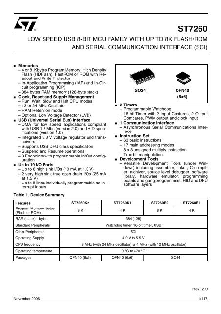
SO24<br />
QFN40<br />
(6x6)<br />
2 Timers<br />
– Programmable Watchdog<br />
– 16-bit Timer with 2 Input Captures, 2 Output<br />
Compares, PWM output and clock input<br />
1 Communication Interface<br />
– Asynchronous Serial Communications Interface<br />
Instruction Set<br />
– 63 basic instructions<br />
– 17 main addressing modes<br />
– 8 x 8 unsigned multiply instruction<br />
– True bit manipulation<br />
Development Tools<br />
– Versatile Development Tools (under Windows)<br />
including assembler, linker, C-compiler,<br />
archiver, source level debugger, software<br />
library, hardware emulator, programming<br />
boards and gang programmers, HID and DFU<br />
software layers<br />
Features <strong>ST7260</strong>K2 <strong>ST7260</strong>K1 <strong>ST7260</strong>E2 <strong>ST7260</strong>E1<br />
Program Memory -bytes<br />
(Flash or ROM)<br />
8 K 4 K 8 K 4 K<br />
RAM (stack) - bytes 384 (128)<br />
Standard Peripherals<br />
Watchdog timer, 16-bit timer, <strong>USB</strong><br />
Other Peripherals<br />
SCI<br />
Operating Supply<br />
4.0 V to 5.5 V<br />
CPU frequency 8 MHz (with 24 MHz oscillator) or 4 MHz (with 12 MHz oscillator)<br />
Operating temperature 0 °C to +70 °C<br />
Packages QFN40 (6x6) QFN40 (6x6) SO24<br />
Rev. 2.0<br />
November 2006 1/117<br />
1
Table of Contents<br />
1 INTRODUCTION . . . . . . . . . . . . . . . . . . . . . . . . . . . . . . . . . . . . . . . . . . . . . . . . . . . . . . . . . . . . . . 4<br />
2 PIN DESCRIPTION . . . . . . . . . . . . . . . . . . . . . . . . . . . . . . . . . . . . . . . . . . . . . . . . . . . . . . . . . . . . 5<br />
3 REGISTER & MEMORY MAP . . . . . . . . . . . . . . . . . . . . . . . . . . . . . . . . . . . . . . . . . . . . . . . . . . . 11<br />
4 FLASH PROGRAM MEMORY . . . . . . . . . . . . . . . . . . . . . . . . . . . . . . . . . . . . . . . . . . . . . . . . . . 14<br />
4.1 INTRODUCTION . . . . . . . . . . . . . . . . . . . . . . . . . . . . . . . . . . . . . . . . . . . . . . . . . . . . . . . . 14<br />
4.2 MAIN FEATURES . . . . . . . . . . . . . . . . . . . . . . . . . . . . . . . . . . . . . . . . . . . . . . . . . . . . . . . 14<br />
4.3 STRUCTURE . . . . . . . . . . . . . . . . . . . . . . . . . . . . . . . . . . . . . . . . . . . . . . . . . . . . . . . . . . . 14<br />
4.4 ICC INTERFACE . . . . . . . . . . . . . . . . . . . . . . . . . . . . . . . . . . . . . . . . . . . . . . . . . . . . . . . . 15<br />
4.5 ICP (IN-CIRCUIT PROGRAMMING) . . . . . . . . . . . . . . . . . . . . . . . . . . . . . . . . . . . . . . . . . 16<br />
4.6 IAP (IN-APPLICATION PROGRAMMING) . . . . . . . . . . . . . . . . . . . . . . . . . . . . . . . . . . . . . 16<br />
4.7 RELATED DOCUMENTATION . . . . . . . . . . . . . . . . . . . . . . . . . . . . . . . . . . . . . . . . . . . . . 16<br />
4.8 REGISTER DESCRIPTION . . . . . . . . . . . . . . . . . . . . . . . . . . . . . . . . . . . . . . . . . . . . . . . . 16<br />
5 CENTRAL PROCESSING UNIT . . . . . . . . . . . . . . . . . . . . . . . . . . . . . . . . . . . . . . . . . . . . . . . . . 17<br />
5.1 INTRODUCTION . . . . . . . . . . . . . . . . . . . . . . . . . . . . . . . . . . . . . . . . . . . . . . . . . . . . . . . . 17<br />
5.2 MAIN FEATURES . . . . . . . . . . . . . . . . . . . . . . . . . . . . . . . . . . . . . . . . . . . . . . . . . . . . . . . 17<br />
5.3 CPU REGISTERS . . . . . . . . . . . . . . . . . . . . . . . . . . . . . . . . . . . . . . . . . . . . . . . . . . . . . . . 17<br />
6 RESET AND CLOCK MANAGEMENT . . . . . . . . . . . . . . . . . . . . . . . . . . . . . . . . . . . . . . . . . . . . 20<br />
6.1 RESET . . . . . . . . . . . . . . . . . . . . . . . . . . . . . . . . . . . . . . . . . . . . . . . . . . . . . . . . . . . . . . . . 20<br />
6.2 CLOCK SYSTEM . . . . . . . . . . . . . . . . . . . . . . . . . . . . . . . . . . . . . . . . . . . . . . . . . . . . . . . . 22<br />
7 INTERR<strong>UP</strong>TS . . . . . . . . . . . . . . . . . . . . . . . . . . . . . . . . . . . . . . . . . . . . . . . . . . . . . . . . . . . . . . . 23<br />
7.1 INTERR<strong>UP</strong>T REGISTER . . . . . . . . . . . . . . . . . . . . . . . . . . . . . . . . . . . . . . . . . . . . . . . . . . 25<br />
8 POWER SAVING MODES . . . . . . . . . . . . . . . . . . . . . . . . . . . . . . . . . . . . . . . . . . . . . . . . . . . . . 26<br />
8.1 INTRODUCTION . . . . . . . . . . . . . . . . . . . . . . . . . . . . . . . . . . . . . . . . . . . . . . . . . . . . . . . . 26<br />
8.2 HALT MODE . . . . . . . . . . . . . . . . . . . . . . . . . . . . . . . . . . . . . . . . . . . . . . . . . . . . . . . . . . . 26<br />
8.3 S<strong>LOW</strong> MODE . . . . . . . . . . . . . . . . . . . . . . . . . . . . . . . . . . . . . . . . . . . . . . . . . . . . . . . . . . . 27<br />
8.4 WAIT MODE . . . . . . . . . . . . . . . . . . . . . . . . . . . . . . . . . . . . . . . . . . . . . . . . . . . . . . . . . . . 27<br />
9 I/O PORTS . . . . . . . . . . . . . . . . . . . . . . . . . . . . . . . . . . . . . . . . . . . . . . . . . . . . . . . . . . . . . . . . . . 28<br />
9.1 INTRODUCTION . . . . . . . . . . . . . . . . . . . . . . . . . . . . . . . . . . . . . . . . . . . . . . . . . . . . . . . . 28<br />
9.2 FUNCTIONAL DESCRIPTION . . . . . . . . . . . . . . . . . . . . . . . . . . . . . . . . . . . . . . . . . . . . . . 28<br />
10 MISCELLANEOUS REGISTER . . . . . . . . . . . . . . . . . . . . . . . . . . . . . . . . . . . . . . . . . . . . . . . . 35<br />
11 ON-CHIP PERIPHERALS . . . . . . . . . . . . . . . . . . . . . . . . . . . . . . . . . . . . . . . . . . . . . . . . . . . . . 36<br />
11.1 WATCHDOG TIMER (WDG) . . . . . . . . . . . . . . . . . . . . . . . . . . . . . . . . . . . . . . . . . . . . . . . 36<br />
11.2 16-<strong>BIT</strong> TIMER . . . . . . . . . . . . . . . . . . . . . . . . . . . . . . . . . . . . . . . . . . . . . . . . . . . . . . . . . . 39<br />
11.3 SERIAL COMMUNICATIONS INTERFACE (SCI) . . . . . . . . . . . . . . . . . . . . . . . . . . . . . . . 58<br />
11.4 <strong>USB</strong> INTERFACE (<strong>USB</strong>) . . . . . . . . . . . . . . . . . . . . . . . . . . . . . . . . . . . . . . . . . . . . . . . . . . 72<br />
12 INSTRUCTION SET . . . . . . . . . . . . . . . . . . . . . . . . . . . . . . . . . . . . . . . . . . . . . . . . . . . . . . . . . 80<br />
12.1 ST7 ADDRESSING MODES . . . . . . . . . . . . . . . . . . . . . . . . . . . . . . . . . . . . . . . . . . . . . . . 80<br />
12.2 INSTRUCTION GRO<strong>UP</strong>S . . . . . . . . . . . . . . . . . . . . . . . . . . . . . . . . . . . . . . . . . . . . . . . . . 83<br />
13 ELECTRICAL CHARACTERISTICS . . . . . . . . . . . . . . . . . . . . . . . . . . . . . . . . . . . . . . . . . . . . . 86<br />
13.1 PARAMETER CONDITIONS . . . . . . . . . . . . . . . . . . . . . . . . . . . . . . . . . . . . . . . . . . . . . . . 86<br />
13.2 ABSOLUTE MAXIMUM RATINGS . . . . . . . . . . . . . . . . . . . . . . . . . . . . . . . . . . . . . . .<br />
117<br />
. . . . 87<br />
13.3 OPERATING CONDITIONS . . . . . . . . . . . . . . . . . . . . . . . . . . . . . . . . . . . . . . . . . . . . . . . . 88<br />
2/117
Table of Contents<br />
13.4 S<strong>UP</strong>PLY CURRENT CHARACTERISTICS . . . . . . . . . . . . . . . . . . . . . . . . . . . . . . . . . . . . 89<br />
13.5 CLOCK AND TIMING CHARACTERISTICS . . . . . . . . . . . . . . . . . . . . . . . . . . . . . . . . . . . 90<br />
13.6 MEMORY CHARACTERISTICS . . . . . . . . . . . . . . . . . . . . . . . . . . . . . . . . . . . . . . . . . . . . 92<br />
13.7 EMC CHARACTERISTICS . . . . . . . . . . . . . . . . . . . . . . . . . . . . . . . . . . . . . . . . . . . . . . . . 93<br />
13.8 I/O PORT PIN CHARACTERISTICS . . . . . . . . . . . . . . . . . . . . . . . . . . . . . . . . . . . . . . . . . 95<br />
13.9 CONTROL PIN CHARACTERISTICS . . . . . . . . . . . . . . . . . . . . . . . . . . . . . . . . . . . . . . . . 99<br />
13.10COMMUNICATION INTERFACE CHARACTERISTICS . . . . . . . . . . . . . . . . . . . . . . . . 101<br />
14 PACKAGE CHARACTERISTICS . . . . . . . . . . . . . . . . . . . . . . . . . . . . . . . . . . . . . . . . . . . . . . 103<br />
14.1 PACKAGE MECHANICAL DATA . . . . . . . . . . . . . . . . . . . . . . . . . . . . . . . . . . . . . . . . . . . 103<br />
14.2 THERMAL CHARACTERISTICS . . . . . . . . . . . . . . . . . . . . . . . . . . . . . . . . . . . . . . . . . . 105<br />
14.3 SOLDERING AND GLUEABILITY INFORMATION . . . . . . . . . . . . . . . . . . . . . . . . . . . . . 106<br />
15 DEVICE CONFIGURATION AND ORDERING INFORMATION . . . . . . . . . . . . . . . . . . . . . . . 107<br />
15.1 OPTION BYTE . . . . . . . . . . . . . . . . . . . . . . . . . . . . . . . . . . . . . . . . . . . . . . . . . . . . . . . . . 107<br />
15.2 DEVICE ORDERING INFORMATION AND TRANSFER OF CUS<strong>TO</strong>MER CODE . . . . . 108<br />
15.3 DEVELOPMENT <strong>TO</strong>OLS . . . . . . . . . . . . . . . . . . . . . . . . . . . . . . . . . . . . . . . . . . . . . . . . . 109<br />
15.4 ST7 APPLICATION NOTES . . . . . . . . . . . . . . . . . . . . . . . . . . . . . . . . . . . . . . . . . . . . . . 111<br />
16 KNOWN LIMITATIONS . . . . . . . . . . . . . . . . . . . . . . . . . . . . . . . . . . . . . . . . . . . . . . . . . . . . . . 114<br />
16.1 PA2 LIMITATION <strong>WITH</strong> OCMP1 ENABLED . . . . . . . . . . . . . . . . . . . . . . . . . . . . . . . . . . 114<br />
16.2 UNEXPECTED RESET FETCH . . . . . . . . . . . . . . . . . . . . . . . . . . . . . . . . . . . . . . . . . . . . 114<br />
16.3 SCI WRONG BREAK DURATION . . . . . . . . . . . . . . . . . . . . . . . . . . . . . . . . . . . . . . . . . . 114<br />
16.4 <strong>USB</strong> BEHAVIOR <strong>WITH</strong> LVD DISABLED . . . . . . . . . . . . . . . . . . . . . . . . . . . . . . . . . . . . . 114<br />
17 REVISION HIS<strong>TO</strong>RY . . . . . . . . . . . . . . . . . . . . . . . . . . . . . . . . . . . . . . . . . . . . . . . . . . . . . . . . 116<br />
3/117
<strong>ST7260</strong><br />
1 INTRODUCTION<br />
The <strong>ST7260</strong> Microcontrollers form a sub-family of<br />
the ST7 <strong>MCU</strong>s dedicated to <strong>USB</strong> applications. The<br />
devices are based on an industry-standard 8-bit<br />
core and feature an enhanced instruction set.<br />
They operate at a 24 MHz or 12 MHz oscillator frequency.<br />
Under software control, the <strong>ST7260</strong><br />
<strong>MCU</strong>s may be placed in either Wait or Halt modes,<br />
thus reducing power consumption. The enhanced<br />
instruction set and addressing modes afford real<br />
programming potential. In addition to standard 8-<br />
bit data management, the <strong>ST7260</strong> <strong>MCU</strong>s feature<br />
true bit manipulation, 8x8 unsigned multiplication<br />
and indirect addressing modes. The devices include<br />
an ST7 Core, up to <strong>8K</strong>bytes of program<br />
memory, up to 384 bytes of RAM, 19 I/O lines and<br />
the following on-chip peripherals:<br />
– <strong>USB</strong> low speed interface with 3 endpoints with<br />
programmable in/out configuration using the<br />
DMA architecture with embedded 3.3V voltage<br />
regulator and transceivers (no external components<br />
are needed).<br />
– Industry standard asynchronous SCI serial interface<br />
– Watchdog<br />
– 16-bit Timer featuring an External clock input, 2<br />
Input Captures, 2 Output Compares with Pulse<br />
Generator capabilities<br />
– Low voltage reset (LVD) ensuring proper poweron<br />
or power-off of the device<br />
The ST72F60 devices are Flash versions. They<br />
support programming in IAP mode (In-application<br />
programming) via the on-chip <strong>USB</strong> interface.<br />
Figure 1. General Block Diagram<br />
OSCIN<br />
OSCOUT<br />
V DD<br />
V SS<br />
OSCILLA<strong>TO</strong>R<br />
POWER<br />
S<strong>UP</strong>PLY<br />
INTERNAL<br />
CLOCK<br />
OSC/3<br />
OSC/4 or OSC/2<br />
for <strong>USB</strong> 1)<br />
PORT A<br />
16-<strong>BIT</strong> TIMER<br />
PA[7:0]<br />
(8 bits)<br />
RESET<br />
WATCHDOG<br />
CONTROL<br />
8-<strong>BIT</strong> CORE<br />
ALU<br />
LVD<br />
<strong>USB</strong> DMA<br />
ADDRESS AND DATA BUS<br />
PORT B<br />
PORT C<br />
PB[7:0]<br />
(8 bits)<br />
V PP /TEST<br />
V DDA<br />
V SSA<br />
PROGRAM<br />
MEMORY<br />
(<strong>8K</strong> Bytes)<br />
RAM<br />
(384 Bytes)<br />
SCI<br />
(UART)<br />
<strong>USB</strong> SIE<br />
PC[2:0]<br />
(3 bits)<br />
<strong>USB</strong>DP<br />
<strong>USB</strong>DM<br />
<strong>USB</strong>VCC<br />
1) 12 or 24 MHz OSCIN frequency required to generate 6 MHz <strong>USB</strong> clock.<br />
4/117
<strong>ST7260</strong><br />
2 PIN DESCRIPTION<br />
Figure 2. 40-Lead QFN Package Pinout<br />
1<br />
40<br />
39<br />
38<br />
37<br />
36<br />
PA1(25mA)/ICCDATA<br />
NC<br />
NC<br />
NC<br />
NC<br />
NC<br />
NC<br />
NC<br />
NC<br />
PA2(25mA)/ICCCLK<br />
PA0/MCO<br />
35<br />
34<br />
33<br />
32<br />
31<br />
30<br />
PA3/EXTCLK<br />
V SSA<br />
2<br />
29<br />
PA4/ICAP1/IT1<br />
<strong>USB</strong>DP<br />
3<br />
28<br />
PA5/ICAP2/IT2<br />
<strong>USB</strong>DM<br />
4<br />
27<br />
PA6/OCMP1/IT3<br />
<strong>USB</strong>V CC<br />
5<br />
26<br />
PA7/OCMP2/IT4<br />
V DDA<br />
6<br />
25<br />
PB0(10mA)<br />
V DD<br />
7<br />
24<br />
PB1(10mA)<br />
OSCOUT<br />
8<br />
23<br />
PB2(10mA)<br />
OSCIN<br />
9<br />
22<br />
PB3(10mA)<br />
VSS<br />
10<br />
21<br />
PB4(10mA)/IT5<br />
11 12 13 14 15 16 17 18 19 20<br />
Note: NC=Do not connect<br />
<strong>USB</strong>OE/PC2<br />
TDO/PC1<br />
RDI/PC0<br />
RESET<br />
NC<br />
NC<br />
IT8/PB7(10mA)<br />
IT7/PB6(10mA)<br />
V PP /TEST<br />
IT6/PB5(10mA)<br />
5/117
<strong>ST7260</strong><br />
Figure 3. 24-Pin SO Package Pinout<br />
V DD<br />
OSCOUT<br />
OSCIN<br />
V SS<br />
TDO/PC1<br />
RDI/PC0<br />
RESET/<br />
IT7/PB6(10mA)<br />
V PP /TEST<br />
PB3(10mA)<br />
PB2(10mA)<br />
<strong>USB</strong>OE/PB1(10mA)<br />
1<br />
2<br />
3<br />
4<br />
5<br />
6<br />
7<br />
8<br />
9<br />
10<br />
11<br />
12<br />
24<br />
23<br />
22<br />
21<br />
20<br />
19<br />
18 PA2(25mA)/ICCCLK<br />
17<br />
16<br />
15<br />
14<br />
13<br />
<strong>USB</strong>Vcc<br />
<strong>USB</strong>DM<br />
<strong>USB</strong>DP<br />
V SSA<br />
PA0/MCO<br />
PA1(25mA)/ICCDATA<br />
PA3/EXTCLK<br />
PA4/ICAP1/IT1<br />
PA5/ICAP2/IT2<br />
PA7/OCMP2/IT4<br />
PB0(10mA)<br />
6/117
<strong>ST7260</strong><br />
PIN DESCRIPTION (Cont’d)<br />
RESET (see Note 1): Bidirectional. This active low<br />
signal forces the initialization of the <strong>MCU</strong>. This<br />
event is the top priority non maskable interrupt.<br />
This pin is switched low when the Watchdog is triggered<br />
or the V DD is low. It can be used to reset external<br />
peripherals.<br />
OSCIN/OSCOUT: Input/Output Oscillator pin.<br />
These pins connect a parallel-resonant crystal, or<br />
an external source, to the on-chip oscillator.<br />
V DD /V SS (see Note 2): Main Power Supply and<br />
Ground voltages.<br />
V DDA /V SSA (see Note 2): Power Supply and<br />
Ground voltages for analog peripherals.<br />
Alternate Functions: Several pins of the I/O ports<br />
assume software programmable alternate functions<br />
as shown in the pin description.<br />
Legend / Abbreviations for Table 2, Table 3:<br />
Type: I = input, O = output, S = supply<br />
In/Output level: C T = CMOS 0.3 V DD / 0.7 V DD with input trigger<br />
Output level: 10 mA = 10 mA high sink (Fn N-buffer only)<br />
25 mA = 25 mA very high sink (on N-buffer only)<br />
Port and control configuration:<br />
– Input: float = floating, wpu = weak pull-up, int = interrupt<br />
– Output: OD = open drain, PP = push-pull, T = True open drain<br />
The RESET configuration of each pin is shown in<br />
bold. This configuration is kept as long as the device<br />
is under reset state.<br />
Note 1: Adding two 100 nF decoupling capacitors<br />
on the Reset pin (respectively connected to V DD<br />
and V SS ) will significantly improve product electromagnetic<br />
susceptibility performance.<br />
Note 2: To enhance the reliability of operation, it is<br />
recommended that V DDA and V DD be connected together<br />
on the application board. This also applies<br />
to V SSA and V SS .<br />
Note 3: The <strong>USB</strong>OE alternate function is mapped<br />
on Port C2 in QFN40 devices. In SO24 devices it<br />
is mapped on Port B1.<br />
Note 4: The timer OCMP1 alternate function is<br />
mapped on Port A6 in QFN40 pin devices. In<br />
SO24 devices it is not available.<br />
7/117
<strong>ST7260</strong><br />
Table 2. Device Pin Description (QFN40)<br />
Pin n°<br />
QFN40<br />
Pin Name<br />
Type<br />
Input<br />
Level<br />
Output<br />
Port / Control<br />
Input Output<br />
Main<br />
Function<br />
(after reset)<br />
float<br />
wpu<br />
int<br />
OD<br />
PP<br />
Alternate Function<br />
7 V DD S Power supply voltage (4V - 5.5V)<br />
8 OSCOUT O Oscillator output<br />
9 OSCIN I Oscillator input<br />
10 V SS S Digital ground<br />
11 PC2/<strong>USB</strong>OE I/O C T X X Port C2 <strong>USB</strong> Output Enable<br />
12 PC1/TDO I/O C T X X Port C1 SCI Transmit Data Output<br />
13 PC0/RDI I/O C T X X Port C0 SCI Receive Data Input<br />
14 RESET I/O X X Reset<br />
15 NC -- Not connected<br />
16 NC -- Not connected<br />
17 PB7/IT8 I/O C T 10mA X X X Port B7<br />
18 PB6/IT7 I/O C T 10mA X X X Port B6<br />
19 V PP /TEST S Programming supply<br />
20 PB5/IT6 I/O C T 10mA X X X Port B5<br />
21 PB4/IT5 I/O C T 10mA X X X Port B4<br />
22 PB3 I/O C T 10mA X X Port B3<br />
23 PB2 I/O C T 10mA X X Port B2<br />
24 PB1 I/O C T 10mA X X Port B1<br />
25 PB0 I/O C T 10mA X X Port B0<br />
26 PA7/OCMP2/IT4 I/O C T X X X Port A7 Timer Output Compare 2<br />
27 PA6/OCMP1/IT3 I/O C T X X X Port A6 Timer Output Compare 1<br />
28 PA5/ICAP2/IT2 I/O C T X X X Port A5 Timer Input Capture 2<br />
29 PA4/ICAP1/IT1 I/O C T X X X Port A4 Timer Input Capture 1<br />
30 PA3/EXTCLK I/O C T X X Port A3 Timer External Clock<br />
31 PA2/ICCCLK I/O C T 25mA X T Port A2 ICC Clock<br />
32 NC -- Do not connect<br />
33 NC -- Do not connect<br />
34 NC -- Do not connect<br />
35 NC -- Do not connect<br />
36 NC -- Do not connect<br />
37 NC -- Do not connect<br />
38 NC -- Do not connect<br />
8/117
<strong>ST7260</strong><br />
Pin n°<br />
QFN40<br />
Pin Name<br />
Type<br />
Input<br />
Level<br />
Port / Control<br />
Input Output<br />
Main<br />
Function<br />
(after reset)<br />
39 NC -- Do not connect<br />
40 PA1/ICCDATA I/O C T 25mA X T Port A1 ICC Data<br />
1 PA0/MCO I/O C T X X Port A0 Main Clock Output<br />
2 V SSA S Analog ground<br />
Output<br />
float<br />
wpu<br />
3 <strong>USB</strong>DP I/O <strong>USB</strong> bidirectional data (data +)<br />
4 <strong>USB</strong>DM I/O <strong>USB</strong> bidirectional data (data -)<br />
5 <strong>USB</strong>VCC O <strong>USB</strong> power supply<br />
6 V DDA S Analog supply voltage<br />
int<br />
OD<br />
PP<br />
Alternate Function<br />
Table 3. Device Pin Description (SO24)<br />
Pin n°<br />
SO24<br />
Pin Name<br />
Type<br />
Input<br />
Level<br />
Output<br />
float<br />
Port / Control<br />
Input Output<br />
Main<br />
Function<br />
(after reset)<br />
Alternate Function<br />
1 V DD S Power supply voltage (4V - 5.5V)<br />
2 OSCOUT O Oscillator output<br />
3 OSCIN I Oscillator input<br />
4 V SS S Digital ground<br />
wpu<br />
5 PC1/TDO I/O C T X X Port C1 SCI Transmit Data Output<br />
6 PC0/RDI I/O C T X X Port C0 SCI Receive Data Input<br />
7 RESET I/O X X Reset<br />
8 PB6/IT7 I/O C T 10mA X X X Port B6<br />
9 V PP /TEST S Programming supply<br />
10 PB3 I/O C T 10mA X X Port B3<br />
11 PB2 I/O C T 10mA X X Port B2<br />
12 PB1/<strong>USB</strong>OE I/O C T 10mA X X Port B1 <strong>USB</strong> Output Enable<br />
13 PB0 I/O C T 10mA X X Port B0<br />
14 PA7/OCMP2/IT4 I/O C T X X X Port A7 Timer Output Compare 2<br />
15 PA5/ICAP2/IT2 I/O C T X X X Port A5 Timer Input Capture 2<br />
16 PA4/ICAP1/IT1 I/O C T X X X Port A4 Timer Input Capture 1<br />
17 PA3/EXTCLK I/O C T X X Port A3 Timer External Clock<br />
18 PA2/ICCCLK I/O C T 25mA X T Port A2 ICC Clock<br />
19 PA1/ICCDATA I/O C T 25mA X T Port A1 ICC Data<br />
int<br />
OD<br />
PP<br />
9/117
<strong>ST7260</strong><br />
Pin n°<br />
SO24<br />
Pin Name<br />
Type<br />
Input<br />
Level<br />
Port / Control<br />
Input Output<br />
Main<br />
Function<br />
(after reset)<br />
20 PA0/MCO I/O C T X X Port A0 Main Clock Output<br />
21 V SSA S Analog ground<br />
Output<br />
22 <strong>USB</strong>DP I/O <strong>USB</strong> bidirectional data (data +)<br />
23 <strong>USB</strong>DM I/O <strong>USB</strong> bidirectional data (data -)<br />
24 <strong>USB</strong>VCC O <strong>USB</strong> power supply<br />
float<br />
wpu<br />
int<br />
OD<br />
PP<br />
Alternate Function<br />
10/117
<strong>ST7260</strong><br />
3 REGISTER & MEMORY MAP<br />
As shown in Figure 4, the <strong>MCU</strong> is capable of addressing<br />
8 Kbytes of memories and I/O registers.<br />
The available memory locations consist of up to<br />
384 bytes of RAM including 64 bytes of register locations,<br />
and up to <strong>8K</strong> bytes of user program memory<br />
in which the upper 32 bytes are reserved for interrupt<br />
vectors. The RAM space includes up to 128<br />
bytes for the stack from 0100h to 017Fh.<br />
The highest address bytes contain the user reset<br />
and interrupt vectors.<br />
IMPORTANT: Memory locations noted “Reserved”<br />
must never be accessed. Accessing a reserved<br />
area can have unpredictable effects on the<br />
device.<br />
Figure 4. Memory Map<br />
0000h<br />
003Fh<br />
0040h<br />
01BFh<br />
01C0h<br />
7FFFh<br />
8000h<br />
FFDFh<br />
FFE0h<br />
FFFFh<br />
HW Registers<br />
(See Table 5)<br />
RAM<br />
(384 Bytes)<br />
Reserved<br />
Program Memory<br />
(4 / 8 KBytes)<br />
Interrupt & Reset Vectors<br />
(See Table 4)<br />
E000h<br />
F000h<br />
FFDFh<br />
0040h<br />
00FFh<br />
0100h<br />
017Fh<br />
0180h<br />
01BFh<br />
8 KBytes<br />
4 KBytes<br />
Short Addressing<br />
RAM (192 bytes)<br />
Stack<br />
(128 Bytes)<br />
16-bit Addressing<br />
RAM<br />
Table 4. Interrupt Vector Map<br />
Vector Address Description Masked by Remarks Exit from Halt Mode<br />
FFE0h-FFEDh<br />
FFEEh-FFEFh<br />
FFF0h-FFF1h<br />
FFF2h-FFF3h<br />
FFF4h-FFF5h<br />
FFF6h-FFF7h<br />
FFF8h-FFF9h<br />
FFFAh-FFFBh<br />
FFFCh-FFFDh<br />
FFFEh-FFFFh<br />
Reserved Area<br />
<strong>USB</strong> Interrupt Vector<br />
SCI Interrupt Vector<br />
Reserved Area<br />
TIMER Interrupt Vector<br />
IT1 to IT8 Interrupt Vector<br />
<strong>USB</strong> End Suspend Mode Interrupt Vector<br />
Flash Start Programming Interrupt Vector<br />
TRAP (software) Interrupt Vector<br />
RESET Vector<br />
I- bit<br />
I- bit<br />
I- bit<br />
I- bit<br />
I- bit<br />
I- bit<br />
None<br />
None<br />
Internal Interrupt<br />
Internal Interrupt<br />
Internal Interrupt<br />
External Interrupt<br />
External Interrupts<br />
Internal Interrupt<br />
CPU Interrupt<br />
No<br />
No<br />
No<br />
Yes<br />
Yes<br />
Yes<br />
No<br />
Yes<br />
11/117
<strong>ST7260</strong><br />
Table 5. Hardware Register Memory Map<br />
Address Block Register Label Register name Reset Status Remarks<br />
0000h<br />
PADR<br />
Port A Data Register<br />
00h<br />
R/W<br />
Port A<br />
0001h<br />
PADDR Port A Data Direction Register<br />
00h<br />
R/W<br />
0002h<br />
PBDR<br />
Port B Data Register<br />
00h<br />
R/W<br />
Port B<br />
0003h<br />
PBDDR Port B Data Direction Register<br />
00h<br />
R/W<br />
0004h<br />
PCDR<br />
Port C Data Register<br />
1111 x000b R/W<br />
Port C<br />
0005h<br />
PCDDR Port C Data Direction Register<br />
1111 x000b R/W<br />
0006h<br />
to<br />
Reserved (2 bytes)<br />
0007h<br />
0008h ITC ITIFRE Interrupt Register 00h R/W<br />
0009h MISC MISCR Miscellaneous Register 00h R/W<br />
000Ah<br />
to<br />
Reserved (2 bytes)<br />
000Bh<br />
000Ch WDG WDGCR Watchdog Control Register 7Fh R/W<br />
000Dh<br />
to<br />
0010h<br />
Reserved (4 bytes)<br />
0011h<br />
0012h<br />
0013h<br />
0014h<br />
0015h<br />
0016h<br />
0017h<br />
0018h<br />
0019h<br />
001Ah<br />
001Bh<br />
001Ch<br />
001Dh<br />
001Eh<br />
001Fh<br />
0020h<br />
0021h<br />
0022h<br />
0023h<br />
0024h<br />
TIM<br />
SCI<br />
TCR2<br />
TCR1<br />
TCSR<br />
TIC1HR<br />
TIC1LR<br />
<strong>TO</strong>C1HR<br />
<strong>TO</strong>C1LR<br />
TCHR<br />
TCLR<br />
TACHR<br />
TACLR<br />
TIC2HR<br />
TIC2LR<br />
<strong>TO</strong>C2HR<br />
<strong>TO</strong>C2LR<br />
SCISR<br />
SCIDR<br />
SCIBRR<br />
SCICR1<br />
SCICR2<br />
Timer Control Register 2<br />
Timer Control Register 1<br />
Timer Control/Status Register<br />
Timer Input Capture High Register 1<br />
Timer Input Capture Low Register 1<br />
Timer Output Compare High Register 1<br />
Timer Output Compare Low Register 1<br />
Timer Counter High Register<br />
Timer Counter Low Register<br />
Timer Alternate Counter High Register<br />
Timer Alternate Counter Low Register<br />
Timer Input Capture High Register 2<br />
Timer Input Capture Low Register 2<br />
Timer Output Compare High Register 2<br />
Timer Output Compare Low Register 2<br />
SCI Status Register<br />
SCI Data Register<br />
SCI Baud Rate Register<br />
SCI Control Register 1<br />
SCI Control Register 2<br />
00h<br />
00h<br />
00h<br />
xxh<br />
xxh<br />
80h<br />
00h<br />
FFh<br />
FCh<br />
FFh<br />
FCh<br />
xxh<br />
xxh<br />
80h<br />
00h<br />
C0h<br />
xxh<br />
00h<br />
x000 0000b<br />
00h<br />
R/W<br />
R/W<br />
R/W<br />
Read only<br />
Read only<br />
R/W<br />
R/W<br />
Read only<br />
R/W<br />
Read only<br />
R/W<br />
Read only<br />
Read only<br />
R/W<br />
R/W<br />
Read only<br />
R/W<br />
R/W<br />
R/W<br />
R/W<br />
12/117
<strong>ST7260</strong><br />
Address Block Register Label Register name Reset Status Remarks<br />
0025h<br />
0026h<br />
0027h<br />
0028h<br />
0029h<br />
002Ah<br />
002Bh<br />
002Ch<br />
002Dh<br />
002Eh<br />
002Fh<br />
0030h<br />
0031h<br />
<strong>USB</strong><br />
<strong>USB</strong>PIDR<br />
<strong>USB</strong>DMAR<br />
<strong>USB</strong>IDR<br />
<strong>USB</strong>ISTR<br />
<strong>USB</strong>IMR<br />
<strong>USB</strong>CTLR<br />
<strong>USB</strong>DADDR<br />
<strong>USB</strong>EP0RA<br />
<strong>USB</strong>EP0RB<br />
<strong>USB</strong>EP1RA<br />
<strong>USB</strong>EP1RB<br />
<strong>USB</strong>EP2RA<br />
<strong>USB</strong>EP2RB<br />
<strong>USB</strong> PID Register<br />
<strong>USB</strong> DMA address Register<br />
<strong>USB</strong> Interrupt/DMA Register<br />
<strong>USB</strong> Interrupt Status Register<br />
<strong>USB</strong> Interrupt Mask Register<br />
<strong>USB</strong> Control Register<br />
<strong>USB</strong> Device Address Register<br />
<strong>USB</strong> Endpoint 0 Register A<br />
<strong>USB</strong> Endpoint 0 Register B<br />
<strong>USB</strong> Endpoint 1 Register A<br />
<strong>USB</strong> Endpoint 1 Register B<br />
<strong>USB</strong> Endpoint 2 Register A<br />
<strong>USB</strong> Endpoint 2 Register B<br />
x0h<br />
xxh<br />
x0h<br />
00h<br />
00h<br />
06h<br />
00h<br />
0000 xxxxb<br />
80h<br />
0000 xxxxb<br />
0000 xxxxb<br />
0000 xxxxb<br />
0000 xxxxb<br />
Read only<br />
R/W<br />
R/W<br />
R/W<br />
R/W<br />
R/W<br />
R/W<br />
R/W<br />
R/W<br />
R/W<br />
R/W<br />
R/W<br />
R/W<br />
0032h<br />
0036h<br />
Reserved (5 Bytes)<br />
0037h Flash FCSR Flash Control /Status Register 00h R/W<br />
0038h<br />
to<br />
003Fh<br />
Reserved (8 bytes)<br />
13/117
<strong>ST7260</strong><br />
4 FLASH PROGRAM MEMORY<br />
4.1 INTRODUCTION<br />
The ST7 dual voltage High Density Flash<br />
(HDFlash) is a non-volatile memory that can be<br />
electrically erased as a single block or by individual<br />
sectors and programmed on a Byte-by-Byte basis<br />
using an external V PP supply.<br />
The HDFlash devices can be programmed and<br />
erased off-board (plugged in a programming tool)<br />
or on-board using ICP (In-Circuit Programming) or<br />
IAP (In-Application Programming).<br />
The array matrix organisation allows each sector<br />
to be erased and reprogrammed without affecting<br />
other sectors.<br />
4.2 MAIN FEATURES<br />
■ 3 Flash programming modes:<br />
– Insertion in a programming tool. In this mode,<br />
all sectors including option bytes can be programmed<br />
or erased.<br />
– ICP (In-Circuit Programming). In this mode, all<br />
sectors including option bytes can be programmed<br />
or erased without removing the device<br />
from the application board.<br />
– IAP (In-Application Programming) In this<br />
mode, all sectors except Sector 0, can be programmed<br />
or erased without removing the device<br />
from the application board and while the<br />
application is running.<br />
■ ICT (In-Circuit Testing) for downloading and<br />
executing user application test patterns in RAM<br />
■ Read-out protection<br />
■ Register Access Security System (RASS) to<br />
prevent accidental programming or erasing<br />
4.3 STRUCTURE<br />
The Flash memory is organised in sectors and can<br />
be used for both code and data storage.<br />
Depending on the overall Flash memory size in the<br />
microcontroller device, there are up to three user<br />
sectors (see Table 6). Each of these sectors can<br />
be erased independently to avoid unnecessary<br />
erasing of the whole Flash memory when only a<br />
partial erasing is required.<br />
The first two sectors have a fixed size of 4 Kbytes<br />
(see Figure 5). They are mapped in the upper part<br />
of the ST7 addressing space so the reset and interrupt<br />
vectors are located in Sector 0 (F000h-<br />
FFFFh).<br />
Table 6. Sectors available in Flash devices<br />
Flash Size (bytes) Available Sectors<br />
4K Sector 0<br />
<strong>8K</strong> Sectors 0,1<br />
> <strong>8K</strong> Sectors 0,1, 2<br />
4.3.1 Read-out Protection<br />
Read-out protection, when selected, provides a<br />
protection against Program Memory content extraction<br />
and against write access to Flash memory.<br />
Even if no protection can be considered as totally<br />
unbreakable, the feature provides a very high<br />
level of protection for a general purpose microcontroller.<br />
In Flash devices, this protection is removed by reprogramming<br />
the option. In this case, the entire<br />
program memory is first automatically erased and<br />
the device can be reprogrammed.<br />
Read-out protection selection depends on the device<br />
type:<br />
– In Flash devices it is enabled and removed<br />
through the FMP_R bit in the option byte.<br />
– In ROM devices it is enabled by mask option<br />
specified in the Option List.<br />
Figure 5. Memory Map and Sector Address<br />
1000h<br />
3FFFh<br />
7FFFh<br />
9FFFh<br />
BFFFh<br />
D7FFh<br />
DFFFh<br />
EFFFh<br />
FFFFh<br />
4K <strong>8K</strong> 10K 16K 24K 32K 4<strong>8K</strong> 60K FLASH<br />
MEMORY SIZE<br />
SEC<strong>TO</strong>R 2<br />
2Kbytes 8 Kbytes 16 Kbytes<br />
4 Kbytes<br />
4 Kbytes<br />
24 Kbytes 40 Kbytes 52 Kbytes<br />
SEC<strong>TO</strong>R 1<br />
SEC<strong>TO</strong>R 0<br />
14/117
<strong>ST7260</strong><br />
FLASH PROGRAM MEMORY (Cont’d)<br />
4.4 ICC INTERFACE<br />
ICC (In-Circuit Communication) needs a minimum<br />
of four and up to six pins to be connected to the<br />
programming tool (see Figure 6). These pins are:<br />
– RESET: device reset<br />
–V SS : device power supply ground<br />
Figure 6. Typical ICC Interface<br />
PROGRAMMING <strong>TO</strong>OL<br />
– ICCCLK: ICC output serial clock pin<br />
– ICCDATA: ICC input/output serial data pin<br />
– ICCSEL/V PP : programming voltage<br />
– OSC1(or OSCIN): main clock input for external<br />
source (optional)<br />
–V DD : application board power supply (see Figure<br />
6, Note 3)<br />
ICC CONNEC<strong>TO</strong>R<br />
ICC Cable<br />
APPLICATION BOARD<br />
(See Note 3)<br />
OPTIONAL<br />
(See Note 4)<br />
9 7 5 3<br />
1<br />
ICC CONNEC<strong>TO</strong>R<br />
HE10 CONNEC<strong>TO</strong>R TYPE<br />
10<br />
8<br />
6<br />
4<br />
2<br />
APPLICATION<br />
RESET SOURCE<br />
See Note 2<br />
10kΩ<br />
APPLICATION<br />
POWER S<strong>UP</strong>PLY<br />
C L2<br />
C L1<br />
See Note 1<br />
V DD<br />
OSC2<br />
OSC1<br />
ST7<br />
V SS<br />
ICCSEL/VPP<br />
RESET<br />
ICCCLK<br />
ICCDATA<br />
APPLICATION<br />
I/O<br />
Notes:<br />
1. If the ICCCLK or ICCDATA pins are only used<br />
as outputs in the application, no signal isolation is<br />
necessary. As soon as the Programming Tool is<br />
plugged to the board, even if an ICC session is not<br />
in progress, the ICCCLK and ICCDATA pins are<br />
not available for the application. If they are used as<br />
inputs by the application, isolation such as a serial<br />
resistor has to implemented in case another device<br />
forces the signal. Refer to the Programming<br />
Tool documentation for recommended resistor values.<br />
2. During the ICC session, the programming tool<br />
must control the RESET pin. This can lead to conflicts<br />
between the programming tool and the application<br />
reset circuit if it drives more than 5mA at<br />
high level (push pull output or pull-up resistor 1K or a reset management<br />
IC with open drain output and pull-up<br />
resistor > 1K, no additional components are needed.<br />
In all cases the user must ensure that no external<br />
reset is generated by the application during the<br />
ICC session.<br />
3. The use of Pin 7 of the ICC connector depends<br />
on the Programming Tool architecture. This pin<br />
must be connected when using most ST Programming<br />
Tools (it is used to monitor the application<br />
power supply). Please refer to the Programming<br />
Tool manual.<br />
4. Pin 9 has to be connected to the OSC1 or OS-<br />
CIN pin of the ST7 when the clock is not available<br />
in the application or if the selected clock option is<br />
not programmed in the option byte. ST7 devices<br />
with multi-oscillator capability need to have OSC2<br />
grounded in this case.<br />
15/117
<strong>ST7260</strong><br />
FLASH PROGRAM MEMORY (Cont’d)<br />
4.5 ICP (IN-CIRCUIT PROGRAMMING)<br />
To perform ICP the microcontroller must be<br />
switched to ICC (In-Circuit Communication) mode<br />
by an external controller or programming tool.<br />
Depending on the ICP code downloaded in RAM,<br />
Flash memory programming can be fully customized<br />
(number of bytes to program, program locations,<br />
or selection serial communication interface<br />
for downloading).<br />
When using an STMicroelectronics or third-party<br />
programming tool that supports ICP and the specific<br />
microcontroller device, the user needs only to<br />
implement the ICP hardware interface on the application<br />
board (see Figure 6). For more details on<br />
the pin locations, refer to the device pinout description.<br />
4.6 IAP (IN-APPLICATION PROGRAMMING)<br />
This mode uses a BootLoader program previously<br />
stored in Sector 0 by the user (in ICP mode or by<br />
plugging the device in a programming tool).<br />
This mode is fully controlled by user software. This<br />
allows it to be adapted to the user application, (user-defined<br />
strategy for entering programming<br />
mode, choice of communications protocol used to<br />
fetch the data to be stored, etc.). For example, it is<br />
possible to download code from the SPI, SCI or<br />
other type of serial interface and program it in the<br />
Flash. IAP mode can be used to program any of<br />
the Flash sectors except Sector 0, which is write/<br />
erase protected to allow recovery in case errors<br />
occur during the programming operation.<br />
4.7 RELATED DOCUMENTATION<br />
For details on Flash programming and ICC protocol,<br />
refer to the ST7 Flash Programming Reference<br />
Manual and to the ST7 ICC Protocol Reference<br />
Manual.<br />
4.8 REGISTER DESCRIPTION<br />
FLASH CONTROL/STATUS REGISTER (FCSR)<br />
Read/Write<br />
Reset Value: 0000 0000 (00h)<br />
7 0<br />
0 0 0 0 0 0 0 0<br />
This register is reserved for use by Programming<br />
Tool software. It controls the Flash programming<br />
and erasing operations.<br />
16/117
<strong>ST7260</strong><br />
5 CENTRAL PROCESSING UNIT<br />
5.1 INTRODUCTION<br />
This CPU has a full 8-bit architecture and contains<br />
six internal registers allowing efficient 8-bit data<br />
manipulation.<br />
5.2 MAIN FEATURES<br />
■ 63 basic instructions<br />
■ Fast 8-bit by 8-bit multiply<br />
■ 17 main addressing modes<br />
■ Two 8-bit index registers<br />
■ 16-bit stack pointer<br />
■ Low power modes<br />
■ Maskable hardware interrupts<br />
■ Non-maskable software interrupt<br />
5.3 CPU REGISTERS<br />
The six CPU registers shown in Figure 7 are not<br />
present in the memory mapping and are accessed<br />
by specific instructions.<br />
Accumulator (A)<br />
The Accumulator is an 8-bit general purpose register<br />
used to hold operands and the results of the<br />
arithmetic and logic calculations and to manipulate<br />
data.<br />
Index Registers (X and Y)<br />
In indexed addressing modes, these 8-bit registers<br />
are used to create either effective addresses or<br />
temporary storage areas for data manipulation.<br />
(The Cross-Assembler generates a precede instruction<br />
(PRE) to indicate that the following instruction<br />
refers to the Y register.)<br />
The Y register is not affected by the interrupt automatic<br />
procedures (not pushed to and popped from<br />
the stack).<br />
Program Counter (PC)<br />
The program counter is a 16-bit register containing<br />
the address of the next instruction to be executed<br />
by the CPU. It is made of two 8-bit registers PCL<br />
(Program Counter Low which is the LSB) and PCH<br />
(Program Counter High which is the MSB).<br />
Figure 7. CPU Registers<br />
7 0<br />
15 PCH 8<br />
7 0<br />
7 0<br />
RESET VALUE = RESET VEC<strong>TO</strong>R @ FFFEh-FFFFh<br />
7<br />
RESET VALUE = 1<br />
RESET VALUE = XXh<br />
RESET VALUE = XXh<br />
RESET VALUE = XXh<br />
PCL<br />
7 0<br />
1 1 1 H I N Z C<br />
1 1 X 1 X X<br />
0<br />
X<br />
ACCUMULA<strong>TO</strong>R<br />
X INDEX REGISTER<br />
Y INDEX REGISTER<br />
PROGRAM COUNTER<br />
CONDITION CODE REGISTER<br />
15 8 7 0<br />
RESET VALUE = STACK HIGHER ADDRESS<br />
STACK POINTER<br />
X = Undefined Value<br />
17/117
<strong>ST7260</strong><br />
CPU REGISTERS (Cont’d)<br />
CONDITION CODE REGISTER (CC)<br />
Read/Write<br />
Reset Value: 111x1xxx<br />
7 0<br />
because the I bit is set by hardware at the start of<br />
the routine and reset by the IRET instruction at the<br />
end of the routine. If the I bit is cleared by software<br />
in the interrupt routine, pending interrupts are<br />
serviced regardless of the priority level of the current<br />
interrupt routine.<br />
1 1 1 H I N Z C<br />
The 8-bit Condition Code register contains the interrupt<br />
mask and four flags representative of the<br />
result of the instruction just executed. This register<br />
can also be handled by the PUSH and POP instructions.<br />
These bits can be individually tested and/or controlled<br />
by specific instructions.<br />
Bit 4 = H Half carry<br />
This bit is set by hardware when a carry occurs between<br />
bits 3 and 4 of the ALU during an ADD or<br />
ADC instruction. It is reset by hardware during the<br />
same instructions.<br />
0: No half carry has occurred.<br />
1: A half carry has occurred.<br />
This bit is tested using the JRH or JRNH instruction.<br />
The H bit is useful in BCD arithmetic subroutines.<br />
Bit 3 = I Interrupt mask<br />
This bit is set by hardware when entering in interrupt<br />
or by software to disable all interrupts except<br />
the TRAP software interrupt. This bit is cleared by<br />
software.<br />
0: Interrupts are enabled.<br />
1: Interrupts are disabled.<br />
This bit is controlled by the RIM, SIM and IRET instructions<br />
and is tested by the JRM and JRNM instructions.<br />
Note: Interrupts requested while I is set are<br />
latched and can be processed when I is cleared.<br />
By default an interrupt routine is not interruptible<br />
Bit 2 = N Negative<br />
This bit is set and cleared by hardware. It is representative<br />
of the result sign of the last arithmetic,<br />
logical or data manipulation. It is a copy of the 7 th<br />
bit of the result.<br />
0: The result of the last operation is positive or null.<br />
1: The result of the last operation is negative<br />
(that is, the most significant bit is a logic 1).<br />
This bit is accessed by the JRMI and JRPL instructions.<br />
Bit 1 = Z Zero<br />
This bit is set and cleared by hardware. This bit indicates<br />
that the result of the last arithmetic, logical<br />
or data manipulation is zero.<br />
0: The result of the last operation is different from<br />
zero.<br />
1: The result of the last operation is zero.<br />
This bit is accessed by the JREQ and JRNE test<br />
instructions.<br />
Bit 0 = C Carry/borrow<br />
This bit is set and cleared by hardware and software.<br />
It indicates an overflow or an underflow has<br />
occurred during the last arithmetic operation.<br />
0: No overflow or underflow has occurred.<br />
1: An overflow or underflow has occurred.<br />
This bit is driven by the SCF and RCF instructions<br />
and tested by the JRC and JRNC instructions. It is<br />
also affected by the “bit test and branch”, shift and<br />
rotate instructions.<br />
18/117
<strong>ST7260</strong><br />
CPU REGISTERS (Cont’d)<br />
STACK POINTER (SP)<br />
Read/Write<br />
Reset Value: 017Fh<br />
15 8<br />
0 0 0 0 0 0 0 1<br />
7 0<br />
0 SP6 SP5 SP4 SP3 SP2 SP1 SP0<br />
The Stack Pointer is a 16-bit register which is always<br />
pointing to the next free location in the stack.<br />
It is then decremented after data has been pushed<br />
onto the stack and incremented before data is<br />
popped from the stack (see Figure 8).<br />
Since the stack is 128 bytes deep, the 9 most significant<br />
bits are forced by hardware. Following an<br />
<strong>MCU</strong> Reset, or after a Reset Stack Pointer instruction<br />
(RSP), the Stack Pointer contains its reset value<br />
(the SP6 to SP0 bits are set) which is the stack<br />
higher address.<br />
The least significant byte of the Stack Pointer<br />
(called S) can be directly accessed by a LD instruction.<br />
Note: When the lower limit is exceeded, the Stack<br />
Pointer wraps around to the stack upper limit, without<br />
indicating the stack overflow. The previously<br />
stored information is then overwritten and therefore<br />
lost. The stack also wraps in case of an underflow.<br />
The stack is used to save the return address during<br />
a subroutine call and the CPU context during<br />
an interrupt. The user may also directly manipulate<br />
the stack by means of the PUSH and POP instructions.<br />
In the case of an interrupt, the PCL is stored<br />
at the first location pointed to by the SP. Then the<br />
other registers are stored in the next locations as<br />
shown in Figure 8.<br />
– When an interrupt is received, the SP is decremented<br />
and the context is pushed on the stack.<br />
– On return from interrupt, the SP is incremented<br />
and the context is popped from the stack.<br />
A subroutine call occupies two locations and an interrupt<br />
five locations in the stack area.<br />
Figure 8. Stack Manipulation Example<br />
@ 0100h<br />
CALL<br />
Subroutine<br />
Interrupt<br />
Event<br />
PUSH Y POP Y IRET RET<br />
or RSP<br />
SP<br />
SP<br />
@ 017Fh<br />
PCH<br />
PCL<br />
SP<br />
CC<br />
A<br />
X<br />
PCH<br />
PCL<br />
PCH<br />
PCL<br />
Y<br />
CC<br />
A<br />
X<br />
PCH<br />
PCL<br />
PCH<br />
PCL<br />
SP<br />
CC<br />
A<br />
X<br />
PCH<br />
PCL<br />
PCH<br />
PCL<br />
SP<br />
PCH<br />
PCL<br />
SP<br />
Stack Higher Address = 017Fh<br />
Stack Lower Address = 0100h<br />
19/117
<strong>ST7260</strong><br />
6 RESET AND CLOCK MANAGEMENT<br />
6.1 RESET<br />
The Reset procedure is used to provide an orderly<br />
software start-up or to exit low power modes.<br />
Three reset modes are provided: a low voltage<br />
(LVD) reset, a watchdog reset and an external reset<br />
at the RESET pin.<br />
A reset causes the reset vector to be fetched from<br />
addresses FFFEh and FFFFh in order to be loaded<br />
into the PC and with program execution starting<br />
from this point.<br />
An internal circuitry provides a 4096 CPU clock cycle<br />
delay from the time that the oscillator becomes<br />
active.<br />
6.1.1 Low Voltage Detector (LVD)<br />
Low voltage reset circuitry generates a reset when<br />
V DD is:<br />
■ below V IT+ when V DD is rising,<br />
■ below V IT- when V DD is falling.<br />
During low voltage reset, the RESET pin is held low,<br />
thus permitting the <strong>MCU</strong> to reset other devices.<br />
It is recommended to make sure that the V DD supply<br />
voltage rises monotonously when the device is<br />
exiting from Reset, to ensure the application functions<br />
properly.<br />
6.1.3 External Reset<br />
The external reset is an active low input signal applied<br />
to the RESET pin of the <strong>MCU</strong>.<br />
As shown in Figure 12, the RESET signal must<br />
stay low for a minimum of one and a half CPU<br />
clock cycles.<br />
An internal Schmitt trigger at the RESET pin is provided<br />
to improve noise immunity.<br />
Figure 9. Low Voltage Detector functional Diagram<br />
V DD<br />
<strong>LOW</strong> VOLTAGE<br />
DETEC<strong>TO</strong>R<br />
FROM<br />
WATCHDOG<br />
RESET<br />
RESET<br />
INTERNAL<br />
RESET<br />
Figure 10. Low Voltage Reset Signal Output<br />
V DD<br />
V IT+<br />
V IT-<br />
6.1.2 Watchdog Reset<br />
When a watchdog reset occurs, the RESET pin is<br />
pulled low permitting the <strong>MCU</strong> to reset other devices<br />
in the same way as the low voltage reset (Figure<br />
9).<br />
RESET<br />
Figure 11. Temporization timing diagram after an internal Reset<br />
Note: Hysteresis (V IT+ -V IT- ) = V hys<br />
V DD<br />
V IT+<br />
Temporization (4096 CPU clock cycles)<br />
Addresses<br />
$FFFE<br />
20/117
<strong>ST7260</strong><br />
RESET (Cont’d)<br />
Figure 12. Reset Timing Diagram<br />
t DDR<br />
V DD<br />
OSCIN<br />
t OXOV<br />
f CPU<br />
PC<br />
FFFE<br />
FFFF<br />
RESET<br />
WATCHDOG RESET<br />
4096 CPU<br />
CLOCK<br />
CYCLES<br />
DELAY<br />
Note: Refer to Electrical Characteristics for values of t DDR , t OXOV , V IT+ , V IT- and V hys<br />
21/117
<strong>ST7260</strong><br />
6.2 CLOCK SYSTEM<br />
6.2.1 General Description<br />
The <strong>MCU</strong> accepts either a Crystal or Ceramic resonator,<br />
or an external clock signal to drive the internal<br />
oscillator. The internal clock (f CPU ) is derived<br />
from the external oscillator frequency (f OSC ),<br />
which is divided by 3 (and by 2 or 4 for <strong>USB</strong>, depending<br />
on the external clock used). The internal<br />
clock is further divided by 2 by setting the SMS bit<br />
in the Miscellaneous Register.<br />
Using the OSC24/12 bit in the option byte, a 12<br />
MHz or a 24 MHz external clock can be used to<br />
provide an internal frequency of either 2, 4 or 8<br />
MHz while maintaining a 6 MHz for the <strong>USB</strong> (refer<br />
to Figure 15).<br />
The internal clock signal (f CPU ) is also routed to<br />
the on-chip peripherals. The CPU clock signal<br />
consists of a square wave with a duty cycle of<br />
50%.<br />
The internal oscillator is designed to operate with<br />
an AT-cut parallel resonant quartz or ceramic resonator<br />
in the frequency range specified for f osc .<br />
The circuit shown in Figure 14 is recommended<br />
when using a crystal, and Table 7, "Recommended<br />
Values for 24 MHz Crystal Resonator" lists the<br />
recommended capacitance. The crystal and associated<br />
components should be mounted as close as<br />
possible to the input pins in order to minimize output<br />
distortion and start-up stabilisation time.<br />
Table 7. Recommended Values for 24 MHz<br />
Crystal Resonator<br />
R SMAX 20 Ω 25 Ω 70 Ω<br />
C OSCIN 56pF 47pF 22pF<br />
C OSCOUT 56pF 47pF 22pF<br />
R P 1-10 MΩ 1-10 MΩ 1-10 MΩ<br />
Note: R SMAX is the equivalent serial resistor of the<br />
crystal (see crystal specification).<br />
6.2.2 External Clock<br />
An external clock may be applied to the OSCIN input<br />
with the OSCOUT pin not connected, as<br />
shown on Figure 13. The t OXOV specifications do<br />
not apply when using an external clock input. The<br />
equivalent specification of the external clock<br />
source should be used instead of t OXOV (see Section<br />
6.5 CONTROL TIMING).<br />
Figure 13. External Clock Source Connections<br />
OSCIN<br />
EXTERNAL<br />
CLOCK<br />
OSCOUT<br />
NC<br />
Figure 14. Crystal/Ceramic Resonator<br />
C OSCIN<br />
OSCIN<br />
R P<br />
OSCOUT<br />
Figure 15. Clock Block Diagram<br />
24 or<br />
12 MHz<br />
Crystal<br />
%3<br />
%2<br />
1<br />
0<br />
%2<br />
OSC24/12<br />
C OSCOUT<br />
0<br />
1<br />
%2<br />
SMS<br />
8, 4 or 2 MHz<br />
CPU and<br />
peripherals)<br />
6 MHz (<strong>USB</strong>)<br />
22/117
<strong>ST7260</strong><br />
7 INTERR<strong>UP</strong>TS<br />
The ST7 core may be interrupted by one of two different<br />
methods: maskable hardware interrupts as<br />
listed in Table 8, "Interrupt Mapping" and a nonmaskable<br />
software interrupt (TRAP). The Interrupt<br />
processing flowchart is shown in Figure 16.<br />
The maskable interrupts must be enabled clearing<br />
the I bit in order to be serviced. However, disabled<br />
interrupts may be latched and processed when<br />
they are enabled (see external interrupts subsection).<br />
When an interrupt has to be serviced:<br />
– Normal processing is suspended at the end of<br />
the current instruction execution.<br />
– The PC, X, A and CC registers are saved onto<br />
the stack.<br />
– The I bit of the CC register is set to prevent additional<br />
interrupts.<br />
– The PC is then loaded with the interrupt vector of<br />
the interrupt to service and the first instruction of<br />
the interrupt service routine is fetched (refer to<br />
Table 8, "Interrupt Mapping" for vector addresses).<br />
The interrupt service routine should finish with the<br />
IRET instruction which causes the contents of the<br />
saved registers to be recovered from the stack.<br />
Note: As a consequence of the IRET instruction,<br />
the I bit will be cleared and the main program will<br />
resume.<br />
Priority Management<br />
By default, a servicing interrupt cannot be interrupted<br />
because the I bit is set by hardware entering<br />
in interrupt routine.<br />
In the case several interrupts are simultaneously<br />
pending, a hardware priority defines which one will<br />
be serviced first (see Table 8, "Interrupt Mapping").<br />
Non-maskable Software Interrupts<br />
This interrupt is entered when the TRAP instruction<br />
is executed regardless of the state of the I bit.<br />
It will be serviced according to the flowchart on<br />
Figure 16.<br />
Interrupts and Low Power Mode<br />
All interrupts allow the processor to leave the Wait<br />
low power mode. Only external and specific mentioned<br />
interrupts allow the processor to leave the<br />
Halt low power mode (refer to the “Exit from HALT“<br />
column in Table 8, "Interrupt Mapping").<br />
External Interrupts<br />
The pins ITi/PAk and ITj/PBk (i=1,2; j= 5,6; k=4,5)<br />
can generate an interrupt when a rising edge occurs<br />
on this pin. Conversely, the ITl/PAn and ITm/<br />
PBn pins (l=3,4; m= 7,8; n=6,7) can generate an<br />
interrupt when a falling edge occurs on this pin.<br />
Interrupt generation will occur if it is enabled with<br />
the ITiE bit (i=1 to 8) in the ITRFRE register and if<br />
the I bit of the CCR is reset.<br />
Peripheral Interrupts<br />
Different peripheral interrupt flags in the status<br />
register are able to cause an interrupt when they<br />
are active if both:<br />
– The I bit of the CC register is cleared.<br />
– The corresponding enable bit is set in the control<br />
register.<br />
If any of these two conditions is false, the interrupt<br />
is latched and thus remains pending.<br />
Clearing an interrupt request is done by one of the<br />
two following operations:<br />
– Writing “0” to the corresponding bit in the status<br />
register.<br />
– Accessing the status register while the flag is set<br />
followed by a read or write of an associated register.<br />
Notes:<br />
1. The clearing sequence resets the internal latch.<br />
A pending interrupt (i.e. waiting to be enabled) will<br />
therefore be lost if the clear sequence is executed.<br />
2. All interrupts allow the processor to leave the<br />
Wait low power mode.<br />
3. Exit from Halt mode may only be triggered by an<br />
External Interrupt on one of the ITi ports (PA4-PA7<br />
and PB4-PB7), an end suspend mode Interrupt<br />
coming from <strong>USB</strong> peripheral, or a reset.<br />
23/117
<strong>ST7260</strong><br />
INTERR<strong>UP</strong>TS (Cont’d)<br />
Figure 16. Interrupt Processing Flowchart<br />
FROM RESET<br />
<strong>BIT</strong> I SET<br />
N<br />
FETCH NEXT INSTRUCTION<br />
Y<br />
N<br />
INTERR<strong>UP</strong>T<br />
Y<br />
EXECUTE INSTRUCTION<br />
N<br />
IRET<br />
Y<br />
STACK PC, X, A, CC<br />
SET I <strong>BIT</strong><br />
LOAD PC FROM INTERR<strong>UP</strong>T VEC<strong>TO</strong>R<br />
RES<strong>TO</strong>RE PC, X, A, CC FROM STACK<br />
THIS CLEARS I <strong>BIT</strong> BY DEFAULT<br />
Table 8. Interrupt Mapping<br />
N°<br />
Source<br />
Block<br />
Description<br />
Register<br />
Label<br />
Priority<br />
Order<br />
Exit<br />
from<br />
HALT<br />
Vector<br />
Address<br />
RESET Reset<br />
Highest yes FFFEh-FFFFh<br />
N/A<br />
TRAP Software Interrupt Priority no FFFCh-FFFDh<br />
FLASH Flash Start Programming Interrupt yes FFFAh-FFFBh<br />
<strong>USB</strong> End Suspend Mode ISTR<br />
FFF8h-FFF9h<br />
yes<br />
1 ITi External Interrupts ITRFRE FFF6h-FFF7h<br />
2 TIMER Timer Peripheral Interrupts TIMSR<br />
FFF4h-FFF5h<br />
3 Reserved FFF2h-FFF3h<br />
4 SCI SCI Peripheral Interrupts SCISR Lowest no FFF0h-FFF1h<br />
5 <strong>USB</strong> <strong>USB</strong> Peripheral Interrupts ISTR<br />
Priority<br />
FFEEh-FFEFh<br />
24/117
<strong>ST7260</strong><br />
INTERR<strong>UP</strong>TS (Cont’d)<br />
7.1 Interrupt Register<br />
INTERR<strong>UP</strong>TS REGISTER (ITRFRE)<br />
Address: 0008h — Read/Write<br />
Reset Value: 0000 0000 (00h)<br />
7 0<br />
IT8E IT7E IT6E IT5E IT4E IT3E IT2E IT1E<br />
Bit 7:0 = ITiE (i=1 to 8). Interrupt Enable Control<br />
Bits.<br />
If an ITiE bit is set, the corresponding interrupt is<br />
generated when<br />
– a rising edge occurs on the pin PA4/IT1 or PA5/<br />
IT2 or PB4/IT5 or PB5/IT6<br />
or<br />
– a falling edge occurs on the pin PA6/IT3 or PA7/<br />
IT4 or PB6/IT7 or PB7/IT8<br />
No interrupt is generated elsewhere.<br />
25/117
<strong>ST7260</strong><br />
8 POWER SAVING MODES<br />
8.1 Introduction<br />
To give a large measure of flexibility to the application<br />
in terms of power consumption, two main power<br />
saving modes are implemented in the ST7.<br />
After a RESET, the normal operating mode is selected<br />
by default (RUN mode). This mode drives<br />
the device (CPU and embedded peripherals) by<br />
means of a master clock which is based on the<br />
main oscillator frequency divided by 3 (f CPU ).<br />
From Run mode, the different power saving<br />
modes may be selected by setting the relevant<br />
register bits or by calling the specific ST7 software<br />
instruction whose action depends on the oscillator<br />
status.<br />
Figure 17. HALT Mode Flow Chart<br />
HALT INSTRUCTION<br />
OSCILLA<strong>TO</strong>R<br />
PERIPH. CLOCK<br />
CPU CLOCK<br />
I-<strong>BIT</strong><br />
OFF<br />
OFF<br />
OFF<br />
CLEARED<br />
8.2 HALT Mode<br />
The <strong>MCU</strong> consumes the least amount of power in<br />
HALT mode. The HALT mode is entered by executing<br />
the HALT instruction. The internal oscillator<br />
is then turned off, causing all internal processing to<br />
be stopped, including the operation of the on-chip<br />
peripherals.<br />
When entering HALT mode, the I bit in the Condition<br />
Code Register is cleared. Thus, all external interrupts<br />
(ITi or <strong>USB</strong> end suspend mode) are allowed<br />
and if an interrupt occurs, the CPU clock becomes<br />
active.<br />
The <strong>MCU</strong> can exit HALT mode on reception of either<br />
an external interrupt on ITi, an end suspend<br />
mode interrupt coming from <strong>USB</strong> peripheral, or a<br />
reset. The oscillator is then turned on and a stabilization<br />
time is provided before releasing CPU operation.<br />
The stabilization time is 4096 CPU clock<br />
cycles.<br />
After the start up delay, the CPU continues operation<br />
by servicing the interrupt which wakes it up or<br />
by fetching the reset vector if a reset wakes it up.<br />
N<br />
EXTERNAL<br />
INTERR<strong>UP</strong>T*<br />
Y<br />
N<br />
RESET<br />
OSCILLA<strong>TO</strong>R<br />
PERIPH. CLOCK<br />
CPU CLOCK<br />
I-<strong>BIT</strong><br />
Y<br />
4096 CPU CLOCK<br />
CYCLES DELAY<br />
ON<br />
ON<br />
ON<br />
SET<br />
FETCH RESET VEC<strong>TO</strong>R<br />
OR SERVICE INTERR<strong>UP</strong>T<br />
Note: Before servicing an interrupt, the CC register is<br />
pushed on the stack. The I-Bit is set during the interrupt<br />
routine and cleared when the CC register is<br />
popped.<br />
26/117
<strong>ST7260</strong><br />
POWER SAVING MODES (Cont’d)<br />
8.3 S<strong>LOW</strong> Mode<br />
In Slow mode, the oscillator frequency can be divided<br />
by 2 as selected by the SMS bit in the Miscellaneous<br />
Register. The CPU and peripherals are<br />
clocked at this lower frequency. Slow mode is<br />
used to reduce power consumption, and enables<br />
the user to adapt the clock frequency to the available<br />
supply voltage.<br />
Figure 18. WAIT Mode Flow Chart<br />
WFI INSTRUCTION<br />
8.4 WAIT Mode<br />
WAIT mode places the <strong>MCU</strong> in a low power consumption<br />
mode by stopping the CPU.<br />
This power saving mode is selected by calling the<br />
“WFI” ST7 software instruction.<br />
All peripherals remain active. During WAIT mode,<br />
the I bit of the CC register is forced to 0 to enable<br />
all interrupts. All other registers and memory remain<br />
unchanged. The <strong>MCU</strong> remains in WAIT<br />
mode until an interrupt or Reset occurs, whereupon<br />
the Program Counter branches to the starting<br />
address of the interrupt or Reset service routine.<br />
The <strong>MCU</strong> will remain in WAIT mode until a Reset<br />
or an Interrupt occurs, causing it to wake up.<br />
Refer to Figure 18.<br />
Related Documentation<br />
AN 980: ST7 Keypad Decoding Techniques, Implementing<br />
Wake-Up on Keystroke<br />
AN1014: How to Minimize the ST7 Power Consumption<br />
AN1605: Using an active RC to wakeup the<br />
ST7LITE0 from power saving mode<br />
N<br />
INTERR<strong>UP</strong>T<br />
Y<br />
OSCILLA<strong>TO</strong>R<br />
PERIPH. CLOCK<br />
CPU CLOCK<br />
I-<strong>BIT</strong><br />
N<br />
RESET<br />
ON<br />
ON<br />
OFF<br />
CLEARED<br />
Y<br />
OSCILLA<strong>TO</strong>R<br />
PERIPH. CLOCK<br />
CPU CLOCK<br />
I-<strong>BIT</strong><br />
IF RESET<br />
4096 CPU CLOCK<br />
CYCLES DELAY<br />
ON<br />
ON<br />
ON<br />
SET<br />
FETCH RESET VEC<strong>TO</strong>R<br />
OR SERVICE INTERR<strong>UP</strong>T<br />
Note: Before servicing an interrupt, the CC register is<br />
pushed on the stack. The I-Bit is set during the interrupt<br />
routine and cleared when the CC register is<br />
popped.<br />
27/117
<strong>ST7260</strong><br />
9 I/O PORTS<br />
9.1 Introduction<br />
The I/O ports offer different functional modes:<br />
– Transfer of data through digital inputs and outputs<br />
and for specific pins<br />
– Alternate signal input/output for the on-chip peripherals<br />
– External interrupt generation<br />
An I/O port consists of up to 8 pins. Each pin can<br />
be programmed independently as a digital input<br />
(with or without interrupt generation) or a digital<br />
output.<br />
9.2 Functional description<br />
Each port is associated to 2 main registers:<br />
– Data Register (DR)<br />
– Data Direction Register (DDR)<br />
Each I/O pin may be programmed using the corresponding<br />
register bits in DDR register: bit X corresponding<br />
to pin X of the port. The same correspondence<br />
is used for the DR register.<br />
Table 9. I/O Pin Functions<br />
DDR<br />
MODE<br />
0 Input<br />
1 Output<br />
Input Modes<br />
The input configuration is selected by clearing the<br />
corresponding DDR register bit.<br />
In this case, reading the DR register returns the<br />
digital value applied to the external I/O pin.<br />
Note 1: All the inputs are triggered by a Schmitt<br />
trigger.<br />
Note 2: When switching from input mode to output<br />
mode, the DR register should be written first to<br />
output the correct value as soon as the port is configured<br />
as an output.<br />
Interrupt function<br />
When an I/O is configured as an Input with Interrupt,<br />
an event on this I/O can generate an external<br />
Interrupt request to the CPU. The interrupt sensitivity<br />
is given independently according to the description<br />
mentioned in the ITRFRE interrupt register.<br />
Each pin can independently generate an Interrupt<br />
request.<br />
Each external interrupt vector is linked to a dedicated<br />
group of I/O port pins (see Interrupts section).<br />
If more than one input pin is selected simultaneously<br />
as an interrupt source, this is logically<br />
ORed. For this reason if one of the interrupt pins is<br />
tied low, the other ones are masked.<br />
Output Mode<br />
The pin is configured in output mode by setting the<br />
corresponding DDR register bit (see Table 7).<br />
In this mode, writing “0” or “1” to the DR register<br />
applies this digital value to the I/O pin through the<br />
latch. Therefore, the previously saved value is restored<br />
when the DR register is read.<br />
Note: The interrupt function is disabled in this<br />
mode.<br />
Digital Alternate Function<br />
When an on-chip peripheral is configured to use a<br />
pin, the alternate function is automatically selected.<br />
This alternate function takes priority over<br />
standard I/O programming. When the signal is<br />
coming from an on-chip peripheral, the I/O pin is<br />
automatically configured in output mode (push-pull<br />
or open drain according to the peripheral).<br />
When the signal is going to an on-chip peripheral,<br />
the I/O pin has to be configured in input mode. In<br />
this case, the pin’s state is also digitally readable<br />
by addressing the DR register.<br />
Notes:<br />
1. Input pull-up configuration can cause an unexpected<br />
value at the input of the alternate peripheral<br />
input.<br />
2. When the on-chip peripheral uses a pin as input<br />
and output, this pin must be configured as an input<br />
(DDR = 0).<br />
Warning: The alternate function must not be activated<br />
as long as the pin is configured as an input<br />
with interrupt in order to avoid generating spurious<br />
interrupts.<br />
28/117
<strong>ST7260</strong><br />
I/O PORTS (Cont’d)<br />
9.2.1 Port A<br />
Table 10. Port A0, A3, A4, A5, A6, A7 Description<br />
PORT A<br />
I / O<br />
Alternate Function<br />
Input 1 Output Signal Condition<br />
PA0 with pull-up push-pull MCO (Main Clock Output) MCO = 1 (MISCR)<br />
PA3 with pull-up push-pull Timer EXTCLK<br />
CC1 =1<br />
CC0 = 1 (Timer CR2)<br />
PA4<br />
with pull-up<br />
push-pull<br />
Timer ICAP1<br />
IT1 Schmitt triggered input<br />
IT1E = 1 (ITIFRE)<br />
PA5<br />
with pull-up<br />
push-pull<br />
Timer ICAP2<br />
IT2 Schmitt triggered input<br />
IT2E = 1 (ITIFRE)<br />
PA6 2<br />
with pull-up<br />
push-pull<br />
Timer OCMP1 OC1E = 1<br />
IT3 Schmitt triggered input IT3E = 1 (ITIFRE)<br />
PA7<br />
with pull-up<br />
push-pull<br />
Timer OCMP2 OC2E = 1<br />
IT4 Schmitt triggered input IT4E = 1 (ITIFRE)<br />
1 Reset State<br />
2 Not available on SO24<br />
Figure 19. PA0, PA3, PA4, PA5, PA6, PA7 Configuration<br />
ALTERNATE<br />
1<br />
ALTERNATE ENABLE<br />
V DD<br />
OUTPUT<br />
0<br />
P-BUFFER<br />
DATA BUS<br />
DR<br />
LATCH<br />
DDR<br />
LATCH<br />
ALTERNATE ENABLE<br />
PULL-<strong>UP</strong><br />
V DD<br />
DIODES<br />
PAD<br />
DDR SEL<br />
N-BUFFER<br />
DR SEL<br />
1<br />
ALTERNATE ENABLE<br />
V SS<br />
ALTERNATE INPUT<br />
0<br />
CMOS SCHMITT TRIGGER<br />
29/117
<strong>ST7260</strong><br />
I/O PORTS (Cont’d)<br />
Table 11. PA1, PA2 Description<br />
PORT A<br />
I / O<br />
Alternate Function<br />
Input 1 Output Signal Condition<br />
PA1 without pull-up Very High Current open drain<br />
PA2 without pull-up Very High Current open drain<br />
1 Reset State<br />
Figure 20. PA1, PA2 Configuration<br />
ALTERNATE<br />
OUTPUT<br />
DR<br />
LATCH<br />
ALTERNATE ENABLE<br />
1<br />
0<br />
DDR<br />
LATCH<br />
DATA BUS<br />
DDR SEL<br />
PAD<br />
N-BUFFER<br />
DR SEL<br />
1<br />
ALTERNATE ENABLE<br />
0<br />
CMOS SCHMITT TRIGGER<br />
V SS<br />
30/117
<strong>ST7260</strong><br />
I/O PORTS (Cont’d)<br />
9.2.2 Port B<br />
Table 12. Port B Description<br />
PORT B I/O Alternate Function<br />
Input 1 Output Signal Condition<br />
PB0 without pull-up push-pull<br />
PB1 without pull-up push-pull<br />
PB2 without pull-up push-pull<br />
PB3 without pull-up push-pull<br />
<strong>USB</strong>OE (<strong>USB</strong> output enable)<br />
2<br />
<strong>USB</strong>OE =1<br />
(MISCR)<br />
PB4 without pull-up push-pull<br />
IT5 Schmitt triggered input<br />
IT4E = 1 (ITIFRE)<br />
PB5 without pull-up push-pull<br />
IT6 Schmitt triggered input<br />
IT5E = 1 (ITIFRE)<br />
PB6 without pull-up push-pull<br />
IT7 Schmitt triggered input<br />
IT6E = 1 (ITIFRE)<br />
PB7 without pull-up push-pull<br />
1 Reset State<br />
2 On SO24 only<br />
IT8 Schmitt triggered input<br />
IT7E = 1 (ITIFRE)<br />
31/117
<strong>ST7260</strong><br />
Figure 21. Port B Configuration<br />
ALTERNATE ENABLE<br />
ALTERNATE<br />
OUTPUT<br />
DR<br />
LATCH<br />
1<br />
0<br />
ALTERNATE ENABLE<br />
V DD<br />
P-BUFFER<br />
V DD<br />
DDR<br />
LATCH<br />
PAD<br />
DATA BUS<br />
DDR SEL<br />
DIODES<br />
N-BUFFER<br />
DR SEL<br />
1<br />
ALTERNATE ENABLE<br />
DIGITAL ENABLE<br />
0 V SS<br />
ALTERNATE INPUT<br />
32/117
<strong>ST7260</strong><br />
I/O PORTS (Cont’d)<br />
9.2.3 Port C<br />
Table 13. Port C Description<br />
PORT C<br />
I / O<br />
Alternate Function<br />
Input 1 Output Signal Condition<br />
PC0 with pull-up push-pull RDI (SCI input)<br />
PC1 with pull-up push-pull TDO (SCI output) SCI enable<br />
PC2 2 with pull-up push-pull<br />
1 Reset State<br />
2 Not available on SO24<br />
<strong>USB</strong>OE (<strong>USB</strong> output enable)<br />
<strong>USB</strong>OE =1<br />
(MISCR)<br />
Figure 22. Port C Configuration<br />
ALTERNATE1<br />
ALTERNATE ENABLE<br />
V DD<br />
OUTPUT<br />
0<br />
P-BUFFER<br />
DR<br />
LATCH<br />
ALTERNATE ENABLE<br />
PULL-<strong>UP</strong><br />
V DD<br />
DATA BUS<br />
DDR<br />
LATCH<br />
PAD<br />
DDR SEL<br />
N-BUFFER<br />
DR SEL<br />
1<br />
ALTERNATE ENABLE<br />
DIODES<br />
ALTERNATE INPUT<br />
0<br />
V SS<br />
CMOS SCHMITT TRIGGER<br />
33/117
<strong>ST7260</strong><br />
I/O PORTS (Cont’d)<br />
9.2.4 Register Description<br />
DATA REGISTERS (PxDR)<br />
Port A Data Register (PADR): 0000h<br />
Port B Data Register (PBDR): 0002h<br />
Port C Data Register (PCDR): 0004h<br />
Read/Write<br />
Reset Value Port A: 0000 0000 (00h)<br />
Reset Value Port B: 0000 0000 (00h)<br />
Reset Value Port C: 1111 x000 (FXh)<br />
Note: For Port C, unused bits (7-3) are not accessible.<br />
7 0<br />
D7 D6 D5 D4 D3 D2 D1 D0<br />
Bit 7:0 = D[7:0] Data Register 8 bits.<br />
The DR register has a specific behaviour according<br />
to the selected input/output configuration. Writing<br />
the DR register is always taken into account<br />
even if the pin is configured as an input. Reading<br />
the DR register returns either the DR register latch<br />
content (pin configured as output) or the digital value<br />
applied to the I/O pin (pin configured as input).<br />
Note: When using open-drain I/Os in output configuration,<br />
the value read in DR is the digital value<br />
applied to the I/Opin.<br />
DATA DIRECTION REGISTER (PxDDR)<br />
Port A Data Direction Register (PADDR): 0001h<br />
Port B Data Direction Register (PBDDR): 0003h<br />
Port C Data Direction Register (PCDDR): 0005h<br />
Read/Write<br />
Reset Value Port A: 0000 0000 (00h)<br />
Reset Value Port B: 0000 0000 (00h)<br />
Reset Value Port C: 1111 x000 (FXh)<br />
Note: For Port C, unused bits (7-3) are not accessible<br />
7 0<br />
DD7 DD6 DD5 DD4 DD3 DD2 DD1 DD0<br />
Bit 7:0 = DD[7:0] Data Direction Register 8 bits.<br />
The DDR register gives the input/output direction<br />
configuration of the pins. Each bit is set and<br />
cleared by software.<br />
0: Input mode<br />
1: Output mode<br />
Table 14. I/O Ports Register Map<br />
Address Register<br />
(Hex.) Label<br />
7 6 5 4 3 2 1 0<br />
00 PADR MSB LSB<br />
01 PADDR MSB LSB<br />
02 PBDR MSB LSB<br />
03 PBDDR MSB LSB<br />
04 PCDR MSB LSB<br />
05 PCDDR MSB LSB<br />
06 Reserved<br />
07 Reserved<br />
Related Documentation<br />
AN 970: SPI Communication between ST7 and EEPROM<br />
AN1048: Software LCD driver<br />
34/117
<strong>ST7260</strong><br />
10 MISCELLANEOUS REGISTER<br />
Address: 0009h — Read/Write<br />
Reset Value: 0000 0000 (00h)<br />
7 0<br />
- - - - - SMS <strong>USB</strong>OE MCO<br />
Bit 7:3 = Reserved<br />
1: Divide-by-2 enabled and CPU clock frequency is<br />
halved.<br />
Bit 1 = <strong>USB</strong>OE <strong>USB</strong> enable.<br />
If this bit is set, the port PC2 (PB1 on SO24) outputs<br />
the <strong>USB</strong> output enable signal (at “1” when the<br />
ST7 <strong>USB</strong> is transmitting data).<br />
Unused bits 7-4 are set.<br />
Bit 2 = SMS Slow Mode Select.<br />
This bit is set by software and only cleared by hardware<br />
after a reset. If this bit is set, it enables the use<br />
of an internal divide-by-2 clock divider (refer to Figure<br />
15 on page 22). The SMS bit has no effect on<br />
the <strong>USB</strong> frequency.<br />
0: Divide-by-2 disabled and CPU clock frequency<br />
is standard<br />
Bit 0 = MCO Main Clock Out selection<br />
This bit enables the MCO alternate function on the<br />
PA0 I/O port. It is set and cleared by software.<br />
0: MCO alternate function disabled (I/O pin free for<br />
general-purpose I/O)<br />
1: MCO alternate function enabled (f CPU on I/O<br />
port)<br />
35/117
<strong>ST7260</strong><br />
11 ON-CHIP PERIPHERALS<br />
11.1 WATCHDOG TIMER (WDG)<br />
11.1.1 Introduction<br />
The Watchdog timer is used to detect the occurrence<br />
of a software fault, usually generated by external<br />
interference or by unforeseen logical conditions,<br />
which causes the application program to<br />
abandon its normal sequence. The Watchdog circuit<br />
generates an <strong>MCU</strong> reset on expiry of a programmed<br />
time period, unless the program refreshes<br />
the counter’s contents before the T6 bit becomes<br />
cleared.<br />
11.1.2 Main Features<br />
■ Programmable free-running counter (64<br />
increments of 49,152 CPU cycles)<br />
■ Programmable reset<br />
■ Reset (if watchdog activated) when the T6 bit<br />
reaches zero<br />
■ Optional reset on HALT instruction<br />
(configurable by option byte)<br />
■ Hardware Watchdog selectable by option byte.<br />
11.1.3 Functional Description<br />
The counter value stored in the CR register (bits<br />
T6:T0), is decremented every 49,152 machine cycles,<br />
and the length of the timeout period can be<br />
programmed by the user in 64 increments.<br />
If the watchdog is activated (the WDGA bit is set)<br />
and when the 7-bit timer (bits T6:T0) rolls over<br />
from 40h to 3Fh (T6 becomes cleared), it initiates<br />
a reset cycle pulling low the reset pin for typically<br />
30µs.<br />
The application program must write in the CR register<br />
at regular intervals during normal operation to<br />
prevent an <strong>MCU</strong> reset. This downcounter is freerunning:<br />
it counts down even if the watchdog is<br />
disabled. The value to be stored in the CR register<br />
must be between FFh and C0h (see Table 15, ".<br />
Watchdog Timing (fCPU = 8 MHz)"):<br />
– The WDGA bit is set (watchdog enabled)<br />
– The T6 bit is set to prevent generating an immediate<br />
reset<br />
– The T5:T0 bits contain the number of increments<br />
which represents the time delay before the<br />
watchdog produces a reset.<br />
Figure 23. Watchdog Block Diagram<br />
RESET<br />
WATCHDOG CONTROL REGISTER (CR)<br />
WDGA<br />
T6<br />
T5<br />
T4<br />
T3<br />
T2<br />
T1<br />
T0<br />
7-<strong>BIT</strong> DOWNCOUNTER<br />
f CPU<br />
CLOCK DIVIDER<br />
÷49152<br />
36/117
<strong>ST7260</strong><br />
WATCHDOG TIMER (Cont’d)<br />
Table 15. Watchdog Timing (f CPU = 8 MHz)<br />
CR Register<br />
initial value<br />
WDG timeout period<br />
(ms)<br />
Max FFh 393.216<br />
Min C0h 6.144<br />
Notes: Following a reset, the watchdog is disabled.<br />
Once activated it cannot be disabled, except<br />
by a reset.<br />
The T6 bit can be used to generate a software reset<br />
(the WDGA bit is set and the T6 bit is cleared).<br />
11.1.4 Software Watchdog Option<br />
If Software Watchdog is selected by option byte,<br />
the watchdog is disabled following a reset. Once<br />
activated it cannot be disabled, except by a reset.<br />
The T6 bit can be used to generate a software reset<br />
(the WDGA bit is set and the T6 bit is cleared).<br />
11.1.5 Hardware Watchdog Option<br />
If Hardware Watchdog is selected by option byte,<br />
the watchdog is always active and the WDGA bit in<br />
the CR is not used.<br />
11.1.6 Low Power Modes<br />
WAIT Instruction<br />
No effect on Watchdog.<br />
HALT Instruction<br />
If the Watchdog reset on HALT option is selected<br />
by option byte, a HALT instruction causes an immediate<br />
reset generation if the Watchdog is activated<br />
(WDGA bit is set).<br />
11.1.6.1 Using Halt Mode with the WDG (option)<br />
If the Watchdog reset on HALT option is not selected<br />
by option byte, the Halt mode can be used<br />
when the watchdog is enabled.<br />
In this case, the HALT instruction stops the oscillator.<br />
When the oscillator is stopped, the WDG stops<br />
counting and is no longer able to generate a reset<br />
until the microcontroller receives an external interrupt<br />
or a reset.<br />
If an external interrupt is received, the WDG restarts<br />
counting after 4096 CPU clocks. If a reset is<br />
generated, the WDG is disabled (reset state).<br />
Recommendations<br />
– Make sure that an external event is available to<br />
wake up the microcontroller from Halt mode.<br />
– Before executing the HALT instruction, refresh<br />
the WDG counter, to avoid an unexpected WDG<br />
reset immediately after waking up the microcontroller.<br />
– When using an external interrupt to wake up the<br />
microcontroller, reinitialize the corresponding I/O<br />
as “Input Pull-up with Interrupt” before executing<br />
the HALT instruction. The main reason for this is<br />
that the I/O may be wrongly configured due to external<br />
interference or by an unforeseen logical<br />
condition.<br />
– For the same reason, reinitialize the level sensitiveness<br />
of each external interrupt as a precautionary<br />
measure.<br />
– The opcode for the HALT instruction is 0x8E. To<br />
avoid an unexpected HALT instruction due to a<br />
program counter failure, it is advised to clear all<br />
occurrences of the data value 0x8E from memory.<br />
For example, avoid defining a constant in<br />
ROM with the value 0x8E.<br />
– As the HALT instruction clears the I bit in the CC<br />
register to allow interrupts, the user may choose<br />
to clear all pending interrupt bits before executing<br />
the HALT instruction. This avoids entering<br />
other peripheral interrupt routines after executing<br />
the external interrupt routine corresponding to<br />
the wake-up event (reset or external interrupt).<br />
11.1.7 Interrupts<br />
None.<br />
37/117
<strong>ST7260</strong><br />
WATCHDOG TIMER (Cont’d)<br />
11.1.8 Register Description<br />
CONTROL REGISTER (CR)<br />
Read/Write<br />
Reset Value: 0111 1111 (7Fh)<br />
7 0<br />
WDGA T6 T5 T4 T3 T2 T1 T0<br />
hardware after a reset. When WDGA = 1, the<br />
watchdog can generate a reset.<br />
0: Watchdog disabled<br />
1: Watchdog enabled<br />
Bit 6:0 = T[6:0] 7-bit timer (MSB to LSB).<br />
These bits contain the decremented value. A reset<br />
is produced when it rolls over from 40h to 3Fh (T6<br />
becomes cleared).<br />
Bit 7 = WDGA Activation bit.<br />
This bit is set by software and only cleared by<br />
Table 16. Watchdog Timer Register Map and Reset Values<br />
Address<br />
(Hex.)<br />
Register<br />
Label<br />
7 6 5 4 3 2 1 0<br />
0Ch<br />
WDGCR<br />
Reset Value<br />
WDGA<br />
0<br />
T6<br />
1<br />
T5<br />
1<br />
T4<br />
1<br />
T3<br />
1<br />
T2<br />
1<br />
T1<br />
1<br />
T0<br />
1<br />
38/117
<strong>ST7260</strong><br />
11.2 16-<strong>BIT</strong> TIMER<br />
11.2.1 Introduction<br />
The timer consists of a 16-bit free-running counter<br />
driven by a programmable prescaler.<br />
It may be used for a variety of purposes, including<br />
pulse length measurement of up to two input signals<br />
(input capture) or generation of up to two output<br />
waveforms (output compare and PWM).<br />
Pulse lengths and waveform periods can be modulated<br />
from a few microseconds to several milliseconds<br />
using the timer prescaler and the CPU<br />
clock prescaler.<br />
Some ST7 devices have two on-chip 16-bit timers.<br />
They are completely independent, and do not<br />
share any resources. They are synchronized after<br />
a <strong>MCU</strong> reset as long as the timer clock frequencies<br />
are not modified.<br />
This description covers one or two 16-bit timers. In<br />
ST7 devices with two timers, register names are<br />
prefixed with TA (Timer A) or TB (Timer B).<br />
11.2.2 Main Features<br />
■ Programmable prescaler: f CPU divided by 2, 4 or 8<br />
■ Overflow status flag and maskable interrupt<br />
■ External clock input (must be at least four times<br />
slower than the CPU clock speed) with the choice<br />
of active edge<br />
■ 1 or 2 Output Compare functions each with:<br />
– 2 dedicated 16-bit registers<br />
– 2 dedicated programmable signals<br />
– 2 dedicated status flags<br />
– 1 dedicated maskable interrupt<br />
■ 1 or 2 Input Capture functions each with:<br />
– 2 dedicated 16-bit registers<br />
– 2 dedicated active edge selection signals<br />
– 2 dedicated status flags<br />
– 1 dedicated maskable interrupt<br />
■ Pulse width modulation mode (PWM)<br />
■ One Pulse mode<br />
■ Reduced Power Mode<br />
■ 5 alternate functions on I/O ports (ICAP1, ICAP2,<br />
OCMP1, OCMP2, EXTCLK)*<br />
When reading an input signal on a non-bonded<br />
pin, the value will always be ‘1’.<br />
11.2.3 Functional Description<br />
11.2.3.1 Counter<br />
The main block of the Programmable Timer is a<br />
16-bit free running upcounter and its associated<br />
16-bit registers. The 16-bit registers are made up<br />
of two 8-bit registers called high and low.<br />
Counter Register (CR):<br />
– Counter High Register (CHR) is the most significant<br />
byte (MS Byte).<br />
– Counter Low Register (CLR) is the least significant<br />
byte (LS Byte).<br />
Alternate Counter Register (ACR)<br />
– Alternate Counter High Register (ACHR) is the<br />
most significant byte (MS Byte).<br />
– Alternate Counter Low Register (ACLR) is the<br />
least significant byte (LS Byte).<br />
These two read-only 16-bit registers contain the<br />
same value but with the difference that reading the<br />
ACLR register does not clear the <strong>TO</strong>F bit (Timer<br />
overflow flag), located in the Status register, (SR),<br />
(see note at the end of paragraph titled 16-bit read<br />
sequence).<br />
Writing in the CLR register or ACLR register resets<br />
the free running counter to the FFFCh value.<br />
Both counters have a reset value of FFFCh (this is<br />
the only value which is reloaded in the 16-bit timer).<br />
The reset value of both counters is also<br />
FFFCh in One Pulse mode and PWM mode.<br />
The timer clock depends on the clock control bits<br />
of the CR2 register, as illustrated in Table 17,<br />
"Clock Control Bits". The value in the counter register<br />
repeats every 131072, 262144 or 524288<br />
CPU clock cycles depending on the CC[1:0] bits.<br />
The timer frequency can be f CPU /2, f CPU /4, f CPU /8<br />
or an external frequency.<br />
The Block Diagram is shown in Figure 24.<br />
*Note: Some timer pins may not be available (not<br />
bonded) in some ST7 devices. Refer to the device<br />
pin out description.<br />
39/117
<strong>ST7260</strong><br />
16-<strong>BIT</strong> TIMER (Cont’d)<br />
Figure 24. Timer Block Diagram<br />
ST7 INTERNAL BUS<br />
f CPU<br />
<strong>MCU</strong>-PERIPHERAL INTERFACE<br />
8 high<br />
8 low<br />
EXEDG<br />
8-bit<br />
buffer<br />
high<br />
8 8<br />
low<br />
high<br />
8 8 8<br />
low<br />
high<br />
8 8 8<br />
low<br />
high<br />
low<br />
16<br />
EXTCLK<br />
pin<br />
1/2<br />
1/4<br />
1/8<br />
COUNTER<br />
REGISTER<br />
ALTERNATE<br />
COUNTER<br />
REGISTER<br />
OUTPUT<br />
COMPARE<br />
REGISTER<br />
1<br />
OUTPUT<br />
COMPARE<br />
REGISTER<br />
2<br />
INPUT<br />
CAPTURE<br />
REGISTER<br />
1<br />
INPUT<br />
CAPTURE<br />
REGISTER<br />
2<br />
16 16<br />
CC[1:0]<br />
16<br />
TIMER INTERNAL BUS<br />
16 16<br />
OVERF<strong>LOW</strong><br />
DETECT<br />
CIRCUIT<br />
OUTPUT COMPARE<br />
CIRCUIT<br />
EDGE DETECT<br />
CIRCUIT1<br />
ICAP1<br />
pin<br />
6<br />
EDGE DETECT<br />
CIRCUIT2<br />
ICAP2<br />
pin<br />
ICF1 OCF1 <strong>TO</strong>F ICF2 OCF2TIMD 0 0<br />
(Control/Status Register)<br />
CSR<br />
LATCH1<br />
LATCH2<br />
OCMP1<br />
pin<br />
OCMP2<br />
pin<br />
ICIE OCIE <strong>TO</strong>IE FOLV2 FOLV1OLVL2 IEDG1 OLVL1<br />
OC1E OC2E OPM<br />
PWM<br />
CC1<br />
CC0<br />
IEDG2 EXEDG<br />
(Control Register 1) CR1<br />
(Control Register 2) CR2<br />
(See note)<br />
TIMER INTERR<strong>UP</strong>T<br />
Note: If IC, OC and <strong>TO</strong> interrupt requests have separate vectors<br />
then the last OR is not present (See device Interrupt Vector Table)<br />
40/117
<strong>ST7260</strong><br />
16-<strong>BIT</strong> TIMER (Cont’d)<br />
16-bit read sequence: (from either the Counter<br />
Register or the Alternate Counter Register).<br />
Beginning of the sequence<br />
At t0<br />
At t0 +∆t<br />
Read<br />
MS Byte<br />
Other<br />
instructions<br />
Read<br />
LS Byte<br />
Sequence completed<br />
LS Byte<br />
is buffered<br />
Returns the buffered<br />
LS Byte value at t0<br />
The user must read the MS Byte first, then the LS<br />
Byte value is buffered automatically.<br />
This buffered value remains unchanged until the<br />
16-bit read sequence is completed, even if the<br />
user reads the MS Byte several times.<br />
After a complete reading sequence, if only the<br />
CLR register or ACLR register are read, they return<br />
the LS Byte of the count value at the time of<br />
the read.<br />
Whatever the timer mode used (input capture, output<br />
compare, One Pulse mode or PWM mode) an<br />
overflow occurs when the counter rolls over from<br />
FFFFh to 0000h then:<br />
– The <strong>TO</strong>F bit of the SR register is set.<br />
– A timer interrupt is generated if:<br />
– <strong>TO</strong>IE bit of the CR1 register is set and<br />
– I bit of the CC register is cleared.<br />
If one of these conditions is false, the interrupt remains<br />
pending to be issued as soon as they are<br />
both true.<br />
Clearing the overflow interrupt request is done in<br />
two steps:<br />
1. Reading the SR register while the <strong>TO</strong>F bit is set.<br />
2. An access (read or write) to the CLR register.<br />
Notes: The <strong>TO</strong>F bit is not cleared by accesses to<br />
ACLR register. The advantage of accessing the<br />
ACLR register rather than the CLR register is that<br />
it allows simultaneous use of the overflow function<br />
and reading the free running counter at random<br />
times (for example, to measure elapsed time) without<br />
the risk of clearing the <strong>TO</strong>F bit erroneously.<br />
The timer is not affected by WAIT mode.<br />
In HALT mode, the counter stops counting until the<br />
mode is exited. Counting then resumes from the<br />
previous count (<strong>MCU</strong> awakened by an interrupt) or<br />
from the reset count (<strong>MCU</strong> awakened by a Reset).<br />
11.2.3.2 External Clock<br />
The external clock (where available) is selected if<br />
CC0 = 1 and CC1 = 1 in the CR2 register.<br />
The status of the EXEDG bit in the CR2 register<br />
determines the type of level transition on the external<br />
clock pin EXTCLK that will trigger the free running<br />
counter.<br />
The counter is synchronized with the falling edge<br />
of the internal CPU clock.<br />
A minimum of four falling edges of the CPU clock<br />
must occur between two consecutive active edges<br />
of the external clock; thus the external clock frequency<br />
must be less than a quarter of the CPU<br />
clock frequency.<br />
41/117
<strong>ST7260</strong><br />
16-<strong>BIT</strong> TIMER (Cont’d)<br />
Figure 25. Counter Timing Diagram, Internal Clock Divided by 2<br />
CPU CLOCK<br />
INTERNAL RESET<br />
TIMER CLOCK<br />
COUNTER REGISTER<br />
FFFD FFFE FFFF 0000 0001 0002 0003<br />
TIMER OVERF<strong>LOW</strong> FLAG (<strong>TO</strong>F)<br />
Figure 26. Counter Timing Diagram, Internal Clock Divided by 4<br />
CPU CLOCK<br />
INTERNAL RESET<br />
TIMER CLOCK<br />
COUNTER REGISTER<br />
FFFC FFFD 0000 0001<br />
TIMER OVERF<strong>LOW</strong> FLAG (<strong>TO</strong>F)<br />
Figure 27. Counter Timing Diagram, Internal Clock Divided By 8<br />
CPU CLOCK<br />
INTERNAL RESET<br />
TIMER CLOCK<br />
COUNTER REGISTER<br />
FFFC FFFD 0000<br />
TIMER OVERF<strong>LOW</strong> FLAG (<strong>TO</strong>F)<br />
Note: The <strong>MCU</strong> is in reset state when the internal reset signal is high, when it is low the <strong>MCU</strong> is running.<br />
42/117
<strong>ST7260</strong><br />
16-<strong>BIT</strong> TIMER (Cont’d)<br />
11.2.3.3 Input Capture<br />
In this section, the index, i, may be 1 or 2 because<br />
there are two input capture functions in the 16-bit<br />
timer.<br />
The two 16-bit input capture registers (IC1R and<br />
IC2R) are used to latch the value of the free running<br />
counter after a transition is detected on the<br />
ICAPi pin (see Figure 28).<br />
MS Byte<br />
LS Byte<br />
ICiR ICiHR ICiLR<br />
ICiR register is a read-only register.<br />
The active transition is software programmable<br />
through the IEDGi bit of Control Registers (CRi).<br />
Timing resolution is one count of the free running<br />
counter: (f CPU /CC[1:0]).<br />
Procedure:<br />
To use the input capture function select the following<br />
in the CR2 register:<br />
– Select the timer clock (CC[1:0]) (see Table 17,<br />
"Clock Control Bits").<br />
– Select the edge of the active transition on the<br />
ICAP2 pin with the IEDG2 bit (the ICAP2 pin<br />
must be configured as floating input or input with<br />
pull-up without interrupt if this configuration is<br />
available).<br />
And select the following in the CR1 register:<br />
– Set the ICIE bit to generate an interrupt after an<br />
input capture coming from either the ICAP1 pin<br />
or the ICAP2 pin<br />
– Select the edge of the active transition on the<br />
ICAP1 pin with the IEDG1 bit (the ICAP1pin must<br />
be configured as floating input or input with pullup<br />
without interrupt if this configuration is available).<br />
When an input capture occurs:<br />
– ICFi bit is set.<br />
– The ICiR register contains the value of the free<br />
running counter on the active transition on the<br />
ICAPi pin (see Figure 29).<br />
– A timer interrupt is generated if the ICIE bit is set<br />
and the I bit is cleared in the CC register. Otherwise,<br />
the interrupt remains pending until both<br />
conditions become true.<br />
Clearing the Input Capture interrupt request (that<br />
is, clearing the ICFi bit) is done in two steps:<br />
1. Reading the SR register while the ICFi bit is set.<br />
2. An access (read or write) to the ICiLR register.<br />
Notes:<br />
1. After reading the ICiHR register, transfer of<br />
input capture data is inhibited and ICFi will<br />
never be set until the ICiLR register is also<br />
read.<br />
2. The ICiR register contains the free running<br />
counter value which corresponds to the most<br />
recent input capture.<br />
3. The two input capture functions can be used<br />
together even if the timer also uses the two output<br />
compare functions.<br />
4. In One Pulse mode and PWM mode only Input<br />
Capture 2 can be used.<br />
5. The alternate inputs (ICAP1 and ICAP2) are<br />
always directly connected to the timer. So any<br />
transitions on these pins activates the input<br />
capture function.<br />
Moreover if one of the ICAPi pins is configured<br />
as an input and the second one as an output,<br />
an interrupt can be generated if the user toggles<br />
the output pin and if the ICIE bit is set.<br />
This can be avoided if the input capture function<br />
i is disabled by reading the ICiHR (see note<br />
1).<br />
6. The <strong>TO</strong>F bit can be used with interrupt generation<br />
in order to measure events that go beyond<br />
the timer range (FFFFh).<br />
43/117
<strong>ST7260</strong><br />
16-<strong>BIT</strong> TIMER (Cont’d)<br />
Figure 28. Input Capture Block Diagram<br />
ICAP1<br />
pin<br />
ICAP2<br />
pin<br />
EDGE DETECT<br />
CIRCUIT2<br />
EDGE DETECT<br />
CIRCUIT1<br />
ICIE<br />
(Control Register 1) CR1<br />
IEDG1<br />
(Status Register) SR<br />
IC2R Register<br />
IC1R Register<br />
ICF1 ICF2<br />
0 0 0<br />
16-<strong>BIT</strong><br />
(Control Register 2) CR2<br />
16-<strong>BIT</strong><br />
FREE RUNNING<br />
COUNTER<br />
CC1<br />
CC0<br />
IEDG2<br />
Figure 29. Input Capture Timing Diagram<br />
TIMER CLOCK<br />
COUNTER REGISTER<br />
FF01 FF02 FF03<br />
ICAPi PIN<br />
ICAPi FLAG<br />
ICAPi REGISTER<br />
FF03<br />
Note: The rising edge is the active edge.<br />
44/117
<strong>ST7260</strong><br />
16-<strong>BIT</strong> TIMER (Cont’d)<br />
11.2.3.4 Output Compare<br />
In this section, the index, i, may be 1 or 2 because<br />
there are two output compare functions in the 16-<br />
bit timer.<br />
This function can be used to control an output<br />
waveform or indicate when a period of time has<br />
elapsed.<br />
When a match is found between the Output Compare<br />
register and the free running counter, the output<br />
compare function:<br />
– Assigns pins with a programmable value if the<br />
OCiE bit is set<br />
– Sets a flag in the status register<br />
– Generates an interrupt if enabled<br />
Two 16-bit registers Output Compare Register 1<br />
(OC1R) and Output Compare Register 2 (OC2R)<br />
contain the value to be compared to the counter<br />
register each timer clock cycle.<br />
MS Byte<br />
LS Byte<br />
OCiR OCiHR OCiLR<br />
These registers are readable and writable and are<br />
not affected by the timer hardware. A reset event<br />
changes the OCiR value to 8000h.<br />
Timing resolution is one count of the free running<br />
counter: (f CPU/CC[1:0] ).<br />
Procedure:<br />
To use the output compare function, select the following<br />
in the CR2 register:<br />
– Set the OCiE bit if an output is needed then the<br />
OCMPi pin is dedicated to the output compare i<br />
signal.<br />
– Select the timer clock (CC[1:0]) (see Table 17,<br />
"Clock Control Bits").<br />
And select the following in the CR1 register:<br />
– Select the OLVLi bit to applied to the OCMPi pins<br />
after the match occurs.<br />
– Set the OCIE bit to generate an interrupt if it is<br />
needed.<br />
When a match is found between OCRi register<br />
and CR register:<br />
– OCFi bit is set.<br />
– The OCMPi pin takes OLVLi bit value (OCMPi<br />
pin latch is forced low during reset).<br />
– A timer interrupt is generated if the OCIE bit is<br />
set in the CR1 register and the I bit is cleared in<br />
the CC register (CC).<br />
The OCiR register value required for a specific timing<br />
application can be calculated using the following<br />
formula:<br />
Where:<br />
∆t = Output compare period (in seconds)<br />
f CPU = CPU clock frequency (in hertz)<br />
PRESC = Timer prescaler factor (2, 4 or 8 depending<br />
on CC[1:0] bits, see Table 17,<br />
"Clock Control Bits")<br />
If the timer clock is an external clock, the formula<br />
is:<br />
∆ OCiR = ∆t * f EXT<br />
Where:<br />
∆t<br />
f EXT<br />
∆ OCiR =<br />
∆t * f CPU<br />
PRESC<br />
= Output compare period (in seconds)<br />
= External timer clock frequency (in hertz)<br />
Clearing the output compare interrupt request<br />
(that is, clearing the OCFi bit) is done by:<br />
1. Reading the SR register while the OCFi bit is<br />
set.<br />
2. An access (read or write) to the OCiLR register.<br />
The following procedure is recommended to prevent<br />
the OCFi bit from being set between the time<br />
it is read and the write to the OCiR register:<br />
– Write to the OCiHR register (further compares<br />
are inhibited).<br />
– Read the SR register (first step of the clearance<br />
of the OCFi bit, which may be already set).<br />
– Write to the OCiLR register (enables the output<br />
compare function and clears the OCFi bit).<br />
45/117
<strong>ST7260</strong><br />
16-<strong>BIT</strong> TIMER (Cont’d)<br />
Notes:<br />
1. After a processor write cycle to the OCiHR register,<br />
the output compare function is inhibited<br />
until the OCiLR register is also written.<br />
2. If the OCiE bit is not set, the OCMPi pin is a<br />
general I/O port and the OLVLi bit will not<br />
appear when a match is found but an interrupt<br />
could be generated if the OCIE bit is set.<br />
3. When the timer clock is f CPU /2, OCFi and<br />
OCMPi are set while the counter value equals<br />
the OCiR register value (see Figure 31 on page<br />
47). This behavior is the same in OPM or PWM<br />
mode.<br />
When the timer clock is f CPU /4, f CPU /8 or in<br />
external clock mode, OCFi and OCMPi are set<br />
while the counter value equals the OCiR register<br />
value (see Figure 32 on page 47).<br />
4. The output compare functions can be used both<br />
for generating external events on the OCMPi<br />
pins even if the input capture mode is also<br />
used.<br />
5. The value in the 16-bit OCiR register and the<br />
OLVi bit should be changed after each successful<br />
comparison in order to control an output<br />
waveform or establish a new elapsed timeout.<br />
Forced Compare Output capability<br />
When the FOLVi bit is set by software, the OLVLi<br />
bit is copied to the OCMPi pin. The OLVi bit has to<br />
be toggled in order to toggle the OCMPi pin when<br />
it is enabled (OCiE bit = 1). The OCFi bit is then<br />
not set by hardware, and thus no interrupt request<br />
is generated.<br />
The FOLVLi bits have no effect in both One Pulse<br />
mode and PWM mode.<br />
Figure 30. Output Compare Block Diagram<br />
16 <strong>BIT</strong> FREE RUNNING<br />
COUNTER<br />
16-bit<br />
OC1E OC2E<br />
CC1 CC0<br />
(Control Register 2) CR2<br />
OUTPUT COMPARE<br />
CIRCUIT<br />
OCIE<br />
(Control Register 1) CR1<br />
FOLV2 FOLV1 OLVL2 OLVL1<br />
Latch<br />
1<br />
OCMP1<br />
Pin<br />
16-bit<br />
OC1R Register<br />
16-bit<br />
Latch<br />
2<br />
OCMP2<br />
Pin<br />
OC2R Register<br />
OCF1<br />
OCF2 0 0 0<br />
(Status Register) SR<br />
46/117
<strong>ST7260</strong><br />
16-<strong>BIT</strong> TIMER (Cont’d)<br />
Figure 31. Output Compare Timing Diagram, f TIMER =f CPU /2<br />
INTERNAL CPU CLOCK<br />
TIMER CLOCK<br />
COUNTER REGISTER<br />
OUTPUT COMPARE REGISTER i (OCRi)<br />
OUTPUT COMPARE FLAG i (OCFi)<br />
OCMPi PIN (OLVLi =1)<br />
2ECF<br />
2ED0 2ED1 2ED2 2ED3 2ED4<br />
2ED3<br />
Figure 32. Output Compare Timing Diagram, f TIMER =f CPU /4<br />
INTERNAL CPU CLOCK<br />
TIMER CLOCK<br />
COUNTER REGISTER<br />
OUTPUT COMPARE REGISTER i (OCRi)<br />
2ECF<br />
2ED0 2ED1 2ED2 2ED3 2ED4<br />
2ED3<br />
COMPARE REGISTER i LATCH<br />
OUTPUT COMPARE FLAG i (OCFi)<br />
OCMPi PIN (OLVLi =1)<br />
47/117
<strong>ST7260</strong><br />
16-<strong>BIT</strong> TIMER (Cont’d)<br />
11.2.3.5 One Pulse Mode<br />
One Pulse mode enables the generation of a<br />
pulse when an external event occurs. This mode is<br />
selected via the OPM bit in the CR2 register.<br />
The One Pulse mode uses the Input Capture1<br />
function and the Output Compare1 function.<br />
Procedure:<br />
To use One Pulse mode:<br />
1. Load the OC1R register with the value corresponding<br />
to the length of the pulse (see the formula<br />
in the opposite column).<br />
2. Select the following in the CR1 register:<br />
– Using the OLVL1 bit, select the level to be applied<br />
to the OCMP1 pin after the pulse.<br />
– Using the OLVL2 bit, select the level to be applied<br />
to the OCMP1 pin during the pulse.<br />
– Select the edge of the active transition on the<br />
ICAP1 pin with the IEDG1 bit (the ICAP1 pin<br />
must be configured as floating input).<br />
3. Select the following in the CR2 register:<br />
– Set the OC1E bit, the OCMP1 pin is then dedicated<br />
to the Output Compare 1 function.<br />
– Set the OPM bit.<br />
– Select the timer clock CC[1:0] (see Table 17,<br />
"Clock Control Bits").<br />
When<br />
event occurs<br />
on ICAP1<br />
One Pulse mode cycle<br />
ICR1 = Counter<br />
OCMP1 = OLVL2<br />
Counter is reset<br />
to FFFCh<br />
ICF1 bit is set<br />
When<br />
Counter<br />
= OC1R OCMP1 = OLVL1<br />
Then, on a valid event on the ICAP1 pin, the counter<br />
is initialized to FFFCh and OLVL2 bit is loaded<br />
on the OCMP1 pin, the ICF1 bit is set and the value<br />
FFFDh is loaded in the IC1R register.<br />
Because the ICF1 bit is set when an active edge<br />
occurs, an interrupt can be generated if the ICIE<br />
bit is set.<br />
Clearing the Input Capture interrupt request (that<br />
is, clearing the ICFi bit) is done in two steps:<br />
1. Reading the SR register while the ICFi bit is set.<br />
2. An access (read or write) to the ICiLR register.<br />
The OC1R register value required for a specific<br />
timing application can be calculated using the following<br />
formula:<br />
t * f CPU - 5<br />
OCiR Value =<br />
PRESC<br />
Where:<br />
t = Pulse period (in seconds)<br />
f CPU = CPU clock frequency (in hertz)<br />
PRESC = Timer prescaler factor (2, 4 or 8 depending<br />
on the CC[1:0] bits, see Table 17,<br />
"Clock Control Bits")<br />
If the timer clock is an external clock the formula is:<br />
OCiR = t * f EXT -5<br />
Where:<br />
t = Pulse period (in seconds)<br />
f EXT = External timer clock frequency (in hertz)<br />
When the value of the counter is equal to the value<br />
of the contents of the OC1R register, the OLVL1<br />
bit is output on the OCMP1 pin, (See Figure 33).<br />
Notes:<br />
1. The OCF1 bit cannot be set by hardware in<br />
One Pulse mode but the OCF2 bit can generate<br />
an Output Compare interrupt.<br />
2. When the Pulse Width Modulation (PWM) and<br />
One Pulse mode (OPM) bits are both set, the<br />
PWM mode is the only active one.<br />
3. If OLVL1 = OLVL2 a continuous signal will be<br />
seen on the OCMP1 pin.<br />
4. The ICAP1 pin can not be used to perform input<br />
capture. The ICAP2 pin can be used to perform<br />
input capture (ICF2 can be set and IC2R can be<br />
loaded) but the user must take care that the<br />
counter is reset each time a valid edge occurs<br />
on the ICAP1 pin and ICF1 can also generates<br />
interrupt if ICIE is set.<br />
5. When One Pulse mode is used OC1R is dedicated<br />
to this mode. Nevertheless OC2R and<br />
OCF2 can be used to indicate a period of time<br />
has been elapsed but cannot generate an output<br />
waveform because the level OLVL2 is dedicated<br />
to the One Pulse mode.<br />
48/117
<strong>ST7260</strong><br />
16-<strong>BIT</strong> TIMER (Cont’d)<br />
Figure 33. One Pulse Mode Timing Example<br />
IC1R<br />
01F8<br />
2ED3<br />
COUNTER<br />
01F8<br />
FFFC FFFD FFFE 2ED0 2ED1 2ED2<br />
2ED3<br />
FFFC<br />
FFFD<br />
ICAP1<br />
OCMP1<br />
OLVL2<br />
OLVL1<br />
compare1<br />
OLVL2<br />
Note: IEDG1 = 1, OC1R = 2ED0h, OLVL1 = 0, OLVL2 = 1<br />
Figure 34. Pulse Width Modulation Mode Timing Example with 2 Output Compare Functions<br />
COUNTER 34E2 FFFC FFFD FFFE 2ED0 2ED1 2ED2 34E2 FFFC<br />
OCMP1<br />
OLVL2<br />
OLVL1<br />
OLVL2<br />
compare2 compare1 compare2<br />
Note: OC1R = 2ED0h, OC2R = 34E2, OLVL1 = 0, OLVL2 = 1<br />
Note: On timers with only one Output Compare register, a fixed frequency PWM signal can be generated<br />
using the output compare and the counter overflow to define the pulse length.<br />
49/117
<strong>ST7260</strong><br />
16-<strong>BIT</strong> TIMER (Cont’d)<br />
11.2.3.6 Pulse Width Modulation Mode<br />
Pulse Width Modulation (PWM) mode enables the<br />
generation of a signal with a frequency and pulse<br />
length determined by the value of the OC1R and<br />
OC2R registers.<br />
Pulse Width Modulation mode uses the complete<br />
Output Compare 1 function plus the OC2R register,<br />
and so this functionality can not be used when<br />
PWM mode is activated.<br />
In PWM mode, double buffering is implemented on<br />
the output compare registers. Any new values written<br />
in the OC1R and OC2R registers are taken<br />
into account only at the end of the PWM period<br />
(OC2) to avoid spikes on the PWM output pin<br />
(OCMP1).<br />
Procedure<br />
To use Pulse Width Modulation mode:<br />
1. Load the OC2R register with the value corresponding<br />
to the period of the signal using the<br />
formula in the opposite column.<br />
2. Load the OC1R register with the value corresponding<br />
to the period of the pulse if<br />
(OLVL1 = 0 and OLVL2 = 1) using the formula<br />
in the opposite column.<br />
3. Select the following in the CR1 register:<br />
– Using the OLVL1 bit, select the level to be applied<br />
to the OCMP1 pin after a successful<br />
comparison with the OC1R register.<br />
– Using the OLVL2 bit, select the level to be applied<br />
to the OCMP1 pin after a successful<br />
comparison with the OC2R register.<br />
4. Select the following in the CR2 register:<br />
– Set OC1E bit: the OCMP1 pin is then dedicated<br />
to the output compare 1 function.<br />
– Set the PWM bit.<br />
– Select the timer clock (CC[1:0]) (see Table 17,<br />
"Clock Control Bits").<br />
Pulse Width Modulation cycle<br />
When<br />
Counter<br />
= OC1R<br />
When<br />
Counter<br />
= OC2R<br />
OCMP1 = OLVL1<br />
OCMP1 = OLVL2<br />
Counter is reset<br />
to FFFCh<br />
ICF1 bit is set<br />
If OLVL1 = 1 and OLVL2 = 0 the length of the positive<br />
pulse is the difference between the OC2R and<br />
OC1R registers.<br />
If OLVL1 = OLVL2 a continuous signal will be<br />
seen on the OCMP1 pin.<br />
The OCiR register value required for a specific timing<br />
application can be calculated using the following<br />
formula:<br />
t * f CPU - 5<br />
OCiR Value =<br />
PRESC<br />
Where:<br />
t = Signal or pulse period (in seconds)<br />
f CPU = CPU clock frequency (in hertz)<br />
PRESC = Timer prescaler factor (2, 4 or 8 depending<br />
on CC[1:0] bits, see Table 17,<br />
"Clock Control Bits")<br />
If the timer clock is an external clock the formula is:<br />
OCiR = t * f EXT -5<br />
Where:<br />
t = Signal or pulse period (in seconds)<br />
f EXT = External timer clock frequency (in hertz)<br />
The Output Compare 2 event causes the counter<br />
to be initialized to FFFCh (See Figure 34)<br />
Notes:<br />
1. After a write instruction to the OCiHR register,<br />
the output compare function is inhibited until the<br />
OCiLR register is also written.<br />
2. The OCF1 and OCF2 bits cannot be set by<br />
hardware in PWM mode therefore the Output<br />
Compare interrupt is inhibited.<br />
3. The ICF1 bit is set by hardware when the counter<br />
reaches the OC2R value and can produce a<br />
timer interrupt if the ICIE bit is set and the I bit is<br />
cleared.<br />
4. In PWM mode the ICAP1 pin can not be used<br />
to perform input capture because it is disconnected<br />
to the timer. The ICAP2 pin can be used<br />
to perform input capture (ICF2 can be set and<br />
IC2R can be loaded) but the user must take<br />
care that the counter is reset each period and<br />
ICF1 can also generates interrupt if ICIE is set.<br />
5. When the Pulse Width Modulation (PWM) and<br />
One Pulse mode (OPM) bits are both set, the<br />
PWM mode is the only active one.<br />
50/117
<strong>ST7260</strong><br />
16-<strong>BIT</strong> TIMER (Cont’d)<br />
11.2.4 Low Power Modes<br />
Mode<br />
WAIT<br />
HALT<br />
11.2.5 Interrupts<br />
Description<br />
No effect on 16-bit Timer.<br />
Timer interrupts cause the device to exit from WAIT mode.<br />
16-bit Timer registers are frozen.<br />
In HALT mode, the counter stops counting until Halt mode is exited. Counting resumes from the previous<br />
count when the <strong>MCU</strong> is woken up by an interrupt with “exit from HALT mode” capability or from the counter<br />
reset value when the <strong>MCU</strong> is woken up by a RESET.<br />
If an input capture event occurs on the ICAPi pin, the input capture detection circuitry is armed. Consequently,<br />
when the <strong>MCU</strong> is woken up by an interrupt with “exit from HALT mode” capability, the ICFi bit is set, and<br />
the counter value present when exiting from HALT mode is captured into the ICiR register.<br />
Interrupt Event<br />
Event<br />
Flag<br />
Enable<br />
Control<br />
Bit<br />
Input Capture 1 event/Counter reset in PWM mode<br />
ICF1<br />
Input Capture 2 event<br />
ICF2<br />
ICIE<br />
Output Compare 1 event (not available in PWM mode)<br />
OCF1<br />
Output Compare 2 event (not available in PWM mode)<br />
OCF2<br />
OCIE<br />
Timer Overflow event <strong>TO</strong>F <strong>TO</strong>IE<br />
Exit<br />
from<br />
Wait<br />
Yes<br />
Exit<br />
from<br />
Halt<br />
No<br />
Note: The 16-bit Timer interrupt events are connected to the same interrupt vector (see Interrupts chapter).<br />
These events generate an interrupt if the corresponding Enable Control Bit is set and the interrupt<br />
mask in the CC register is reset (RIM instruction).<br />
11.2.6 Summary of Timer Modes<br />
TIMER RESOURCES<br />
MODES<br />
Input Capture 1 Input Capture 2 Output Compare 1 Output Compare 2<br />
Input Capture (1 and/or 2)<br />
Yes Yes Yes Yes<br />
Output Compare (1 and/or 2)<br />
One Pulse Mode<br />
Not Recommended 1)<br />
Partially 2)<br />
No<br />
No<br />
PWM Mode Not Recommended 3) No<br />
1) See note 4 in Section 11.2.3.5, "One Pulse Mode"<br />
2) See note 5 in Section 11.2.3.5, "One Pulse Mode"<br />
3) See note 4 in Section 11.2.3.6, "Pulse Width Modulation Mode"<br />
51/117
<strong>ST7260</strong><br />
16-<strong>BIT</strong> TIMER (Cont’d)<br />
11.2.7 Register Description<br />
Each Timer is associated with three control and<br />
status registers, and with six pairs of data registers<br />
(16-bit values) relating to the two input captures,<br />
the two output compares, the counter and the alternate<br />
counter.<br />
CONTROL REGISTER 1 (CR1)<br />
Read/Write<br />
Reset Value: 0000 0000 (00h)<br />
7 0<br />
ICIE OCIE <strong>TO</strong>IE FOLV2 FOLV1 OLVL2 IEDG1 OLVL1<br />
Bit 7 = ICIE Input Capture Interrupt Enable.<br />
0: Interrupt is inhibited.<br />
1: A timer interrupt is generated whenever the<br />
ICF1 or ICF2 bit of the SR register is set.<br />
Bit 6 = OCIE Output Compare Interrupt Enable.<br />
0: Interrupt is inhibited.<br />
1: A timer interrupt is generated whenever the<br />
OCF1 or OCF2 bit of the SR register is set.<br />
Bit 5 = <strong>TO</strong>IE Timer Overflow Interrupt Enable.<br />
0: Interrupt is inhibited.<br />
1: A timer interrupt is enabled whenever the <strong>TO</strong>F<br />
bit of the SR register is set.<br />
Bit 4 = FOLV2 Forced Output Compare 2.<br />
This bit is set and cleared by software.<br />
0: No effect on the OCMP2 pin.<br />
1: Forces the OLVL2 bit to be copied to the<br />
OCMP2 pin, if the OC2E bit is set and even if<br />
there is no successful comparison.<br />
Bit 3 = FOLV1 Forced Output Compare 1.<br />
This bit is set and cleared by software.<br />
0: No effect on the OCMP1 pin.<br />
1: Forces OLVL1 to be copied to the OCMP1 pin, if<br />
the OC1E bit is set and even if there is no successful<br />
comparison.<br />
Bit 2 = OLVL2 Output Level 2.<br />
This bit is copied to the OCMP2 pin whenever a<br />
successful comparison occurs with the OC2R register<br />
and OCxE is set in the CR2 register. This value<br />
is copied to the OCMP1 pin in One Pulse mode<br />
and Pulse Width Modulation mode.<br />
Bit 1 = IEDG1 Input Edge 1.<br />
This bit determines which type of level transition<br />
on the ICAP1 pin will trigger the capture.<br />
0: A falling edge triggers the capture.<br />
1: A rising edge triggers the capture.<br />
Bit 0 = OLVL1 Output Level 1.<br />
The OLVL1 bit is copied to the OCMP1 pin whenever<br />
a successful comparison occurs with the<br />
OC1R register and the OC1E bit is set in the CR2<br />
register.<br />
52/117
<strong>ST7260</strong><br />
16-<strong>BIT</strong> TIMER (Cont’d)<br />
CONTROL REGISTER 2 (CR2)<br />
Read/Write<br />
Reset Value: 0000 0000 (00h)<br />
7 0<br />
OC1E OC2E OPM PWM CC1 CC0 IEDG2 EXEDG<br />
Bit 7 = OC1E Output Compare 1 Pin Enable.<br />
This bit is used only to output the signal from the<br />
timer on the OCMP1 pin (OLV1 in Output Compare<br />
mode, both OLV1 and OLV2 in PWM and<br />
one-pulse mode). Whatever the value of the OC1E<br />
bit, the Output Compare 1 function of the timer remains<br />
active.<br />
0: OCMP1 pin alternate function disabled (I/O pin<br />
free for general-purpose I/O).<br />
1: OCMP1 pin alternate function enabled.<br />
Bit 6 = OC2E Output Compare 2 Pin Enable.<br />
This bit is used only to output the signal from the<br />
timer on the OCMP2 pin (OLV2 in Output Compare<br />
mode). Whatever the value of the OC2E bit,<br />
the Output Compare 2 function of the timer remains<br />
active.<br />
0: OCMP2 pin alternate function disabled (I/O pin<br />
free for general-purpose I/O).<br />
1: OCMP2 pin alternate function enabled.<br />
Bit 5 = OPM One Pulse Mode.<br />
0: One Pulse mode is not active.<br />
1: One Pulse mode is active, the ICAP1 pin can be<br />
used to trigger one pulse on the OCMP1 pin; the<br />
active transition is given by the IEDG1 bit. The<br />
length of the generated pulse depends on the<br />
contents of the OC1R register.<br />
Bit 4 = PWM Pulse Width Modulation.<br />
0: PWM mode is not active.<br />
1: PWM mode is active, the OCMP1 pin outputs a<br />
programmable cyclic signal; the length of the<br />
pulse depends on the value of OC1R register;<br />
the period depends on the value of OC2R register.<br />
Bit 3, 2 = CC[1:0] Clock Control.<br />
The timer clock mode depends on these bits:<br />
Table 17. Clock Control Bits<br />
Timer Clock CC1 CC0<br />
f CPU / 4<br />
0<br />
0<br />
f CPU / 2 1<br />
f CPU / 8<br />
0<br />
1<br />
External Clock (where available) 1<br />
Note: If the external clock pin is not available, programming<br />
the external clock configuration stops<br />
the counter.<br />
Bit 1 = IEDG2 Input Edge 2.<br />
This bit determines which type of level transition<br />
on the ICAP2 pin will trigger the capture.<br />
0: A falling edge triggers the capture.<br />
1: A rising edge triggers the capture.<br />
Bit 0 = EXEDG External Clock Edge.<br />
This bit determines which type of level transition<br />
on the external clock pin EXTCLK will trigger the<br />
counter register.<br />
0: A falling edge triggers the counter register.<br />
1: A rising edge triggers the counter register.<br />
53/117
<strong>ST7260</strong><br />
16-<strong>BIT</strong> TIMER (Cont’d)<br />
CONTROL/STATUS REGISTER (CSR)<br />
Read/Write (bits 7:3 read only)<br />
Reset Value: xxxx x0xx (xxh)<br />
7 0<br />
ICF1 OCF1 <strong>TO</strong>F ICF2 OCF2 TIMD 0 0<br />
Bit 7 = ICF1 Input Capture Flag 1.<br />
0: No input capture (reset value).<br />
1: An input capture has occurred on the ICAP1 pin<br />
or the counter has reached the OC2R value in<br />
PWM mode. To clear this bit, first read the SR<br />
register, then read or write the low byte of the<br />
IC1R (IC1LR) register.<br />
Bit 6 = OCF1 Output Compare Flag 1.<br />
0: No match (reset value).<br />
1: The content of the free running counter has<br />
matched the content of the OC1R register. To<br />
clear this bit, first read the SR register, then read<br />
or write the low byte of the OC1R (OC1LR) register.<br />
Bit 5 = <strong>TO</strong>F Timer Overflow Flag.<br />
0: No timer overflow (reset value).<br />
1: The free running counter rolled over from FFFFh<br />
to 0000h. To clear this bit, first read the SR register,<br />
then read or write the low byte of the CR<br />
(CLR) register.<br />
Note: Reading or writing the ACLR register does<br />
not clear <strong>TO</strong>F.<br />
Bit 4 = ICF2 Input Capture Flag 2.<br />
0: No input capture (reset value).<br />
1: An input capture has occurred on the ICAP2<br />
pin. To clear this bit, first read the SR register,<br />
then read or write the low byte of the IC2R<br />
(IC2LR) register.<br />
Bit 3 = OCF2 Output Compare Flag 2.<br />
0: No match (reset value).<br />
1: The content of the free running counter has<br />
matched the content of the OC2R register. To<br />
clear this bit, first read the SR register, then read<br />
or write the low byte of the OC2R (OC2LR) register.<br />
Bit 2 = TIMD Timer disable.<br />
This bit is set and cleared by software. When set, it<br />
freezes the timer prescaler and counter and disabled<br />
the output functions (OCMP1 and OCMP2<br />
pins) to reduce power consumption. Access to the<br />
timer registers is still available, allowing the timer<br />
configuration to be changed, or the counter reset,<br />
while it is disabled.<br />
0: Timer enabled<br />
1: Timer prescaler, counter and outputs disabled<br />
Bits 1:0 = Reserved, must be kept cleared.<br />
54/117
<strong>ST7260</strong><br />
16-<strong>BIT</strong> TIMER (Cont’d)<br />
INPUT CAPTURE 1 HIGH REGISTER (IC1HR)<br />
Read Only<br />
Reset Value: Undefined<br />
This is an 8-bit read only register that contains the<br />
high part of the counter value (transferred by the<br />
input capture 1 event).<br />
7 0<br />
OUTPUT COMPARE 1 HIGH REGISTER<br />
(OC1HR)<br />
Read/Write<br />
Reset Value: 1000 0000 (80h)<br />
This is an 8-bit register that contains the high part<br />
of the value to be compared to the CHR register.<br />
7 0<br />
MSB<br />
LSB<br />
MSB<br />
LSB<br />
INPUT CAPTURE 1 <strong>LOW</strong> REGISTER (IC1LR)<br />
Read Only<br />
Reset Value: Undefined<br />
This is an 8-bit read only register that contains the<br />
low part of the counter value (transferred by the input<br />
capture 1 event).<br />
7 0<br />
OUTPUT COMPARE 1 <strong>LOW</strong> REGISTER<br />
(OC1LR)<br />
Read/Write<br />
Reset Value: 0000 0000 (00h)<br />
This is an 8-bit register that contains the low part of<br />
the value to be compared to the CLR register.<br />
7 0<br />
MSB<br />
LSB<br />
MSB<br />
LSB<br />
55/117
<strong>ST7260</strong><br />
16-<strong>BIT</strong> TIMER (Cont’d)<br />
OUTPUT COMPARE 2 HIGH REGISTER<br />
(OC2HR)<br />
Read/Write<br />
Reset Value: 1000 0000 (80h)<br />
This is an 8-bit register that contains the high part<br />
of the value to be compared to the CHR register.<br />
7 0<br />
ALTERNATE COUNTER HIGH REGISTER<br />
(ACHR)<br />
Read Only<br />
Reset Value: 1111 1111 (FFh)<br />
This is an 8-bit register that contains the high part<br />
of the counter value.<br />
7 0<br />
MSB<br />
LSB<br />
MSB<br />
LSB<br />
OUTPUT COMPARE 2 <strong>LOW</strong> REGISTER<br />
(OC2LR)<br />
Read/Write<br />
Reset Value: 0000 0000 (00h)<br />
This is an 8-bit register that contains the low part of<br />
the value to be compared to the CLR register.<br />
7 0<br />
MSB<br />
LSB<br />
COUNTER HIGH REGISTER (CHR)<br />
Read Only<br />
Reset Value: 1111 1111 (FFh)<br />
This is an 8-bit register that contains the high part<br />
of the counter value.<br />
7 0<br />
MSB<br />
LSB<br />
ALTERNATE COUNTER <strong>LOW</strong> REGISTER<br />
(ACLR)<br />
Read Only<br />
Reset Value: 1111 1100 (FCh)<br />
This is an 8-bit register that contains the low part of<br />
the counter value. A write to this register resets the<br />
counter. An access to this register after an access<br />
to CSR register does not clear the <strong>TO</strong>F bit in the<br />
CSR register.<br />
7 0<br />
MSB<br />
LSB<br />
INPUT CAPTURE 2 HIGH REGISTER (IC2HR)<br />
Read Only<br />
Reset Value: Undefined<br />
This is an 8-bit read only register that contains the<br />
high part of the counter value (transferred by the<br />
Input Capture 2 event).<br />
7 0<br />
COUNTER <strong>LOW</strong> REGISTER (CLR)<br />
Read Only<br />
Reset Value: 1111 1100 (FCh)<br />
This is an 8-bit register that contains the low part of<br />
the counter value. A write to this register resets the<br />
counter. An access to this register after accessing<br />
the CSR register clears the <strong>TO</strong>F bit.<br />
7 0<br />
MSB<br />
LSB<br />
MSB<br />
LSB<br />
INPUT CAPTURE 2 <strong>LOW</strong> REGISTER (IC2LR)<br />
Read Only<br />
Reset Value: Undefined<br />
This is an 8-bit read only register that contains the<br />
low part of the counter value (transferred by the Input<br />
Capture 2 event).<br />
7 0<br />
MSB<br />
LSB<br />
56/117
<strong>ST7260</strong><br />
16-<strong>BIT</strong> TIMER (Cont’d)<br />
Table 18. 16-Bit Timer Register Map and Reset Values<br />
Address<br />
(Hex.)<br />
11<br />
12<br />
13<br />
14<br />
15<br />
16<br />
17<br />
18<br />
19<br />
1A<br />
1B<br />
1C<br />
1D<br />
1E<br />
1F<br />
Register<br />
Label<br />
CR2<br />
Reset Value<br />
CR1<br />
Reset Value<br />
CSR<br />
Reset Value<br />
IC1HR<br />
Reset Value<br />
IC1LR<br />
Reset Value<br />
OC1HR<br />
Reset Value<br />
OC1LR<br />
Reset Value<br />
CHR<br />
Reset Value<br />
CLR<br />
Reset Value<br />
ACHR<br />
Reset Value<br />
ACLR<br />
Reset Value<br />
IC2HR<br />
Reset Value<br />
IC2LR<br />
Reset Value<br />
OC2HR<br />
Reset Value<br />
OC2LR<br />
Reset Value<br />
7 6 5 4 3 2 1 0<br />
OC1E<br />
0<br />
ICIE<br />
0<br />
ICF1<br />
0<br />
MSB<br />
MSB<br />
MSB<br />
1<br />
MSB<br />
0<br />
MSB<br />
1<br />
MSB<br />
1<br />
MSB<br />
1<br />
MSB<br />
1<br />
MSB<br />
MSB<br />
MSB<br />
1<br />
MSB<br />
0<br />
OC2E<br />
0<br />
OCIE<br />
0<br />
OCF1<br />
0<br />
-<br />
0<br />
-<br />
0<br />
-<br />
1<br />
-<br />
1<br />
-<br />
1<br />
-<br />
1<br />
-<br />
0<br />
-<br />
0<br />
OPM<br />
0<br />
<strong>TO</strong>IE<br />
0<br />
<strong>TO</strong>F<br />
0<br />
-<br />
0<br />
-<br />
0<br />
-<br />
1<br />
-<br />
1<br />
-<br />
1<br />
-<br />
1<br />
-<br />
0<br />
-<br />
0<br />
PWM<br />
0<br />
FOLV2<br />
0<br />
ICF2<br />
0<br />
-<br />
0<br />
-<br />
0<br />
-<br />
1<br />
-<br />
1<br />
-<br />
1<br />
-<br />
1<br />
-<br />
0<br />
-<br />
0<br />
CC1<br />
0<br />
FOLV1<br />
0<br />
OCF2<br />
0<br />
-<br />
0<br />
-<br />
0<br />
-<br />
1<br />
-<br />
1<br />
-<br />
1<br />
-<br />
1<br />
-<br />
0<br />
-<br />
0<br />
CC0<br />
0<br />
OLVL2<br />
0<br />
TIMD<br />
0<br />
-<br />
0<br />
-<br />
0<br />
-<br />
1<br />
-<br />
1<br />
-<br />
1<br />
-<br />
1<br />
-<br />
0<br />
-<br />
0<br />
IEDG2<br />
0<br />
IEDG1<br />
0<br />
0<br />
0<br />
-<br />
0<br />
-<br />
0<br />
-<br />
1<br />
-<br />
0<br />
-<br />
1<br />
-<br />
0<br />
-<br />
0<br />
-<br />
0<br />
EXEDG<br />
0<br />
OLVL1<br />
0<br />
0<br />
0<br />
LSB<br />
LSB<br />
LSB<br />
0<br />
LSB<br />
0<br />
LSB<br />
1<br />
LSB<br />
0<br />
LSB<br />
1<br />
LSB<br />
0<br />
LSB<br />
LSB<br />
LSB<br />
0<br />
LSB<br />
0<br />
57/117
<strong>ST7260</strong><br />
11.3 SERIAL COMMUNICATIONS INTERFACE (SCI)<br />
11.3.1 Introduction<br />
11.3.3 General Description<br />
The Serial Communications Interface (SCI) offers<br />
a flexible means of full-duplex data exchange with<br />
external equipment requiring an industry standard<br />
NRZ asynchronous serial data format. The SCI offers<br />
a very wide range of baud rates using two<br />
baud rate generator systems.<br />
11.3.2 Main Features<br />
■ Full duplex, asynchronous communications<br />
■ NRZ standard format (Mark/Space)<br />
■ Independently programmable transmit and<br />
receive baud rates up to 250K baud.<br />
■ Programmable data word length (8 or 9 bits)<br />
■ Receive buffer full, Transmit buffer empty and<br />
End of Transmission flags<br />
■ Two receiver wake-up modes:<br />
– Address bit (MSB)<br />
– Idle line<br />
■ Muting function for multiprocessor configurations<br />
■ Separate enable bits for Transmitter and<br />
Receiver<br />
■ Four error detection flags:<br />
– Overrun error<br />
– Noise error<br />
– Frame error<br />
– Parity error<br />
■ Six interrupt sources with flags:<br />
– Transmit data register empty<br />
– Transmission complete<br />
– Receive data register full<br />
– Idle line received<br />
– Overrun error detected<br />
– Parity error<br />
■ Parity control:<br />
– Transmits parity bit<br />
– Checks parity of received data byte<br />
■ Reduced power consumption mode<br />
The interface is externally connected to another<br />
device by two pins (see Figure 36):<br />
– TDO: Transmit Data Output. When the transmitter<br />
and the receiver are disabled, the output pin<br />
returns to its I/O port configuration. When the<br />
transmitter and/or the receiver are enabled and<br />
nothing is to be transmitted, the TDO pin is at<br />
high level.<br />
– RDI: Receive Data Input is the serial data input.<br />
Oversampling techniques are used for data recovery<br />
by discriminating between valid incoming<br />
data and noise.<br />
Through these pins, serial data is transmitted and<br />
received as frames comprising:<br />
– An Idle Line prior to transmission or reception<br />
– A start bit<br />
– A data word (8 or 9 bits) least significant bit first<br />
– A Stop bit indicating that the frame is complete.<br />
This interface uses two types of baud rate generator:<br />
– A conventional type for commonly-used baud<br />
rates.<br />
58/117
<strong>ST7260</strong><br />
SERIAL COMMUNICATIONS INTERFACE (Cont’d)<br />
Figure 35. SCI Block Diagram<br />
Write<br />
Read<br />
(DATA REGISTER) DR<br />
Transmit Data Register (TDR)<br />
Received Data Register (RDR)<br />
TDO<br />
Transmit Shift Register<br />
Received Shift Register<br />
RDI<br />
CR1<br />
R8 T8 SCID M WAKE PCE PS PIE<br />
TRANSMIT<br />
CONTROL<br />
WAKE<br />
<strong>UP</strong><br />
UNIT<br />
RECEIVER<br />
CONTROL<br />
RECEIVER<br />
CLOCK<br />
CR2<br />
SR<br />
TIE<br />
TCIE<br />
RIE<br />
ILIE<br />
TE<br />
RE<br />
RWU SBK<br />
TDRE TC RDRF IDLE OR NF FE PE<br />
SCI<br />
INTERR<strong>UP</strong>T<br />
CONTROL<br />
TRANSMITTER<br />
CLOCK<br />
TRANSMITTER RATE<br />
f CPU<br />
/16<br />
/PR<br />
CONTROL<br />
BRR<br />
SCP1SCP0 SCT2 SCT1 SCT0 SCR2 SCR1SCR0<br />
RECEIVER RATE<br />
CONTROL<br />
BAUD RATE GENERA<strong>TO</strong>R<br />
59/117
<strong>ST7260</strong><br />
SERIAL COMMUNICATIONS INTERFACE (Cont’d)<br />
11.3.4 Functional Description<br />
The block diagram of the Serial Control Interface,<br />
is shown in Figure 35 It contains 6 dedicated registers:<br />
– Two control registers (SCICR1 & SCICR2)<br />
– A status register (SCISR)<br />
– A baud rate register (SCIBRR)<br />
Refer to the register descriptions in Section 11.3.7<br />
for the definitions of each bit.<br />
11.3.4.1 Serial Data Format<br />
Word length may be selected as being either 8 or 9<br />
bits by programming the M bit in the SCICR1 register<br />
(see Figure 35).<br />
The TDO pin is in low state during the start bit.<br />
The TDO pin is in high state during the stop bit.<br />
An Idle character is interpreted as an entire frame<br />
of “1”s followed by the start bit of the next frame<br />
which contains data.<br />
A Break character is interpreted on receiving “0”s<br />
for some multiple of the frame period. At the end of<br />
the last break frame the transmitter inserts an extra<br />
“1” bit to acknowledge the start bit.<br />
Transmission and reception are driven by their<br />
own baud rate generator.<br />
Figure 36. Word Length Programming<br />
9-bit Word length (M bit is set)<br />
Start<br />
Bit<br />
Data Frame<br />
Possible<br />
Parity<br />
Bit<br />
Bit0 Bit1 Bit2 Bit3 Bit4 Bit5 Bit6 Bit7 Bit8<br />
Stop<br />
Bit<br />
Next<br />
Start<br />
Bit<br />
Next Data Frame<br />
Idle Frame<br />
Start<br />
Bit<br />
Break Frame<br />
Extra<br />
’1’<br />
Start<br />
Bit<br />
8-bit Word length (M bit is reset)<br />
Start<br />
Bit<br />
Data Frame<br />
Possible<br />
Parity<br />
Bit<br />
Bit0 Bit1 Bit2 Bit3 Bit4 Bit5 Bit6 Bit7<br />
Stop<br />
Bit<br />
Next<br />
Start<br />
Bit<br />
Next Data Frame<br />
Idle Frame<br />
Start<br />
Bit<br />
Break Frame<br />
Extra<br />
’1’<br />
Start<br />
Bit<br />
60/117
<strong>ST7260</strong><br />
SERIAL COMMUNICATIONS INTERFACE (Cont’d)<br />
11.3.4.2 Transmitter<br />
The transmitter can send data words of either 8 or<br />
9 bits depending on the M bit status. When the M<br />
bit is set, word length is 9 bits and the 9th bit (the<br />
MSB) has to be stored in the T8 bit in the SCICR1<br />
register.<br />
Character Transmission<br />
During an SCI transmission, data shifts out least<br />
significant bit first on the TDO pin. In this mode,<br />
the SCIDR register consists of a buffer (TDR) between<br />
the internal bus and the transmit shift register<br />
(see Figure 35).<br />
Procedure<br />
– Select the M bit to define the word length.<br />
– Select the desired baud rate using the SCIBRR<br />
and the SCIETPR registers.<br />
– Set the TE bit to assign the TDO pin to the alternate<br />
function and to send a idle frame as first<br />
transmission.<br />
– Access the SCISR register and write the data to<br />
send in the SCIDR register (this sequence clears<br />
the TDRE bit). Repeat this sequence for each<br />
data to be transmitted.<br />
Clearing the TDRE bit is always performed by the<br />
following software sequence:<br />
1. An access to the SCISR register<br />
2. A write to the SCIDR register<br />
The TDRE bit is set by hardware and it indicates:<br />
– The TDR register is empty.<br />
– The data transfer is beginning.<br />
– The next data can be written in the SCIDR register<br />
without overwriting the previous data.<br />
This flag generates an interrupt if the TIE bit is set<br />
and the I bit is cleared in the CCR register.<br />
When a transmission is taking place, a write instruction<br />
to the SCIDR register stores the data in<br />
the TDR register and which is copied in the shift<br />
register at the end of the current transmission.<br />
When no transmission is taking place, a write instruction<br />
to the SCIDR register places the data directly<br />
in the shift register, the data transmission<br />
starts, and the TDRE bit is immediately set.<br />
When a frame transmission is complete (after the<br />
stop bit or after the break frame) the TC bit is set<br />
and an interrupt is generated if the TCIE is set and<br />
the I bit is cleared in the CCR register.<br />
Clearing the TC bit is performed by the following<br />
software sequence:<br />
1. An access to the SCISR register<br />
2. A write to the SCIDR register<br />
Note: The TDRE and TC bits are cleared by the<br />
same software sequence.<br />
Break Characters<br />
Setting the SBK bit loads the shift register with a<br />
break character. The break frame length depends<br />
on the M bit (see Figure 36).<br />
As long as the SBK bit is set, the SCI send break<br />
frames to the TDO pin. After clearing this bit by<br />
software the SCI insert a logic 1 bit at the end of<br />
the last break frame to guarantee the recognition<br />
of the start bit of the next frame.<br />
Idle Characters<br />
Setting the TE bit drives the SCI to send an idle<br />
frame before the first data frame.<br />
Clearing and then setting the TE bit during a transmission<br />
sends an idle frame after the current word.<br />
Note: Resetting and setting the TE bit causes the<br />
data in the TDR register to be lost. Therefore the<br />
best time to toggle the TE bit is when the TDRE bit<br />
is set i.e. before writing the next byte in the SCIDR.<br />
61/117
<strong>ST7260</strong><br />
SERIAL COMMUNICATIONS INTERFACE (Cont’d)<br />
11.3.4.3 Receiver<br />
The SCI can receive data words of either 8 or 9<br />
bits. When the M bit is set, word length is 9 bits<br />
and the MSB is stored in the R8 bit in the SCICR1<br />
register.<br />
Character reception<br />
During a SCI reception, data shifts in least significant<br />
bit first through the RDI pin. In this mode, the<br />
SCIDR register consists or a buffer (RDR) between<br />
the internal bus and the received shift register<br />
(see Figure 35).<br />
Procedure<br />
– Select the M bit to define the word length.<br />
– Select the desired baud rate using the SCIBRR<br />
and the SCIERPR registers.<br />
– Set the RE bit, this enables the receiver which<br />
begins searching for a start bit.<br />
When a character is received:<br />
– The RDRF bit is set. It indicates that the content<br />
of the shift register is transferred to the RDR.<br />
– An interrupt is generated if the RIE bit is set and<br />
the I bit is cleared in the CCR register.<br />
– The error flags can be set if a frame error, noise<br />
or an overrun error has been detected during reception.<br />
Clearing the RDRF bit is performed by the following<br />
software sequence done by:<br />
1. An access to the SCISR register<br />
2. A read to the SCIDR register.<br />
The RDRF bit must be cleared before the end of the<br />
reception of the next character to avoid an overrun<br />
error.<br />
Break Character<br />
When a break character is received, the SCI handles<br />
it as a framing error.<br />
Idle Character<br />
When a idle frame is detected, there is the same<br />
procedure as a data received character plus an interrupt<br />
if the ILIE bit is set and the I bit is cleared in<br />
the CCR register.<br />
Overrun Error<br />
An overrun error occurs when a character is received<br />
when RDRF has not been reset. Data can<br />
not be transferred from the shift register to the<br />
RDR register as long as the RDRF bit is not<br />
cleared.<br />
When a overrun error occurs:<br />
– The OR bit is set.<br />
– The RDR content will not be lost.<br />
– The shift register will be overwritten.<br />
– An interrupt is generated if the RIE bit is set and<br />
the I bit is cleared in the CCR register.<br />
The OR bit is reset by an access to the SCISR register<br />
followed by a SCIDR register read operation.<br />
Noise Error<br />
Oversampling techniques are used for data recovery<br />
by discriminating between valid incoming data<br />
and noise. Normal data bits are considered valid if<br />
three consecutive samples (8th, 9th, 10th) have<br />
the same bit value, otherwise the NF flag is set. In<br />
the case of start bit detection, the NF flag is set on<br />
the basis of an algorithm combining both valid<br />
edge detection and three samples (8th, 9th, 10th).<br />
Therefore, to prevent the NF flag getting set during<br />
start bit reception, there should be a valid edge detection<br />
as well as three valid samples.<br />
When noise is detected in a frame:<br />
– The NF flag is set at the rising edge of the RDRF<br />
bit.<br />
– Data is transferred from the Shift register to the<br />
SCIDR register.<br />
– No interrupt is generated. However this bit rises<br />
at the same time as the RDRF bit which itself<br />
generates an interrupt.<br />
The NF flag is reset by a SCISR register read operation<br />
followed by a SCIDR register read operation.<br />
During reception, if a false start bit is detected (e.g.<br />
8th, 9th, 10th samples are 011,101,110), the<br />
frame is discarded and the receiving sequence is<br />
not started for this frame. There is no RDRF bit set<br />
for this frame and the NF flag is set internally (not<br />
accessible to the user). This NF flag is accessible<br />
along with the RDRF bit when a next valid frame is<br />
received.<br />
Note: If the application Start Bit is not long enough<br />
to match the above requirements, then the NF<br />
Flag may get set due to the short Start Bit. In this<br />
case, the NF flag may be ignored by the application<br />
software when the first valid byte is received.<br />
See also Section 11.3.4.9.<br />
62/117
<strong>ST7260</strong><br />
SERIAL COMMUNICATIONS INTERFACE (Cont’d)<br />
Framing Error<br />
A framing error is detected when:<br />
– The stop bit is not recognized on reception at the<br />
expected time, following either a de-synchronization<br />
or excessive noise.<br />
– A break is received.<br />
When the framing error is detected:<br />
– the FE bit is set by hardware<br />
– Data is transferred from the Shift register to the<br />
SCIDR register.<br />
– No interrupt is generated. However this bit rises<br />
at the same time as the RDRF bit which itself<br />
generates an interrupt.<br />
The FE bit is reset by a SCISR register read operation<br />
followed by a SCIDR register read operation.<br />
11.3.4.4 Baud Rate Generation<br />
The baud rate for the receiver and transmitter (Rx<br />
and Tx) are set independently and calculated as<br />
follows:<br />
f CPU f CPU<br />
Tx =<br />
Rx =<br />
(16 * PR) * TR<br />
(16 * PR) * RR<br />
with:<br />
PR = 1, 3, 4 or 13 (see SCP[1:0] bits)<br />
TR = 1, 2, 4, 8, 16, 32, 64,128<br />
(see SCT[2:0] bits)<br />
RR = 1, 2, 4, 8, 16, 32, 64,128<br />
(see SCR[2:0] bits)<br />
All these bits are in the SCIBRR register.<br />
Example: If f CPU is 8 MHz (normal mode) and if<br />
PR=13 and TR=RR=1, the transmit and receive<br />
baud rates are 38400 baud.<br />
Note: the baud rate registers MUST NOT be<br />
changed while the transmitter or the receiver is enabled.<br />
11.3.4.5 Receiver Muting and Wake-up Feature<br />
In multiprocessor configurations it is often desirable<br />
that only the intended message recipient<br />
should actively receive the full message contents,<br />
thus reducing redundant SCI service overhead for<br />
all non addressed receivers.<br />
The non addressed devices may be placed in<br />
sleep mode by means of the muting function.<br />
Setting the RWU bit by software puts the SCI in<br />
sleep mode:<br />
All the reception status bits can not be set.<br />
All the receive interrupts are inhibited.<br />
A muted receiver may be awakened by one of the<br />
following two ways:<br />
– by Idle Line detection if the WAKE bit is reset,<br />
– by Address Mark detection if the WAKE bit is set.<br />
Receiver wakes-up by Idle Line detection when<br />
the Receive line has recognised an Idle Frame.<br />
Then the RWU bit is reset by hardware but the<br />
IDLE bit is not set.<br />
Receiver wakes-up by Address Mark detection<br />
when it received a “1” as the most significant bit of<br />
a word, thus indicating that the message is an address.<br />
The reception of this particular word wakes<br />
up the receiver, resets the RWU bit and sets the<br />
RDRF bit, which allows the receiver to receive this<br />
word normally and to use it as an address word.<br />
Caution: In Mute mode, do not write to the<br />
SCICR2 register. If the SCI is in Mute mode during<br />
the read operation (RWU=1) and a address mark<br />
wake up event occurs (RWU is reset) before the<br />
write operation, the RWU bit will be set again by<br />
this write operation. Consequently the address<br />
byte is lost and the SCI is not woken up from Mute<br />
mode.<br />
63/117
<strong>ST7260</strong><br />
SERIAL COMMUNICATIONS INTERFACE (Cont’d)<br />
11.3.4.6 Parity Control<br />
Parity control (generation of parity bit in transmission<br />
and parity checking in reception) can be enabled<br />
by setting the PCE bit in the SCICR1 register.<br />
Depending on the frame length defined by the M<br />
bit, the possible SCI frame formats are as listed in<br />
Table 19.<br />
Table 19. Frame Formats<br />
M bit PCE bit SCI frame<br />
0 0 | SB | 8 bit data | STB |<br />
0 1 | SB | 7-bit data | PB | STB |<br />
1 0 | SB | 9-bit data | STB |<br />
1 1 | SB | 8-bit data PB | STB |<br />
Legend: SB = Start Bit, STB = Stop Bit,<br />
PB = Parity Bit<br />
Note: In case of wake up by an address mark, the<br />
MSB bit of the data is taken into account and not<br />
the parity bit<br />
Even parity: the parity bit is calculated to obtain<br />
an even number of “1s” inside the frame made of<br />
the 7 or 8 LSB bits (depending on whether M is<br />
equal to 0 or 1) and the parity bit.<br />
Ex: data=00110101; 4 bits set => parity bit will be<br />
0 if even parity is selected (PS bit = 0).<br />
Odd parity: the parity bit is calculated to obtain an<br />
odd number of “1s” inside the frame made of the 7<br />
or 8 LSB bits (depending on whether M is equal to<br />
0 or 1) and the parity bit.<br />
Ex: data=00110101; 4 bits set => parity bit will be<br />
1 if odd parity is selected (PS bit = 1).<br />
Transmission mode: If the PCE bit is set then the<br />
MSB bit of the data written in the data register is<br />
not transmitted but is changed by the parity bit.<br />
Reception mode: If the PCE bit is set then the interface<br />
checks if the received data byte has an<br />
even number of “1s” if even parity is selected<br />
(PS=0) or an odd number of “1s” if odd parity is selected<br />
(PS=1). If the parity check fails, the PE flag<br />
is set in the SCISR register and an interrupt is generated<br />
if PIE is set in the SCICR1 register.<br />
11.3.4.7 SCI Clock Tolerance<br />
During reception, each bit is sampled 16 times.<br />
The majority of the 8th, 9th and 10th samples is<br />
considered as the bit value. For a valid bit detection,<br />
all the three samples should have the same<br />
value otherwise the noise flag (NF) is set. For example:<br />
if the 8th, 9th and 10th samples are 0, 1<br />
and 1 respectively, then the bit value will be “1”,<br />
but the Noise Flag bit is be set because the three<br />
samples values are not the same.<br />
Consequently, the bit length must be long enough<br />
so that the 8th, 9th and 10th samples have the desired<br />
bit value. This means the clock frequency<br />
should not vary more than 6/16 (37.5%) within one<br />
bit. The sampling clock is resynchronized at each<br />
start bit, so that when receiving 10 bits (one start<br />
bit, 1 data byte, 1 stop bit), the clock deviation<br />
must not exceed 3.75%.<br />
Note: The internal sampling clock of the microcontroller<br />
samples the pin value on every falling edge.<br />
Therefore, the internal sampling clock and the time<br />
the application expects the sampling to take place<br />
may be out of sync. For example: If the baud rate<br />
is 15.625 kbaud (bit length is 64µs), then the 8th,<br />
9th and 10th samples will be at 28µs, 32µs & 36µs<br />
respectively (the first sample starting ideally at<br />
0µs). But if the falling edge of the internal clock occurs<br />
just before the pin value changes, the samples<br />
would then be out of sync by ~4us. This<br />
means the entire bit length must be at least 40µs<br />
(36µs for the 10th sample + 4µs for synchronization<br />
with the internal sampling clock).<br />
64/117
<strong>ST7260</strong><br />
SERIAL COMMUNICATIONS INTERFACE (Cont’d)<br />
11.3.4.8 Clock Deviation Causes<br />
The causes which contribute to the total deviation<br />
are:<br />
–D TRA : Deviation due to transmitter error (Local<br />
oscillator error of the transmitter or the transmitter<br />
is transmitting at a different baud rate).<br />
–D QUANT : Error due to the baud rate quantisation<br />
of the receiver.<br />
–D REC : Deviation of the local oscillator of the<br />
receiver: This deviation can occur during the<br />
reception of one complete SCI message assuming<br />
that the deviation has been compensated<br />
at the beginning of the message.<br />
–D TCL : Deviation due to the transmission line<br />
(generally due to the transceivers)<br />
All the deviations of the system should be added<br />
and compared to the SCI clock tolerance:<br />
D TRA + D QUANT + D REC + D TCL < 3.75%<br />
11.3.4.9 Noise Error Causes<br />
See also description of Noise error in Section<br />
11.3.4.3.<br />
Start bit<br />
The noise flag (NF) is set during start bit reception<br />
if one of the following conditions occurs:<br />
1. A valid falling edge is not detected. A falling<br />
edge is considered to be valid if the 3 consecutive<br />
samples before the falling edge occurs are<br />
detected as '1' and, after the falling edge<br />
occurs, during the sampling of the 16 samples,<br />
if one of the samples numbered 3, 5 or 7 is<br />
detected as a “1”.<br />
2. During sampling of the 16 samples, if one of the<br />
samples numbered 8, 9 or 10 is detected as a<br />
“1”.<br />
Therefore, a valid Start Bit must satisfy both the<br />
above conditions to prevent the Noise Flag getting<br />
set.<br />
Data Bits<br />
The noise flag (NF) is set during normal data bit reception<br />
if the following condition occurs:<br />
– During the sampling of 16 samples, if all three<br />
samples numbered 8, 9 and10 are not the same.<br />
The majority of the 8th, 9th and 10th samples is<br />
considered as the bit value.<br />
Therefore, a valid Data Bit must have samples 8, 9<br />
and 10 at the same value to prevent the Noise<br />
Flag getting set.<br />
Figure 37. Bit Sampling in Reception Mode<br />
RDI LINE<br />
sampled values<br />
Sample<br />
clock 1 2 3 4 5 6 7 8 9 10 11 12 13 14 15 16<br />
One bit time<br />
6/16<br />
7/16 7/16<br />
65/117
<strong>ST7260</strong><br />
SERIAL COMMUNICATIONS INTERFACE (Cont’d)<br />
11.3.5 Low Power Modes<br />
Mode<br />
WAIT<br />
HALT<br />
Description<br />
No effect on SCI.<br />
SCI interrupts cause the device to exit<br />
from Wait mode.<br />
SCI registers are frozen.<br />
In Halt mode, the SCI stops transmitting/receiving<br />
until Halt mode is exited.<br />
Interrupt Event<br />
Event<br />
Flag<br />
Enable<br />
Control<br />
Bit<br />
Exit<br />
from<br />
Wait<br />
Exit<br />
from<br />
Halt<br />
Transmit Data Register<br />
Empty<br />
TDRE TIE Yes No<br />
Transmission Complete<br />
TC TCIE Yes No<br />
Received Data Ready<br />
RDRF<br />
to be Read<br />
RIE<br />
Yes No<br />
Overrun Error Detected OR Yes No<br />
Idle Line Detected IDLE ILIE Yes No<br />
Parity Error PE PIE Yes No<br />
11.3.6 Interrupts<br />
The SCI interrupt events are connected to the<br />
same interrupt vector.<br />
These events generate an interrupt if the corresponding<br />
Enable Control Bit is set and the interrupt<br />
mask in the CC register is reset (RIM instruction).<br />
66/117
<strong>ST7260</strong><br />
SERIAL COMMUNICATIONS INTERFACE (Cont’d)<br />
11.3.7 Register Description<br />
STATUS REGISTER (SCISR)<br />
Read Only<br />
Reset Value: 1100 0000 (C0h)<br />
7 0<br />
TDRE TC RDRF IDLE OR NF FE PE<br />
Bit 7 = TDRE Transmit data register empty.<br />
This bit is set by hardware when the content of the<br />
TDR register has been transferred into the shift<br />
register. An interrupt is generated if the TIE bit=1<br />
in the SCICR2 register. It is cleared by a software<br />
sequence (an access to the SCISR register followed<br />
by a write to the SCIDR register).<br />
0: Data is not transferred to the shift register<br />
1: Data is transferred to the shift register<br />
Note: Data will not be transferred to the shift register<br />
unless the TDRE bit is cleared.<br />
Bit 6 = TC Transmission complete.<br />
This bit is set by hardware when transmission of a<br />
frame containing Data is complete. An interrupt is<br />
generated if TCIE=1 in the SCICR2 register. It is<br />
cleared by a software sequence (an access to the<br />
SCISR register followed by a write to the SCIDR<br />
register).<br />
0: Transmission is not complete<br />
1: Transmission is complete<br />
Note: TC is not set after the transmission of a Preamble<br />
or a Break.<br />
Bit 5 = RDRF Received data ready flag.<br />
This bit is set by hardware when the content of the<br />
RDR register has been transferred to the SCIDR<br />
register. An interrupt is generated if RIE=1 in the<br />
SCICR2 register. It is cleared by a software sequence<br />
(an access to the SCISR register followed<br />
by a read to the SCIDR register).<br />
0: Data is not received<br />
1: Received data is ready to be read<br />
Bit 4 = IDLE Idle line detect.<br />
This bit is set by hardware when a Idle Line is detected.<br />
An interrupt is generated if the ILIE=1 in<br />
the SCICR2 register. It is cleared by a software sequence<br />
(an access to the SCISR register followed<br />
by a read to the SCIDR register).<br />
0: No Idle Line is detected<br />
1: Idle Line is detected<br />
Note: The IDLE bit will not be set again until the<br />
RDRF bit has been set itself (i.e. a new idle line occurs).<br />
Bit 3 = OR Overrun error.<br />
This bit is set by hardware when the word currently<br />
being received in the shift register is ready to be<br />
transferred into the RDR register while RDRF=1.<br />
An interrupt is generated if RIE=1 in the SCICR2<br />
register. It is cleared by a software sequence (an<br />
access to the SCISR register followed by a read to<br />
the SCIDR register).<br />
0: No Overrun error<br />
1: Overrun error is detected<br />
Note: When this bit is set RDR register content will<br />
not be lost but the shift register will be overwritten.<br />
Bit 2 = NF Noise flag.<br />
This bit is set by hardware when noise is detected<br />
on a received frame. It is cleared by a software sequence<br />
(an access to the SCISR register followed<br />
by a read to the SCIDR register).<br />
0: No noise is detected<br />
1: Noise is detected<br />
Note: This bit does not generate interrupt as it appears<br />
at the same time as the RDRF bit which itself<br />
generates an interrupt.<br />
Bit 1 = FE Framing error.<br />
This bit is set by hardware when a de-synchronization,<br />
excessive noise or a break character is detected.<br />
It is cleared by a software sequence (an<br />
access to the SCISR register followed by a read to<br />
the SCIDR register).<br />
0: No Framing error is detected<br />
1: Framing error or break character is detected<br />
Note: This bit does not generate interrupt as it appears<br />
at the same time as the RDRF bit which itself<br />
generates an interrupt. If the word currently<br />
being transferred causes both frame error and<br />
overrun error, it will be transferred and only the OR<br />
bit will be set.<br />
Bit 0 = PE Parity error.<br />
This bit is set by hardware when a parity error occurs<br />
in receiver mode. It is cleared by a software<br />
sequence (a read to the status register followed by<br />
an access to the SCIDR data register). An interrupt<br />
is generated if PIE=1 in the SCICR1 register.<br />
0: No parity error<br />
1: Parity error<br />
67/117
<strong>ST7260</strong><br />
SERIAL COMMUNICATIONS INTERFACE (Cont’d)<br />
CONTROL REGISTER 1 (SCICR1)<br />
Read/Write<br />
Reset Value: x000 0000 (x0h)<br />
7 0<br />
R8 T8 SCID M WAKE PCE PS PIE<br />
Bit 7 = R8 Receive data bit 8.<br />
This bit is used to store the 9th bit of the received<br />
word when M=1.<br />
Bit 6 = T8 Transmit data bit 8.<br />
This bit is used to store the 9th bit of the transmitted<br />
word when M=1.<br />
Bit 5 = SCID Disabled for low power consumption<br />
When this bit is set the SCI prescalers and outputs<br />
are stopped and the end of the current byte transfer<br />
in order to reduce power consumption.This bit<br />
is set and cleared by software.<br />
0: SCI enabled<br />
1: SCI prescaler and outputs disabled<br />
Bit 4 = M Word length.<br />
This bit determines the word length. It is set or<br />
cleared by software.<br />
0: 1 Start bit, 8 Data bits, 1 Stop bit<br />
1: 1 Start bit, 9 Data bits, 1 Stop bit<br />
Note: The M bit must not be modified during a data<br />
transfer (both transmission and reception).<br />
Bit 3 = WAKE Wake-Up method.<br />
This bit determines the SCI Wake-Up method, it is<br />
set or cleared by software.<br />
0: Idle Line<br />
1: Address Mark<br />
Bit 2 = PCE Parity control enable.<br />
This bit selects the hardware parity control (generation<br />
and detection). When the parity control is enabled,<br />
the computed parity is inserted at the MSB<br />
position (9th bit if M=1; 8th bit if M=0) and parity is<br />
checked on the received data. This bit is set and<br />
cleared by software. Once it is set, PCE is active<br />
after the current byte (in reception and in transmission).<br />
0: Parity control disabled<br />
1: Parity control enabled<br />
Bit 1 = PS Parity selection.<br />
This bit selects the odd or even parity when the<br />
parity generation/detection is enabled (PCE bit<br />
set). It is set and cleared by software. The parity<br />
will be selected after the current byte.<br />
0: Even parity<br />
1: Odd parity<br />
Bit 0 = PIE Parity interrupt enable.<br />
This bit enables the interrupt capability of the hardware<br />
parity control when a parity error is detected<br />
(PE bit set). It is set and cleared by software.<br />
0: Parity error interrupt disabled<br />
1: Parity error interrupt enabled.<br />
68/117
<strong>ST7260</strong><br />
SERIAL COMMUNICATIONS INTERFACE (Cont’d)<br />
CONTROL REGISTER 2 (SCICR2)<br />
Read/Write<br />
Reset Value: 0000 0000 (00h)<br />
7 0<br />
TIE TCIE RIE ILIE TE RE RWU SBK<br />
Bit 7 = TIE Transmitter interrupt enable.<br />
This bit is set and cleared by software.<br />
0: Interrupt is inhibited<br />
1: An SCI interrupt is generated whenever<br />
TDRE=1 in the SCISR register<br />
Bit 6 = TCIE Transmission complete interrupt enable<br />
This bit is set and cleared by software.<br />
0: Interrupt is inhibited<br />
1: An SCI interrupt is generated whenever TC=1 in<br />
the SCISR register<br />
Bit 5 = RIE Receiver interrupt enable.<br />
This bit is set and cleared by software.<br />
0: Interrupt is inhibited<br />
1: An SCI interrupt is generated whenever OR=1<br />
or RDRF=1 in the SCISR register<br />
Bit 4 = ILIE Idle line interrupt enable.<br />
This bit is set and cleared by software.<br />
0: Interrupt is inhibited<br />
1: An SCI interrupt is generated whenever IDLE=1<br />
in the SCISR register.<br />
Bit 3 = TE Transmitter enable.<br />
This bit enables the transmitter. It is set and<br />
cleared by software.<br />
0: Transmitter is disabled<br />
1: Transmitter is enabled<br />
Notes:<br />
– During transmission, a “0” pulse on the TE bit<br />
(“0” followed by “1”) sends a preamble (idle line)<br />
after the current word.<br />
– When TE is set there is a 1 bit-time delay before<br />
the transmission starts.<br />
Caution: The TDO pin is free for general purpose<br />
I/O only when the TE and RE bits are both cleared<br />
(or if TE is never set).<br />
Bit 2 = RE Receiver enable.<br />
This bit enables the receiver. It is set and cleared<br />
by software.<br />
0: Receiver is disabled<br />
1: Receiver is enabled and begins searching for a<br />
start bit<br />
Bit 1 = RWU Receiver wake-up.<br />
This bit determines if the SCI is in mute mode or<br />
not. It is set and cleared by software and can be<br />
cleared by hardware when a wake-up sequence is<br />
recognized.<br />
0: Receiver in Active mode<br />
1: Receiver in Mute mode<br />
Note: Before selecting Mute mode (setting the<br />
RWU bit), the SCI must receive some data first,<br />
otherwise it cannot function in Mute mode with<br />
wakeup by idle line detection.<br />
Bit 0 = SBK Send break.<br />
This bit set is used to send break characters. It is<br />
set and cleared by software.<br />
0: No break character is transmitted<br />
1: Break characters are transmitted<br />
Note: If the SBK bit is set to “1” and then to “0”, the<br />
transmitter will send a BREAK word at the end of<br />
the current word.<br />
69/117
<strong>ST7260</strong><br />
SERIAL COMMUNICATIONS INTERFACE (Cont’d)<br />
DATA REGISTER (SCIDR)<br />
Read/Write<br />
Reset Value: Undefined<br />
Contains the Received or Transmitted data character,<br />
depending on whether it is read from or written<br />
to.<br />
7 0<br />
DR7 DR6 DR5 DR4 DR3 DR2 DR1 DR0<br />
The Data register performs a double function (read<br />
and write) since it is composed of two registers,<br />
one for transmission (TDR) and one for reception<br />
(RDR).<br />
The TDR register provides the parallel interface<br />
between the internal bus and the output shift register<br />
(see Figure 35).<br />
The RDR register provides the parallel interface<br />
between the input shift register and the internal<br />
bus (see Figure 35).<br />
BAUD RATE REGISTER (SCIBRR)<br />
Read/Write<br />
Reset Value: 0000 0000 (00h)<br />
7 0<br />
SCP1 SCP0 SCT2 SCT1 SCT0 SCR2 SCR1 SCR0<br />
Bits 7:6= SCP[1:0] First SCI Prescaler<br />
These 2 prescaling bits allow several standard<br />
clock division ranges:<br />
PR Prescaling factor SCP1 SCP0<br />
1 0 0<br />
3 0 1<br />
PR Prescaling factor SCP1 SCP0<br />
4 1 0<br />
13 1 1<br />
Bits 5:3 = SCT[2:0] SCI Transmitter rate divisor<br />
These 3 bits, in conjunction with the SCP1 & SCP0<br />
bits define the total division applied to the bus<br />
clock to yield the transmit rate clock.<br />
TR dividing factor SCT2 SCT1 SCT0<br />
1 0 0 0<br />
2 0 0 1<br />
4 0 1 0<br />
8 0 1 1<br />
16 1 0 0<br />
32 1 0 1<br />
64 1 1 0<br />
128 1 1 1<br />
Bits 2:0 = SCR[2:0] SCI Receiver rate divisor.<br />
These 3 bits, in conjunction with the SCP[1:0] bits<br />
define the total division applied to the bus clock to<br />
yield the receive rate clock.<br />
RR Dividing factor SCR2 SCR1 SCR0<br />
1 0 0 0<br />
2 0 0 1<br />
4 0 1 0<br />
8 0 1 1<br />
16 1 0 0<br />
32 1 0 1<br />
64 1 1 0<br />
128 1 1 1<br />
70/117
<strong>ST7260</strong><br />
Table 20. SCI Register Map and Reset Values<br />
Address<br />
(Hex.)<br />
Register<br />
Label<br />
20 SCISR<br />
Reset Value<br />
21 SCIDR<br />
Reset Value<br />
22 SCIBRR<br />
Reset Value<br />
23 SCICR1<br />
Reset Value<br />
24 SCICR2<br />
Reset Value<br />
7 6 5 4 3 2 1 0<br />
TDRE<br />
1<br />
DR7<br />
x<br />
SCP1<br />
0<br />
R8<br />
x<br />
TIE<br />
0<br />
TC<br />
1<br />
DR6<br />
x<br />
SCP0<br />
0<br />
T8<br />
x<br />
TCIE<br />
0<br />
RDRF<br />
0<br />
DR5<br />
x<br />
SCT2<br />
x<br />
SCID<br />
0<br />
RIE<br />
0<br />
IDLE<br />
0<br />
DR4<br />
x<br />
SCT1<br />
x<br />
M<br />
x<br />
ILIE<br />
0<br />
OR<br />
0<br />
DR3<br />
x<br />
SCT0<br />
x<br />
WAKE<br />
x<br />
TE<br />
0<br />
NF<br />
0<br />
DR2<br />
x<br />
SCR2<br />
x<br />
PCE<br />
0<br />
RE<br />
0<br />
FE<br />
0<br />
DR1<br />
x<br />
SCR1<br />
x<br />
PS<br />
0<br />
RWU<br />
0<br />
PE<br />
0<br />
DR0<br />
x<br />
SCR0<br />
x<br />
PIE<br />
0<br />
SBK<br />
0<br />
71/117
<strong>ST7260</strong><br />
11.4 <strong>USB</strong> INTERFACE (<strong>USB</strong>)<br />
11.4.1 Introduction<br />
The <strong>USB</strong> Interface implements a low-speed function<br />
interface between the <strong>USB</strong> and the ST7 microcontroller.<br />
It is a highly integrated circuit which<br />
includes the transceiver, 3.3 voltage regulator, SIE<br />
and DMA. No external components are needed<br />
apart from the external pull-up on <strong>USB</strong>DM for low<br />
speed recognition by the <strong>USB</strong> host. The use of<br />
DMA architecture allows the endpoint definition to<br />
be completely flexible. Endpoints can be configured<br />
by software as in or out.<br />
11.4.2 Main Features<br />
■ <strong>USB</strong> Specification Version 1.1 Compliant<br />
■ Supports Low-Speed <strong>USB</strong> Protocol<br />
■ Two or Three Endpoints (including default one)<br />
depending on the device (see device feature list<br />
and register map)<br />
■ CRC generation/checking, NRZI encoding/<br />
decoding and bit-stuffing<br />
■ <strong>USB</strong> Suspend/Resume operations<br />
■ DMA Data transfers<br />
■ On-Chip 3.3V Regulator<br />
■ On-Chip <strong>USB</strong> Transceiver<br />
11.4.3 Functional Description<br />
The block diagram in Figure 38, gives an overview<br />
of the <strong>USB</strong> interface hardware.<br />
For general information on the <strong>USB</strong>, refer to the<br />
“Universal Serial Bus Specifications” document<br />
available at http//:www.usb.org.<br />
Serial Interface Engine<br />
The SIE (Serial Interface Engine) interfaces with<br />
the <strong>USB</strong>, via the transceiver.<br />
The SIE processes tokens, handles data transmission/reception,<br />
and handshaking as required by<br />
the <strong>USB</strong> standard. It also performs frame formatting,<br />
including CRC generation and checking.<br />
Endpoints<br />
The Endpoint registers indicate if the microcontroller<br />
is ready to transmit/receive, and how many<br />
bytes need to be transmitted.<br />
DMA<br />
When a token for a valid Endpoint is recognized by<br />
the <strong>USB</strong> interface, the related data transfer takes<br />
place, using DMA. At the end of the transaction, an<br />
interrupt is generated.<br />
Interrupts<br />
By reading the Interrupt Status register, application<br />
software can know which <strong>USB</strong> event has occurred.<br />
Figure 38. <strong>USB</strong> Block Diagram<br />
6 MHz<br />
ENDPOINT<br />
REGISTERS<br />
CPU<br />
<strong>USB</strong>DM<br />
<strong>USB</strong>DP<br />
Transceiver<br />
SIE<br />
DMA<br />
Address,<br />
data buses<br />
and interrupts<br />
<strong>USB</strong>VCC<br />
3.3V<br />
Voltage<br />
Regulator<br />
INTERR<strong>UP</strong>T<br />
REGISTERS<br />
MEMORY<br />
<strong>USB</strong>GND<br />
72/117
<strong>ST7260</strong><br />
<strong>USB</strong> INTERFACE (Cont’d)<br />
11.4.4 Register Description<br />
DMA ADDRESS REGISTER (DMAR)<br />
Read / Write<br />
Reset Value: Undefined<br />
7 0<br />
DA15 DA14 DA13 DA12 DA11 DA10 DA9 DA8<br />
Bits 7:0=DA[15:8] DMA address bits 15-8.<br />
Software must write the start address of the DMA<br />
memory area whose most significant bits are given<br />
by DA15-DA6. The remaining 6 address bits are<br />
set by hardware. See the description of the IDR<br />
register and Figure 39.<br />
INTERR<strong>UP</strong>T/DMA REGISTER (IDR)<br />
Read / Write<br />
Reset Value: xxxx 0000 (x0h)<br />
7 0<br />
DA7 DA6 EP1 EP0 CNT3 CNT2 CNT1 CNT0<br />
Bits 7:6 = DA[7:6] DMA address bits 7-6.<br />
Software must reset these bits. See the description<br />
of the DMAR register and Figure 39.<br />
Bits 5:4 = EP[1:0] Endpoint number (read-only).<br />
These bits identify the endpoint which required attention.<br />
00: Endpoint 0<br />
01: Endpoint 1<br />
10: Endpoint 2<br />
When a CTR interrupt occurs (see register ISTR)<br />
the software should read the EP bits to identify the<br />
endpoint which has sent or received a packet.<br />
Bits 3:0 = CNT[3:0] Byte count (read only).<br />
This field shows how many data bytes have been<br />
received during the last data reception.<br />
Note: Not valid for data transmission.<br />
Figure 39. DMA Buffers<br />
DA15-6,000000<br />
101111<br />
101000<br />
100111<br />
100000<br />
011111<br />
011000<br />
010111<br />
010000<br />
001111<br />
001000<br />
000111<br />
000000<br />
Endpoint 2 TX<br />
Endpoint 2 RX<br />
Endpoint 1 TX<br />
Endpoint 1 RX<br />
Endpoint 0 TX<br />
Endpoint 0 RX<br />
73/117
<strong>ST7260</strong><br />
<strong>USB</strong> INTERFACE (Cont’d)<br />
PID REGISTER (PIDR)<br />
Read only<br />
Reset Value: xx00 0000 (x0h)<br />
7 0<br />
INTERR<strong>UP</strong>T STATUS REGISTER (ISTR)<br />
Read / Write<br />
Reset Value: 0000 0000 (00h)<br />
7 0<br />
TP3 TP2 0 0 0<br />
RX_<br />
SEZ<br />
RXD 0<br />
SUSP DOVR CTR ERR IOVR ESUSP RESET SOF<br />
Bits 7:6 = TP[3:2] Token PID bits 3 & 2.<br />
<strong>USB</strong> token PIDs are encoded in four bits. TP[3:2]<br />
correspond to the variable token PID bits 3 & 2.<br />
Note: PID bits 1 & 0 have a fixed value of 01.<br />
When a CTR interrupt occurs (see register ISTR)<br />
the software should read the TP3 and TP2 bits to<br />
retrieve the PID name of the token received.<br />
The <strong>USB</strong> standard defines TP bits as:<br />
TP3 TP2 PID Name<br />
0 0 OUT<br />
1 0 IN<br />
1 1 SET<strong>UP</strong><br />
Bits 5:3 Reserved. Forced by hardware to 0.<br />
Bit 2 = RX_SEZ Received single-ended zero<br />
This bit indicates the status of the RX_SEZ transceiver<br />
output.<br />
0: No SE0 (single-ended zero) state<br />
1: <strong>USB</strong> lines are in SE0 (single-ended zero) state<br />
Bit 1 = RXD Received data<br />
0: No K-state<br />
1: <strong>USB</strong> lines are in K-state<br />
This bit indicates the status of the RXD transceiver<br />
output (differential receiver output).<br />
Note: If the environment is noisy, the RX_SEZ and<br />
RXD bits can be used to secure the application. By<br />
interpreting the status, software can distinguish a<br />
valid End Suspend event from a spurious wake-up<br />
due to noise on the external <strong>USB</strong> line. A valid End<br />
Suspend is followed by a Resume or Reset sequence.<br />
A Resume is indicated by RXD=1, a Reset<br />
is indicated by RX_SEZ=1.<br />
When an interrupt occurs these bits are set by<br />
hardware. Software must read them to determine<br />
the interrupt type and clear them after servicing.<br />
Note: These bits cannot be set by software.<br />
Bit 7 = SUSP Suspend mode request.<br />
This bit is set by hardware when a constant idle<br />
state is present on the bus line for more than 3 ms,<br />
indicating a suspend mode request from the <strong>USB</strong><br />
bus. The suspend request check is active immediately<br />
after each <strong>USB</strong> reset event and its disabled<br />
by hardware when suspend mode is forced<br />
(FSUSP bit of CTLR register) until the end of<br />
resume sequence.<br />
Bit 6 = DOVR DMA over/underrun.<br />
This bit is set by hardware if the ST7 processor<br />
can’t answer a DMA request in time.<br />
0: No over/underrun detected<br />
1: Over/underrun detected<br />
Bit 5 = CTR Correct Transfer. This bit is set by<br />
hardware when a correct transfer operation is performed.<br />
The type of transfer can be determined by<br />
looking at bits TP3-TP2 in register PIDR. The Endpoint<br />
on which the transfer was made is identified<br />
by bits EP1-EP0 in register IDR.<br />
0: No Correct Transfer detected<br />
1: Correct Transfer detected<br />
Note: A transfer where the device sent a NAK or<br />
STALL handshake is considered not correct (the<br />
host only sends ACK handshakes). A transfer is<br />
considered correct if there are no errors in the PID<br />
and CRC fields, if the DATA0/DATA1 PID is sent<br />
as expected, if there were no data overruns, bit<br />
stuffing or framing errors.<br />
Bit 0 = Reserved. Forced by hardware to 0.<br />
Bit 4 = ERR Error.<br />
This bit is set by hardware whenever one of the errors<br />
listed below has occurred:<br />
0: No error detected<br />
1: Timeout, CRC, bit stuffing or nonstandard<br />
framing error detected<br />
74/117
<strong>ST7260</strong><br />
<strong>USB</strong> INTERFACE (Cont’d)<br />
Bit 3 = IOVR Interrupt overrun.<br />
This bit is set when hardware tries to set ERR, or<br />
SOF before they have been cleared by software.<br />
0: No overrun detected<br />
1: Overrun detected<br />
Bit 2 = ESUSP End suspend mode.<br />
This bit is set by hardware when, during suspend<br />
mode, activity is detected that wakes the <strong>USB</strong> interface<br />
up from suspend mode.<br />
This interrupt is serviced by a specific vector, in order<br />
to wake up the ST7 from HALT mode.<br />
0: No End Suspend detected<br />
1: End Suspend detected<br />
Bit 1 = RESET <strong>USB</strong> reset.<br />
This bit is set by hardware when the <strong>USB</strong> reset sequence<br />
is detected on the bus.<br />
0: No <strong>USB</strong> reset signal detected<br />
1: <strong>USB</strong> reset signal detected<br />
Note: The DADDR, EP0RA, EP0RB, EP1RA,<br />
EP1RB, EP2RA and EP2RB registers are reset by<br />
a <strong>USB</strong> reset.<br />
Bit 0 = SOF Start of frame.<br />
This bit is set by hardware when a low-speed SOF<br />
indication (keep-alive strobe) is seen on the <strong>USB</strong><br />
bus. It is also issued at the end of a resume sequence.<br />
0: No SOF signal detected<br />
1: SOF signal detected<br />
Note: To avoid spurious clearing of some bits, it is<br />
recommended to clear them using a load instruction<br />
where all bits which must not be altered are<br />
set, and all bits to be cleared are reset. Avoid readmodify-write<br />
instructions like AND , XOR..<br />
INTERR<strong>UP</strong>T MASK REGISTER (IMR)<br />
Read / Write<br />
Reset Value: 0000 0000 (00h)<br />
7 0<br />
SUS<br />
PM<br />
DOV<br />
RM<br />
CTR<br />
M<br />
ERR<br />
M<br />
IOVR<br />
M<br />
ESU<br />
SPM<br />
RES<br />
ETM<br />
SOF<br />
M<br />
Bits 7:0 = These bits are mask bits for all interrupt<br />
condition bits included in the ISTR. Whenever one<br />
of the IMR bits is set, if the corresponding ISTR bit<br />
is set, and the I bit in the CC register is cleared, an<br />
interrupt request is generated. For an explanation<br />
of each bit, please refer to the corresponding bit<br />
description in ISTR.<br />
CONTROL REGISTER (CTLR)<br />
Read / Write<br />
Reset Value: 0000 0110 (06h)<br />
7 0<br />
0 0 0 0 RESUME PDWN FSUSP FRES<br />
Bits 7:4 = Reserved. Forced by hardware to 0.<br />
Bit 3 = RESUME Resume.<br />
This bit is set by software to wake-up the Host<br />
when the ST7 is in suspend mode.<br />
0: Resume signal not forced<br />
1: Resume signal forced on the <strong>USB</strong> bus.<br />
Software should clear this bit after the appropriate<br />
delay.<br />
Bit 2 = PDWN Power down.<br />
This bit is set by software to turn off the 3.3V onchip<br />
voltage regulator that supplies the external<br />
pull-up resistor and the transceiver.<br />
0: Voltage regulator on<br />
1: Voltage regulator off<br />
Note: After turning on the voltage regulator, software<br />
should allow at least 3 µs for stabilisation of<br />
the power supply before using the <strong>USB</strong> interface.<br />
Bit 1 = FSUSP Force suspend mode.<br />
This bit is set by software to enter Suspend mode.<br />
The ST7 should also be halted allowing at least<br />
600 ns before issuing the HALT instruction.<br />
0: Suspend mode inactive<br />
1: Suspend mode active<br />
When the hardware detects <strong>USB</strong> activity, it resets<br />
this bit (it can also be reset by software).<br />
Bit 0 = FRES Force reset.<br />
This bit is set by software to force a reset of the<br />
<strong>USB</strong> interface, just as if a RESET sequence came<br />
from the <strong>USB</strong>.<br />
0: Reset not forced<br />
1: <strong>USB</strong> interface reset forced.<br />
The <strong>USB</strong> is held in RESET state until software<br />
clears this bit, at which point a “<strong>USB</strong>-RESET” interrupt<br />
will be generated if enabled.<br />
75/117
<strong>ST7260</strong><br />
<strong>USB</strong> INTERFACE (Cont’d)<br />
DEVICE ADDRESS REGISTER (DADDR)<br />
Read / Write<br />
Reset Value: 0000 0000 (00h)<br />
7 0<br />
0 ADD6 ADD5 ADD4 ADD3 ADD2 ADD1 ADD0<br />
Bit 7 = Reserved. Forced by hardware to 0.<br />
Bits 6:0 = ADD[6:0] Device address, 7 bits.<br />
Software must write into this register the address<br />
sent by the host during enumeration.<br />
Note: This register is also reset when a <strong>USB</strong> reset<br />
is received from the <strong>USB</strong> bus or forced through bit<br />
FRES in the CTLR register.<br />
ENDPOINT n REGISTER A (EPnRA)<br />
Read / Write<br />
Reset Value: 0000 xxxx (0xh)<br />
7 0<br />
ST_<br />
OUT<br />
D<strong>TO</strong>G<br />
_TX<br />
STAT<br />
_TX1<br />
STAT<br />
_TX0<br />
TBC<br />
3<br />
TBC<br />
2<br />
TBC<br />
1<br />
TBC<br />
0<br />
These registers (EP0RA, EP1RA and EP2RA) are<br />
used for controlling data transmission. They are<br />
also reset by the <strong>USB</strong> bus reset.<br />
Note: Endpoint 2 and the EP2RA register are not<br />
available on some devices (see device feature list<br />
and register map).<br />
Bit 7 = ST_OUT Status out.<br />
This bit is set by software to indicate that a status<br />
out packet is expected: in this case, all nonzero<br />
OUT data transfers on the endpoint are STALLed<br />
instead of being ACKed. When ST_OUT is reset,<br />
OUT transactions can have any number of bytes,<br />
as needed.<br />
Bit 6 = D<strong>TO</strong>G_TX Data Toggle, for transmission<br />
transfers.<br />
It contains the required value of the toggle bit<br />
(0=DATA0, 1=DATA1) for the next transmitted<br />
data packet. This bit is set by hardware at the reception<br />
of a SET<strong>UP</strong> PID. D<strong>TO</strong>G_TX toggles only<br />
when the transmitter has received the ACK signal<br />
from the <strong>USB</strong> host. D<strong>TO</strong>G_TX and also<br />
D<strong>TO</strong>G_RX (see EPnRB) are normally updated by<br />
hardware, at the receipt of a relevant PID. They<br />
can be also written by software.<br />
Bits 5:4 = STAT_TX[1:0] Status bits, for transmission<br />
transfers.<br />
These bits contain the information about the endpoint<br />
status, which are listed below:<br />
STAT_TX1 STAT_TX0 Meaning<br />
0 0<br />
DISABLED: transmission<br />
transfers cannot be executed.<br />
0 1<br />
STALL: the endpoint is stalled<br />
and all transmission requests<br />
result in a STALL handshake.<br />
1 0<br />
NAK: the endpoint is naked<br />
and all transmission requests<br />
result in a NAK handshake.<br />
1 1<br />
VALID: this endpoint is enabled<br />
for transmission.<br />
These bits are written by software. Hardware sets<br />
the STAT_TX bits to NAK when a correct transfer<br />
has occurred (CTR=1) related to a IN or SET<strong>UP</strong><br />
transaction addressed to this endpoint; this allows<br />
the software to prepare the next set of data to be<br />
transmitted.<br />
Bits 3:0 = TBC[3:0] Transmit byte count for Endpoint<br />
n.<br />
Before transmission, after filling the transmit buffer,<br />
software must write in the TBC field the transmit<br />
packet size expressed in bytes (in the range 0-<br />
8).<br />
Warning: Any value outside the range 0-8 willinduce<br />
undesired effects (such as continuous data<br />
transmission).<br />
76/117
<strong>ST7260</strong><br />
<strong>USB</strong> INTERFACE (Cont’d)<br />
ENDPOINT n REGISTER B (EPnRB)<br />
Read / Write<br />
Reset Value: 0000 xxxx (0xh)<br />
7 0<br />
CTRL<br />
D<strong>TO</strong>G<br />
_RX<br />
STAT<br />
_RX1<br />
STAT<br />
_RX0<br />
EA3 EA2 EA1 EA0<br />
These registers (EP1RB and EP2RB) are used for<br />
controlling data reception on Endpoints 1 and 2.<br />
They are also reset by the <strong>USB</strong> bus reset.<br />
Note: Endpoint 2 and the EP2RB register are not<br />
available on some devices (see device feature list<br />
and register map).<br />
Bit 7 = CTRL Control.<br />
This bit should be 0.<br />
Note: If this bit is 1, the Endpoint is a control endpoint.<br />
(Endpoint 0 is always a control Endpoint, but<br />
it is possible to have more than one control Endpoint).<br />
Bit 6 = D<strong>TO</strong>G_RX Data toggle, for reception transfers.<br />
It contains the expected value of the toggle bit<br />
(0=DATA0, 1=DATA1) for the next data packet.<br />
This bit is cleared by hardware in the first stage<br />
(Setup Stage) of a control transfer (SET<strong>UP</strong> transactions<br />
start always with DATA0 PID). The receiver<br />
toggles D<strong>TO</strong>G_RX only if it receives a correct<br />
data packet and the packet’s data PID matches<br />
the receiver sequence bit.<br />
Bits 5:4 = STAT_RX [1:0] Status bits, for reception<br />
transfers.<br />
These bits contain the information about the endpoint<br />
status, which are listed below:<br />
STAT_RX1 STAT_RX0 Meaning<br />
0 0<br />
DISABLED: reception<br />
transfers cannot be executed.<br />
0 1<br />
STALL: the endpoint is<br />
stalled and all reception<br />
requests result in a<br />
STALL handshake.<br />
STAT_RX1 STAT_RX0 Meaning<br />
1 0<br />
NAK: the endpoint is naked<br />
and all reception requests<br />
result in a NAK<br />
handshake.<br />
1 1<br />
VALID: this endpoint is<br />
enabled for reception.<br />
These bits are written by software. Hardware sets<br />
the STAT_RX bits to NAK when a correct transfer<br />
has occurred (CTR=1) related to an OUT or SET-<br />
<strong>UP</strong> transaction addressed to this endpoint, so the<br />
software has the time to elaborate the received<br />
data before acknowledging a new transaction.<br />
Bits 3:0 = EA[3:0] Endpoint address.<br />
Software must write in this field the 4-bit address<br />
used to identify the transactions directed to this<br />
endpoint. Usually EP1RB contains “0001” and<br />
EP2RB contains “0010”.<br />
ENDPOINT 0 REGISTER B (EP0RB)<br />
Read / Write<br />
Reset Value: 1000 0000 (80h)<br />
7 0<br />
1<br />
D<strong>TO</strong>G<br />
RX<br />
STAT<br />
RX1<br />
STAT<br />
RX0<br />
This register is used for controlling data reception<br />
on Endpoint 0. It is also reset by the <strong>USB</strong> bus reset.<br />
Bit 7 = Forced by hardware to 1.<br />
Bits 6:4 = Refer to the EPnRB register for a description<br />
of these bits.<br />
Bits 3:0 = Forced by hardware to 0.<br />
0 0 0 0<br />
77/117
<strong>ST7260</strong><br />
<strong>USB</strong> INTERFACE (Cont’d)<br />
11.4.5 Programming Considerations<br />
The interaction between the <strong>USB</strong> interface and the<br />
application program is described below. Apart<br />
from system reset, action is always initiated by the<br />
<strong>USB</strong> interface, driven by one of the <strong>USB</strong> events<br />
associated with the Interrupt Status Register (IS-<br />
TR) bits.<br />
11.4.5.1 Initializing the Registers<br />
At system reset, the software must initialize all registers<br />
to enable the <strong>USB</strong> interface to properly generate<br />
interrupts and DMA requests.<br />
1. Initialize the DMAR, IDR, and IMR registers<br />
(choice of enabled interrupts, address of DMA<br />
buffers). Refer the paragraph titled initializing<br />
the DMA Buffers.<br />
2. Initialize the EP0RA and EP0RB registers to<br />
enable accesses to address 0 and endpoint 0<br />
to support <strong>USB</strong> enumeration. Refer to the paragraph<br />
titled Endpoint Initialization.<br />
3. When addresses are received through this<br />
channel, update the content of the DADDR.<br />
4. If needed, write the endpoint numbers in the EA<br />
fields in the EP1RB and EP2RB register.<br />
11.4.5.2 Initializing DMA buffers<br />
The DMA buffers are a contiguous zone of memory<br />
whose maximum size is 48 bytes. They can be<br />
placed anywhere in the memory space to enable<br />
the reception of messages. The 10 most significant<br />
bits of the start of this memory area are specified<br />
by bits DA15-DA6 in registers DMAR and<br />
IDR, the remaining bits are 0. The memory map is<br />
shown in Figure 39.<br />
Each buffer is filled starting from the bottom (last 3<br />
address bits=000) up.<br />
11.4.5.3 Endpoint Initialization<br />
To be ready to receive:<br />
Set STAT_RX to VALID (11b) in EP0RB to enable<br />
reception.<br />
To be ready to transmit:<br />
1. Write the data in the DMA transmit buffer.<br />
2. In register EPnRA, specify the number of bytes<br />
to be transmitted in the TBC field<br />
3. Enable the endpoint by setting the STAT_TX<br />
bits to VALID (11b) in EPnRA.<br />
Note: Once transmission and/or reception are enabled,<br />
registers EPnRA and/or EPnRB (respectively)<br />
must not be modified by software, as the<br />
hardware can change their value on the fly.<br />
When the operation is completed, they can be accessed<br />
again to enable a new operation.<br />
11.4.5.4 Interrupt Handling<br />
Start of Frame (SOF)<br />
The interrupt service routine may monitor the SOF<br />
events for a 1 ms synchronization event to the<br />
<strong>USB</strong> bus. This interrupt is generated at the end of<br />
a resume sequence and can also be used to detect<br />
this event.<br />
<strong>USB</strong> Reset (RESET)<br />
When this event occurs, the DADDR register is reset,<br />
and communication is disabled in all endpoint<br />
registers (the <strong>USB</strong> interface will not respond to any<br />
packet). Software is responsible for reenabling<br />
endpoint 0 within 10 ms of the end of reset. To do<br />
this, set the STAT_RX bits in the EP0RB register<br />
to VALID.<br />
Suspend (SUSP)<br />
The CPU is warned about the lack of bus activity<br />
for more than 3 ms, which is a suspend request.<br />
The software should set the <strong>USB</strong> interface to suspend<br />
mode and execute an ST7 HALT instruction<br />
to meet the <strong>USB</strong>-specified power constraints.<br />
End Suspend (ESUSP)<br />
The CPU is alerted by activity on the <strong>USB</strong>, which<br />
causes an ESUSP interrupt. The ST7 automatically<br />
terminates HALT mode.<br />
Correct Transfer (CTR)<br />
1. When this event occurs, the hardware automatically<br />
sets the STAT_TX or STAT_RX to NAK.<br />
Note: Every valid endpoint is NAKed until software<br />
clears the CTR bit in the ISTR register,<br />
independently of the endpoint number<br />
addressed by the transfer which generated the<br />
CTR interrupt.<br />
Note: If the event triggering the CTR interrupt is<br />
a SET<strong>UP</strong> transaction, both STAT_TX and<br />
STAT_RX are set to NAK.<br />
2. Read the PIDR to obtain the token and the IDR<br />
to get the endpoint number related to the last<br />
transfer.<br />
Note: When a CTR interrupt occurs, the TP3-<br />
TP2 bits in the PIDR register and EP1-EP0 bits<br />
in the IDR register stay unchanged until the<br />
CTR bit in the ISTR register is cleared.<br />
3. Clear the CTR bit in the ISTR register.<br />
78/117
<strong>ST7260</strong><br />
<strong>USB</strong> INTERFACE (Cont’d)<br />
Table 21. <strong>USB</strong> Register Map and Reset Values<br />
Address<br />
(Hex.)<br />
25<br />
26<br />
27<br />
28<br />
29<br />
2A<br />
2B<br />
2C<br />
2D<br />
2E<br />
2F<br />
30<br />
31<br />
Register<br />
Name<br />
PIDR<br />
Reset Value<br />
DMAR<br />
Reset Value<br />
IDR<br />
Reset Value<br />
ISTR<br />
Reset Value<br />
IMR<br />
Reset Value<br />
CTLR<br />
Reset Value<br />
DADDR<br />
Reset Value<br />
EP0RA<br />
Reset Value<br />
EP0RB<br />
Reset Value<br />
EP1RA<br />
Reset Value<br />
EP1RB<br />
Reset Value<br />
EP2RA<br />
Reset Value<br />
EP2RB<br />
Reset Value<br />
7 6 5 4 3 2 1 0<br />
TP3<br />
x<br />
DA15<br />
x<br />
DA7<br />
x<br />
SUSP<br />
0<br />
SUSPM<br />
0<br />
0<br />
0<br />
0<br />
0<br />
ST_OUT<br />
0<br />
1<br />
1<br />
ST_OUT<br />
0<br />
CTRL<br />
0<br />
ST_OUT<br />
0<br />
CTRL<br />
0<br />
TP2<br />
x<br />
0<br />
0<br />
0<br />
0<br />
DA14 DA13 DA12<br />
x<br />
x<br />
x<br />
DA6 EP1 EP0<br />
x<br />
x<br />
x<br />
DOVR CTR ERR<br />
0<br />
0<br />
0<br />
DOVRM CTRM ERRM<br />
0<br />
0<br />
0<br />
0<br />
0<br />
0<br />
0<br />
0<br />
0<br />
ADD6 ADD5 ADD4<br />
0<br />
0<br />
0<br />
D<strong>TO</strong>G_TX STAT_TX1 STAT_TX0<br />
0<br />
0<br />
0<br />
D<strong>TO</strong>G_RX STAT_RX1 STAT_RX0<br />
0<br />
0<br />
0<br />
D<strong>TO</strong>G_TX STAT_TX1 STAT_TX0<br />
0<br />
0<br />
0<br />
D<strong>TO</strong>G_RX STAT_RX1 STAT_RX0<br />
0<br />
0<br />
0<br />
D<strong>TO</strong>G_TX STAT_TX1 STAT_TX0<br />
0<br />
0<br />
0<br />
D<strong>TO</strong>G_RX STAT_RX1 STAT_RX0<br />
0<br />
0<br />
0<br />
0<br />
0<br />
DA11<br />
x<br />
CNT3<br />
0<br />
IOVR<br />
0<br />
IOVRM<br />
0<br />
RESUME<br />
0<br />
ADD3<br />
0<br />
TBC3<br />
x<br />
0<br />
0<br />
TBC3<br />
x<br />
EA3<br />
x<br />
TBC3<br />
x<br />
EA3<br />
x<br />
RX_SEZ<br />
0<br />
DA10<br />
x<br />
CNT2<br />
0<br />
ESUSP<br />
0<br />
ESUSPM<br />
0<br />
PDWN<br />
1<br />
ADD2<br />
0<br />
TBC2<br />
x<br />
0<br />
0<br />
TBC2<br />
x<br />
EA2<br />
x<br />
TBC2<br />
x<br />
EA2<br />
x<br />
RXD<br />
0<br />
DA9<br />
x<br />
CNT1<br />
0<br />
RESET<br />
0<br />
RESETM<br />
0<br />
FSUSP<br />
1<br />
ADD1<br />
0<br />
TBC1<br />
x<br />
0<br />
0<br />
TBC1<br />
x<br />
EA1<br />
x<br />
TBC1<br />
x<br />
EA1<br />
x<br />
0<br />
0<br />
DA8<br />
x<br />
CNT0<br />
0<br />
SOF<br />
0<br />
SOFM<br />
0<br />
FRES<br />
0<br />
ADD0<br />
0<br />
TBC0<br />
x<br />
0<br />
0<br />
TBC0<br />
x<br />
EA0<br />
x<br />
TBC0<br />
x<br />
EA0<br />
x<br />
79/117
<strong>ST7260</strong><br />
12 INSTRUCTION SET<br />
12.1 ST7 ADDRESSING MODES<br />
The ST7 Core features 17 different addressing<br />
modes which can be classified in 7 main groups:<br />
Addressing Mode Example<br />
Inherent<br />
nop<br />
Immediate<br />
ld A,#$55<br />
Direct<br />
ld A,$55<br />
Indexed<br />
ld A,($55,X)<br />
Indirect<br />
ld A,([$55],X)<br />
Relative<br />
jrne loop<br />
Bit operation bset byte,#5<br />
The ST7 Instruction set is designed to minimize<br />
the number of bytes required per instruction: To do<br />
so, most of the addressing modes may be subdivided<br />
in two sub-modes called long and short:<br />
– Long addressing mode is more powerful because<br />
it can use the full 64 Kbyte address space,<br />
however it uses more bytes and more CPU cycles.<br />
– Short addressing mode is less powerful because<br />
it can generally only access page zero (0000h -<br />
00FFh range), but the instruction size is more<br />
compact, and faster. All memory to memory instructions<br />
use short addressing modes only<br />
(CLR, CPL, NEG, BSET, BRES, BTJT, BTJF,<br />
INC, DEC, RLC, RRC, SLL, SRL, SRA, SWAP)<br />
The ST7 Assembler optimizes the use of long and<br />
short addressing modes.<br />
Table 22. ST7 Addressing Mode Overview<br />
Mode<br />
Syntax<br />
Destination/<br />
Source<br />
Pointer<br />
Address<br />
(Hex.)<br />
Pointer<br />
Size<br />
(Hex.)<br />
Inherent nop + 0<br />
Immediate ld A,#$55 + 1<br />
Short Direct ld A,$10 00..FF + 1<br />
Long Direct ld A,$1000 0000..FFFF + 2<br />
Length<br />
(Bytes)<br />
No Offset Direct Indexed ld A,(X) 00..FF<br />
+ 0 (with X register)<br />
+ 1 (with Y register)<br />
Short Direct Indexed ld A,($10,X) 00..1FE + 1<br />
Long Direct Indexed ld A,($1000,X) 0000..FFFF + 2<br />
Short Indirect ld A,[$10] 00..FF 00..FF byte + 2<br />
Long Indirect ld A,[$10.w] 0000..FFFF 00..FF word + 2<br />
Short Indirect Indexed ld A,([$10],X) 00..1FE 00..FF byte + 2<br />
Long Indirect Indexed ld A,([$10.w],X) 0000..FFFF 00..FF word + 2<br />
Relative Direct jrne loop PC-128/PC+127 1) + 1<br />
Relative Indirect jrne [$10] PC-128/PC+127 1) 00..FF byte + 2<br />
Bit Direct bset $10,#7 00..FF + 1<br />
Bit Indirect bset [$10],#7 00..FF 00..FF byte + 2<br />
Bit Direct Relative btjt $10,#7,skip 00..FF + 2<br />
Bit Indirect Relative btjt [$10],#7,skip 00..FF 00..FF byte + 3<br />
Note 1. At the time the instruction is executed, the Program Counter (PC) points to the instruction following<br />
JRxx.<br />
80/117
<strong>ST7260</strong><br />
ST7 ADDRESSING MODES (Cont’d)<br />
12.1.1 Inherent<br />
All Inherent instructions consist of a single byte.<br />
The opcode fully specifies all the required information<br />
for the CPU to process the operation.<br />
Inherent Instruction<br />
NOP<br />
TRAP<br />
WFI<br />
HALT<br />
RET<br />
IRET<br />
SIM<br />
RIM<br />
SCF<br />
RCF<br />
RSP<br />
LD<br />
CLR<br />
PUSH/POP<br />
INC/DEC<br />
TNZ<br />
CPL, NEG<br />
MUL<br />
SLL, SRL, SRA, RLC,<br />
RRC<br />
SWAP<br />
Function<br />
No operation<br />
S/W Interrupt<br />
Wait For Interrupt (Low Power<br />
Mode)<br />
Halt Oscillator (Lowest Power<br />
Mode)<br />
Sub-routine Return<br />
Interrupt Sub-routine Return<br />
Set Interrupt Mask<br />
Reset Interrupt Mask<br />
Set Carry Flag<br />
Reset Carry Flag<br />
Reset Stack Pointer<br />
Load<br />
Clear<br />
Push/Pop to/from the stack<br />
Increment/Decrement<br />
Test Negative or Zero<br />
1 or 2 Complement<br />
Byte Multiplication<br />
Shift and Rotate Operations<br />
Swap Nibbles<br />
12.1.2 Immediate<br />
Immediate instructions have two bytes, the first<br />
byte contains the opcode, the second byte contains<br />
the operand value.<br />
Immediate Instruction<br />
LD<br />
CP<br />
BCP<br />
AND, OR, XOR<br />
ADC, ADD, SUB, SBC<br />
Function<br />
Load<br />
Compare<br />
Bit Compare<br />
Logical Operations<br />
Arithmetic Operations<br />
12.1.3 Direct<br />
In Direct instructions, the operands are referenced<br />
by their memory address.<br />
The direct addressing mode consists of two submodes:<br />
Direct (short)<br />
The address is a byte, thus requires only one byte<br />
after the opcode, but only allows 00 - FF addressing<br />
space.<br />
Direct (long)<br />
The address is a word, thus allowing 64 Kbyte addressing<br />
space, but requires 2 bytes after the opcode.<br />
12.1.4 Indexed (No Offset, Short, Long)<br />
In this mode, the operand is referenced by its<br />
memory address, which is defined by the unsigned<br />
addition of an index register (X or Y) with an offset.<br />
The indirect addressing mode consists of three<br />
sub-modes:<br />
Indexed (No Offset)<br />
There is no offset, (no extra byte after the opcode),<br />
and allows 00 - FF addressing space.<br />
Indexed (Short)<br />
The offset is a byte, thus requires only one byte after<br />
the opcode and allows 00 - 1FE addressing<br />
space.<br />
Indexed (long)<br />
The offset is a word, thus allowing 64 Kbyte addressing<br />
space and requires 2 bytes after the opcode.<br />
12.1.5 Indirect (Short, Long)<br />
The required data byte to do the operation is found<br />
by its memory address, located in memory (pointer).<br />
The pointer address follows the opcode. The indirect<br />
addressing mode consists of two sub-modes:<br />
Indirect (short)<br />
The pointer address is a byte, the pointer size is a<br />
byte, thus allowing 00 - FF addressing space, and<br />
requires 1 byte after the opcode.<br />
Indirect (long)<br />
The pointer address is a byte, the pointer size is a<br />
word, thus allowing 64 Kbyte addressing space,<br />
and requires 1 byte after the opcode.<br />
81/117
<strong>ST7260</strong><br />
ST7 ADDRESSING MODES (Cont’d)<br />
12.1.6 Indirect Indexed (Short, Long)<br />
This is a combination of indirect and short indexed<br />
addressing modes. The operand is referenced by<br />
its memory address, which is defined by the unsigned<br />
addition of an index register value (X or Y)<br />
with a pointer value located in memory. The pointer<br />
address follows the opcode.<br />
The indirect indexed addressing mode consists of<br />
two sub-modes:<br />
Indirect Indexed (Short)<br />
The pointer address is a byte, the pointer size is a<br />
byte, thus allowing 00 - 1FE addressing space,<br />
and requires 1 byte after the opcode.<br />
Indirect Indexed (Long)<br />
The pointer address is a byte, the pointer size is a<br />
word, thus allowing 64 Kbyte addressing space,<br />
and requires 1 byte after the opcode.<br />
Table 23. Instructions Supporting Direct,<br />
Indexed, Indirect and Indirect Indexed<br />
Addressing Modes<br />
SWAP<br />
CALL, JP<br />
12.1.7 Relative Mode (Direct, Indirect)<br />
This addressing mode is used to modify the PC<br />
register value by adding an 8-bit signed offset to it.<br />
Available Relative Direct/<br />
Indirect Instructions<br />
JRxx<br />
CALLR<br />
Swap Nibbles<br />
Call or Jump subroutine<br />
Function<br />
Conditional Jump<br />
Call Relative<br />
The relative addressing mode consists of two submodes:<br />
Relative (Direct)<br />
The offset follows the opcode.<br />
Relative (Indirect)<br />
The offset is defined in memory, of which the address<br />
follows the opcode.<br />
Long and Short<br />
Instructions<br />
LD<br />
CP<br />
AND, OR, XOR<br />
ADC, ADD, SUB, SBC<br />
BCP<br />
Function<br />
Load<br />
Compare<br />
Logical Operations<br />
Arithmetic Addition/subtraction<br />
operations<br />
Bit Compare<br />
Short Instructions Only<br />
CLR<br />
INC, DEC<br />
TNZ<br />
CPL, NEG<br />
BSET, BRES<br />
BTJT, BTJF<br />
SLL, SRL, SRA, RLC,<br />
RRC<br />
Function<br />
Clear<br />
Increment/Decrement<br />
Test Negative or Zero<br />
1 or 2 Complement<br />
Bit Operations<br />
Bit Test and Jump Operations<br />
Shift and Rotate Operations<br />
82/117
<strong>ST7260</strong><br />
12.2 INSTRUCTION GRO<strong>UP</strong>S<br />
The ST7 family devices use an Instruction Set<br />
consisting of 63 instructions. The instructions may<br />
be subdivided into 13 main groups as illustrated in<br />
the following table:<br />
Load and Transfer LD CLR<br />
Stack operation PUSH POP RSP<br />
Increment/Decrement INC DEC<br />
Compare and Tests CP TNZ BCP<br />
Logical operations AND OR XOR CPL NEG<br />
Bit Operation BSET BRES<br />
Conditional Bit Test and Branch BTJT BTJF<br />
Arithmetic operations ADC ADD SUB SBC MUL<br />
Shift and Rotates SLL SRL SRA RLC RRC SWAP SLA<br />
Unconditional Jump or Call JRA JRT JRF JP CALL CALLR NOP RET<br />
Conditional Branch<br />
JRxx<br />
Interruption management TRAP WFI HALT IRET<br />
Condition Code Flag modification SIM RIM SCF RCF<br />
Using a pre-byte<br />
The instructions are described with one to four<br />
bytes.<br />
In order to extend the number of available opcodes<br />
for an 8-bit CPU (256 opcodes), three different<br />
prebyte opcodes are defined. These prebytes<br />
modify the meaning of the instruction they precede.<br />
The whole instruction becomes:<br />
PC-2 End of previous instruction<br />
PC-1 Prebyte<br />
PC Opcode<br />
PC+1 Additional word (0 to 2) according to the<br />
number of bytes required to compute the<br />
effective address<br />
These prebytes enable instruction in Y as well as<br />
indirect addressing modes to be implemented.<br />
They precede the opcode of the instruction in X or<br />
the instruction using direct addressing mode. The<br />
prebytes are:<br />
PDY 90 Replace an X based instruction using<br />
immediate, direct, indexed, or inherent<br />
addressing mode by a Y one.<br />
PIX 92 Replace an instruction using direct, direct<br />
bit, or direct relative addressing<br />
mode to an instruction using the corresponding<br />
indirect addressing mode.<br />
It also changes an instruction using X<br />
indexed addressing mode to an instruction<br />
using indirect X indexed addressing<br />
mode.<br />
PIY 91 Replace an instruction using X indirect<br />
indexed addressing mode by a Y one.<br />
83/117
<strong>ST7260</strong><br />
INSTRUCTION GRO<strong>UP</strong>S (Cont’d)<br />
Mnemo Description Function/Example Dst Src H I N Z C<br />
ADC Add with Carry A = A + M + C A M H N Z C<br />
ADD Addition A = A + M A M H N Z C<br />
AND Logical And A = A . M A M N Z<br />
BCP Bit compare A, Memory tst (A . M) A M N Z<br />
BRES Bit Reset bres Byte, #3 M<br />
BSET Bit Set bset Byte, #3 M<br />
BTJF Jump if bit is false (0) btjf Byte, #3, Jmp1 M C<br />
BTJT Jump if bit is true (1) btjt Byte, #3, Jmp1 M C<br />
CALL Call subroutine<br />
CALLR Call subroutine relative<br />
CLR Clear reg, M 0 1<br />
CP Arithmetic Compare tst(Reg - M) reg M N Z C<br />
CPL One Complement A = FFH-A reg, M N Z 1<br />
DEC Decrement dec Y reg, M N Z<br />
HALT Halt 0<br />
IRET Interrupt routine return Pop CC, A, X, PC H I N Z C<br />
INC Increment inc X reg, M N Z<br />
JP Absolute Jump jp [TBL.w]<br />
JRA Jump relative always<br />
JRT Jump relative<br />
JRF Never jump jrf *<br />
JRIH Jump if ext. interrupt = 1<br />
JRIL Jump if ext. interrupt = 0<br />
JRH Jump if H = 1 H = 1 ?<br />
JRNH Jump if H = 0 H = 0 ?<br />
JRM Jump if I = 1 I = 1 ?<br />
JRNM Jump if I = 0 I = 0 ?<br />
JRMI Jump if N = 1 (minus) N = 1 ?<br />
JRPL Jump if N = 0 (plus) N = 0 ?<br />
JREQ Jump if Z = 1 (equal) Z = 1 ?<br />
JRNE Jump if Z = 0 (not equal) Z = 0 ?<br />
JRC Jump if C = 1 C = 1 ?<br />
JRNC Jump if C = 0 C = 0 ?<br />
JRULT Jump if C = 1 Unsigned <<br />
JRUGE Jump if C = 0 Jmp if unsigned >=<br />
JRUGT Jump if (C + Z = 0) Unsigned ><br />
84/117
<strong>ST7260</strong><br />
INSTRUCTION GRO<strong>UP</strong>S (Cont’d)<br />
Mnemo Description Function/Example Dst Src H I N Z C<br />
JRULE Jump if (C + Z = 1) Unsigned
<strong>ST7260</strong><br />
13 ELECTRICAL CHARACTERISTICS<br />
13.1 PARAMETER CONDITIONS<br />
Unless otherwise specified, all voltages are referred<br />
to V SS .<br />
13.1.1 Minimum and Maximum values<br />
Unless otherwise specified the minimum and maximum<br />
values are guaranteed in the worst conditions<br />
of ambient temperature, supply voltage and<br />
frequencies by tests in production on 100% of the<br />
devices with an ambient temperature at T A =25°C<br />
and T A =T A max (given by the selected temperature<br />
range).<br />
Data based on characterization results, design<br />
simulation and/or technology characteristics are<br />
indicated in the table footnotes and are not tested<br />
in production. Based on characterization, the minimum<br />
and maximum values refer to sample tests<br />
and represent the mean value plus or minus three<br />
times the standard deviation (mean±3Σ).<br />
13.1.2 Typical values<br />
Unless otherwise specified, typical data are based<br />
on T A =25°C, V DD =5V. They are given only as design<br />
guidelines and are not tested.<br />
13.1.3 Typical curves<br />
Unless otherwise specified, all typical curves are<br />
given only as design guidelines and are not tested.<br />
13.1.4 Loading capacitor<br />
The loading conditions used for pin parameter<br />
measurement are shown in Figure 40.<br />
Figure 40. Pin loading conditions<br />
Figure 41. Pin input voltage<br />
V IN<br />
ST7 PIN<br />
ST7 PIN<br />
C L<br />
13.1.5 Pin input voltage<br />
The input voltage measurement on a pin of the device<br />
is described in Figure 41.<br />
86/117
<strong>ST7260</strong><br />
13.2 ABSOLUTE MAXIMUM RATINGS<br />
Stresses above those listed as “absolute maximum<br />
ratings” may cause permanent damage to<br />
the device. This is a stress rating only and functional<br />
operation of the device under these condi-<br />
13.2.1 Voltage Characteristics<br />
tions is not implied. Exposure to maximum rating<br />
conditions for extended periods may affect device<br />
reliability.<br />
Symbol Ratings Maximum value Unit<br />
V DD - V SS Supply voltage 6.0<br />
V IN<br />
1) & 2)<br />
V ESD(HBM)<br />
Input voltage on true open drain pins V SS -0.3 to 6.0<br />
Input voltage on any other pin V SS -0.3 to V DD +0.3<br />
Electro-static discharge voltage (Human Body Model)<br />
See “Absolute Maximum Ratings<br />
(Electrical Sensitivity)” on page 94.<br />
V<br />
13.2.2 Current Characteristics<br />
Symbol Ratings Maximum value Unit<br />
I VDD Total current into V DD power lines (source) 3) 80<br />
I VSS Total current out of V SS ground lines (sink) 3) 80<br />
I IO Output current sunk by any high sink I/O pin 50<br />
Output current sunk by any standard I/O and control pin 25<br />
Output current source by any I/Os and control pin - 25<br />
Injected current on V PP pin ± 5<br />
mA<br />
2)<br />
I INJ(PIN)<br />
Injected current on RESET pin ± 5<br />
Injected current on OSCIN and OSCOUT pins ± 5<br />
Injected current on any other pin 4) & 5) ± 5<br />
2)<br />
ΣI INJ(PIN) Total injected current (sum of all I/O and control pins) 4) ± 20<br />
2)<br />
I INJ(PIN) Negative injected current to PB0(10mA)/AIN0 pin - 80 µA<br />
Notes:<br />
1. Directly connecting the RESET and I/O pins to V DD or V SS could damage the device if an unintentional internal reset<br />
is generated or an unexpected change of the I/O configuration occurs (for example, due to a corrupted program counter).<br />
To guarantee safe operation, this connection has to be done through a pull-up or pull-down resistor (typical: 4.7kΩ for<br />
RESET, 10kΩ for I/Os). Unused I/O pins must be tied in the same way to V DD or V SS according to their reset configuration.<br />
2. I INJ(PIN) must never be exceeded. This is implicitly insured if V IN maximum is respected. If V IN maximum cannot be<br />
respected, the injection current must be limited externally to the I INJ(PIN) value. A positive injection is induced by V IN >V DD<br />
while a negative injection is induced by V IN
<strong>ST7260</strong><br />
13.3 OPERATING CONDITIONS<br />
13.3.1 General Operating Conditions<br />
Symbol Parameter Conditions Min Typ Max Unit<br />
V DD Operating Supply Voltage f CPU = 8 MHz 4 5 5.5<br />
V DDA Analog supply voltage V DD V DD V<br />
V SSA Analog supply voltage V SS V SS<br />
f CPU Operating frequency<br />
f OSC = 24 MHz 8<br />
f OSC = 12 MHz 4<br />
MHz<br />
T A Ambient temperature range 0 70 °C<br />
Figure 42. f CPU Maximum Operating Frequency Versus V DD Supply Voltage<br />
f CPU [MHz]<br />
8<br />
FUNCTIONALITY<br />
GUARANTEED<br />
FROM 4 <strong>TO</strong> 5.5 V<br />
FUNCTIONALITY<br />
NOT GUARANTEED<br />
IN THIS AREA<br />
4<br />
2<br />
0<br />
2.5 3.0 3.5 4 4.5 5 5.5<br />
S<strong>UP</strong>PLY VOLTAGE [V]<br />
13.3.2 Operating Conditions with Low Voltage Detector (LVD)<br />
Subject to general operating conditions for V DD , f CPU , and T A . Refer to Figure 9 on page 20.<br />
Symbol Parameter Conditions Min Typ Max Unit<br />
V IT+ Low Voltage Reset Threshold (V DD rising) V DD Max. Variation 50V/ms 3.4 3.7 4.0 V<br />
V IT- Low Voltage Reset Threshold (V DD falling) V DD Max. Variation 50V/ms 3.2 3.5 3.8 V<br />
V hyst Hysteresis (V IT+ - V IT- ) 2) 100 175 220 mV<br />
Vt POR V DD rise time rate 1) 0.5 50 V/ms<br />
Notes:<br />
1. The V DD rise time rate condition is needed to insure a correct device power-on and LVD reset. Not tested in production.<br />
2. Guaranteed by characterization - not tested in production<br />
88/117
<strong>ST7260</strong><br />
13.4 S<strong>UP</strong>PLY CURRENT CHARACTERISTICS<br />
The following current consumption specified for<br />
the ST7 functional operating modes over temperature<br />
range does not take into account the clock<br />
source current consumption. To get the total device<br />
consumption, the two current values must be<br />
added (except for HALT mode for which the clock<br />
is stopped).<br />
Symbol Parameter Conditions Typ Max Unit<br />
∆I DD(∆Ta) Supply current variation vs. temperature Constant V DD and f CPU 10 3) %<br />
f<br />
CPU WAIT mode<br />
CPU = 4 MHz 6 8 3)<br />
I DD f CPU = 8 MHz 8.5 11 1) mA<br />
f<br />
CPU RUN mode I/Os in input mode CPU = 4 MHz 7.5 9 1)3)<br />
f CPU = 8 MHz 10.5 13 1) mA<br />
CPU HALT mode 2) LVD disabled 25 40 3) µA<br />
<strong>USB</strong> Suspend mode 4) LVD disabled 100 120<br />
µA<br />
LVD enabled 230<br />
Notes:<br />
1. Oscillator and watchdog running. All others peripherals disabled.<br />
2. <strong>USB</strong> Transceiver is powered down.<br />
3. Not tested in production, guaranteed by characterization.<br />
4. CPU in HALT mode. Current consumption of external pull-up (1.5Kohms to <strong>USB</strong>VCC) and pull-down (15Kohms to<br />
V SSA ) not included.<br />
Figure 43. Typ. I DD in RUN at 4 and 8 MHz f CPU<br />
Figure 44. Typ. I DD in WAIT at 4 and 8 MHz f CPU<br />
12<br />
Idd Run (mA) at fcpu=4 and 8MHz<br />
10<br />
Idd WFI (mA) at fcpu=4 and 8MHz<br />
10<br />
8<br />
Idd Run (mA)<br />
8<br />
6<br />
4<br />
Idd WFI (mA)<br />
6<br />
4<br />
2<br />
8MHz<br />
4MHz<br />
2<br />
8MHz<br />
4MHz<br />
0<br />
4 4.2 4.4 4.6 4.8 5 5.2 5.4<br />
Vdd (V)<br />
0<br />
4 4.2 4.4 4.6 4.8 5 5.2 5.4<br />
Vdd (V)<br />
89/117
<strong>ST7260</strong><br />
13.5 CLOCK AND TIMING CHARACTERISTICS<br />
Subject to general operating conditions for V DD , f CPU , and T A .<br />
13.5.1 General Timings<br />
Symbol Parameter Conditions Min Typ 1) Max Unit<br />
t c(INST) Instruction cycle time f CPU =8MHz<br />
2 3 12 t CPU<br />
250 375 1500 ns<br />
t v(IT)<br />
Interrupt reaction time 2)<br />
t v(IT) = ∆t c(INST) + 10 t CPU<br />
f CPU =8MHz<br />
10 22 t CPU<br />
1.25 2.75 µs<br />
Notes:<br />
1. Data based on typical application software.<br />
2. Time measured between interrupt event and interrupt vector fetch. ∆t c(INST) is the number of t CPU cycles needed to finish<br />
the current instruction execution.<br />
13.5.2 CONTROL TIMING CHARACTERISTICS<br />
CONTROL TIMINGS<br />
Symbol Parameter Conditions<br />
Value<br />
Min Typ. Max<br />
Unit<br />
f OSC Oscillator Frequency 24 MHz<br />
f CPU Operating Frequency 8 MHz<br />
t RL<br />
External RESET<br />
Input pulse Width<br />
2520 ns<br />
t PORL Internal Power Reset Duration 4096 t CPU<br />
T DOGL<br />
Watchdog or Low Voltage Reset<br />
Output Pulse Width<br />
200 300 ns<br />
t DOG<br />
Watchdog Time-out<br />
f cpu = 8MHz<br />
Note:<br />
1. Not tested in production, guaranteed by characterization.<br />
49152<br />
6.144<br />
3145728<br />
393.216<br />
Crystal Oscillator<br />
t OXOV<br />
20 1) 30 40 1) ms<br />
Start-up Time<br />
t DDR Power up rise time from V DD = 0 to 4V 100 1) ms<br />
t CPU<br />
ms<br />
90/117
<strong>ST7260</strong><br />
CLOCK AND TIMING CHARACTERISTICS (Cont’d)<br />
13.5.3 External Clock Source<br />
Symbol Parameter Conditions Min Typ Max Unit<br />
V OSCINH OSCIN input pin high level voltage<br />
0.7xV DD V DD<br />
V<br />
V OSCINL OSCIN input pin low level voltage V SS 0.3xV DD<br />
t w(OSCINH) OSCIN high or low time 1) see Figure 45<br />
15<br />
t w(OSCINL)<br />
t r(OSCIN)<br />
t f(OSCIN)<br />
OSCIN rise or fall time 1) 15<br />
I L OSCx Input leakage current V SS ≤V IN ≤V DD ±1 µA<br />
Note:<br />
1. Data based on design simulation and/or technology characteristics, not tested in production.<br />
Figure 45. Typical Application with an External Clock Source<br />
ns<br />
90%<br />
V OSCINH<br />
10%<br />
t r(OSCIN) t f(OSCIN) t w(OSCINH) t w(OSCINL)<br />
V OSCINL<br />
OSCOUT<br />
Not connected internally<br />
EXTERNAL<br />
CLOCK SOURCE<br />
OSCIN<br />
I L<br />
f OSC<br />
ST72XXX<br />
Figure 46. Typical Application with a Crystal Resonator<br />
i 2<br />
C L1<br />
OSCIN<br />
RESONA<strong>TO</strong>R<br />
R F<br />
C L2<br />
OSCOUT<br />
f OSC<br />
ST72XXX<br />
91/117
<strong>ST7260</strong><br />
13.6 MEMORY CHARACTERISTICS<br />
Subject to general operating conditions for f CPU , and T A unless otherwise specified.<br />
13.6.1 RAM and Hardware Registers<br />
Symbol Parameter Conditions Min Typ Max Unit<br />
V RM Data retention mode 1) HALT mode (or RESET) 2.0 V<br />
Note:<br />
1. Guaranteed by design. Not tested in production.<br />
13.6.2 Flash Memory<br />
Operating Conditions: f CPU = 8 MHz.<br />
DUAL VOLTAGE FLASH MEMORY 1)<br />
Symbol Parameter Conditions Min Typ Max Unit<br />
Read mode 8<br />
f CPU Operating Frequency<br />
Write / Erase mode,<br />
MHz<br />
8<br />
T A =25°C<br />
V PP Programming Voltage 4.0V ≤V DD ≤ 5.5V 11.4 12.6 V<br />
I PP V PP Current Write / Erase 30 mA<br />
t VPP Internal V PP Stabilization Time 10 µs<br />
t RET Data Retention T A ≤ 55°C 40 years<br />
N RW Write Erase Cycles T A =25°C 100 cycles<br />
Note:<br />
1. Refer to the Flash Programming Reference Manual for the typical HDFlash programming and erase timing values.<br />
Figure 47. Two typical Applications with V PP Pin 1)<br />
V PP<br />
PROGRAMMING<br />
<strong>TO</strong>OL<br />
V PP<br />
ST72XXX<br />
10kΩ<br />
ST72XXX<br />
Note:<br />
1. When the ICP mode is not required by the application, V PP pin must be tied to V SS .<br />
92/117
<strong>ST7260</strong><br />
13.7 EMC CHARACTERISTICS<br />
Susceptibility tests are performed on a sample basis<br />
during product characterization.<br />
13.7.1 Functional EMS (Electro Magnetic<br />
Susceptibility)<br />
Based on a simple running application on the<br />
product (toggling 2 LEDs through I/O ports), the<br />
product is stressed by two electro magnetic events<br />
until a failure occurs (indicated by the LEDs).<br />
■ ESD: Electro-Static Discharge (positive and<br />
negative) is applied on all pins of the device until<br />
a functional disturbance occurs. This test<br />
conforms with the IEC 1000-4-2 standard.<br />
■ FTB: A Burst of Fast Transient voltage (positive<br />
and negative) is applied to V DD and V SS through<br />
a 100pF capacitor, until a functional disturbance<br />
occurs. This test conforms with the IEC 1000-4-<br />
4 standard.<br />
A device reset allows normal operations to be resumed.<br />
The test results are given in the table below<br />
based on the EMS levels and classes defined<br />
in application note AN1709.<br />
13.7.1.1 Designing hardened software to avoid<br />
noise problems<br />
EMC characterization and optimization are performed<br />
at component level with a typical application<br />
environment and simplified <strong>MCU</strong> software. It<br />
should be noted that good EMC performance is<br />
highly dependent on the user application and the<br />
software in particular.<br />
Therefore it is recommended that the user applies<br />
EMC software optimization and prequalification<br />
tests in relation with the EMC level requested for<br />
his application.<br />
Software recommendations:<br />
The software flowchart must include the management<br />
of runaway conditions such as:<br />
– Corrupted program counter<br />
– Unexpected reset<br />
– Critical Data corruption (control registers...)<br />
Prequalification trials:<br />
Most of the common failures (unexpected reset<br />
and program counter corruption) can be reproduced<br />
by manually forcing a low state on the RE-<br />
SET pin or the Oscillator pins for 1 second.<br />
To complete these trials, ESD stress can be applied<br />
directly on the device, over the range of<br />
specification values. When unexpected behaviour<br />
is detected, the software can be hardened to prevent<br />
unrecoverable errors occurring (see application<br />
note AN1015).<br />
Symbol Parameter Conditions<br />
V FESD<br />
V FFTB<br />
Voltage limits to be applied on any I/O pin to induce<br />
a functional disturbance<br />
Fast transient voltage burst limits to be applied<br />
through 100pF on V DD and V DD pins to induce a<br />
functional disturbance<br />
V DD =5 V, T A =+25 °C, f OSC =8 MHz,<br />
conforms to IEC 1000-4-2<br />
V DD =5 V, T A =+25 °C, f OSC =8 MHz,<br />
conforms to IEC 1000-4-4<br />
Level/<br />
Class<br />
4B<br />
4A<br />
13.7.2 Electro Magnetic Interference (EMI)<br />
Based on a simple application running on the<br />
product (toggling 2 LEDs through the I/O ports),<br />
the product is monitored in terms of emission. This<br />
emission test is in line with the norm SAE J 1752/<br />
3 which specifies the board and the loading of<br />
each pin.<br />
Symbol Parameter Conditions<br />
S EMI Peak level 1) conforming to SAE J 1752/3<br />
Note: Refer to Application Note AN1709 for<br />
V DD =5V, T A =+25°C,<br />
data on other package types.<br />
Note:<br />
1. Data based on characterization results, not tested in production.<br />
Monitored<br />
Frequency Band<br />
Max vs.<br />
[f OSC /<br />
f CPU ]<br />
16/8 MHz<br />
0.1MHz to 30MHz 36<br />
Unit<br />
30MHz to 130MHz 39 dBµV<br />
130MHz to 1GHz 26<br />
SAE EMI Level 3.5 -<br />
93/117
<strong>ST7260</strong><br />
EMC CHARACTERISTICS (Cont’d)<br />
13.7.3 Absolute Maximum Ratings (Electrical<br />
Sensitivity)<br />
Based on three different tests (ESD, LU and DLU)<br />
using specific measurement methods, the product<br />
is stressed in order to determine its performance in<br />
terms of electrical sensitivity. For more details, refer<br />
to the application note AN1181.<br />
Absolute Maximum Ratings<br />
13.7.3.1 Electro-Static Discharge (ESD)<br />
Electro-Static Discharges (a positive then a negative<br />
pulse separated by 1 second) are applied to<br />
the pins of each sample according to each pin<br />
combination. The sample size depends on the<br />
number of supply pins in the device (3 parts*(n+1)<br />
supply pin). This test conforms to the JESD22-<br />
A114A/A115A standard.<br />
Note:<br />
1. Data based on characterization results, not tested in production.<br />
13.7.3.2 Static and Dynamic Latch-Up<br />
■<br />
■<br />
Symbol Ratings Conditions Maximum value 1) Unit<br />
Electro-static discharge voltage<br />
V ESD(HBM)<br />
T<br />
(Human Body Model)<br />
A =+25°C 2000 V<br />
LU: 3 complementary static tests are required<br />
on 10 parts to assess the latch-up performance.<br />
A supply overvoltage (applied to each power<br />
supply pin) and a current injection (applied to<br />
each input, output and configurable I/O pin) are<br />
performed on each sample. This test conforms<br />
to the EIA/JESD 78 IC latch-up standard. For<br />
more details, refer to the application note<br />
AN1181.<br />
Electrical Sensitivities<br />
DLU: Electro-Static Discharges (one positive<br />
then one negative test) are applied to each pin<br />
of 3 samples when the micro is running to<br />
assess the latch-up performance in dynamic<br />
mode. Power supplies are set to the typical<br />
values, the oscillator is connected as near as<br />
possible to the pins of the micro and the<br />
component is put in reset mode. This test<br />
conforms to the IEC1000-4-2 and SAEJ1752/3<br />
standards. For more details, refer to the<br />
application note AN1181.<br />
Symbol Parameter Conditions Class 1)<br />
LU Static latch-up class T A =+25°C A<br />
DLU Dynamic latch-up class V DD =5.5V, f OSC =4MHz, T A =+25°C A<br />
Note:<br />
1. Class description: A Class is an STMicroelectronics internal specification. All its limits are higher than the JEDEC specifications,<br />
that means when a device belongs to Class A it exceeds the JEDEC standard. B Class strictly covers all the<br />
JEDEC criteria (international standard).<br />
94/117
<strong>ST7260</strong><br />
13.8 I/O PORT PIN CHARACTERISTICS<br />
13.8.1 General Characteristics<br />
Subject to general operating conditions for V DD , f CPU , and T A unless otherwise specified.<br />
Symbol Parameter Conditions Min Typ Max Unit<br />
V IL Input low level voltage 0.3xV DD<br />
V IH Input high level voltage 0.7xV DD<br />
V<br />
V IN Input voltage<br />
True open drain I/O pins<br />
6.0<br />
V SS<br />
Other I/O pins<br />
V DD<br />
V<br />
V hys Schmitt trigger voltage hysteresis 400 mV<br />
I L Input leakage current V SS ≤V IN ≤V DD ±1<br />
I S<br />
Static current consumption induced<br />
µA<br />
by each floating input pin 1) Floating input mode 400<br />
R PU Weak pull-up equivalent resistor 2) V IN =V SS V DD =5 V 50 90 120 kΩ<br />
C IO I/O pin capacitance 5 pF<br />
t f(IO)out Output high to low level fall time C L =50 pF<br />
25<br />
t r(IO)out Output low to high level rise time Between 10% and 90%<br />
25<br />
ns<br />
t w(IT)in External interrupt pulse time 3) 1 t CPU<br />
Notes:<br />
1. Configuration not recommended, all unused pins must be kept at a fixed voltage: using the output mode of the I/O for<br />
example or an external pull-up or pull-down resistor (see Figure 48). Static peak current value taken at a fixed V IN value,<br />
based on design simulation and technology characteristics, not tested in production. This value depends on V DD and temperature<br />
values.<br />
2. The R PU pull-up equivalent resistor is based on a resistive transistor (corresponding I PU current characteristics described<br />
in Figure 49).<br />
3. To generate an external interrupt, a minimum pulse width has to be applied on an I/O port pin configured as an external<br />
interrupt source.<br />
Figure 48. Two typical Applications with unused I/O Pin<br />
V DD<br />
10kΩ<br />
ST72XXX<br />
UNUSED I/O PORT<br />
10kΩ<br />
UNUSED I/O PORT<br />
ST72XXX<br />
Figure 49. Typ. I PU vs. V DD<br />
90<br />
Pull-up current (µA)<br />
80<br />
70<br />
Pull-up current (µA)<br />
60<br />
50<br />
40<br />
30<br />
20<br />
10<br />
0<br />
4 4.2 4.4 4.6 4.8 5 5.2 5.4<br />
Vdd (V)<br />
95/117
<strong>ST7260</strong><br />
Figure 50. Typ. R PU vs. V DD<br />
140<br />
Rpu (KOhm)<br />
120<br />
100<br />
Rpu (KOhm)<br />
80<br />
60<br />
40<br />
20<br />
0<br />
4 4.2 4.4 4.6 4.8 5 5.2 5.4<br />
Vdd (V)<br />
13.8.2 Output Driving Current<br />
Subject to general operating condition for V DD , f CPU , and T A unless otherwise specified.<br />
Symbol Parameter Conditions Min Max Unit<br />
Output low level voltage for a standard I/O pin<br />
when up to 8 pins are sunk at the same time, Port<br />
A0, Port A(3:7), Port C(0:2)<br />
I IO =+1.6 mA 0.4<br />
V OL<br />
1)<br />
Output low level voltage for a high sink I/O pin<br />
when up to 4 pins are sunk at the same time, Port<br />
B(0:7)<br />
Output low level voltage for a very high sink I/O<br />
pin when up to 2 pins are sunk at the same time,<br />
Port A1, Port A2<br />
V DD =5 V<br />
I IO =+10 mA 1.3<br />
I IO =+25 mA 1.5<br />
V<br />
V OH<br />
2)<br />
Output high level voltage for an I/O pin<br />
when up to 8 pins are sourced at same time<br />
I IO =-10 mA V DD -1.3<br />
I IO =-1.6 mA V DD -0.8<br />
Notes:<br />
1. The I IO current sunk must always respect the absolute maximum rating specified in Section 13.2 and the sum of I IO (I/<br />
O ports and control pins) must not exceed I VSS .<br />
2. The I IO current sourced must always respect the absolute maximum rating specified in Section 13.2 and the sum of I IO<br />
(I/O ports and control pins) must not exceed I VDD . True open drain I/O pins does not have V OH .<br />
Figure 51. V OL standard V DD =5 V<br />
Figure 52. V OL high sink V DD =5 V<br />
250<br />
Vol_2mA (mV) at Vdd=5V<br />
1.6<br />
Vol_10mA (V) at Vdd=5V<br />
200<br />
1.4<br />
1.2<br />
Vol_2mA (mV)<br />
150<br />
100<br />
Vol_10mA (V)<br />
1<br />
0.8<br />
0.6<br />
50<br />
0.4<br />
0<br />
1 1.5 2 2.5 3 3.5 4<br />
Iio (mA)<br />
0.2<br />
5 7 9 11 13 15 17 19<br />
Iio (mA)<br />
96/117
<strong>ST7260</strong><br />
Figure 53. V OL very high sink V DD =5 V<br />
Figure 55. V OL high sink vs. V DD<br />
0.95<br />
Vol_25mA (V) at Vdd=5V<br />
0.6<br />
0.59<br />
Vol_10mA (V) at Iio=10mA<br />
0.85<br />
0.58<br />
0.57<br />
Vol_25mA (V)<br />
0.75<br />
0.65<br />
0.55<br />
Vol_10mA (V)<br />
0.56<br />
0.55<br />
0.54<br />
0.53<br />
0.45<br />
0.52<br />
0.51<br />
0.35<br />
15 20 25 30 35<br />
Iio (mA)<br />
0.5<br />
4 4.2 4.4 4.6 4.8 5 5.2 5.4<br />
Vdd (V)<br />
Figure 54. V OL standard vs. V DD<br />
Figure 56. V OL very high sink vs. V DD<br />
130<br />
Vol_2mA (mV) at Iio=2mA<br />
0.8<br />
Vol_25mA (V) at Iio=25mA<br />
125<br />
0.75<br />
Vol_2mA (mV)<br />
120<br />
115<br />
Vol_25mA (V)<br />
0.7<br />
0.65<br />
110<br />
105<br />
4 4.2 4.4 4.6 4.8 5 5.2 5.4<br />
Vdd (V)<br />
0.6<br />
4 4.2 4.4 4.6 4.8 5 5.2 5.4<br />
Vdd (V)<br />
Figure 57. |V DD -V OH | @ V DD =5 V (low current)<br />
Figure 58. |V DD -V OH | @ V DD =5 V (high current)<br />
0.3<br />
|Vdd - Voh| (V) at Vdd=5V<br />
2<br />
|Vdd - Voh| (V) at Vdd=5V<br />
0.25<br />
1.8<br />
1.6<br />
|Vdd - Voh| (V)<br />
0.2<br />
0.15<br />
0.1<br />
|Vdd - Voh| (V)<br />
1.4<br />
1.2<br />
1<br />
0.8<br />
0.6<br />
0.05<br />
0.4<br />
0.2<br />
0<br />
1 1.5 2 2.5 3 3.5 4<br />
-Iio (mA)<br />
0<br />
2 7 12 17<br />
-Iio (mA)<br />
97/117
<strong>ST7260</strong><br />
Figure 59. |V DD -V OH | @ I IO =2 mA (low current) Figure<br />
60. |V DD -V OH | @ I IO =10mA (high current)<br />
0.165<br />
|Vdd - Voh| (V) at Iio=-2mA<br />
0.9<br />
|Vdd - Voh| (V) at Iio=-10mA<br />
0.16<br />
0.8<br />
0.155<br />
0.7<br />
|Vdd - Voh| (V)<br />
0.15<br />
0.145<br />
0.14<br />
0.135<br />
|Vdd - Voh| (V)<br />
0.6<br />
0.5<br />
0.4<br />
0.3<br />
0.13<br />
0.125<br />
0.12<br />
4 4.2 4.4 4.6 4.8 5 5.2 5.4<br />
Vdd (V)<br />
0.2<br />
0.1<br />
0<br />
4 4.2 4.4 4.6 4.8 5 5.2 5.4<br />
Vdd (V)<br />
98/117
<strong>ST7260</strong><br />
13.9 CONTROL PIN CHARACTERISTICS<br />
13.9.1 Asynchronous RESET Pin<br />
Subject to general operating conditions for V DD , f CPU , and T A unless otherwise specified.<br />
Symbol Parameter Conditions Min Typ Max Unit<br />
V IH Input High Level Voltage 0.7xV DD V DD V<br />
V IL Input Low Voltage V SS 0.3xV DD V<br />
V hys Schmitt trigger voltage hysteresis 1) 400 mV<br />
V OL Output low level voltage 2) I IO =5 mA 0.8<br />
V DD =5V<br />
V<br />
I IO =7.5 mA 1.3<br />
R ON Weak pull-up equivalent resistor 3) V IN =V SS V DD =5 V 50 80 100 kΩ<br />
t w(RSTL)out<br />
Generated reset pulse duration<br />
External pin or<br />
internal reset sources<br />
Notes:<br />
1. Hysteresis voltage between Schmitt trigger switching levels. Based on characterization results, not tested.<br />
2. The I IO current sunk must always respect the absolute maximum rating specified in Section 13.2 and the sum of I IO (I/<br />
O ports and control pins) must not exceed I VSS .<br />
3. The R ON pull-up equivalent resistor is based on a resistive transistor. This data is based on characterization results,<br />
not tested in production.<br />
4. To guarantee the reset of the device, a minimum pulse has to be applied to RESET pin. All short pulses applied on<br />
RESET pin with a duration below t h(RSTL)in can be ignored.<br />
6<br />
30<br />
1/f SFOSC<br />
µs<br />
t h(RSTL)in External reset pulse hold time 4) 5 µs<br />
99/117
<strong>ST7260</strong><br />
CONTROL PIN CHARACTERISTICS (Cont’d)<br />
Figure 61. RESET pin protection when LVD is enabled. 1)2)3)4)<br />
V DD<br />
ST72XXX<br />
EXTERNAL<br />
RESET<br />
Required<br />
Optional<br />
(note 6)<br />
R ON<br />
Filter<br />
INTERNAL<br />
RESET<br />
0.01 µF<br />
1 MΩ<br />
PULSE<br />
GENERA<strong>TO</strong>R<br />
WATCHDOG<br />
LVD RESET<br />
Figure 62. RESET pin protection when LVD is disabled. 1)<br />
Recommended for EMC<br />
V DD<br />
ST72XXX<br />
V DD<br />
V DD<br />
4.7 kΩ<br />
USER<br />
EXTERNAL<br />
RESET<br />
CIRCUIT<br />
0.0 1µF<br />
0.01 µF<br />
R ON<br />
Filter<br />
PULSE<br />
GENERA<strong>TO</strong>R<br />
INTERNAL<br />
RESET<br />
WATCHDOG<br />
Required<br />
Note 1:<br />
– The reset network protects the device against parasitic resets.<br />
– The output of the external reset circuit must have an open-drain output to drive the ST7 reset pad. Otherwise the<br />
device can be damaged when the ST7 generates an internal reset (LVD or watchdog).<br />
– Whatever the reset source is (internal or external), the user must ensure that the level on the RESET pin can go<br />
below the V IL max. level specified in section 13.9.1 on page 99. Otherwise the reset will not be taken into account<br />
internally.<br />
– Because the reset circuit is designed to allow the internal RESET to be output in the RESET pin, the user must ensure<br />
that the current sunk on the RESET pin is less than the absolute maximum value specified for I INJ(RESET) in<br />
section 13.2.2 on page 87.<br />
Note 2: When the LVD is enabled, it is recommended not to connect a pull-up resistor or capacitor. A 10nF pull-down<br />
capacitor is required to filter noise on the reset line.<br />
Note 3: In case a capacitive power supply is used, it is recommended to connect a 1 MΩ pull-down resistor to the RESET<br />
pin to discharge any residual voltage induced by the capacitive effect of the power supply (this will add 5µA to the power<br />
consumption of the <strong>MCU</strong>).<br />
Note 4: Tips when using the LVD:<br />
– 1. Check that all recommendations related to ICCCLK and reset circuit have been applied (see notes above).<br />
– 2. Check that the power supply is properly decoupled (100 nF + 10 µF close to the <strong>MCU</strong>). Refer to AN1709 and<br />
AN2017. If this cannot be done, it is recommended to put a 100 nF + 1MΩ pull-down on the RESET pin.<br />
– 3. The capacitors connected on the RESET pin and also the power supply are key to avoid any start-up marginality.<br />
In most cases, steps 1 and 2 above are sufficient for a robust solution. Otherwise: replace 10 nF pull-down on the<br />
RESET pin with a 5 µF to 20 µF capacitor.”<br />
100/117
<strong>ST7260</strong><br />
13.10 COMMUNICATION INTERFACE CHARACTERISTICS<br />
13.10.1 <strong>USB</strong> - Universal Bus Interface<br />
(Operating conditions T A = 0 to +70°C, V DD = 4.0 to 5.25V unless otherwise specified)<br />
<strong>USB</strong> DC Electrical Characteristics<br />
Symbol Parameter Conditions Min. Max. Unit<br />
VDI Differential Input Sensitivity I(D+, D-) 0.2<br />
VCM<br />
Differential Common Mode<br />
Range<br />
Includes VDI range 0.8 2.5<br />
VSE Single Ended Receiver Threshold 0.8 2.0<br />
VOL<br />
Static Output Low<br />
Notes:<br />
1. RL is the load connected on the <strong>USB</strong> drivers.<br />
2. All the voltages are measured from the local ground potential.<br />
3. To improve EMC performance (noise immunity), it is recommended to connect a 100nF capacitor to the <strong>USB</strong>VCC pin.<br />
Figure 63. <strong>USB</strong>: Data Signal Rise and Fall Time<br />
RL 1) of 1.5 Kohms to<br />
3.6v<br />
VOH Static Output High<br />
RL 1) of 15 Kohms to<br />
V SS<br />
2.8 3.6<br />
<strong>USB</strong>V <strong>USB</strong>VCC: voltage level 3) V DD =5 V 3.00 3.60<br />
0.3<br />
V 2)<br />
Differential<br />
Data Lines<br />
VCRS<br />
Crossover<br />
points<br />
V SS<br />
tf tr<br />
Table 24. <strong>USB</strong>: Low-speed Electrical Characteristics<br />
Symbol Parameter Conditions Min Max Unit<br />
Driver characteristics:<br />
tr<br />
Rise time<br />
CL=50 pF 1) 75 ns<br />
CL=600 pF 1) 300 ns<br />
CL=50 pF 1) 75 ns<br />
tf<br />
Fall Time<br />
CL=600 pF 1) 300 ns<br />
trfm Rise/ Fall Time matching tr/tf 80 120 %<br />
VCRS<br />
Output signal Crossover<br />
Voltage<br />
1.3 2.0 V<br />
Note:<br />
1. For more detailed information, please refer to Chapter 7 (Electrical) of the <strong>USB</strong> specification (version 1.1).<br />
101/117
<strong>ST7260</strong><br />
COMMUNICATION INTERFACE CHARACTERISTICS (Cont’d)<br />
13.10.2 SCI - Serial Communications Interface<br />
Subject to general operating condition for V DD , f CPU , and T A unless otherwise specified.<br />
Refer to I/O port characteristics for more details on the input/output alternate function characteristics (RDI<br />
and TDO).<br />
Symbol<br />
Parameter<br />
f CPU<br />
Accuracy<br />
vs. Standard<br />
Conditions<br />
Prescaler<br />
Standard<br />
Baud<br />
Rate<br />
Unit<br />
f Tx<br />
f Rx<br />
Communication frequency 8 MHz ~0.16%<br />
Conventional Mode<br />
TR (or RR)=128, PR=13<br />
TR (or RR)= 32, PR=13<br />
TR (or RR)= 16, PR=13<br />
TR (or RR)= 8, PR=13<br />
TR (or RR)= 4, PR=13<br />
TR (or RR)= 16, PR= 3<br />
TR (or RR)= 2, PR=13<br />
TR (or RR)= 1, PR=13<br />
300<br />
1200<br />
2400<br />
4800<br />
9600<br />
10400<br />
19200<br />
38400<br />
~300.48<br />
~1201.92<br />
~2403.84<br />
~4807.69<br />
~9615.38<br />
~10416.67<br />
~19230.77<br />
~38461.54<br />
Hz<br />
102/117
<strong>ST7260</strong><br />
14 PACKAGE CHARACTERISTICS<br />
In order to meet environmental requirements, ST<br />
offers these devices in ECOPACK® packages.<br />
These packages have a Lead-free second level interconnect.<br />
The category of second Level Interconnect<br />
is marked on the package and on the inner<br />
box label, in compliance with JEDEC Standard<br />
JESD97. The maximum ratings related to soldering<br />
conditions are also marked on the inner box label.<br />
ECOPACK is an ST trademark. ECOPACK specifications<br />
are available at: www.st.com<br />
14.1 PACKAGE MECHANICAL DATA<br />
Figure 64. 24-Pin Plastic Small Outline Package, 300-mil Width<br />
D<br />
L<br />
h x 45×<br />
mm<br />
inches<br />
Dim.<br />
Min Typ Max Min Typ Max<br />
A 2.35 2.65 0.093 0.104<br />
A1<br />
A<br />
C<br />
A1 0.10 0.30 0.004 0.012<br />
B<br />
e<br />
a<br />
B 0.33 0.51 0.013 0.020<br />
C 0.23 0.32 0.009 0.013<br />
D 15.20 15.60 0.599 0.614<br />
E 7.40 7.60 0.291 0.299<br />
e 1.27 0.050<br />
H 10.00 10.65 0.394 0.419<br />
h 0.25 0.75 0.010 0.030<br />
E H<br />
α 0° 8° 0° 8°<br />
L 0.40 1.27 0.016 0.050<br />
Number of Pins<br />
N 24<br />
103/117
<strong>ST7260</strong><br />
Figure 65. 40-Lead Very thin Fine pitch Quad Flat No-Lead Package<br />
A<br />
A2<br />
SEATING<br />
PLANE<br />
A1<br />
D<br />
A3<br />
mm inches 1)<br />
Dim.<br />
Min Typ Max Min Typ Max<br />
A 0.80 0.90 1.00 0.031 0.035 0.039<br />
A1 0.02 0.05 0.001 0.002<br />
A2 0.65 1.00 0.026 0.039<br />
A3 0.20 0.008<br />
b 0.18 0.25 0.30 0.007 0.010 0.012<br />
D2<br />
D 5.85 6.00 6.15 0.230 0.236 0.242<br />
D2 2.75 2.9 3.05 0.108 0.114 0.120<br />
E 5.85 6 6.15 0.230 0.236 0.242<br />
E2<br />
E<br />
E2 2.75 2.9 3.05 0.108 0.114 0.120<br />
PIN #1 ID TYPE C<br />
RADIUS<br />
e 0.50 0.020<br />
L 0.30 0.40 0.50 0.012 0.016 0.020<br />
2<br />
Number of Pins<br />
1<br />
L<br />
N 40<br />
Note 1. Values in inches are converted from mm<br />
and rounded to 3 decimal digits.<br />
b<br />
e<br />
104/117
<strong>ST7260</strong><br />
14.2 THERMAL CHARACTERISTICS<br />
Symbol Ratings Value Unit<br />
R thJA<br />
Package thermal resistance (junction to ambient)SO24<br />
QFN40<br />
P D Power dissipation 1) 500 mW<br />
T Jmax Maximum junction temperature 2) 150 °C<br />
Notes:<br />
1. The power dissipation is obtained from the formula P D =P INT +P PORT where P INT is the chip internal power (I DD xV DD )<br />
and P PORT is the port power dissipation determined by the user.<br />
2. The average chip-junction temperature can be obtained from the formula T J = T A + P D x RthJA.<br />
70<br />
34<br />
°C/W<br />
105/117
<strong>ST7260</strong><br />
14.3 SOLDERING AND GLUEABILITY INFORMATION<br />
Recommended soldering information given only Recommended glue for SMD plastic packages<br />
as design guidelines in Figure 66 and Figure 67. dedicated to molding compound with silicone:<br />
■ Heraeus: PD945, PD955<br />
■ Loctite: 3615, 3298<br />
Figure 66. Recommended Wave Soldering Profile (with 37% Sn and 63% Pb)<br />
250<br />
200<br />
150<br />
Temp. [°C]<br />
100<br />
50<br />
80°C<br />
PREHEATING<br />
PHASE<br />
5 sec<br />
SOLDERING<br />
PHASE<br />
COOLING PHASE<br />
(ROOM TEMPERATURE)<br />
0<br />
Time [sec]<br />
20 40 60 80 100 120 140 160<br />
Figure 67. Recommended Reflow Soldering Oven Profile (MID JEDEC)<br />
250<br />
200<br />
150<br />
Temp. [°C]<br />
100<br />
50<br />
90 sec at 125°C<br />
ramp up<br />
2°C/sec for 50sec<br />
150 sec above 183°C<br />
Tmax=220+/-5°C<br />
for 25 sec<br />
ramp down natural<br />
2°C/sec max<br />
0<br />
Time [sec]<br />
100 200 300 400<br />
106/117
<strong>ST7260</strong><br />
15 DEVICE CONFIGURATION AND ORDERING INFORMATION<br />
Each device is available for production in user programmable<br />
versions (High Density FLASH) as<br />
well as in factory coded versions (FASTROM).<br />
ST72P60 devices are Factory Advanced Service<br />
Technique ROM (FASTROM) versions: they are<br />
factory programmed FLASH devices.<br />
ST72F60 FLASH devices are shipped to customers<br />
with a default content (FFh).<br />
This implies that FLASH devices have to be configured<br />
by the customer using the Option Byte<br />
while the ROM devices are factory-configured.<br />
15.1 OPTION BYTE<br />
The Option Byte allows the hardware configuration<br />
of the microcontroller to be selected.<br />
The Option Byte has no address in the memory<br />
map and can be accessed only in programming<br />
mode using a standard ST7 programming tool.<br />
The default contents of the FLASH is fixed to F7h.<br />
This means that all the options have “1” as their<br />
default value, except LVD.<br />
In ROM devices, the Option Byte is fixed in hardware<br />
by the ROM code.<br />
OPTION BYTE<br />
7 0<br />
-- --<br />
WDG<br />
SW<br />
OPT 7:6 = Reserved.<br />
WD<br />
HALT LVD -- OSC<br />
24/12<br />
FMP_<br />
R<br />
OPT 5 = WDGSW Hardware or Software Watchdog<br />
This option bit selects the watchdog type.<br />
0: Hardware enabled<br />
1: Software enabled<br />
when entering HALT mode while the Watchdog is<br />
active.<br />
0: No Reset generation when entering Halt mode<br />
1: Reset generation when entering Halt mode<br />
OPT 3 = LVD Low Voltage Detector selection<br />
This option bit selects the LVD.<br />
0: LVD enabled<br />
1: LVD disabled<br />
Important note: on ROM devices this option bit is<br />
forced by ST to 0 (LVD always enabled):<br />
OPT 2 = Reserved.<br />
OPT 1 = OSC24/12 Oscillator Selection<br />
This option bit selects the clock divider used to<br />
drive the <strong>USB</strong> interface at 6MHz.<br />
0: 24 MHz oscillator<br />
1: 12 Mhz oscillator<br />
OPT 0 = FMP_R Flash memory read-out protection<br />
This option indicates if the user flash memory is<br />
protected against read-out. Read-out protection,<br />
when selected, provides a protection against Program<br />
Memory content extraction and against write<br />
access to Flash memory. Erasing the option bytes<br />
when the FMP_R option is selected, causes the<br />
whole user memory to be erased first and the device<br />
can be reprogrammed. Refer to the ST7 Flash<br />
Programming Reference Manual and section 4.3.1<br />
on page 14 for more details.<br />
0: Read-out protection enabled<br />
1: Read-out protection disabled<br />
OPT 4 = WDHALT Watchdog and HALT mode<br />
This option bit determines if a RESET is generated<br />
107/117
<strong>ST7260</strong><br />
15.2 DEVICE ORDERING INFORMATION AND TRANSFER OF CUS<strong>TO</strong>MER CODE<br />
Customer code is made up of the FASTROM contents<br />
and the list of the selected options (if any).<br />
The FASTROM contents are to be sent on diskette,<br />
or by electronic means, with the hexadecimal<br />
file in .S19 format generated by the development<br />
tool. All unused bytes must be set to FFh.<br />
The selected options are communicated to STMicroelectronics<br />
using the correctly completed OP-<br />
TION LIST appended. See page 110.<br />
Table 25. Supported Part Numbers<br />
Sales Type 1)<br />
Note:<br />
Program Memory<br />
(bytes)<br />
1. /xxx stands for the ROM code name assigned by STMicroelectronics<br />
Refer to application note AN1635 for information<br />
on the counter listing returned by ST after code<br />
has been transferred.<br />
The STMicroelectronics Sales Organization will be<br />
pleased to provide detailed information on contractual<br />
points.<br />
RAM<br />
(bytes)<br />
Package<br />
384 QFN40<br />
ST72F60K2U1<br />
ST72F60E2M1 8 K Flash<br />
384 SO24<br />
ST72F60K1U1<br />
384 QFN40<br />
4 K Flash<br />
ST72F60E1M1 384 SO24<br />
<strong>ST7260</strong>K2U1/xxx<br />
384 QFN40<br />
<strong>ST7260</strong>E2M1/xxx 8 K ROM<br />
384 SO24<br />
<strong>ST7260</strong>K1U1/xxx<br />
384 QFN40<br />
4 K ROM<br />
<strong>ST7260</strong>E1M1/xxx 384 SO24<br />
ST72P60K2U1<br />
384 QFN40<br />
ST72P60E2M1 8 K FASTROM<br />
384 SO24<br />
ST72P60K1U1<br />
384 QFN40<br />
4 K FASTROM<br />
ST72P60E1M1 384 SO24<br />
Contact ST sales office for product availability<br />
108/117
<strong>ST7260</strong><br />
15.3 DEVELOPMENT <strong>TO</strong>OLS<br />
STMicroelectronics offers a range of hardware<br />
and software development tools for the ST7 microcontroller<br />
family. Full details of tools available for<br />
the ST7 from third party manufacturers can be obtain<br />
from the STMicroelectronics Internet site:<br />
➟ http//www.st.com.<br />
Tools from these manufacturers include C compliers,<br />
emulators and gang programmers.<br />
STMicroelectronics Tools<br />
Three types of development tool are offered by ST<br />
see Table 26 and Table 27 for more details.<br />
Table 26. STMicroelectronics Tools Features<br />
ST7 Emulator<br />
ST7 Programming Board No<br />
In-Circuit Emulation Programming Capability 1) Software Included<br />
Yes, powerful emulation<br />
features including trace/<br />
logic analyzer<br />
No<br />
Yes (All packages)<br />
ST7 CD ROM with:<br />
– ST7 Assembly toolchain<br />
– STVD7 powerful Source Level<br />
Debugger for Win 3.1, Win 9x<br />
and NT<br />
– C compiler demo versions<br />
– Windows Programming Tools<br />
for Win 3.1, Win 9x and NT<br />
Note:<br />
1. In-Circuit Programming (ICP) interface for FLASH devices.<br />
Table 27. Dedicated STMicroelectronics Development Tools<br />
Supported Products Evaluation Board ST7 Emulator ST7 Programming Board<br />
<strong>ST7260</strong> ST7MDTULS-EVAL ST7MDTU3-EMU3 ST7MDTU3-EPB 1)<br />
Note:<br />
1. Add Suffix /EU or /US for the power supply for your region.<br />
109/117
<strong>ST7260</strong><br />
<strong>ST7260</strong> MICROCONTROLLER OPTION LIST<br />
(Last update: Oct 2006)<br />
Customer: . . . . . . . . . . . . . . . . . . . . . . . . . . . . . . . . . . . . . . . . . . . . . . . . . . . . . . . . . . . . . . . . . . . . . . . . . . . .<br />
Address: . . . . . . . . . . . . . . . . . . . . . . . . . . . . . . . . . . . . . . . . . . . . . . . . . . . . . . . . . . . . . . . . . . . . . . . . . . . .<br />
. . . . . . . . . . . . . . . . . . . . . . . . . . . . . . . . . . . . . . . . . . . . . . . . . . . . . . . . . . . . . . . . . . . . . . . . . . . .<br />
Contact: . . . . . . . . . . . . . . . . . . . . . . . . . . . . . . . . . . . . . . . . . . . . . . . . . . . . . . . . . . . . . . . . . . . . . . . . . . . .<br />
Phone No: . . . . . . . . . . . . . . . . . . . . . . . . . . . . . . . . . . . . . . . . . . . . . . . . . . . . . . . . . . . . . . . . . . . . . . . . . . . .<br />
Reference: . . . . . . . . . . . . . . . . . . . . . . . . . . . . . . . . . . . . . . . . . . . . . . . . . . . . . . . . . . . . . . . . . . . . . . . . . . . .<br />
ROM or FASTROM code must be sent in .S19 format.<br />
Hex extension cannot be processed.<br />
STMicroelectronics references:<br />
Device Type/Memory Size/Package (check only one option):<br />
-----------------------------------------------------------------------------------------<br />
ROM DEVICE: | 4K | <strong>8K</strong> |<br />
-----------------------------------------------------------------------------------------<br />
SO24: | [ ] <strong>ST7260</strong>E1M1 | [ ] <strong>ST7260</strong>E2M1 |<br />
QFN40: | [ ] <strong>ST7260</strong>K1U1 | [ ] <strong>ST7260</strong>K2U1 |<br />
------------------------------------------------------------------------------------------<br />
FASTROM: | 4K | <strong>8K</strong> |<br />
------------------------------------------------------------------------------------------<br />
SO24: | [ ] ST72P60E1M1 | [ ] ST72P60E2M1 |<br />
QFN40: | [ ] ST72P60K1U1 | [ ] ST72P60K2U1 |<br />
------------------------------------------------------------------------------------------<br />
DIE FORM: | 4K | <strong>8K</strong> |<br />
------------------------------------------------------------------------------------------<br />
24-pin: | [ ] (as E1M1) | [ ] (as E2M1) |<br />
40-pin: | [ ] (as K1U1) | [ ] (as K2U1) |<br />
Conditioning (check only one option):<br />
Packaged Product | Die Product (ROM only. Dice tested at 25°C only)<br />
------------------------------------------------------------------------------------------------------------------------<br />
[ ] Tape & Reel (SO package only) | [ ] Tape & Reel<br />
[ ] Tube | [ ] Inked wafer<br />
| [ ] Sawn wafer on sticky foil<br />
Special Marking ( ROM only): [ ] No<br />
[ ] Yes "_ _ _ _ _ _ _ _ _ _ _ _ _"<br />
Authorized characters are letters, digits, '.', '-', '/' and spaces only.<br />
For marking, one line is possible with a maximum of 13 characters.<br />
Watchdog Selection: [ ] Software activation [ ] Hardware activation<br />
Halt when Watchdog on: [ ] Reset<br />
[ ] No reset<br />
LVD Reset * [ ] Disabled* [ ] Enabled*<br />
* LVD is forced to 0 (LVD always enabled) on ROM devices<br />
Oscillator Selection: [ ] 24 MHz. [ ] 12 MHz.<br />
Readout Protection: [ ] Disabled [ ] Enabled<br />
Date . . . . . . . . . . . . . . . . . . . . . . . . . . . . . . . . . . . . . . . . . . . . . . . . . . . . . . . . . . . . . . . . . . . . . . . . . . . .<br />
Signature . . . . . . . . . . . . . . . . . . . . . . . . . . . . . . . . . . . . . . . . . . . . . . . . . . . . . . . . . . . . . . . . . . . . . . . . . . . .<br />
Please download the latest version of this option list from:<br />
http://www.st.com/mcu > downloads > ST7 microcontrollers > Option list<br />
110/117
<strong>ST7260</strong><br />
15.4 ST7 APPLICATION NOTES<br />
Table 28. ST7 Application Notes<br />
IDENTIFICATION DESCRIPTION<br />
APPLICATION EXAMPLES<br />
AN1658<br />
SERIAL NUMBERING IMPLEMENTATION<br />
AN1720<br />
MANAGING THE READ-OUT PROTECTION IN FLASH MICROCONTROLLERS<br />
AN1755<br />
A HIGH RESOLUTION/PRECISION THERMOMETER USING ST7 AND NE555<br />
AN1756<br />
CHOOSING A DALI IMPLEMENTATION STRATEGY <strong>WITH</strong> ST7DALI<br />
AN1812<br />
A HIGH PRECISION, <strong>LOW</strong> COST, SINGLE S<strong>UP</strong>PLY ADC FOR POSITIVE AND NEGATIVE IN-<br />
PUT VOLTAGES<br />
EXAMPLE DRIVERS<br />
AN 969<br />
SCI COMMUNICATION BETWEEN ST7 AND PC<br />
AN 970<br />
SPI COMMUNICATION BETWEEN ST7 AND EEPROM<br />
AN 971<br />
I²C COMMUNICATION BETWEEN ST7 AND M24CXX EEPROM<br />
AN 972<br />
ST7 SOFTWARE SPI MASTER COMMUNICATION<br />
AN 973<br />
SCI SOFTWARE COMMUNICATION <strong>WITH</strong> A PC USING ST72251 16-<strong>BIT</strong> TIMER<br />
AN 974<br />
REAL TIME CLOCK <strong>WITH</strong> ST7 TIMER OUTPUT COMPARE<br />
AN 976<br />
DRIVING A BUZZER THROUGH ST7 TIMER PWM FUNCTION<br />
AN 979<br />
DRIVING AN ANALOG KEYBOARD <strong>WITH</strong> THE ST7 ADC<br />
AN 980<br />
ST7 KEYPAD DECODING TECHNIQUES, IMPLEMENTING WAKE-<strong>UP</strong> ON KEYSTROKE<br />
AN1017<br />
USING THE ST7 UNIVERSAL SERIAL BUS MICROCONTROLLER<br />
AN1041<br />
USING ST7 PWM SIGNAL <strong>TO</strong> GENERATE ANALOG OUTPUT (SINUSOÏD)<br />
AN1042<br />
ST7 ROUTINE FOR I²C SLAVE MODE MANAGEMENT<br />
AN1044<br />
MULTIPLE INTERR<strong>UP</strong>T SOURCES MANAGEMENT FOR ST7 <strong>MCU</strong>S<br />
AN1045<br />
ST7 S/W IMPLEMENTATION OF I²C BUS MASTER<br />
AN1046<br />
UART EMULATION SOFTWARE<br />
AN1047<br />
MANAGING RECEPTION ERRORS <strong>WITH</strong> THE ST7 SCI PERIPHERALS<br />
AN1048<br />
ST7 SOFTWARE LCD DRIVER<br />
AN1078<br />
PWM DUTY CYCLE SWITCH IMPLEMENTING TRUE 0% & 100% DUTY CYCLE<br />
AN1082<br />
DESCRIPTION OF THE ST72141 MO<strong>TO</strong>R CONTROL PERIPHERALS REGISTERS<br />
AN1083<br />
ST72141 BLDC MO<strong>TO</strong>R CONTROL SOFTWARE AND F<strong>LOW</strong>CHART EXAMPLE<br />
AN1105<br />
ST7 PCAN PERIPHERAL DRIVER<br />
AN1129<br />
PWM MANAGEMENT FOR BLDC MO<strong>TO</strong>R DRIVES USING THE ST72141<br />
AN1130<br />
AN INTRODUCTION <strong>TO</strong> SENSORLESS BRUSHLESS DC MO<strong>TO</strong>R DRIVE APPLICATIONS<br />
<strong>WITH</strong> THE ST72141<br />
AN1148<br />
USING THE ST7263 FOR DESIGNING A <strong>USB</strong> MOUSE<br />
AN1149<br />
HANDLING SUSPEND MODE ON A <strong>USB</strong> MOUSE<br />
AN1180<br />
USING THE ST7263 KIT <strong>TO</strong> IMPLEMENT A <strong>USB</strong> GAME PAD<br />
AN1276<br />
BLDC MO<strong>TO</strong>R START ROUTINE FOR THE ST72141 MICROCONTROLLER<br />
AN1321<br />
USING THE ST72141 MO<strong>TO</strong>R CONTROL <strong>MCU</strong> IN SENSOR MODE<br />
AN1325<br />
USING THE ST7 <strong>USB</strong> <strong>LOW</strong>-<strong>SPEED</strong> FIRMWARE V4.X<br />
AN1445<br />
EMULATED 16-<strong>BIT</strong> SLAVE SPI<br />
AN1475<br />
DEVELOPING AN ST7265X MASS S<strong>TO</strong>RAGE APPLICATION<br />
AN1504<br />
STARTING A PWM SIGNAL DIRECTLY AT HIGH LEVEL USING THE ST7 16-<strong>BIT</strong> TIMER<br />
AN1602<br />
16-<strong>BIT</strong> TIMING OPERATIONS USING ST7262 OR ST7263B ST7 <strong>USB</strong> <strong>MCU</strong>S<br />
AN1633<br />
DEVICE FIRMWARE <strong>UP</strong>GRADE (DFU) IMPLEMENTATION IN ST7 NON-<strong>USB</strong> APPLICATIONS<br />
AN1712<br />
GENERATING A HIGH RESOLUTION SINEWAVE USING ST7 PWMART<br />
AN1713<br />
SMBUS SLAVE DRIVER FOR ST7 I2C PERIPHERALS<br />
AN1753<br />
SOFTWARE UART USING 12-<strong>BIT</strong> ART<br />
111/117
<strong>ST7260</strong><br />
Table 28. ST7 Application Notes<br />
IDENTIFICATION DESCRIPTION<br />
AN1947<br />
ST7MC PMAC SINE WAVE MO<strong>TO</strong>R CONTROL SOFTWARE LIBRARY<br />
GENERAL PURPOSE<br />
AN1476<br />
<strong>LOW</strong> COST POWER S<strong>UP</strong>PLY FOR HOME APPLIANCES<br />
AN1526<br />
ST7FLITE0 QUICK REFERENCE NOTE<br />
AN1709<br />
EMC DESIGN FOR ST MICROCONTROLLERS<br />
AN1752<br />
ST72324 QUICK REFERENCE NOTE<br />
PRODUCT EVALUATION<br />
AN 910<br />
PERFORMANCE BENCHMARKING<br />
AN 990<br />
ST7 BENEFITS VS INDUSTRY STANDARD<br />
AN1077<br />
OVERVIEW OF ENHANCED CAN CONTROLLERS FOR ST7 AND ST9 <strong>MCU</strong>S<br />
AN1086<br />
U435 CAN-DO SOLUTIONS FOR CAR MULTIPLEXING<br />
AN1103<br />
IMPROVED B-EMF DETECTION FOR <strong>LOW</strong> <strong>SPEED</strong>, <strong>LOW</strong> VOLTAGE <strong>WITH</strong> ST72141<br />
AN1150<br />
BENCHMARK ST72 VS PC16<br />
AN1151<br />
PERFORMANCE COMPARISON BETWEEN ST72254 & PC16F876<br />
AN1278<br />
LIN (LOCAL INTERCONNECT NETWORK) SOLUTIONS<br />
PRODUCT MIGRATION<br />
AN1131<br />
MIGRATING APPLICATIONS FROM ST72511/311/214/124 <strong>TO</strong> ST72521/321/324<br />
AN1322<br />
MIGRATING AN APPLICATION FROM ST7263 REV.B <strong>TO</strong> ST7263B<br />
AN1365<br />
GUIDELINES FOR MIGRATING ST72C254 APPLICATIONS <strong>TO</strong> ST72F264<br />
AN1604<br />
HOW <strong>TO</strong> USE ST7MDT1-TRAIN <strong>WITH</strong> ST72F264<br />
AN2200<br />
GUIDELINES FOR MIGRATING ST7LITE1X APPLICATIONS <strong>TO</strong> ST7FLITE1XB<br />
PRODUCT OPTIMIZATION<br />
AN 982<br />
USING ST7 <strong>WITH</strong> CERAMIC RESONA<strong>TO</strong>R<br />
AN1014<br />
HOW <strong>TO</strong> MINIMIZE THE ST7 POWER CONSUMPTION<br />
AN1015<br />
SOFTWARE TECHNIQUES FOR IMPROVING MICROCONTROLLER EMC PERFORMANCE<br />
AN1040<br />
MONI<strong>TO</strong>RING THE VBUS SIGNAL FOR <strong>USB</strong> SELF-POWERED DEVICES<br />
AN1070<br />
ST7 CHECKSUM SELF-CHECKING CAPABILITY<br />
AN1181<br />
ELECTROSTATIC DISCHARGE SENSITIVE MEASUREMENT<br />
AN1324<br />
CALIBRATING THE RC OSCILLA<strong>TO</strong>R OF THE ST7FLITE0 <strong>MCU</strong> USING THE MAINS<br />
AN1502<br />
EMULATED DATA EEPROM <strong>WITH</strong> ST7 HDFLASH MEMORY<br />
AN1529<br />
EXTENDING THE CURRENT & VOLTAGE CAPABILITY ON THE ST7265 VDDF S<strong>UP</strong>PLY<br />
AN1530<br />
ACCURATE TIMEBASE FOR <strong>LOW</strong>-COST ST7 APPLICATIONS <strong>WITH</strong> INTERNAL RC OSCILLA-<br />
<strong>TO</strong>R<br />
AN1605<br />
USING AN ACTIVE RC <strong>TO</strong> WAKE<strong>UP</strong> THE ST7LITE0 FROM POWER SAVING MODE<br />
AN1636<br />
UNDERSTANDING AND MINIMIZING ADC CONVERSION ERRORS<br />
AN1828<br />
PIR (PASSIVE INFRARED) DETEC<strong>TO</strong>R USING THE ST7FLITE05/09/S<strong>UP</strong>ERLITE<br />
AN1946<br />
SENSORLESS BLDC MO<strong>TO</strong>R CONTROL AND BEMF SAMPLING METHODS <strong>WITH</strong> ST7MC<br />
AN1953<br />
PFC FOR ST7MC STARTER KIT<br />
AN1971<br />
ST7LITE0 MICROCONTROLLED BALLAST<br />
PROGRAMMING AND <strong>TO</strong>OLS<br />
AN 978<br />
ST7 VISUAL DEVELOP SOFTWARE KEY DEBUGGING FEATURES<br />
AN 983<br />
KEY FEATURES OF THE COSMIC ST7 C-COMPILER PACKAGE<br />
AN 985<br />
EXECUTING CODE IN ST7 RAM<br />
AN 986<br />
USING THE INDIRECT ADDRESSING MODE <strong>WITH</strong> ST7<br />
AN 987<br />
ST7 SERIAL TEST CONTROLLER PROGRAMMING<br />
AN 988<br />
STARTING <strong>WITH</strong> ST7 ASSEMBLY <strong>TO</strong>OL CHAIN<br />
AN1039<br />
ST7 MATH UTILITY ROUTINES<br />
112/117
<strong>ST7260</strong><br />
Table 28. ST7 Application Notes<br />
IDENTIFICATION<br />
AN1071<br />
AN1106<br />
AN1179<br />
AN1446<br />
AN1477<br />
AN1527<br />
AN1575<br />
AN1576<br />
AN1577<br />
AN1601<br />
AN1603<br />
AN1635<br />
AN1754<br />
AN1796<br />
AN1900<br />
AN1904<br />
AN1905<br />
DESCRIPTION<br />
HALF D<strong>UP</strong>LEX <strong>USB</strong>-<strong>TO</strong>-SERIAL BRIDGE USING THE ST72611 <strong>USB</strong> MICROCONTROLLER<br />
TRANSLATING ASSEMBLY CODE FROM HC05 <strong>TO</strong> ST7<br />
PROGRAMMING ST7 FLASH MICROCONTROLLERS IN REMOTE ISP MODE (IN-SITU PRO-<br />
GRAMMING)<br />
USING THE ST72521 EMULA<strong>TO</strong>R <strong>TO</strong> DEBUG AN ST72324 TARGET APPLICATION<br />
EMULATED DATA EEPROM <strong>WITH</strong> XFLASH MEMORY<br />
DEVELOPING A <strong>USB</strong> SMARTCARD READER <strong>WITH</strong> ST7SCR<br />
ON-BOARD PROGRAMMING METHODS FOR XFLASH AND HDFLASH ST7 <strong>MCU</strong>S<br />
IN-APPLICATION PROGRAMMING (IAP) DRIVERS FOR ST7 HDFLASH OR XFLASH <strong>MCU</strong>S<br />
DEVICE FIRMWARE <strong>UP</strong>GRADE (DFU) IMPLEMENTATION FOR ST7 <strong>USB</strong> APPLICATIONS<br />
SOFTWARE IMPLEMENTATION FOR ST7DALI-EVAL<br />
USING THE ST7 <strong>USB</strong> DEVICE FIRMWARE <strong>UP</strong>GRADE DEVELOPMENT KIT (DFU-DK)<br />
ST7 CUS<strong>TO</strong>MER ROM CODE RELEASE INFORMATION<br />
DATA LOGGING PROGRAM FOR TESTING ST7 APPLICATIONS VIA ICC<br />
FIELD <strong>UP</strong>DATES FOR FLASH BASED ST7 APPLICATIONS USING A PC COMM PORT<br />
HARDWARE IMPLEMENTATION FOR ST7DALI-EVAL<br />
ST7MC THREE-PHASE AC INDUCTION MO<strong>TO</strong>R CONTROL SOFTWARE LIBRARY<br />
ST7MC THREE-PHASE BLDC MO<strong>TO</strong>R CONTROL SOFTWARE LIBRARY<br />
SYSTEM OPTIMIZATION<br />
AN1711<br />
SOFTWARE TECHNIQUES FOR COMPENSATING ST7 ADC ERRORS<br />
AN1827<br />
IMPLEMENTATION OF SIGMA-DELTA ADC <strong>WITH</strong> ST7FLITE05/09<br />
AN2009<br />
PWM MANAGEMENT FOR 3-PHASE BLDC MO<strong>TO</strong>R DRIVES USING THE ST7FMC<br />
AN2030<br />
BACK EMF DETECTION DURING PWM ON TIME BY ST7MC<br />
113/117
<strong>ST7260</strong><br />
16 KNOWN LIMITATIONS<br />
16.1 PA2 LIMITATION <strong>WITH</strong> OCMP1 ENABLED<br />
Description<br />
This limitation affects only Rev B Flash devices<br />
(with Internal Sales Type 72F60xxxxx$x7); it has<br />
been corrected in Rev W Flash devices (with Internal<br />
Sales Type 72F60xxxxx$x9).<br />
Note: Refer to Figure 68 on page 115<br />
When Output Compare 1 function (OCMP1) on pin<br />
PA6 is enabled by setting the OC1E bit in the<br />
TCR2 register, pin PA2 is also affected.<br />
In particular, the PA2 pin is forced to be floating<br />
even if port configuration (PADDR+PADR) has set<br />
it as output low. However, it can be still used as an<br />
input.<br />
16.2 UNEXPECTED RESET FETCH<br />
If an interrupt request occurs while a "POP CC" instruction<br />
is executed, the interrupt controller does<br />
not recognise the source of the interrupt and, by<br />
default, passes the RESET vector address to the<br />
CPU.<br />
Workaround<br />
To solve this issue, a "POP CC" instruction must<br />
always be preceded by a "SIM" instruction.<br />
16.3 SCI WRONG BREAK DURATION<br />
Description<br />
A single break character is sent by setting and resetting<br />
the SBK bit in the SCICR2 register. In<br />
some cases, the break character may have a longer<br />
duration than expected:<br />
- 20 bits instead of 10 bits if M=0<br />
- 22 bits instead of 11 bits if M=1.<br />
In the same way, as long as the SBK bit is set,<br />
break characters are sent to the TDO pin. This<br />
may lead to generate one break more than expected.<br />
Occurrence<br />
The occurrence of the problem is random and proportional<br />
to the baudrate. With a transmit frequency<br />
of 19200 baud (fCPU=8MHz and SCI-<br />
BRR=0xC9), the wrong break duration occurrence<br />
is around 1%.<br />
Workaround<br />
If this wrong duration is not compliant with the<br />
communication protocol in the application, software<br />
can request that an Idle line be generated<br />
before the break character. In this case, the break<br />
duration is always correct assuming the application<br />
is not doing anything between the idle and the<br />
break. This can be ensured by temporarily disabling<br />
interrupts.<br />
The exact sequence is:<br />
- Disable interrupts<br />
- Reset and Set TE (IDLE request)<br />
- Set and Reset SBK (Break Request)<br />
- Re-enable interrupts<br />
16.4 <strong>USB</strong> Behavior with LVD Disabled<br />
On ROM devices, if the LVD is disabled, the <strong>USB</strong><br />
is disabled by hardware. So, the LVD is forced by<br />
ST to 0 (LVD enabled). Refer to the <strong>ST7260</strong> option<br />
list for details.<br />
114/117
<strong>ST7260</strong><br />
Figure 68. Identifying Silicon Revision from Device Marking and Box Label<br />
The silicon revision can be identified either by Rev letter or obtained via a trace code.<br />
Follow the procedure below:<br />
1. Identify the silicon revision letter from either the device package or the box label.<br />
For example, “B”, etc.<br />
2. If the revision letter is not present, obtain the silicon revision by contacting your local ST<br />
office with the trace code information printed on either the box label or the device package.<br />
Silicon Rev<br />
Device package example<br />
Trace code<br />
STMicroelectronics<br />
xxxxxxxxxxxxxxxxxxxxxxxxxxxxxxx<br />
xxxxxxxxxxxxxxxxxxxxxxxxxxxxxxx<br />
xxxxxxxxxxxxxxxxxxxxxxxxxxxxxxx<br />
ST7xxxxxxxxx<br />
TYPE xxxxxxxxxxx$x7<br />
Total Qty<br />
Trace code<br />
XX<br />
XXXXXXXXX<br />
XX XX<br />
Marking XXXXXXXXXX B<br />
Bulk ID XXXXXXXXXXXX<br />
Silicon Rev<br />
Example box label<br />
115/117
<strong>ST7260</strong><br />
17 REVISION HIS<strong>TO</strong>RY<br />
Date Revision Main Changes<br />
13-Feb-2006 1 Initial release<br />
02-Nov-2006 2 Added Known Limitations section (with new PA2 limitation)<br />
116/117
<strong>ST7260</strong><br />
Notes:<br />
Please Read Carefully:<br />
Information in this document is provided solely in connection with ST products. STMicroelectronics NV and its subsidiaries (“ST”) reserve the<br />
right to make changes, corrections, modifications or improvements, to this document, and the products and services described herein at any<br />
time, without notice.<br />
All ST products are sold pursuant to ST’s terms and conditions of sale.<br />
Purchasers are solely responsible for the choice, selection and use of the ST products and services described herein, and ST assumes no<br />
liability whatsoever relating to the choice, selection or use of the ST products and services described herein.<br />
No license, express or implied, by estoppel or otherwise, to any intellectual property rights is granted under this document. If any part of this<br />
document refers to any third party products or services it shall not be deemed a license grant by ST for the use of such third party products<br />
or services, or any intellectual property contained therein or considered as a warranty covering the use in any manner whatsoever of such<br />
third party products or services or any intellectual property contained therein.<br />
UNLESS OTHERWISE SET FORTH IN ST’S TERMS AND CONDITIONS OF SALE ST DISCLAIMS ANY EXPRESS OR IMPLIED<br />
WARRANTY <strong>WITH</strong> RESPECT <strong>TO</strong> THE USE AND/OR SALE OF ST PRODUCTS INCLUDING <strong>WITH</strong>OUT LIMITATION IMPLIED<br />
WARRANTIES OF MERCHANTABILITY, FITNESS FOR A PARTICULAR PURPOSE (AND THEIR EQUIVALENTS UNDER THE LAWS<br />
OF ANY JURISDICTION), OR INFRINGEMENT OF ANY PATENT, COPYRIGHT OR OTHER INTELLECTUAL PROPERTY RIGHT.<br />
UNLESS EXPRESSLY APPROVED IN WRITING BY AN AUTHORIZED ST REPRESENTATIVE, ST PRODUCTS ARE NOT<br />
RECOMMENDED, AUTHORIZED OR WARRANTED FOR USE IN MILITARY, AIR CRAFT, SPACE, LIFE SAVING, OR LIFE<br />
SUSTAINING APPLICATIONS, NOR IN PRODUCTS OR SYSTEMS WHERE FAILURE OR MALFUNCTION MAY RESULT IN<br />
PERSONAL INJURY, DEATH, OR SEVERE PROPERTY OR ENVIRONMENTAL DAMAGE. ST PRODUCTS WHICH ARE NOT<br />
SPECIFIED AS "AU<strong>TO</strong>MOTIVE GRADE" MAY ONLY BE USED IN AU<strong>TO</strong>MOTIVE APPLICATIONS AT USER’S OWN RISK.<br />
Resale of ST products with provisions different from the statements and/or technical features set forth in this document shall immediately void<br />
any warranty granted by ST for the ST product or service described herein and shall not create or extend in any manner whatsoever, any<br />
liability of ST.<br />
ST and the ST logo are trademarks or registered trademarks of ST in various countries.<br />
Information in this document supersedes and replaces all information previously supplied.<br />
The ST logo is a registered trademark of STMicroelectronics. All other names are the property of their respective owners.<br />
© 2006 STMicroelectronics - All rights reserved<br />
STMicroelectronics group of companies<br />
Australia - Belgium - Brazil - Canada - China - Czech Republic - Finland - France - Germany - Hong Kong - India - Israel - Italy - Japan -<br />
Malaysia - Malta - Morocco - Singapore - Spain - Sweden - Switzerland - United Kingdom - United States of America<br />
www.st.com<br />
117/117


