


Create successful ePaper yourself
Turn your PDF publications into a flip-book with our unique Google optimized e-Paper software.
General-purpose input/outputs<br />
<strong>STM32W108C8</strong><br />
Bits [15:12] Px7_CFG: GPIO configuration control.<br />
0x0: Analog, input or output (GPIO_PxIN always reads 1).<br />
0x1: Output, push-pull (GPIO_PxOUT controls the output).<br />
0x4: Input, floating.<br />
0x5: Output, open-drain (GPIO_PxOUT controls the output).<br />
0x8: Input, pulled up or down (selected by GPIO_PxOUT: 0 = pull-down, 1 = pull-up).<br />
0x9: Alternate output, push-pull (peripheral controls the output).<br />
0xB: Alternate output SPI SCLK, push-pull (only for SPI master mode SCLK).<br />
0xD: Alternate output, open-drain (peripheral controls the output).<br />
Bits [11:8] Px6_CFG: GPIO configuration control: see Px7_CFG above.<br />
Bits [7:4] Px5_CFG: GPIO configuration control: see Px7_CFG above.<br />
Bits [3:0] Px4_CFG: GPIO configuration control: see Px7_CFG above.<br />
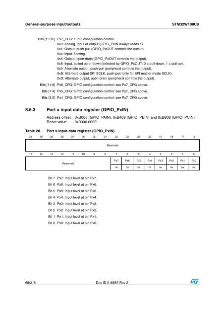
8.5.3 Port x input data register (GPIO_PxIN)<br />
Table 28.<br />
Address offset: 0xB008 (GPIO_PAIN), 0xB408 (GPIO_PBIN) and 0xB808 (GPIO_PCIN)<br />
Reset value: 0x0000 0000<br />
Port x input data register (GPIO_PxIN)<br />
31 30 29 28 27 26 25 24 23 22 21 20 19 18 17 16<br />
Reserved<br />
15 14 13 12 11 10 9 8 7 6 5 4 3 2 1 0<br />
Reserved<br />
Px7 Px6 Px5 Px4 Px3 Px2 Px1 Px0<br />
rw rw rw rw rw rw rw rw<br />
Bit 7 Px7: Input level at pin Px7.<br />
Bit 6 Px6: Input level at pin Px6.<br />
Bit 5 Px5: Input level at pin Px5.<br />
Bit 4 Px4: Input level at pin Px4.<br />
Bit 3 Px3: Input level at pin Px3.<br />
Bit 2 Px2: Input level at pin Px2.<br />
Bit 1 Px1: Input level at pin Px1.<br />
Bit 0 Px0: Input level at pin Px0.<br />
65/215 Doc ID 018587 Rev 2


