


Create successful ePaper yourself
Turn your PDF publications into a flip-book with our unique Google optimized e-Paper software.
General-purpose input/outputs<br />
<strong>STM32W108C8</strong><br />
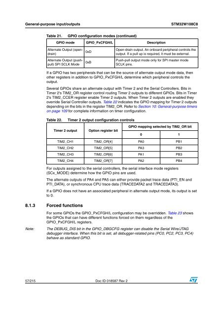
Table 21.<br />
GPIO configuration modes (continued)<br />
GPIO mode GPIO_PxCFGH/L Description<br />
Alternate Output (opendrain)<br />
Alternate Output (pushpull)<br />
SPI SCLK Mode<br />
0xD<br />
0xB<br />
Open-drain output. An onboard peripheral controls the<br />
output. If a pull up is required, it must be external.<br />
Push-pull output mode only for SPI master mode<br />
SCLK pins.<br />
If a GPIO has two peripherals that can be the source of alternate output mode data, then<br />
other registers in addition to GPIO_PxCFGH/L determine which peripheral controls the<br />
output.<br />
Several GPIOs share an alternate output with Timer 2 and the Serial Controllers. Bits in<br />
Timer 2's TIM2_OR register control routing Timer 2 outputs to different GPIOs. Bits in Timer<br />
2's TIM2_CCER register enable Timer 2 outputs. When Timer 2 outputs are enabled they<br />
override Serial Controller outputs. Table 22 indicates the GPIO mapping for Timer 2 outputs<br />
depending on the bits in the register TIM2_OR. Refer to Section 10: General-purpose timers<br />
on page 109 for complete information on timer configuration.<br />
Table 22.<br />
Timer 2 output<br />
For outputs assigned to the serial controllers, the serial interface mode registers<br />
(SCx_MODE) determine how the GPIO pins are used.<br />
The alternate outputs of PA4 and PA5 can either provide packet trace data (PTI_EN and<br />
PTI_DATA), or synchronous CPU trace data (TRACEDATA2 and TRACEDATA3).<br />
If a GPIO does not have an associated peripheral in alternate output mode, its output is set<br />
to 0.<br />
8.1.3 Forced functions<br />
Timer 2 output configuration controls<br />
Option register bit<br />
GPIO mapping selected by TIM2_OR bit<br />
0 1<br />
TIM2_CH1 TIM2_OR[4] PA0 PB1<br />
TIM2_CH2 TIM2_OR[5] PA3 PB2<br />
TIM2_CH3 TIM2_OR[6] PA1 PB3<br />
TIM2_CH4 TIM2_OR[7] PA2 PB4<br />
Note:<br />
For some GPIOs the GPIO_PxCFGH/L configuration may be overridden. Table 23 shows<br />
the GPIOs that can have different functions forced on them regardless of the<br />
GPIO_PxCFGH/L registers.<br />
The DEBUG_DIS bit in the GPIO_DBGCFG register can disable the Serial Wire/JTAG<br />
debugger interface. When this bit is set, all debugger-related pins (PC0, PC2, PC3, PC4)<br />
behave as standard GPIO.<br />
57/215 Doc ID 018587 Rev 2


