ON HIGH POWER IMPULSE MAGNETRON SPUTTERING
ON HIGH POWER IMPULSE MAGNETRON SPUTTERING
ON HIGH POWER IMPULSE MAGNETRON SPUTTERING

You also want an ePaper? Increase the reach of your titles
YUMPU automatically turns print PDFs into web optimized ePapers that Google loves.
University of South Bohemia<br />
Faculty of Science<br />
Institute of Physics and Biophysics<br />
<strong>ON</strong> <strong>HIGH</strong> <strong>POWER</strong> <strong>IMPULSE</strong><br />
MAGNETR<strong>ON</strong> <strong>SPUTTERING</strong><br />
Habilitation Thesis<br />
by<br />
Vítězslav Straňák<br />
December 2011, Greifswald
The work described in this thesis has been performed at:<br />
University of South Bohemia<br />
Faculty of Science<br />
Institute of Physics and Biophysics<br />
Branišovská 31<br />
370 05 České Budéjovice<br />
Czech Republic<br />
E.M.A. University of Greifswald<br />
Faculty of Mathematics and Natural Sciences<br />
Institute of Physics<br />
Felix-Huasdorff Strasse 6<br />
174 89 Greifswald<br />
Germany<br />
Academy of Science of the Czech Republic<br />
Division of optics<br />
Institute of Physics, v.v.i.<br />
Na Slovance 2<br />
180 00 Praha 8<br />
Czech Republic
Acknowledgements<br />
I am happy that I can do what I really like in my professional carrier: to discover new<br />
phenomena of plasma physics. It would have not been possible without help, support and<br />
company of a great number of people. I would like to thank all of them at this point.<br />
In particular I have to express my gratitude to closest collaborators Prof. Rainer Hippler<br />
(University of Greifswald), Prof. Milan Tichý (Charles University in Prague), Dr. Zdeněk<br />
Hubička and Dr. Martin Čada (both Academy of Sciences of the Czech Republic). I am<br />
much obliged to them, not only for their professional help but also for personal support<br />
which turns our relations into friendship.<br />
Last but not least, I am deeply grateful to my wife Šárka for her personal support and<br />
encouragement. I can not forget to acknowledge unflagging optimism coming from our<br />
little daughters Viktorie and Terezie.<br />
The work has been financially supported through grants and projects of German<br />
(SFB, BMBF, DFG) and the Czech Republic (MSMT, GACR, TACR, GAAV) governments.
Contents<br />
Preface 2<br />
1 Introduction to HiPIMS discharges phenomena 5<br />
1.1 Definition of HiPIMS discharges . . . . . . . . . . . . . . . . . . . . . . . . 5<br />
1.2 Plasma target interaction - sputtering . . . . . . . . . . . . . . . . . . . . . 6<br />
1.3 Transportation processes in HiPIMS - deposition . . . . . . . . . . . . . . 7<br />
2 HiPIMS power supplies and discharge generation 10<br />
2.1 HiPIMS in reactive atmosphere . . . . . . . . . . . . . . . . . . . . . . . . 12<br />
2.2 Advanced HiPIMS systems . . . . . . . . . . . . . . . . . . . . . . . . . . . 13<br />
3 Diagnostics of HiPIMS discharges 17<br />
3.1 Methods of plasma diagnostics . . . . . . . . . . . . . . . . . . . . . . . . . 17<br />
3.2 Properties of non-reactive HiPIMS discharges . . . . . . . . . . . . . . . . 19<br />
3.2.1 Time-resolved Langmuir probe measurements . . . . . . . . . . . . 19<br />
3.2.2 Time-resolved optical emission spectroscopy . . . . . . . . . . . . . 22<br />
3.2.3 Ion and power fluxes towards substrate . . . . . . . . . . . . . . . . 26<br />
3.2.4 Ion energy in HiPIMS discharges . . . . . . . . . . . . . . . . . . . 28<br />
3.3 Properties of reactive HiPIMS discharges . . . . . . . . . . . . . . . . . . . 30<br />
3.3.1 Estimation of negative (oxygen) ion density . . . . . . . . . . . . . 32<br />
4 HiPIMS for thin films deposition 37<br />
4.1 Deposition of photocatalytic TiO x films . . . . . . . . . . . . . . . . . . . . 37<br />
4.2 Effect of nitrogen doping on formation of TiO x N y . . . . . . . . . . . . . . 41<br />
4.3 Deposition of functional metallic Ti-Cu films . . . . . . . . . . . . . . . . . 44<br />
4.3.1 Formation of Ti-Cu films . . . . . . . . . . . . . . . . . . . . . . . 45<br />
4.3.2 Copper release from Ti-Cu films . . . . . . . . . . . . . . . . . . . . 47<br />
4.3.3 Effect of copper on cell and bacteria growth . . . . . . . . . . . . . 48<br />
4.4 Size-controlled formation of Cu nanoclusters . . . . . . . . . . . . . . . . . 50<br />
4.4.1 Effect of pulses on cluster formation . . . . . . . . . . . . . . . . . . 51<br />
4.4.2 Cluster mass and cluster particle flux . . . . . . . . . . . . . . . . . 53<br />
5 Conclusion 55<br />
References 56<br />
List of own publications related to the topic 61<br />
1
Preface<br />
Plasma physics and plasma based technology applications have made large progress in recent<br />
years [1,2]. Energetic particles, which occur in the plasma 1 volume, initiate unique<br />
physical and/or chemical reactions that can be realized only hardly at ordinary conditions.<br />
Among others applications plasma discharges have become an effective tool for plasmaassisted<br />
deposition of thin films with typical range of thickness from nanometers to units<br />
of micrometers (∼10 nm-10µm) [2]. These thin films are highly required in different<br />
areas of micro- and nanotechnology and can be utilized in micro-electronic, bio-medicine<br />
and optical coating industry. Further, the thin films can serve as protective layers (with<br />
mechanical or electrical features) as films with unique properties (ferrolectrics, ferromagnetics)<br />
or decorative coating. Because of various possible applications a wide variety of<br />
plasma-based methods for elemental and/or compound thin films have been invented [5].<br />
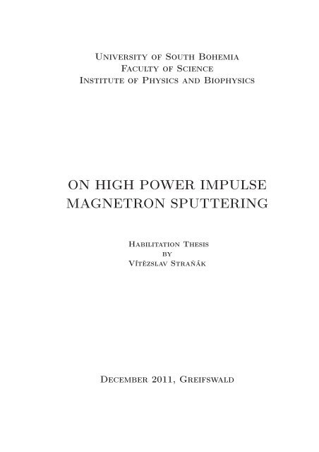
electron trap region<br />
B<br />
E<br />
E x B drift path<br />
target<br />
erosion rill<br />
S<br />
N<br />
S<br />
N<br />
S<br />
N<br />
photo of Cu discharge (diameter 50 mm)<br />
outer<br />
magnet<br />
water<br />
cooling<br />
inner<br />
magnet<br />
-V C<br />
cathode<br />
insulator<br />
sputtered Cu target (diameter 50 mm)<br />
Fig. 1: Planar magnetron sputtering. Planar circular magnetron sputtering is based on crossed magnetic<br />
and electric fields E×B. Buffer gas ions, produced in the "electron trap region", cause sputtering of<br />
target made from the material to be deposited.<br />
Physical vapor deposition (PVD), using the ion sputtering effect, is one of the most<br />
often used plasma assisted deposition methods [6]. The principle of ion sputtering is<br />
based on positive ions bombardment of a negatively biased target (cathode) made from<br />
the material to be deposited. Impinging of energetic ions results in ejection of target atoms<br />
which condense on a substrate forming a thin film [7]. This most simple process is called<br />
1 The term plasma was first introduced by Tonks and Langmuir in 1929 [3]. Chen defined plasma<br />
as electrically quasi-neutral gas of charged and neutral particles which exhibits collective behaviour [4].<br />
Plasma quasi-neutrality is meant in sense that one can assume for single charged particles n e ≈n i , where<br />
n e andn i denote electron and positive ions density, respectively. The particles can be in different quantum<br />
states - can be excited or de-excited to and from various energy levels. During these processes photons<br />
and subsequently light are produced. Collective behaviour means that not only local properties but also<br />
plasma conditions in remote regions influence plasma particles.<br />
2
diode sputtering. To increase the production of ions in plasma volume, i.e.to enhance the<br />
number of ions impinging on the target, the diode sputtering was modified by additional<br />
external magnets placed behind the cathode/target. The external magnetic field B is<br />
parallel (at least locally) to the cathode (i.e. perpendicular to electric field E) and forms<br />
an electron trap (E×B field drift), see Fig.1. This improved version, so-called magnetron<br />
sputtering 2 , was introduced first by Waits and Thornton in 1978 [8–11]. Despite theE×B<br />
electron confinement, the conventional dc-magnetron discharge is sustained mainly close<br />
the target and the ionization degree and ion flux rapidly decreases outwards from the<br />
cathode/target [12].<br />
The flux of ions and energetic particles towards the substrate plays an important role<br />
during deposition of thin films [13,14]. The microstructure and morphology of films is<br />
significantly influenced by energetic conditions on the top of layer surface. Since the<br />
ionization of sputtered metal atoms in dc-magnetron discharges is low (typically < 1%)<br />
the majority of ions hitting the substrate is represented by buffer gas 3 ions Ar + [15,16].<br />
This fact may cause subplantation of Ar atoms into the film [17] which deteriorates its<br />
quality (lattice defects [18], residual stresses [19], low adhesion [20]). Hence, it is generally<br />
desired to increase the ionization level of sputtered particles in the discharge volume. In<br />
case that ionization of metal atoms is > 50% we usually talk about ionized physical vapor<br />
deposition (IPVD) [21]. For that reason conventional magnetron sputtering systems have<br />
been modified by addition of the RF electric field component [22], ECRionization [23],<br />
plasma confinement [24] or they were operated in pulse mode [25, 26] to increase the<br />
fraction of metal ions.<br />
The operation of magnetron discharges in pulsed regime with low repetition frequency<br />
and short pulse width leads to significant increase of ionization [25,26]. In the pioneering<br />
work by Kouznetsov et al. in 1999 [27], high power pulse magnetron sputtering was used<br />
for the first time for IPVD of Cu film. In this early work, 50µs pulses of rather high<br />
power (nominal peak power density p p >3kW/cm 2 ) provided ion flux higher by about<br />
two orders of magnitude (compared with dc magnetron) and ionization of metal species<br />
about 70%. Such type of pulsed discharges is called High Power Impulse Magnetron<br />
Sputtering (HiPIMS) 4 and it represents the last trend in magnetron deposition.<br />
It is shown in the paper by Sarakinos et al. [17] that roughly 3-4 publications per year<br />
related to HiPIMS were published in the period 1999-2004. After that time the number of<br />
publications rapidly increases (up to now it is expected that there are about 200 original<br />
papers). In 2010, the first annual International Conference on Fundamentals and Applications<br />
of HiPIMS was organized in Sheffield (UK). EU COST Action MP0804 [28], focused<br />
on highly ionized pulse plasma processes where the HiPIMS plays a key role, was estab-<br />
2 Magnetron sputtering is almost exclusively used for practical applications. The ion bombardment is<br />
insufficient (usually because of low plasma density) during the diode sputtering, which results in significant<br />
reduction of ejected atoms, i.e. lower deposition rate.<br />
3 Magnetron discharges are typically operated with Ar buffer gas. Argon is relatively cheap and<br />
available inert gas with higher mass which is important for sufficient sputtering.<br />
4 The original name was High Power Pulsed Magnetron Sputtering (HPPMS) which is still used in<br />
English speaking countries.<br />
3
lished in the same year. Such expansion of activities in HiPIMS area well demonstrates<br />
high interest of academia as well as industrial communities.<br />
This habilitation thesis is focused on fundamental aspects of HiPIMS discharges and<br />
their application for deposition of different thin films. The author of the thesis works in<br />
the field of HiPIMS from the very beginning (his first related work was published in 2006)<br />
and his home laboratory is well established in magnetron sputtering deposition processes.<br />
The basic aspects of HiPIMS and HiPIMS deposition processes are presented in the thesis<br />
in form of annotated summary of essential results obtained by the author of the thesis<br />
and his coworkers. These results have been already published in international journals<br />
after peer review and the offprints are attached to the thesis as its integral part; in the<br />
text they are cited using Roman numerical system, e.g. [IV]. However, these author’s<br />
outcomes are not presented separately but they are embedded into a deeper context of<br />
already published works (cited using Arabic numbers, e.g. [4]).<br />
The thesis is practically divided in four main chapters. The first one brings an introduction<br />
to the phenomena of HiPIMS discharges. The second chapter deals with facilities<br />
and systems used for generation of HiPIMS discharges. The third chapter is focused on<br />
time resolved diagnostic and the attention of the fourth chapter is paid to deposition of<br />
various thin films and their properties.<br />
4
1. Introduction to HiPIMS discharges<br />
phenomena<br />
The first conventional dc-magnetron sputtering deposition system, in a correct technical<br />
configuration, was presented in the seventies of the last century. Since then, numerous<br />
review papers, e.g. [29], and books, e.g. [10,11,30], have been published, where details<br />
can be found. However, here we point at least to the typical and most important features<br />
of dc-magnetron sputtering (dc-MS). The dc-MS discharges are usually operated at a<br />
nominal discharge current density of the order of i dc ∼10-100mA/cm 2 , which somewhat<br />
corresponds with power densities p dc ≤15W/cm 2 . At such conditions the ionization level<br />
is low with typical electron density level n e ∼10 14 - 10 15 m −3 at pressures about 1Pa [30].<br />
In plasma discharge volume, mostly atoms of buffer gas (Ar) are ionized, resulting in ion<br />
flux of about ζ∼0.1-1.0mA/cm 2 towards the substrate. Densities of above mentioned<br />
parameters represents (technical) limits which are hard to exceed in dc-MS. Further increase<br />
of discharge current leads to overheating of the magnets, melting of the target or<br />
to occurrence of arc especially during reactive sputtering when the target is covered by<br />
electrically insulating layer [31].<br />
1.1 Definition of HiPIMS discharges<br />
The HiPIMS discharges are operated in pulse regime with low repetition frequency<br />
(f ∼100Hz) and short pulse width (duty cycle is usually ≤1%) [16, 27,32–37]. Experimentally<br />
HiPIMS discharges are operated with the same facilities as dc-MS just only<br />
require pulse power supplies. Pulse operation with small duty cycles allows keeping mean<br />
discharge current I m and mean discharge power P m (i.e. the current and power averaged<br />
over the pulse period T) at similar or even lower values as in dc-MS to prevent target<br />
overheating. However, values obtained in the pulse are much higher according to the<br />
formula<br />
∫ T<br />
I m = 1 I d (t)dt, (1.1)<br />
T 0<br />
where I m is the mean discharge current and I d is the discharge current varying in time. In<br />
this way the pulse current density i p can reach several A/cm 2 and the target is loaded with<br />
pulse power density p p in the range of a few kW/cm 2 . The electron density measured in<br />
HiPIMS systems usually exceeds n e ∼10 18 m −3 [33,37], which is by about two-three orders<br />
of magnitude higher than in conventional dc-MS [30].<br />
5
So far, no official definition of HiPIMS has been given. In general, pulse magnetron discharges<br />
which exceed pulse power density p p ≥1.0kW/cm 2 are considered as HiPIMS 1 [17].<br />
Further, the HiPIMS can be differentiated according to the pulse duration to groups with<br />
regular (50-200µs), short (1-20µs), large (200-400µs) and X-large (400-4000µs) pulse<br />
widths. The discharge breakdown through the ionizing collision cascade needs some time<br />
to propagate, which causes delay of discharge current after the cathode voltage onset typically<br />
observed in discharges with regular pulse width [27,38]. The delay between voltage<br />
and current is influenced by pressure, frequency, pulse current, etc [38].<br />
Short HiPIMS pulses used in combination with secondary plasma source decrease the<br />
voltage-current delay [39–41]. The secondary discharge provides pre-ionization of electrons<br />
that respond to fast increase of cathode voltage. Low dc-voltage or low power<br />
RF discharges used to be employed to achieve pre-ionization effect. Low power "background"<br />
discharges also sustain certain level of ionization which allows steady operation<br />
without arc [42,43]. Large pulse-width discharges, operated at very low frequencies, attain<br />
high pulse power densities; p p =10kW/cm 2 is reported in [44]. Long pulse widths<br />
allow the discharge to evolve into the metal discharge phase. In this phase the discharge is<br />
sustained by self-sputtering [44], i.e. the sputtering is mostly provided by metal ions and<br />
the discharge can sustain, in principle, even without Ar + sputtering (see next section).<br />
1.2 Plasma target interaction - sputtering<br />
Plasma target interaction and particle transportation are the key parameters during deposition<br />
process. Hence, this area has considerable importance and has been studied in<br />
several papers [17,44,45]. In next paragraphs only a brief summary of sputtering and particle<br />
transportation in non-reactive discharges is presented. The steady state and regular<br />
magnetron operation producing plasma is assumed at the beginning. The positive ions<br />
presented in plasma volume are accelerated towards negatively biased cathode/target.<br />
The ions hitting the target surface cause two processes: (i) production of secondary electrons<br />
and (ii) sputtering of target atoms. The secondary electrons are repelled from the<br />
cathode, gain energy from the cathode dark space, and enter the plasma, where they<br />
ionize the buffer gas to produce ion-electron pairs. The most intensive production of<br />
ions occurs in the region of "electron trap" where E and B are perpendicular, see Fig.1.<br />
Closed E×B drift path leads to Hall current which may be even higher than the discharge<br />
current itself [8,10]. Hence, secondary electrons are crucially important since they<br />
initiate the buffer gas ionization.<br />
Ion-induced potential electron emission (PEE) yield from the target surface can be<br />
expressed by semi-empirical equation [44–46]<br />
γ SE = 0.032(0.78E i −2φ), (1.2)<br />
1 Other HiPIMS definition says: As HiPIMS are considered discharges, the pulse power density of<br />
which is increased about two orders of magnitude due to operation in pulse mode if the averaged values<br />
are the same like in dc-MS.<br />
6
where E i is the ionization potential of arriving ions and φ denotes the work function of<br />
sputtered material; in Eq.(1.2) the kinetic emission is neglected [45] since the ion kinetic<br />
energy (even at HiPIMS conditions) is relatively low ≪ 300eV. Looking closer to the<br />
first ionization potentials and work functions (summarized in [44] for HiPIMS related<br />
processes and generally listed in [47]), it is obvious that secondary electron emission can<br />
not be caused by any singly charged metal ions. In other words, the secondary electrons,<br />
necessary for discharge operation, are provided only by Ar + ions or by multiply charged<br />
metal ions [45]. Only those ions have ionization energy high enough to fulfill the criterion<br />
resulting from Eq.(1.2) 0.78E i >2φ, providing potential emission of secondary electrons<br />
from the target. Hence, the discharge is sustained mainly due to bombardment of buffer<br />
gas ions Ar + at early stage of the pulse. Self-sustained self-sputtering in HiPIMS, i.e.<br />
operation of discharge without necessary support of gas ions, may occur later when doubly,<br />
and perhaps even higher, charged metal ions are present [44].<br />
The condition for self-sustained self-sputtering can be expressed by equation [45]<br />
α·β ·γ SS ≥ 1, (1.3)<br />
where α is the probability for the sputtered metal atom to be ionized, β is the probability<br />
for the metal ion to return to the target and γ SS denotes the yield of self-sputtering 2 .<br />
Usually the self-sputtering of the metals is about γ SS ≈1 for HiPIMS voltages about<br />
−1000 V [44, 47–49]. For this reason the probability coefficients α and β have to be<br />
high. Therefore, it can be assumed that in HiPIMS discharges there is larger fraction of<br />
multiply charged metal atoms which was also presented in several works [33,50,51].<br />
1.3 Transportation processes in HiPIMS - deposition<br />
Presence of charged metal particles in HiPIMS discharge affects the transportation processes<br />
and subsequently the deposition rate, too. These phenomena are studied in [52]<br />
and only main outcomes are summarized here. In the ideal case the deposition rate a d<br />
should be equal to target erosion rate Φ. However, due to losses in the discharge volume<br />
(diffusion towards the wall, ionization etc.) the deposition rate is usually lower: a d ≪Φ.<br />
The target erosion rate is proportional to discharge current j i , i.e. the number of ions<br />
impinging the target surface, and regarding the sputtering yield γ can be expressed by<br />
the equation<br />
Φ = j i ·γ(E). (1.4)<br />
As expressed by Eq. (1.4), the sputtering yield is a function of ion bombarding energy<br />
E =q·e·V C where q is the charge state of ion, e is the elementary charge and V C denotes<br />
2 The sputtering yield represents the number of target atoms sputtered (ejected from the target) per<br />
energetic particle striking the target with a kinetic energy. The sputtering yield is a function of ion kinetic<br />
energy and mass, incident angle and the material to be sputtered. Self-sputtering denotes the process at<br />
which target bombarding ion is formed from already sputtered (target) atom.<br />
7
the cathode voltage [48, 49]. The sputtering yield dependence on the projectile (ion)<br />
energy is described by [53]<br />
γ ∝ E m with m < 1. (1.5)<br />
Taking the processes in HiPIMS into account, the erosion rate is equal to [52]<br />
Φ = j Ar+ ·γ Ar+ (E)+j M+ ·γ M+ (E)−j M+ . (1.6)<br />
The first term, j Ar+ γ Ar+ (E), of Eq. (1.6) represents the target erosion caused by gas ion<br />
Ar + (typical and practically the only one sputtering initiator in dc-MS). The second part,<br />
j M+ γ M+ (E), denotes the self-sputtering provided by metal ion and the current −j M+<br />
represents re-directed metal ions, due to negative cathode potential, which are repeatedly<br />
"deposited" on the target (and cause the self-sputtering).<br />
It is a well known fact that deposition rate is lower in HiPIMS than in dc-MS [33,54].<br />
The first reason is that HiPIMS operate with higher voltages V C to get the same mean<br />
discharge power than dc-MS discharges [55]. SinceP m =I m·V C , the mean HiPIMS current<br />
has to be lower to get the same mean power. Because the discharge current is proportional<br />
to erosion rate, Eq.(1.6), the deposition rate decreases. The second reason of lower<br />
deposition rate is the fact that sputtering yield invoked by gas ion γ Ar+ is for most<br />
metals higher than the self-sputtering yield γ M+ [48,49]. Low self-sputtering yield plays<br />
important role because the ionization degree of metal particles in HiPIMS discharges is<br />
high > 90% [56,57]. Sarakinosetal. [52] expressed the HiPIMS-to-dc-MS ratio as:<br />
a H<br />
a ∝ (E) (E)−1<br />
· γAr+ · γM+ dc fAr+<br />
γ Ar+ (E 0 ) +fM+ γ Ar+ (E 0 ) , (1.7)<br />
wheref Ar+ andf M+ are relative fractions of Ar + and target M + ions, γ Ar+ (E) andγ M+ (E)<br />
are the sputtering and self-sputtering yields as a function of impinging ion energy, while<br />
γ Ar+ (E 0 ) is the sputtering yield at the reference dc-MS conditions, respectively.<br />
Transport of ionized metal particles in HiPIMS discharges strongly affects the deposition<br />
rate. It was observed experimentally that the ionization level and decrease of<br />
deposition rate are observed simultaneously [54]. In principle, the transport of (neutral)<br />
sputtered particles is determined by the velocity distribution and collisions with buffer<br />
gas atoms [10]. However, charged particles, it means also metal ions, are influenced by<br />
electric and magnetic field. It is known that the magnetic field is changed during the<br />
HiPIMS pulses [17, 58]. This phenomenon has not been fully understood yet and it is<br />
proposed that magnetic field is affected by (i) electron drift caused by applied magnetic<br />
field [58] and (ii) by electron drift caused by plasma pressure gradient and the gradient of<br />
magnetic field [59,60]. An important consequence is that the electron and ion transport<br />
affects each other mutually. As a result, a significant fraction of ions is transported radially<br />
away from the cathode. Hence, the ions are lost on the plasma chamber walls and<br />
the deposition rate decreases [59,61]. The side-wall loss of metal ions represents another<br />
important factor decreasing the deposition rate.<br />
8
Ratio of HiPIMS to dc-MS deposition rate as a function of metal atom ionization<br />
degree was derived first by Christie [62] and later extended by Vlcek et al. [57] to the<br />
form<br />
Π = (1−β)(1−χ+χξ i/ξ n )+β(1−σ)ξ i /ξ n<br />
, (1.8)<br />
1+βσ(γ Ar+ −γ M+ )<br />
where β is the ionization degree of sputtered atoms and σ is the fraction of ionized<br />
sputtered atoms re-directed back to the target. The main differences from the Eq. (1.7)<br />
are new parameters which represent the enhanced ionization in the discharge volume due<br />
to magnetic confinement of electrons χ and to transport parameters for the metal ions ξ i<br />
and neutrals ξ n employed as a relative ion-to-atom transport factor ξ i /ξ n [57].<br />
9
2. HiPIMS power supplies and<br />
discharge generation<br />
As already mentioned, HiPIMS systems differ from conventional dc-MS only by pulse<br />
controlled power supply equipment. A sputtering source itself is usually the same as<br />
in dc-MS processes. Typical planar magnetron sputtering source consists of a planar<br />
cathode usually parallel to anode 1 surface, see Fig.1. The cathode assembly consists of<br />
the source material, so-called target (made from the material to be deposited), directly<br />
connected with the backing power electrode. Magnets are placed below the backing<br />
electrode. Typical size of the cathode/target operated at laboratory condition 2 is usually<br />
between 25-150mm. The sputtering sources are mounted into the vacuum chamber, see<br />
Fig.2.1. The vacuum chamber can be equipped with several sputtering sources, e.g. for<br />
deposition of multi-structural film, composites, alloys etc.<br />
current density [A/cm 2 ]<br />
voltage [V]<br />
1.2<br />
0.8<br />
0.4<br />
0.0<br />
0<br />
-200<br />
-400<br />
-600<br />
<strong>ON</strong><br />
OFF<br />
O 2<br />
/Ar = 0.015<br />
O 2<br />
/Ar = 0.1<br />
O 2<br />
/Ar = 10<br />
p = 10 Pa<br />
f = 250 Hz<br />
V cathode<br />
V cathode+resistor<br />
p = 10 Pa<br />
f = 250 Hz<br />
O 2<br />
/Ar = 10<br />
0 50 100 150 200 250 300 350<br />
time [ s]<br />
Fig. 2.1: Schema of sputtering sources (red and<br />
green colored parts) mounted into the vacuum<br />
chamber.<br />
Fig. 2.2: Time evolution of peak discharge currents<br />
(upper panel) and voltages V C+R and V c .<br />
For our experiments we used to employ typical arrangement which can be met in<br />
many other laboratories. In our laboratory, the experiments have been carried out using<br />
commercial planar magnetron(s) situated in a stainless-steel vacuum chamber. The magnetron(s)<br />
is(are) equipped by the target(s) of 50mm or 75mm in diameter. The vacuum<br />
1 The anode is not strictly defined in MS discharges. It is usually the wall of the vacuum chamber<br />
or substrate holder which serves as an anode. In most cases the vacuum chamber is grounded while the<br />
substrate holder can be biased or can be floated.<br />
2 Rectangular or rotatable planar magnetron sputtering sources with larger sputtering area are used<br />
for industrial applications. See the information of producers, e.g. Gencoa Ltd.<br />
10
chamber is pumped out by a turbomolecular pump down to ultimate pressure of 10 −6 Pa.<br />
The working pressure in the chamber is adjusted by a throttle valve installed between the<br />
chamber and the turbomolecular pump. The flow rates of working gases employed during<br />
the process are controlled by mass flow controllers. Most of the experiments were done<br />
with typical flow rate of argon (20sccm) in a pressure range of 0.3-20Pa.<br />
A number of research groups have developed high-power pulsed supplies for generation<br />
of HiPIMS. These systems are more or less similar and they are based on a combination<br />
of dc-power supply loading a large capacitor bank of a pulsing unit connected to the<br />
magnetron cathode 3 . In our case, e.g. works [I-III], the capacitors are charged from dcsource<br />
AE Pinnacle 3000 during the idle part of the pulses. Stored energy is released<br />
in pulses activated by hand-made power switch based on IGBT transistors. The high<br />
power switch transistors are controlled by an external multi-channel pulse delay generator,<br />
Quantum 9518. The pulse delay generator serves also as trigger source for diagnostics<br />
tools. A ballast resistor serving as dummy load without magnetron discharge is inserted<br />
in series with the magnetron cathode path. The voltage waveforms measured over the<br />
ballast resistor by the oscilloscope can be used for calculation of discharge current using<br />
Ohm’s law, see Fig.2.2 lower panel. The other option is to use the current oscilloscopic<br />
probe and to measure the discharge current directly.<br />
current density [mA/cm 2 ]<br />
1000<br />
100<br />
10<br />
I V 7 dc-MS<br />
I V 6<br />
I V 2<br />
HiPIMS<br />
dc-MS<br />
HiPIMS<br />
mean discharge current [mA]<br />
750<br />
700<br />
650<br />
600<br />
550<br />
500<br />
450<br />
mean discharge current [mA]<br />
deposition rate [nm/min]<br />
p = 10 Pa, U = -580 V<br />
poissoned target<br />
1.4<br />
1.2<br />
1.0<br />
0.8<br />
0.6<br />
0.4<br />
0.2<br />
deposition rate [nm/min]<br />
400 600 800 1000<br />
cathode voltage [V]<br />
0.1 1 10<br />
ratio O 2<br />
/Ar<br />
Fig. 2.3: Comparison of current - voltage curves<br />
for dc-MS and HiPIMS discharges driven at similar<br />
conditions.<br />
Fig. 2.4: Dependence of deposition rate (right<br />
scale) and mean discharge current (left scale) on<br />
O 2 /Ar ratio.<br />
The voltage waveforms are practically rectangular and drop to zero when the active<br />
part of the modulation cycle finished, Fig.2.2. Slight delay of discharge current after<br />
the cathode voltage onset represents the time needed for propagation of ionizing collision<br />
cascade. In non-reactive mode, when the gas mixture ratio is very small, target voltage<br />
and the discharge current are linked by Thornton’s law [9]<br />
I ∝ V n . (2.1)<br />
3 From last two-three years the HiPIMS power supplies are also commercially available from<br />
Melec GmbH, Huttinger Electronic GmbH and Solvix SA.<br />
11
For dc-MS discharges, n takes on higher values (up to 15) while values close to one (usually<br />
from 1 to 3), i.e. I ∝V , are typical for HiPIMS [17]. Current-voltage characteristic of<br />
dc-MS and HiPIMS copper discharges at p=3Pa are compared in Fig.2.3. Slightly higher<br />
n in our HiPIMS is caused by lower range of applied target voltage. At certain target<br />
voltage -600V, n abruptly decreased due to loss of electron confinement. The similar<br />
behaviour was observed in [63].<br />
2.1 HiPIMS in reactive atmosphere<br />
Sputtering of elemental target in the presence of chemically reactive gases used to be<br />
called reactive sputtering [64]. Gases O 2 and N 2 are most frequently employed during<br />
reactive deposition of -oxide and -nitride films 4 , respectively. This phenomenon causes<br />
that surface of electrically conductive target is covered by insulating layer which results in<br />
hysteresis behaviour of cathode voltage [65,66]. The oxidized/nitrided target state is often<br />
called "poisoned" and is generally considered as unwanted state because it: (i) increases<br />
occurrence of arcs, (ii) decreases film quality due to ejection of micro-sized droplets [67]<br />
and (iii) reduces the deposition rate [I,III].<br />
The sputtering of poisoned target is more complex and other phenomena as sputtering<br />
yield of poisoning layer and its state have to be taken into account [I]. The effect of Ti target<br />
poisoned by O 2 (deposition of TiO 2 films) is clearly demonstrated in Fig.2.4. Presence<br />
of O 2 in the chamber increases the discharge current; the current density i p ∼1A/cm 2<br />
was measured in oxygen mixture O 2 /Ar=10. In this case the discharge current has almost<br />
linear dependence on time and reaches the highest value at the end of the active<br />
pulse. In O 2 /Ar=0.1 mixture the behaviour is different - i p reaches maximum faster but<br />
the maximum peak value of current density is lower despite the constant applied cathode<br />
voltage in both cases. These different waveforms are affected by the amount of O 2 and<br />
the explanation is as follows.<br />
Mean discharge current I m decreases when O 2 is delivered into the discharge, i.e. O 2<br />
decreases the discharge conductivity, see Fig.2.4. After reaching I m minima, near target<br />
poisoning O 2 /Ar∼0.1, I m increases almost linearly and attains original value. Such<br />
behaviour can be explained by the emission of secondary electrons induced by ion bombardment<br />
of the cathode/target (ISEE). Usually ISEE coefficient of Ti target decreases<br />
with oxidation. Abnormal behaviour observed in our case can be explained by a hypothesis<br />
given in [68], which is based on former works [69, 70]: the ISEE coefficient of the<br />
oxidized targets depends on the state of the formed oxide, i.e. a suboxide or fully oxide<br />
state. When a suboxide is formed, the ISEE coefficient is small. In contrast, if the target<br />
is fully oxidized, the ISEE ox coefficient is significantly larger than the ISEE m of the<br />
metal. Hence, after target oxidation the amount of electrons in the discharge increases<br />
4 As examples of oxide films we can list TiO 2 , ZnO, Al 2 O 3 , AZO (Aluminium-Zinc-Oxide), ITO<br />
(Indium-Tin-Oxide), BSTO (Barium Strontium Titanium Oxide) and many others. Nitrogen is added to<br />
the films to increase their hardness, typically TiN, or to get required semiconductor transition, eg. SiN x .<br />
12
due to ISEE but number of sputtered Ti particles/deposition rate is small because of low<br />
sputtering yield of oxides.<br />
In the same Fig.2.4 the dependence of deposition rate on O 2 /Ar ratio is shown, too.<br />
With negligible amount of oxygen the deposition rate reached about a d ∼15-20nm/min<br />
(not presented in the graph). Since the sputtering yield of titanium oxide is lower compared<br />
with pure titanium (Y TiOx =0.015 and Y Ti =0.3 for Ar + energy of 300eV [71,72]) at<br />
higher O 2 /Ar ratio (0.005
100 s<br />
V Ti<br />
HiPIMS<br />
V<br />
MF<br />
pulsed<br />
C p<br />
R p<br />
100 s<br />
V Cu<br />
HiPIMS<br />
R H<br />
- -<br />
C R<br />
V H<br />
DC<br />
H<br />
R s R s<br />
Ti Cu<br />
R H<br />
R H<br />
C H<br />
V DC<br />
L1<br />
L2<br />
+ +<br />
Fig. 2.5: The electric scheme of hybrid-dual-HiPIMS sputtering system with closed magnetic field.<br />
The electrical circuit is based on parallel combination of two identical pulsed power circuits L1 and L2.<br />
Each circuit consists of dc power supply V DC , power switches with large capacitors C H , and sputtering<br />
sources with opposite magnet polarity. Resistors R H serve as ballasting resistors. The mid-frequency<br />
circuit is connected to cathode via a step-down transformer. Configuration without MF-circuit is called<br />
dual-HiPIMS and was developed in our laboratory before, see [V].<br />
The potential of the electrode which acts as an anode is typically close to ground potential<br />
≈ 0 V, i.e. close to potential of the chamber which serves as a reference electrode. In<br />
that way the sputtering process of dual-HiPIMS is electrically and magnetically confined<br />
since the polarity of the magnets is reversed. The HiPIMS process parameters can be<br />
controlled separately for each loop because they are fully independent. This option, to<br />
apply different cathode voltages, is a main feature of the developed dual-pulse system for<br />
deposition of multi-component films with defined chemical composition 6 .<br />
Potentials measured on the Ti (ϕ Ti ) and Cu (ϕ Cu ) electrodes with respect to the<br />
ground are shown in Fig.2.6. The potential drop on the electrode which serves as cathode<br />
is fast with leading edge delay ∼ 5 ns. Sputtering voltages (V s = |ϕ Ti - ϕ Cu |) were set<br />
to keep the mean discharge currents constant I H m−Ti = 400 mA and I H m−Cu = 300 mA.<br />
Because of short time HiPIMS pulses, high peak current density i H p−Ti ≈2.75A/cm2 for Ti<br />
HiPIMS discharge andI H p−Cu≈2.25A/cm 2 for Cu HiPIMS discharge were measured. Such<br />
6 In our laboratory Ti-Cu films are often deposited. However, Cu and Ti has quite different sputtering<br />
yields (Y Ti = 0.4 and Y Cu = 2 for Ar + energies of 500 eV) [48]. For that reason the HiPIMS loops are<br />
controlled separately with different current/power densities to eliminate the different sputtering yields.<br />
14
values correspond to pulse power densities p H p ∼1kW/cm2 and pulse currents I H p ∼55A,<br />
respectively.<br />
Mid-frequency voltage source of V MF is connected in parallel to dual-HiPIMS driven<br />
electrodes separated by a transformer. The winding ratio of employed transformer is stepdown<br />
which prevents primary part of MF-circuit against penetration of HiPIMS pulses,<br />
i.e.protects mid-frequency source. The capacitor C P placed in the primary MF-circuit<br />
serves as a filter for dc-component of the mid-frequency source. Ballasting resistors R S<br />
have a minimum inductance. In our experiments, the mid-frequency source AC-PMP1<br />
Hüttinger Elektronik was operated with repetition frequency f M =94kHz and pulse width<br />
T M a =3µs while the dual-HiPIMS uses f H =100Hz and T H a =100µs.<br />
0<br />
0<br />
potential [V]<br />
peak current [A]<br />
-200<br />
-400<br />
-600<br />
-800 60<br />
MF<br />
45<br />
30<br />
15<br />
0<br />
(9950)<br />
Ti HiPIMS<br />
Ti HiPIMS<br />
dual-HiPIMS<br />
Cu HiPIMS<br />
dual-HiPIMS:<br />
f = 100 Hz<br />
T a<br />
= 100 s<br />
T d<br />
= 15 s<br />
HF discharge:<br />
f = 94 kHz<br />
T a<br />
= 3 s<br />
T d<br />
= 7 s<br />
Cu HiPIMS<br />
p = 3.0 Pa<br />
0 50 100 150 200 250<br />
time [ s]<br />
HiPIMS pulses<br />
potential [V]<br />
peak current [A]<br />
-200<br />
-400<br />
0.6<br />
0.4<br />
0.2<br />
0.0<br />
Ti electrode<br />
Cu electrode<br />
MF discharge:<br />
(driven together with dual-HiPIMS)<br />
f = 94 kHz<br />
T a<br />
= 3 s<br />
T d<br />
= 7 s<br />
p = 3.0 Pa<br />
260.3 262.3 264.3 266.3 268.3 2610.3 27<br />
time [ s]<br />
MF pulses<br />
Fig. 2.6: The time evolution of cathode voltage (upper panel) and discharge current density (lower panel)<br />
in hybrid-dual-HiPIMS during sputtering of Ti and Cu targets. Left: time evolutions during the dual-<br />
HiPIMS pulses (Im−Ti H = 400 mA, IH m−Cu = 300 mA. Right: evolution of MF discharge ITi,Cu<br />
m−M<br />
≈ 250 mA<br />
driven in the idle part of HiPIMS frequency.<br />
The MF - potentials applied on electrodes and MF - current densities are shown in<br />
Fig.2.6, too. The potential pulses on electrodes are not rectangular but look more<br />
like triangular outputs. The deformation is partially caused by the power supply itself,<br />
which does not give ideal rectangular output. Pulse discharge current reaches the value<br />
Ip−Ti,Cu M ≈600mA, which corresponds to peak power density pM p ∼13W/cm2 . It can be<br />
seen in Fig. 2.6 that applied MF potential does not appear symmetric immediately after<br />
the end of (Cu) HiPIMS pulses; the Cu MF potential amplitudes increase gradually while<br />
the Ti MF potential operates regularly after the end of Cu HiPIMS pulse. We believe<br />
that this asymmetry is caused by the (i) transient effect in sheath capacitance created at<br />
the electrode region and by (ii) plasma resistivity. The amount of charged particles in the<br />
cathode sheath region is always higher in comparison with anode region in this transient<br />
time. Hence, the potential drop of MF voltage is higher at the anode (Ti) than at the<br />
15
cathode (Cu) relative to the ground potential. The plasma potential at the cathode, at<br />
the end of HiPIMS pulse, is usually several volts, i.e. very close to ground potential [III].<br />
Combination of MF and HiPIMS discharges increases the deposition rate (in our experiments<br />
the deposition rate was increased several times). Nevertheless, the most important<br />
effect of MF discharge in a hybrid system is pre-ionization. MF-discharge produces certain<br />
amount of electrons that respond by fast increase of HiPIMS voltage. This not only allows<br />
faster development of HiPIMS pulses but also affords opportunity of significant pressure<br />
reduction in the vacuum chamber. Under our experimental conditions the hybrid discharge<br />
is stable at p=0.3Pa. If "pure" dual-HiPIMS is operated without MF support,<br />
the pressure has to be higher than p≥1.1Pa. However, the pressure reduction demands<br />
lower cathode voltage (in our case the cathode voltage has to be decreased roughly about<br />
-150V) to keep the same discharge current. A similar effect of reduced pressure during<br />
the HiPIMS process due to assisted MF-driven discharge was reported in [84,85]. This<br />
effect is associated with the presence of charged particles. The assistance of electrons left<br />
from the previous pulse in the plasma re-ignition was studied for MF discharges by Welzel<br />
et al. [86,87]. The pressure reduction is very important because it allows: (i) increase the<br />
purity grade of deposited films and (ii) control of the energy of incoming particles, which<br />
influences the film quality (the energy of particles is affected by collisions in discharge<br />
volume and is proportional to the mean free path length).<br />
16
3. Diagnostics of HiPIMS discharges<br />
HiPIMS pulses produce plasma characterized by the level of ionization, energy distribution<br />
of electrons, ions and neutrals, drift of particles and many other parameters. These<br />
properties are the key input quantities which influence complex processes in the plasma<br />
volume and subsequently growth of the thin films. Hence, the diagnostics of plasmas<br />
plays an important role in all experiments and becomes an inseparable part of plasmaassisted<br />
deposition. Knowledge of internal plasma parameters either serves for the study of<br />
elementary processes or helps to find optimal technological conditions. This section is an<br />
overview of HiPIMS plasma diagnostics during reactive as well as non-reactive sputtering.<br />
The comprehensive plasma characterization is reached because of combination of timeresolved<br />
Langmuir probe measurements, optical emission spectroscopy, ion flux and ion<br />
energy resolved investigations.<br />
3.1 Methods of plasma diagnostics<br />
The probe diagnostics of low temperature plasma, developed by Langmuir and Mott-Smith<br />
in twenties of last century [88], belong to the oldest as well as most often used diagnostic<br />
methods; comprehensively described in [89]. Distribution of electron energy is one of<br />
the most important parameters which are usually determined from IV characterictics<br />
measured by Langmuir probe. The second derivative of the measured probe current i<br />
with respect to probe potential V in transition region yields the so-called Druyvesteyn<br />
formula [90]<br />
f (ε) = 4 √ me<br />
e 3 A p 2<br />
√ d 2 i e ε<br />
dV 2, (ε = −eV). (3.1)<br />
Here ε =m e v 2 /2 is the electron energy, A p is the probe surface, i e denotes the electron<br />
current and V =V p -V pl , where V p and V pl represents probe and plasma potentials, respectively.<br />
Because of further processing, it is necessary to know whether EEDF is Maxwellian<br />
or not. The Maxwellian distribution function is described<br />
f maxwell (ε) = 2 √ π<br />
n e (kT e ) −3/2√ εexp<br />
( −ε<br />
kT e<br />
)<br />
, (3.2)<br />
and it is characterized by electron temperature T e and electron density n e . Low-pressure<br />
discharges has often the electron energy distribution that departs from a Maxwellian one.<br />
It can be easily distinguished by the second derivative of IV characteristic in transition<br />
area; the (d 2 i e /dV 2 ) of Maxwellian distribution is linear to ε (voltage) in semi-logarithmic<br />
17
scale. The Electron Energy Probability Function (EEPF) F(ε)=ε −1/2 f(ε) is sometimes<br />
introduced instead of EEDF [91]:<br />
F (ε) = ε −1/2 f(ε) = 4 √ me<br />
e 3 A p 2<br />
d 2 i e<br />
dV 2.<br />
(3.3)<br />
Assuming Maxwellian distribution, the electron temperature can be estimated from<br />
the inverse slope of the logarithmic electron probe current with respect to probe voltage<br />
(in volts)<br />
[ ] −1<br />
dlogie (V)<br />
T e = . (3.4)<br />
dV<br />
The non-Maxwellian plasmas can not be characterized by electron temperature and, instead,<br />
the mean electron energy E m has to be determined using EEDF<br />
E m = 〈ε〉 = 1 ∫∞<br />
n e<br />
0<br />
εf (ε)dε. (3.5)<br />
The effective temperature defined as T eff =2/3〈ε〉 is a suitable characteristic for non-<br />
Maxwellian plasma. For Maxwellian plasma T eff =T e .<br />
It is possible to estimate the electron density n e directly from EEDF, Eq.(3.1), too.<br />
The method is based on integral evaluation<br />
n e =<br />
∫∞<br />
0<br />
f (ε)dε. (3.6)<br />
However, the results are burdened by larger computational error caused by inaccurate<br />
estimation of (i) f(ε)∼d 2 i/dV 2 especially at low energies and (ii) definition of proper<br />
integral limits.<br />
There exists also other method how to determine the electron density directly employing<br />
only electron current [89] to reduce the computational error. According to the orbit<br />
motion limit regime [92], the electron current in the electron acceleration region should<br />
be square-root dependent on the V p , referenced to the V pl . Hence, the slope of i 2 e vs.V<br />
plot is proportional to n 2 e and the electron density can be determined from<br />
∆i 2 e<br />
∆V = 2 e<br />
π 2A2 p n 2<br />
m<br />
e. (3.7)<br />
e<br />
Using Eq.(3.7) the n e is computed directly from the probe data, no other quantities as<br />
T e being required. Thus the computational error is reduced to a minimum.<br />
Ion Velocity Distribution Function (IVDF) can be estimated from characteristics of<br />
ion current measured with respect to barrier potential in the so-called Retarding Field<br />
Analyzer (RFA) measurements [93, 94]. Let us consider a velocity distribution f(v,r)<br />
of ions where v =(v x ,v y ,v z ,) and r =(r x ,r y ,r z ,) represent the velocity and space vectors,<br />
respectively. In case of a homogeneous velocity distribution in the plane x-y, the partial<br />
18
integration over all v x and v y reduces f(v,r) to a one dimensional distribution f(v z ). In<br />
case of almost perfectly anisotropic velocity distribution with respect to the z-axis the<br />
IVDF is described by the formula [95,96]:<br />
f(IVDF) = − m e 2 ·<br />
1<br />
· dI c(ϕ r )<br />
, (3.8)<br />
T g A 0 dϕ r<br />
where m represents the mass of ions, T g is the total geometrical transparency of grids, A 0<br />
is the total open area of the entrance orifice, e denotes elementary charge andI c introduces<br />
detector current versus the applied retarding grid potential ϕ r .<br />
However, the RFA device is not usually equipped with mass selector, i.e. the measured<br />
I c is the total sum of all ion contributions. This makes data interpretation more difficult<br />
since magnetron sputtering discharge is a complex system of gas and metal ions which can<br />
not be distinguished by RFA. Because we want to avoid errors and confusing elements,<br />
the first derivative dI c (ϕ r )/dϕ r is called IVDF, presented as a function of energy E in<br />
arbitrary units, since f(IVDF)∝dI c (ϕ r )/dϕ r . Energies E in graphs 1 are calculated using<br />
E =eϕ r . Only single, elementary charged, ions are assumed using Eq.(3.8). To calculate<br />
Ion Energy Distribution Function (IEDF) from RFA measurements is more difficult and<br />
can significantly increase an error. However, the difference between IVDF and IEDF is<br />
carefully presented in [97,98].<br />
3.2 Properties of non-reactive HiPIMS discharges<br />
3.2.1 Time-resolved Langmuir probe measurements<br />
The mechanism of HiPIMS plasma ignition is similar to breakdown of an insulating material.<br />
The process starts with free electrons 2 accelerated outwards from the negatively<br />
biased cathode. The accelerated electrons collide with neutral gas which can cause electron<br />
impact ionization<br />
(e)+Ar −→ Ar + +e+(e), (3.9)<br />
producing gas ions and free electrons. The ions are attracted by the cathode and cause<br />
sputtering while electrons collide with other neutral atoms. These effects result in gas<br />
breakdown and plasma launching. Because of high power density there is an enormous<br />
increase of charged particles in the HiPIMS pulse. Hence, the electron density, in close<br />
vicinity (a few centimeters) of the target, is high, n e ≈5·10 18 m −3 . Its time-evolution,<br />
obtained from Langmuir probe measurements, is shown in Fig. 3.1. High plasma density<br />
results from large amount of metal sputtered particles since it is proportional to ionizing<br />
1 One could claim that f(IVDF) should be plotted against v rather than against E. However, rescaling<br />
the abscissa using v =(2E/m) 1/2 is not possible because of different masses of different measured ions.<br />
Because the energy is usually expressed in terms of energy units eV, the discrepancy in reading f(IVDF)<br />
vs. E can be accepted [95].<br />
2 Free electrons are essential for discharge breakdown. They occur naturally due to background radiation<br />
or thermal energy.<br />
19
collision frequency. For such a high electron density the ionization mean free path is<br />
short and significant fraction of sputtered atoms is ionized; e.g. the fraction of ionized Ti<br />
atoms was estimated about 90-99% [99]. The increase of n e usually corresponds with the<br />
evolution of peak discharge current reaching maximum typically at the end of the pulse.<br />
Exponential decrease of electron density follows after the pulse end.<br />
electron density [10 18 m -3 ]<br />
5 electron density<br />
mean electron energy<br />
4<br />
3<br />
2<br />
1<br />
p = 3 Pa<br />
f = 100 Hz, duty 1%<br />
copper target<br />
0.1 0<br />
pulse width off<br />
0<br />
0 50 100 150 200<br />
A [us]<br />
6<br />
5<br />
4<br />
3<br />
2<br />
1<br />
mean electron energy [eV]<br />
EEPF [eV -3/2 ]<br />
1<br />
0.1<br />
0.01<br />
dual HiPIMS - delay t d<br />
= 500 s<br />
f = 100 Hz, t a<br />
= 100 s<br />
Ti discharge ignated at t a<br />
= 0 s<br />
60 s<br />
100 s<br />
120 s<br />
250 s<br />
500 s<br />
0 2 4 6 8 10<br />
energy [eV]<br />
Fig. 3.1: The time evolution of electron density<br />
and mean electron energy in HiPIMS discharge,<br />
f = 100 Hz, p = 3 Pa.<br />
Fig. 3.2: Time evolution of Electron Energy probability<br />
Functions of Ti-HiPIMS pulse, f = 100 Hz,<br />
p = 3 Pa.<br />
Typical time evolution of mean electron energy E m is also shown in Fig. 3.1. The<br />
most energetic electrons are usually observed at early stage of HiPIMS pulse onset. After<br />
reaching maxima, E m steeply decreases which is caused by energy losses due to preferential<br />
ionization of sputtered metallic particles; ionization potential of metals (Cu + =7.73eV,<br />
Ti + =6.82eV) is significantly lower than the potential of buffer gas (Ar + =15.75eV). Metal<br />
sputtered particles produced at the onset of the pulse collide with electrons resulting<br />
in ionization. The density of metal atoms in the plasma gradually increases, which corresponds<br />
with decrease of E m .<br />
Time-evolution of Electron Energy Probability Function (EEPF) for Ti HiPIMS pulse<br />
is shown in Fig.3.2. The measurements were performed during a period of 60-500µs<br />
(let us to remind that the pulse width was 100µs). The Druyvesteyn EEPFs with broad<br />
energy distribution during the pulse to a double-Maxwellian distribution towards the end<br />
of the pulse and finally a Maxwellian-like distribution after the pulse are usually observed.<br />
Rapid cooling after the end of the pulse is typical. Cooling time is about 100µs during<br />
which the electrons lose half of their mean kinetic energy.<br />
The repetition frequency and duty cycle are key input parameters which influence<br />
plasma properties according to Eq.(1.1). Their effect on the electron density and electron<br />
energy was investigated in dual-systems during deposition of Ti-Cu film [V]. In this work<br />
dual-HiPIMS (f H =100Hz, duty 1%) and dual-MS (f D =4.65kHz, duty 45%) discharges 3<br />
3 Experimental arrangement of both systems can be found in chapter 2.2<br />
20
are compared. The highest electron density n H e−Ti ≈8·1018 m −3 was observed at the end<br />
of Ti pulse in dual-HiPIMS mode, see Fig.3.3. When the Cu discharge ignites, i.e. 15µs<br />
after the end of the Ti-pulse, the electron density shortly increases for a few microseconds<br />
but finally decreases down to the value n H e−Cu≈1·10 18 m −3 (n H e−Cu
high energy electrons dominate in bi-Maxwellian distribution. However, during a few<br />
microsecond, energy of fast electrons is reduced due to collisions in discharge volume and<br />
"cold" electron group become significant, having electron densities larger by about half<br />
an order of magnitude. Different electron groups were also detected in [100,101].<br />
3.2.2 Time-resolved optical emission spectroscopy<br />
The optical emission spectroscopy can qualify discharge properties and ionization level<br />
of sputtered particles. Time-averaged emission spectra for dual-MS and dual-HiPIMS<br />
discharges in UV-VIS wavelength range are compared in Fig.3.5. The atomic Ti and<br />
Cu emission lines dominate in the dual-MS working with higher repetition frequency.<br />
The dual-HiPIMS discharge shows similar spectral composition with additional emission<br />
of Ti + and Cu + . Presence of metallic (Ti + , Cu + ) ions in dual-HiPIMS is caused by<br />
higher plasma density which increases the probability of ionizing collisions and excitation<br />
of sputtered materials [56]. Intense emission of Ar lines was observed at wavelengths<br />
λ>650nm in both sputtering configurations. Because of much higher intensity emitted<br />
by Ar, the spectrum above 650nm is not included in Fig.3.5 [V].<br />
time [ s]<br />
normalized relative intensity [a.u.]<br />
2.0<br />
1.5<br />
1.0<br />
0.5<br />
0.0<br />
Cu<br />
Ti<br />
Cu<br />
Ti + Ti + Ti<br />
Cu Ti + Ti +<br />
Ti +<br />
Ti<br />
Ti<br />
Ti Ti<br />
dual HIPIMS<br />
f = 100 Hz, duty 1 %<br />
delay 15 s Ar<br />
Cu +<br />
300 350 400 450 500 550 600 650<br />
wavelength [nm]<br />
Ar +<br />
Ar +<br />
Ti<br />
Ti<br />
dual MS<br />
f = 4.65 kHz, duty 50 %<br />
delay 15 s<br />
Cu +<br />
Cu +<br />
normalized intensity [a.u.]<br />
0 50 100 150 200 250<br />
1.2<br />
0.9<br />
0.6<br />
0.3<br />
0.0<br />
0.9<br />
0.6<br />
0.3<br />
0.0<br />
dual HiPIMS<br />
dual MS<br />
Ti - <strong>ON</strong><br />
delay<br />
Cu - <strong>ON</strong><br />
OFF<br />
Ti<br />
Cu<br />
Ti +<br />
Cu +<br />
0 50 100 150 200 250<br />
time [ s]<br />
Fig. 3.5: Comparison of time-averaged spectra<br />
overviews emitted by dual-MS and dual-HiPIMS.<br />
Upper spectrum - dual-MS, lower spectrum - dual-<br />
HiPIMS.<br />
Fig. 3.6: Time evolution of particular line intens.<br />
for excited metals λ Ti = 453.3 nm, λ Cu = 324.7 nm<br />
and for λ Ti+ = 334.9 nm, λ Cu+ = 615.4 nm ionized<br />
metals.<br />
Selected spectral lines of neutral Ti (λ Ti =453.3nm), Cu (λ Cu =324.7nm) and of ionized<br />
Ti + (λ Ti+ =334.9nm), Cu + (λ Cu+ =615.4nm) metal elements are compared for dual-<br />
MS and dual-HiPIMS in Fig.3.6. The intensity evolutions of Ti line, observed for different<br />
sputtering modes, exhibit different behaviour. In dual-HiPIMS, the Ti intensity increases<br />
in two (nearly) linear steps. The intensity increases slightly during the first half of<br />
the Ti-pulse while a steep rise is observed for Ta−Ti H >50µs. Two-step evolution of Ti<br />
line intensity in dual-MS is observed, too. However, the first linear part is much shorter:<br />
22
oughlyTa−Ti D
elative intensity of Ar [a.u.]<br />
9<br />
6<br />
3<br />
0<br />
Ti - HiPIMS<br />
Cu - HiPIMS<br />
dual-HiPIMS<br />
hybrid-dual-HiPIMS<br />
dual-HiPIMS:<br />
f = 100 Hz<br />
T a<br />
= 100 s<br />
T d<br />
= 15 s<br />
HF discharge:<br />
f = 94 kHz<br />
T a<br />
= 3 s<br />
T d<br />
= 7 s<br />
p = 3.0 Pa<br />
= 811.5 nm (Ar)<br />
0 100 200 300<br />
time [ s]<br />
relative intensity Ti [a.u]<br />
7 Ti - HiPIMS Cu - HiPIMS<br />
6<br />
5<br />
4<br />
3<br />
2<br />
1<br />
0<br />
Ti, hybrid-DH<br />
Ti, DH<br />
Cu, hybrid-DH<br />
Cu, DH<br />
dual-HiPIMS:<br />
f = 100 Hz<br />
T a<br />
= 100 s<br />
T d<br />
= 15 s<br />
HF discharge:<br />
f = 94 kHz<br />
T a<br />
= 3 s<br />
T d<br />
= 7 s<br />
p = 3.0 Pa<br />
= 327.4 nm (Cu)<br />
= 453.3 nm (Ti)<br />
0 100 200 300<br />
time [ s]<br />
22<br />
19<br />
15<br />
11<br />
7<br />
4<br />
0<br />
relative intensity Cu [a.u.]<br />
Fig. 3.7: Time resolved optical emission measurements<br />
of Ar line λ Ar = 811.5 nm.<br />
Fig. 3.8: Time resolved optical emission measurements<br />
of λ Cu = 327.4 nm and λ Ti = 453.3 nm.<br />
the electrons. In this way the deposition rate on the substrate is reduced and the anode<br />
can be contaminated (covered) by the cathode material [VII]. Hence, some fraction of Ti<br />
vapour is deposited on the inactive Cu anode during the Ti-HiPIMS pulse and it has to<br />
be sputtered first at the beginning of the (second) Cu-HiPIMS pulse (and vice-versa for<br />
reversed polarity of Ti-Cu electrodes). The second source of the emission observed might<br />
be represented by ions still persisting in the cathode vicinity from previous pulse when it<br />
served as anode (see the explanation given above).<br />
A more probable explanation is the first one, based on target contamination. The<br />
reasons are as follows: A well-pronounced emission of different materials at the beginning<br />
of HiPIMS pulses is observable only for dual-HiPIMS mode despite the fact that the<br />
intensity of Cu emission at the beginning of the Ti pulse is much lower, see Fig.3.8<br />
(this effect corresponds with the low sensitivity of the iCCD chip which is needed for<br />
measurement of massive sputtering during the Cu-HiPIMS pulse). When the hybrid dual-<br />
HiPIMS discharge is operated, the emission of only Ti is observed during Cu-HiPIMS.<br />
The absence of Cu emission at the beginning of the Ti-HiPIMS pulse is caused by the<br />
operation of an MF-discharge in the idle time of HiPIMS pulses which provides a "cleaning<br />
effect".<br />
To study the discharge expansion dynamics and target contamination, the fast optical<br />
emission imaging was employed [IV,VIII]. Images for both Ti-driven (right side of images)<br />
and Cu-driven (left side of images) discharges in hybrid-dual-HiPIMS configuration are<br />
shown in Fig.3.9. The total light emission 5 is presented in Fig.3.9. The Ti-pulse is ignited<br />
first (T a =0µs) and the emission in the vicinity of Ti target is immediately detected. This<br />
5 Measurements with optical filters for particular (Ar, Ar + , Ti, Ti + , Cu, Cu + ) wavelengths were also<br />
done to verify the origin of imaged light emission. The function of automatic iCCD chip sensitivity adjustment<br />
was activated during all recording of time-resolved image sequences since the emission intensity<br />
dynamically varies in time. In other words, the iCCD chip sensitivity was adjusted automatically by the<br />
gain (G=1-255) of the amplifier to obtain optimal images.<br />
24
A<br />
G = 233<br />
T = 13 s<br />
Ti-HiPIMS pulse<br />
B<br />
G = 31<br />
T = 64 s<br />
Ti-HiPIMS pulse<br />
C<br />
G = 255<br />
T = 109 s<br />
HiPIMS pulse delay<br />
D<br />
G = 240<br />
T = 123 s<br />
Cu-HiPIMS pulse<br />
D<br />
G = 180<br />
T = 171 s<br />
Cu-HiPIMS pulse<br />
E<br />
G = 255<br />
T = 276 s<br />
Ti-MF pulse<br />
F<br />
G = 255<br />
T = 280 s<br />
Cu-MF pulse<br />
Fig. 3.9: Time resolved images of Ti-Cu hybrid-dual-<br />
HiPIMS discharge. Images: A and B - Ti HiPIMS pulse<br />
(0 - 100µs), C - delay between pulses (100 - 115µs), D and<br />
E-Cu HiPIMS pulse (115 - 215µs), F-MF pulse of Ti, G -<br />
MF pulse of Cu (MF driven in the idle time of HiPIMS). Ti<br />
magnetron is shown on the right and Cu on the left-hand<br />
side of images, respectively. The gain of iCCD amplifier G<br />
was automatically varied in range 0 - 255.<br />
light is mostly produced by Ar ∗<br />
(verified by measurements with<br />
optical filters and measurements<br />
with OES). However, after a few<br />
microseconds, T a ∼1-3µs, visible<br />
emission in neighborhood of Cu<br />
electrode is observed as well. It<br />
becomes more pronounced in the<br />
vicinity of Cu-target and creates<br />
well-defined bond between Cu (anode)<br />
and Ti (cathode), Fig.3.9 A.<br />
This effect is due to magnetic<br />
(reversed polarity of magnets)<br />
and electric (anode-cathode) confinements.<br />
Electrons, repelled<br />
from the cathode ϕ Ti ≃-800V<br />
(Fig.2.6), move along the magnetic<br />
field line towards the anode, due<br />
to |ϕ Ti - ϕ Cu | ∼ 800 V, and cause<br />
electron impact ionization of Ar<br />
gas. Apparent bonding between<br />
electrodes is somewhat similar to<br />
the edge of a virtual tubular-like<br />
anode of dual magnetron system.<br />
However, bounding between<br />
sputtering sources, represented by<br />
emission of Ar ∗ and Ar + , between<br />
electrodes disappears after<br />
full propagation of the Ti-HiPIMS<br />
pulse, see Fig.3.9 B. This is not<br />
true because the emission of sputtered<br />
Ti gradually exceeds the intensity<br />
of Ar ∗ and Ar + lines and<br />
the sensitivity of iCCD chip is automatically<br />
decreased. After 25-<br />
30µs, massive sputtering of Ti is<br />
dominant and a larger cloud is<br />
formed nearby Ti target. The<br />
cloud, formed mainly by neutral<br />
Ti and Ar (with some fraction of<br />
Ar + and Ti + ), propagates downwards<br />
with a speed roughly about<br />
2-3mm/µs. Measured speed some-<br />
25
what corresponds with the diffusion velocity; the diffusion coefficient of Ti in Ar atmosphere<br />
gives the velocity at discussed experimental condition about 1.5mm/µs. The<br />
situation is more complex since there is a strong production of (energetic) ions during<br />
HiPIMS pulses which are dragged due to ambipolar diffusion. Similar velocities of metal<br />
propagation in HiPIMS discharges were published elsewhere [104]. The movement could<br />
be also caused by drift (forcing the particle to move in a certain direction). Nevertheless,<br />
owing to the formation of a virtual tubular-like anode, we believe that fundamental drift<br />
currents flow between the electrodes due to electric and magnetic confinement. Hence,<br />
the drift in substrate direction is limited and we suppose that it is ambipolar diffusion<br />
which provides for the presence of ions in the substrate region.<br />
Fig.3.9C depicts the discharge between the HiPIMS pulses, i.e. time period 100-<br />
115µs. The discharge is not fully stable, which corresponds with voltage measured between<br />
the electrodes, see Fig.2.6. Despite instabilities, the emission appears in the Ti<br />
target vicinity and, weaker but still detectable, is observable near the Cu target, see<br />
Fig. 3.9C. Despite weak intensity of MF discharge in the delay between the HiPIMS<br />
pulses, the ions persist in the volume and support fast re-ignition of Cu-HiPIMS pulse.<br />
The sputtering yield of Cu is higher in comparison with Ti [48]. For that reason we can<br />
suppose intense sputtering of copper and its subsequent ionization. The effect of magnetic<br />
confinement is not as pronounced as in the case of Ti-HiPIMS pulse because of lower sensitivity<br />
of the iCCD chip. The last two images show MF-pulses: Fig. 3.9E sputtering of<br />
Ti and Fig. 3.9 F sputtering of Cu, respectively. The most important is that the emission<br />
is due to excited atoms Ar ∗ , Cu ∗ and Ti ∗ .<br />
3.2.3 Ion and power fluxes towards substrate<br />
High ionization degree of metal particles and their flux towards the substrate crucially<br />
influence film properties [105–108]. However, the degree of ionization n i /(n i +n n ) is not<br />
equal to ionized flux fraction ζ i /(ζ i +ζ n ) because the flux of ions is governed by electron<br />
temperature T e while the neutral flux by the gas temperature T g (T e ≫T g ). This means<br />
that the ion flux fraction is larger than the degree of ionization and therefore it is not<br />
uncommon to find that the ionized flux fraction at the substrate can be more than 90%<br />
although the degree of ionization reaches only about 50% [105,109]. Positive ion flux ζ i<br />
can be determined e.g. from measurements of ion currents on a planar probe biased by<br />
pulsed voltage 6 [110].<br />
Because of high ionization degree the ion flux is usually higher in HiPIMS than in<br />
mid-frequency or dc-MS discharges. The difference is shown in Fig.3.10 where ion fluxes<br />
of dual-HiPIMS and dual-MS are compared [V]. The highest ion flux ζ i ≈80mA/cm 2 was<br />
measured during Ti-HiPIMS pulse driven in dual arrangement, see Fig.3.10. High ion<br />
flux is a sum of all ion contributions (ζi<br />
Ar+ , ζi<br />
Ti+ or ζi<br />
Cu+ ) in the presented case. During<br />
the Cu-HiPIMS pulse the ion flux is slightly lower, which is caused by lower applied<br />
6 The angular frequency of the applied pulsed bias ω has to be significantly lower than the ion plasma<br />
frequency ω i . Due to the inequality ω < ω i , the ions instantly respond to the changes of substrate/probe<br />
voltage and the time evolution ζ i (t) can be determined precisely.<br />
26
power density and higher ionization potential of Cu, but still it is by about two orders of<br />
magnitude larger than the values obtained in dual-MS or fluxes reported elsewhere [110].<br />
The dependence of the mean ion flux, averaged over the pulse width, on substrate bias<br />
is shown in Fig.3.11. Ion flux depends nearly linearly on the bias voltage, but the flux<br />
from dual-HiPIMS is always significantly bigger ζ H i ≫ζ D i . Hence, biasing of the substrate<br />
during dc-MS or dual-MS somewhat increases ion flux but hardly can reach impact of<br />
HiPIMS.<br />
ion flux - dual MS [mA/cm 2 ]<br />
3.0<br />
Ti - <strong>ON</strong> Cu - <strong>ON</strong> pause dual HiPIMS<br />
dual MS<br />
dual HiPIMS<br />
2.5<br />
2.0<br />
1.5<br />
Ti - <strong>ON</strong> Cu - <strong>ON</strong> Ti - <strong>ON</strong> Cu - <strong>ON</strong><br />
dual MS<br />
1.0<br />
0 100 200 300 400<br />
time [ s]<br />
100<br />
80<br />
60<br />
40<br />
20<br />
0<br />
ion flux - dual HiPIMS [mA/cm 2 ]<br />
ion flux [mA.cm -2 ]<br />
140<br />
120<br />
100<br />
80<br />
2<br />
1<br />
dual HiPIMS<br />
dual MS<br />
0<br />
20 40 60 80 100 120 140 160<br />
probe bias [V]<br />
Fig. 3.10: Comparison of ion fluxes for dual-MS<br />
(two periods) and dual-HiPIMS (one period) to<br />
substrate/probe biased at U b = -30 V.<br />
Fig. 3.11: Averaged ion flux to the negatively biased<br />
substrate for different voltages. The graph<br />
clearly shows differences of two orders of magnitude.<br />
Ions are the most important contributors to the total power density flux. The total<br />
power flux somehow represents the total energy, coming from discharge, which affects<br />
the growing film. High power flux usually causes substrate heating which can damage<br />
thermally sensitive materials, e.g. plastics etc. Hence, it is generally wanted to obtain<br />
low power flux mostly represented by metal ions. In our case [V] the total power density<br />
flux, estimated from calorimetric probe measurements [111,112], is roughly twice larger in<br />
dual-HiPIMS (P H Γ =38mW/cm 2 ) than in dual-MS mode (P D Γ =17mW/cm 2 ). The energy<br />
fluxes of particular species (ions, electrons and neutral particles) can be estimated from the<br />
model derived in [78]. It was calculated, within computational error, that the major part<br />
of the power density flux to floating substrate is represented by charged particles; power<br />
density from ions ∼75% for dual-HiPIMS and ∼60% for dual-MS and power density<br />
from electrons ∼25% for both sputtering configurations of the total power density flux.<br />
The power density flux from neutral particles in dual-MS reaches about 10% while in<br />
dual-HiPIMS is nearly negligible (≤1%) because of high ionization.<br />
According to Gras-Marti’s and Valles-Abarca’s analytical model [113], more than 90 %<br />
of high-energy neutral particles (sputtered Ti, Cu atoms and Auger neutralized reflected<br />
Ar ions) will be thermalized before they reach the substrate surface and their energetic<br />
contribution to the substrate can be neglected. The validity of power density flux values<br />
27
estimated from the model can be demonstrated by their relative comparison with ion flux<br />
measurements. The ratio of ion fluxes ζi H /ζi D ≈32 and ratio of power density flux from<br />
ions is Pi H /Pi D ≈30.5. We can conclude that: (i) ion contribution dominates in power<br />
density flux, (ii) ion flux to substrate is nearly about two orders of magnitude higher<br />
in dual-HiPIMS than in dual-MS [V]. However, the deposition rate (i.e. the number of<br />
incoming particles onto substrate per time unit) is significantly lower in HiPIMS processes.<br />
Taking the lower deposition rate into account, a higher energy per incoming particle in<br />
HiPIMS has to be expected [114].<br />
3.2.4 Ion energy in HiPIMS discharges<br />
It was already mentioned in the previous chapter that ions are major carriers of energy<br />
towards the substrate in HiPIMS discharges. Time-resolved ion distribution functions,<br />
measured in hybrid-dual-HiPIMS discharge by retarding field analyzer (RFA) are presented<br />
in Fig.3.12 [IV]. Generally, we can say that typical energy of ions hitting the electrically<br />
isolated substrate is about ∼10 eV during HiPIMS pulses; ions gain the energy in the substrate/RFA<br />
detector sheath owing to difference between plasma and floating potentials.<br />
The maxima of IVDFs measured for the first Ti-HiPIMS pulse are slightly higher than<br />
for the second Cu-HiPIMS pulse. This can be explained by higher pulse power densities<br />
reached during Ti-HiPIMS pulse, since mean discharge currents were different.<br />
The IVDFs, measured during Ti-pulse, starts to develop roughly at T a ≈30µs. Most<br />
probably this behaviour corresponds with production and ambipolar diffusion of ions<br />
generated in the cathode region 7 . The diffusion rate of emission cloud, represented by<br />
excited atoms and ions, was estimated to about 2-3mm/µs from OEI measurements. This<br />
speed most probably pertain to ions (accelerated by ambipolar diffusion) while the neutral<br />
atoms are slower 0.5mm/µs at a pressure of 3Pa [102]. Since the distance between the<br />
RFA probe and magnetron cathode is 50mm in vertical direction, we can conclude that<br />
weak IVDFs in first microseconds are caused by absence of ions travelling from cathode<br />
towards the RFA sensor.<br />
The situation is more complex, since the detected ions are not created only in the<br />
vicinity of the target moving downwards due to the process of diffusion. Some ions can<br />
be created in the plasma bulk and can then reach the substrate area at the same time<br />
as fast ions travelling from the target. Further, ions of sputtered particles, together with<br />
argon ions, might move towards the substrate due to an ion-acoustic solitary wave, as<br />
reported in [115, 116]. However, because both targets are electrically and magnetically<br />
confined, a tubular-like virtual anode is formed between the magnetrons. Hence, ions<br />
are electrostatically forced to stay in the vicinity of the electrons and the effect of an<br />
ion-acoustic solitary wave moving towards the substrate is most probably limited in our<br />
case.<br />
7 There exist also some other (less probable) mechanisms which may be responsible for observed phenomena,<br />
e.g. production of secondary ions in discharge volume, effect of E×B drift, creation of ionizing<br />
avalanches etc. However, these effects have not been studied in detail as yet.<br />
28
IVDF<br />
3<br />
2<br />
1<br />
dual-HiPIMS:<br />
f = 100 Hz<br />
T a<br />
= 100 s<br />
T d<br />
= 15 s<br />
HF discharge:<br />
f = 94 kHz<br />
T a<br />
= 3 s<br />
T d<br />
= 7 s<br />
energy [eV]<br />
20<br />
10<br />
0<br />
dual-HiPIMS:<br />
f = 100 Hz<br />
T a<br />
= 100 s<br />
T d<br />
= 15 s<br />
HF discharge:<br />
f = 94 kHz<br />
T a<br />
= 3 s<br />
T d<br />
= 7 s<br />
0<br />
100<br />
200<br />
time [ s]<br />
300<br />
400<br />
-10<br />
0<br />
10<br />
20<br />
energy [eV]<br />
Ti-HiPIMS Cu-HiPIMS MF<br />
<strong>ON</strong> OFF<br />
-10<br />
0 50 100 150 200 250 300 350 400<br />
time [ s]<br />
3D projection<br />
2D projection<br />
Fig. 3.12: Time resolved measurements of IVDFs in hybrid-dual-HiPIMS discharge. Left panel: time<br />
resolved measurements presented in 3D graph. Right panel: the same data figured in 2D projection.<br />
Mean HiPIMS discharge currents Im−Ti H = 400 mA, IH m−Cu = 300 mA and mean MF-discharge currents<br />
≈ 250 mA were kept constant, p = 3.0 Pa.<br />
I M m<br />
Pre-ionization also increases the ion energy [IV], as illustrated in Fig.3.13. The figure<br />
shows a situation when only the first, Ti-HiPIMS, pulse is driven (zero potential is applied<br />
on Cu cathode) in hybrid configuration. The IVDFs during active Ti-HiPIMS pulse is<br />
nearly identical with measurements presented in Fig.3.12. Nevertheless, ions incoming<br />
with high energies (∼12eV) were detected also after the end of the HiPIMS pulse, which<br />
is probably caused by ambipolar diffusion motion, see above. Ions with lower energies<br />
(5eV) were observed at the same time (T ∼120µs), too, see Fig.3.13. This low energy<br />
peak originates from MF-discharge operation activated after Ti-HiPIMS pulse. Ion distributions<br />
of MF discharge occur regularly with period of ∼10µs (corresponding with MF<br />
frequency 94kHz) at T a ≥250µs. Afterwards, the MF-discharge is stabilized and produces<br />
ions with incoming energies of about 1-3eV, see Fig.3.13.<br />
Since the time of flight is given by the speed of the particle, we can easily deduce<br />
that the speed of 12eV ions will be 1.6 times higher then of 5eV ion. Furthermore, we<br />
can assume that Ti ions will comprise a substantial part of the 12eV ions and that their<br />
speed will be somewhat lower. On the other hand, 5eV ions comprise mainly Ar ions.<br />
We can conclude that the time of flight will be similar and differences will be negligible<br />
(i.e. speeds are approx. 6mm/µs versus 4.5mm/µs). Then we believe that ions created in<br />
plasma bulk or in the vicinity of the target during the Ti-HiPIMS pulse reach the analyzer<br />
at a distance of 50mm from the target face 10-20µs after the end of the Ti-HiPIMS pulse<br />
and are detected as a second peak in measured IVDF at the time T a ∼120µs.<br />
29
energy [eV]<br />
20<br />
10<br />
0<br />
Ti-HiPIMS<br />
<strong>ON</strong><br />
Cu-HiPIMS<br />
OFF<br />
dual-HiPIMS:<br />
f = 100 Hz<br />
T a<br />
= 100 s<br />
T d<br />
= 15 s<br />
HF discharge:<br />
f = 94 kHz<br />
T a<br />
= 3 s<br />
T d<br />
= 7 s<br />
MF<br />
-10<br />
0 50 100 150 200 250 300 350 400<br />
time [ s]<br />
IVDF [a.u.]<br />
2.0<br />
1.5<br />
1.0<br />
0.5<br />
p = 0.5 Pa<br />
p = 3.0 Pa<br />
p = 5.0 Pa<br />
time-averaged<br />
hybrid-dual-HiPIMS<br />
f HiPIMS<br />
= 100 Hz<br />
f MF<br />
= 94 kHz<br />
0.0<br />
0 5 10 15 20 25 30 35<br />
energy [eV]<br />
Fig. 3.13: Effect of hybrid mode on IVDFs formation.<br />
Only Ti-HiPIMS pulse was operated supported<br />
by regularly driven MF discharge. Pressure<br />
was kept constant, p = 3.0 Pa.<br />
Fig. 3.14: Time-averaged measurement of IVDF<br />
as a function of pressure in the chamber. The discharge<br />
was operated in hybrid-dual-HiPIMS mode.<br />
Other important effect of hybrid system is the possibility of reducing the working pressure.<br />
Since the MF discharge provides pre-ionization and supplies charged particles before<br />
HiPIMS pulses, the pressure can be reduced by more than one order of magnitude. The<br />
pressure affects the ion energy, shown in Fig.3.14, and it can be confirmed that (i) measured<br />
ion energy increases and (ii) full width at half maximum of IVDFs also increases<br />
with decreasing pressure. This behaviour is well known since the energetic losses due to<br />
collisions are lower at lower pressures. At low pressures we observed slightly pronounced<br />
double-peak distribution, see Fig.3.14. It is expected that the high energy peak is formed<br />
by ions during the HiPIMS-pulse whereas the low energy peak originates from the time<br />
after the end of the pulse [117,118] or might be caused by an effect of the difference in<br />
the time of flight for low and high energy ions generated simultaneously.<br />
3.3 Properties of reactive HiPIMS discharges<br />
Chemically reactive species, generated due to dissociation of reactive gases, lead to reactions:<br />
(i) in plasma volume, (ii) at the target surface and (iii) at coated surfaces. All these<br />
reactions are responsible for different behavior of reactive plasma sputtering. The overview<br />
spectrum of Ar/N 2 +O 2 HiPIMS discharge during sputtering of Ti target is shown in<br />
Fig.3.15. The spectrum mostly consists of the atomic lines of Ar ∗ , Ar + , Ti ∗ , Ti + , O ∗ ,<br />
molecular bands of NO γ (A 2 Σ + −→X 2 Π) system, which was not observed in the dc-mode,<br />
and of the N 2 first and second positive systems (B 3 Π g −→A 3 Σ + u , C 3 Π u −→B 3 Π g ) [VIII].<br />
Strong N 2 bands emission was observed in the spectra while weak nitrogen line<br />
N (λ N =821.1-821.6nm) was hardly detectable. The spectra and intensities of particular<br />
spectral lines are affected by the amount of reactive component O 2 added into the<br />
30
elative intensity [a.u]<br />
10<br />
8<br />
6<br />
4<br />
2<br />
NO<br />
(A 2 + - X 2 )<br />
(C 3 N 2<br />
SPS<br />
u B 3 g )<br />
Ti II<br />
Ti II<br />
Ti I<br />
Ti I<br />
Ar II<br />
p = 0.75 Pa, O2 = 0.4 sccm<br />
Ar I<br />
O I<br />
N 2<br />
FPS<br />
(B 3 g A 3 + u )<br />
intensity [a.u.]<br />
6<br />
5<br />
4<br />
p = 0.75 Pa, Ar/N 2<br />
+ O 2<br />
= 20/10 + X<br />
NO , 227 nm<br />
N 2<br />
SPS, 357 nm<br />
O, 777 nm<br />
10<br />
8<br />
6<br />
4<br />
2<br />
intensity [a.u.]<br />
0<br />
200 300 400 500 600 700 800<br />
vawelenght [nm]<br />
3<br />
0 2 4 6 8 10<br />
amount of O 2<br />
[sccm]<br />
0<br />
Fig. 3.15: Overview of the spectrum measured in<br />
Ar discharge with O 2 (0.4 sccm) and N 2 (10.0 sccm)<br />
reactive gases. The spectrum was recorded at<br />
T a = 50µs.<br />
Fig. 3.16: Plot of intensities of atomic line O and<br />
molecular bands of systems N 2 2 nd positive and<br />
NO γ vs. amount of O 2 added in the discharge.<br />
discharge. As expected, the intensity of atomic oxygen line (λ O =777 nm) depends nearly<br />
linearly on the amount of added O 2 , see Fig.3.16. The intensity of the N 2 2 nd positive<br />
system (λ N2−SPS =357nm) is observed to be almost constant for higher O 2 flow rates.<br />
This means that the rate of N 2 excitation in the discharge volume is not significantly<br />
affected by oxygen in the plasma. An increase of the NO γ system (λ NOγ =227nm) was<br />
observed with increasing of oxygen partial pressure. It was shown in works [119–121] that<br />
NO is preferentially produced as a result of nitrogen and oxygen reaction.<br />
Plasma density is influenced by partial pressure of reactive gases. Electropositive<br />
gas mixtures usually provide similar behaviour and do not influence plasma parameters<br />
drastically. It was presented in work [IX] that the electron density slightly increases when<br />
N 2 is added to the discharge, while the mean electron energy decreases. This effect is<br />
caused by enhanced ionization of nitrogen via Ar metastables.<br />
Different and much more complicated situation occurs in electronegative discharges due<br />
to presence of negative ions. Negative atomic and molecular oxygen ions were detected<br />
in oxygen magnetron discharges many times [III]. Fig.3.17 shows the time evolution of<br />
electron density n e within the modulation cycle in Ar/O 2 HiPIMS discharge. During the<br />
active part of modulation cycle, n e always reached a maximum at the end of pulse. The<br />
same figure shows that with increasing oxygen percentage in the gas mixture n e decreases<br />
although the instant discharge current is the same. The electron density was more than<br />
twice lower in Ar/O 2 mixture than in pure Ar discharge. It is supposed that this decrease<br />
is due to the creation of negative ions by dissociative electron attachment. The dissociative<br />
attachment is a resonant process with maximum probability at electron energies around<br />
6eV [122].<br />
31
On the other hand, the presence of O 2 in the plasma increases the electron temperature<br />
8 . Two phenomena can affect electron energy at the presented experiment: (i) It is<br />
well known that after adding O 2 into the plasma the sputtering rate of Ti sharply decreases<br />
(target oxidization). Instead of fast sputtering of Ti atoms only slow sputtering<br />
of TiO x layer from the target surface predominates. This implies that the loss of electron<br />
energy by inelastic collisions with Ti atoms is less intensive and T e is effectively higher.<br />
(ii) The second phenomenon is connected with creation of negative oxygen ions. T e<br />
can be increased because of the energy released with the magnitude of electron affinity<br />
energy [III].<br />
electron density [10 16 m -3 ]<br />
25<br />
20<br />
15<br />
10<br />
5<br />
0<br />
Ar (pure)<br />
Ar/O 2<br />
= 40<br />
Ar/O 2<br />
= 13<br />
Ar/O 2<br />
= 4<br />
Ar+O 2<br />
= 2<br />
<strong>ON</strong> OFF<br />
0 100 200 300 400 500<br />
time [ s]<br />
electron temperature [eV]<br />
3.0 <strong>ON</strong> OFF<br />
2.7<br />
2.4<br />
2.1<br />
1.8<br />
1.5<br />
1.2<br />
0.9<br />
0.6<br />
Ar/O 2<br />
= 2<br />
Ar/O 2<br />
= 4<br />
Ar/O 2<br />
= 13<br />
Ar/O 2<br />
= 40<br />
Ar (pure)<br />
0 100 200 300 400 500<br />
time [ s]<br />
Fig. 3.17: Time evolution of electron density in<br />
different Ar/O 2 HiPIMS discharges.<br />
Fig. 3.18: Time evolution of electron temperature<br />
in different Ar/O 2 admixtures.<br />
Time evolution of the plasma potential V p during modulation HiPIMS cycle is shown<br />
in Fig.3.19. The plasma potential is usually measured as negative at the pulse beginning<br />
and|V p | decreases with time. Negative V p and|V p | increase was also observed in [123,124].<br />
The authors explain it by a thin oxide layer covering the walls of the reaction chamber.<br />
Vetushkaetal. [124] also measured negative V p in the pulse magnetron equipped by C<br />
target and pure Ar gas (the wall oxidation can not occur). It is supposed that negative<br />
values of V p and |V p | decrease during the pulse width are attributed to strong electric<br />
field that appears between cathode and grounded reactor in the first instant of the active<br />
part of the modulation cycle. This field gradually relaxes because it becomes partially<br />
shielded due to the formation of the cathode fall with positive space charge of ions and<br />
|V p | decreases.<br />
3.3.1 Estimation of negative (oxygen) ion density<br />
Langmuir probe investigation of negative-ion properties belongs to the most interesting<br />
subjects in electronegative plasmas. However, presence of negative ions distorts the I-V<br />
8 The electron temperature was calculated using Eq. (3.4).<br />
32
plsma potential [V]<br />
6<br />
3<br />
0<br />
-3<br />
-6<br />
-9<br />
-12<br />
-15<br />
-18<br />
-21<br />
-24<br />
Ar,<br />
Ar/O 2<br />
,<br />
z = 15 mm<br />
z = 15 mm<br />
Ar,<br />
Ar/O 2<br />
,<br />
z = 65 mm<br />
z = 65 mm<br />
<strong>ON</strong> OFF<br />
0 100 200 300 400 500<br />
time [ s]<br />
plasma potential [V]<br />
5<br />
0<br />
-5<br />
-10<br />
-15<br />
-20<br />
axis<br />
race-track<br />
Ar, z = 65 mm<br />
Ar, z = 15 mm<br />
Ar/O 2<br />
, z = 65 mm<br />
Ar/O 2<br />
, z = 15 mm<br />
0 10 20 30 40 50<br />
radial distance [mm]<br />
axial dependence<br />
radial dependence<br />
Fig. 3.19: Dependences of plasma potential measured in different positions above the target. The<br />
HiPIMS discharge was driven in pure Ar and Ar/O 2 = 13 gas mixture. Left: time evolution of V p .<br />
Right: V p as a function of radial position above the target.<br />
probe characteristics and complicates the interpretation of Langmuir probe data. Methods<br />
determining negative-ion density in electronegative plasma from Langmuir probe measurements<br />
have been already proposed, e.g., in [125–127]. The general approach written in<br />
paper [X] is based on comparison of two probe characteristics, the first one taken in pure<br />
electropositive (Ar) plasma and the second measured in electronegative (Ar/O 2 ) plasma.<br />
The methods and the way of negative ion density estimation is briefly described below<br />
(details are in [X]).<br />
In the following text the subscripts ’e’, ’+’ and ’−’ denote quantities related to electrons,<br />
positive and negative ions, respectively. As electron and positive-ion number densities<br />
are different in electronegative plasma, it is important for probe evaluation to specify<br />
clearly the formulae for electronic and ionic part of the characteristics. Proposed probe<br />
evaluation technique is based on the assumption that a small amount of negative ions<br />
does not change significantly the general form of expressions for electron and positive-ion<br />
parts of the characteristics. Then the procedure is as follows: (i) First the probe measurement<br />
is done in a reference electropositive plasma existing in a state close to the state<br />
of electronegative one. (ii) From this reference characteristics specific formulae (laws) for<br />
electronic and ionic currents can be derived. Both formulae may contain optional parameters,<br />
which can be specified, e.g. by the least squares method. During this procedure<br />
the quasineutrality condition equating electron and positive-ion number density is taken<br />
into account. (iii) The same formulae applied to the probe characteristics measured in<br />
electronegative plasma can be used to determine the electron and positive-ion densities<br />
and other plasma quantities.<br />
33
To be more specific, let suppose that the electronic part of the reference electropositive<br />
IV characteristic is well-described by the Maxwellian electron distribution function. Then<br />
√<br />
( ) kTe eV<br />
i e = eA p n e exp , V ≡ V probe −V pl < 0, (3.10)<br />
2πm e kT e<br />
where A p is probe area, V is voltage bias between the probe and plasma, n e is electron<br />
number density andT e is electron temperature measured in kelvins. By facing this formula<br />
with measured data one obtains plasma potential, electron number density and electron<br />
temperature (of electropositive plasma) in a standard way.<br />
A few theories have been proposed for description of the positive-ion current and the<br />
ion current theories do not provide sufficiently reliable and undoubted results. Initially<br />
we will consider a positive-ion current of quite general form<br />
i + = eA p n +<br />
√<br />
kTe<br />
m +<br />
F (V, T e , λ), V ≪ 0, (3.11)<br />
with a function F representing particular ion-current model and depending on a set of<br />
optional parameters λ, if there are any. After substituting for plasma potential, electron<br />
temperature and plasma density (n e =n + ) determined from the electronic part Eq.(3.10)<br />
into this formula and comparing it with the probe characteristics for highly negative bias,<br />
optional parameter(s) λ can be determined by the least square method.<br />
Now the probe characteristics of electronegative plasma will be discussed. The quantities<br />
concerning the electronegative plasma are distinguished from their ’electropositive’<br />
counterparts by prime symbol. Accepting the Eq.(3.10) and, due to the inequality<br />
T e ′/m′ e ≫T′ − /m′ − neglecting the contribution of negative ions, new values of plasma<br />
potential V pl, ′ electron temperature T e ′ and electron number density n ′ e can be estimated.<br />
Substituting electron temperature and plasma potential into Eq.(3.11) and comparing<br />
it with the measured ionic part of the characteristics, ion density n ′ + can be obtained.<br />
Finally, the negative ion density can be determined since the quasineutrality criterion has<br />
to be fulfilled n ′ − =n′ + -n′ e .<br />
Function F can be proposed from theoretical principles or can merely represent a<br />
numeric approximation of experimentally obtained data. In our numerical computations<br />
we prefer the ionic model of a simple form<br />
F (V) = C<br />
(<br />
1 + e|V|<br />
kT e<br />
) κ<br />
, V ≪ 0, (3.12)<br />
with two optional parameters λ = {C,κ} determined numerically. Particular choice<br />
Eq.(3.12) of function F yields<br />
with coefficients<br />
n ′ − = (γ −ε)n e,<br />
ε ≡ n′ e<br />
n e<br />
, γ ≡ n′ +<br />
n +<br />
≈<br />
n ′ −<br />
n ′ +<br />
= 1− ε γ<br />
( ) T<br />
′ κ−1/2 〈 〉<br />
e i<br />
′<br />
+ (V)<br />
T e i + (V)<br />
V≪−T e,−T e<br />
′<br />
34<br />
(3.13)<br />
(3.14)
Angle brackets in the last expression denote averaging over the region of probe potentials,<br />
where the currents can be considered as purely ionic.<br />
For comparison, the method described in [127] is also included in the presented general<br />
scheme of Eq.(3.13), now with coefficients<br />
ε =<br />
√<br />
Te<br />
T ′ e<br />
i ′ e (0)<br />
i e (0) ,<br />
γ = √<br />
Te<br />
T ′ e<br />
i ′ +<br />
i +<br />
. (3.15)<br />
The first expression follows from the Maxwellian electron characteristic Eq.(3.10) evaluated<br />
at the plasma potential, the second one is a consequence of the simplest but for<br />
cylindrical probe not quite adequate model of constant positive-ion saturation current,<br />
independent not only of any optional parameters but also of the probe potential.<br />
There are two main sources of errors in evaluation of the characteristics in electronegative<br />
plasma. The first one is due to the assumption that parameters λ in Eq.(3.11) (or<br />
C, κ in Eq.(3.12)) are identical for both electropositive and electronegative plasma. To<br />
minimize this error, the negative-ion density should be low and the state of the reference<br />
electropositive plasma close to the state of electronegative plasma (so-called slightly<br />
electronegative plasma). Then one can expect that the Bohm criterion is not significantly<br />
modified. Braithwaite and Allen [128] obtained for low pressures a modified Bohm<br />
criterion<br />
v 2 B = kT e<br />
m +<br />
n +,s T −<br />
n e,s T − + n −,s T e<br />
, (3.16)<br />
where the subscript ’s’ denotes local values at the sheath edge. At low collisionality the<br />
negative ions are confined in the positively charged plasma bulk, thus n −,s ≈0 and the<br />
normal Bohm criterion applies. Here it is supposed, with some uncertainty, that the same<br />
model Eq.(3.11) is valid for both plasmas.<br />
The second error arises due to the positive-ion mass uncertainty. The mixture of gases<br />
may contain a variety of positive-ion species. Further, there is a high fraction of ionized<br />
sputtered metal particles (nearly total in HiPIMS discharges). The effective mass m + of<br />
a mixture of positive ions is defined by the formula<br />
1<br />
√ = ∑ ν(G,M)<br />
√<br />
m+<br />
G,Mp(G,M)<br />
m(G,M)<br />
(3.17)<br />
where p(G) is the fraction of a positive-ion gas species G ( ∑ p(G)=1), ν(G) is its<br />
ionization degree (ν =1,2,...) and m(G) is its mass. Symbol M represents the fraction<br />
of positive metal ions. The kind and fraction of positive ions in Ar/O 2 plasmas have<br />
been already estimated, e.g. by energy-resolved mass spectrometry measurements [129].<br />
At particular conditions existing during deposition of TiO 2 films, the fraction of gas<br />
ions (Ar + ) was estimated as dominant, followed by metal ions (Ti + , Ti ++ ) and multiply<br />
charged gas ions. On the other hand, the fraction of positive oxygen atoms O + and O ++<br />
can be neglected completely. On account of plasma monitor analysis we estimated from<br />
Eq. (3.17) √ m ′ +/m + =1±0.4. Hence, the error of the parameter γ from Eq.(3.13) is due<br />
to the positive-ion mass uncertainty estimated up to 40%.<br />
35
Despite relatively large error the derived method gives reasonable results comparable<br />
with values published elsewhere [130,131]. It is shown in the paper [X] that density of<br />
negative ions is roughly one order of magnitude lower than density of electrons in slightly<br />
electronegative ArO 2 mixtures. It is assumed from complex diagnostic of electron density,<br />
negative ion density and electron energy that negative ion are created by dissociative<br />
electron attachment. The oxygen molecule is first dissociated by electron impact and<br />
then the negative atomic ion is created by electron attachment. Radial distribution of<br />
negative ion densities exhibit maximum above the erosion rill (see Fig.1), i.e. shifted from<br />
the target axis. The shift could be a consequence of azimuthal rotation of ions, caused<br />
by crossed radial electric and axial magnetic fields (E×B drift).<br />
Qualitatively similar behaviour was also observed in HiPIMS discharges. The density<br />
of negative ions reached significantly lower values than the electron density (differences<br />
from one to three orders of magnitude were observed at particular conditions). It was<br />
found from time-resolved measurements that the electron density n e reaches maxima during<br />
the pulse while the negative ion density remains nearly constant (even relatively long<br />
after HiPIMS pulse). This is due to much lower diffusion rate of heavy ions. Nevertheless,<br />
determination of negative ion density by the proposed method is based on comparison of<br />
electropositive and electronegative probe characteristics. Since the characteristics measured<br />
after the pulse are weak and noisy, the error rises dramatically 9 . For that reason<br />
the negative ion densities obtained after the HiPIMS pulse are more or less tentative.<br />
9 Moreover, plasma decays after HiPIMS pulse and quasinetrality n ′ − =n ′ + -n ′ e is disturbed. When<br />
quasinetrality condition is not valid the negative ion density determination is not relevant at all.<br />
36
4. HiPIMS for thin films deposition<br />
High ionization of sputtered metal particles is a main feature of HiPIMS discharges which<br />
is utilized during the deposition of thin films. Large quantity of ionized sputtered atoms<br />
leads to the growth of smooth and dense films [105,107,132] and allows controlling the<br />
crystallography, phase composition and microstructure, as well as mechanical and optical<br />
properties [106, 133]. Improvement of film adhesion [108], possibility of reducing the<br />
substrate thermal load [134] and deposition on complex-shaped surfaces [135] has been<br />
reported, too. This chapter is devoted to the effects of HiPIMS discharge on formation of<br />
oxide (TiO 2 , TiO x N y ) and metallic (Ti-Cu) nanostructured thin films.<br />
4.1 Deposition of photocatalytic TiO x films<br />
In the Ti-O system, different crystalline phases are described: hexagonal TiO x (x/= 0.04 sccm form TiO 2<br />
, rutile<br />
reference<br />
-Ti<br />
TiO<br />
experimental<br />
V hexagonal<br />
TiO 0.55<br />
0.00 0.01 0.02 0.03 0.04<br />
O 2<br />
/Ar<br />
Fig. 4.1: Different crystalline structures of TiO x<br />
as functions of pressure and O 2 /Ar ratio. T -<br />
α-Ti, TiO, a - amorphous phase (TiO 2 ), R - rutile<br />
(TiO 2 ), A-anatase (TiO 2 ).<br />
Fig. 4.2: Lattice volume of α-Ti and TiO vs.<br />
O 2 /Ar ratio. The volume was calculated using a<br />
unit cell transformation from cubic to hexagonal<br />
(α-Ti).<br />
The anatase crystal structure is known to have higher photocatalytic activity compared<br />
to rutile, owing to its larger band-gap (anatase ∼3.2eV, rutile ∼3.0eV). Anatase<br />
37
can be obtained from amorphous TiO 2 at an annealing temperature of∼300 ◦ C, rutile can<br />
be formed from amorphous TiO 2 or anatase at higher temperatures ∼900 ◦ C [139,140].<br />
Titanium dioxides deposited by classical magnetrons are mostly amorphous and postdeposition<br />
thermal annealing is necessary for crystallization which is unsuitable for deposition<br />
on plastic or heat sensitive materials. One way how to deliver sufficient amount<br />
of energy and deposit crystalline structures directly, without thermal annealing, is the<br />
application of HiPIMS discharges [I,II].<br />
X-ray diffractometry investigations of deposited films reveal structures of α-Ti, TiO,<br />
amorphous (or x-ray amorphous) films and TiO 2 as rutile and/or anatase as a function<br />
of oxygen amount and pressure in the chamber, see Fig.4.1. At low amounts of O 2<br />
(O 2 /Ar≤0.015) α-Ti or amorphous structures were found. Higher amount of oxygen at<br />
low pressures forms mainly rutile. A phase change to anatase is observed with increasing<br />
pressure. In the middle range of pressures p∼5-10Pa peaks of both crystalline phases<br />
were found.<br />
Films deposited at the lowest pressure represent different titanium-oxygen phase formations<br />
with increasing O 2 flow, see Fig.4.2. A strongly preferred orientation with closely<br />
packed lattice planes (002) was observed in the films deposited with O 2 /Ar=0.005. For<br />
increasing O 2 flows the preferred orientation gradually disappears and for ratio 0.025 the<br />
α-Ti phase was observed. In the range from 0.005 up to 0.035 the α-Ti reflections shift towards<br />
smaller angles, which indicates an increase of the lattice constants. The increasing<br />
cell volume is caused by incorporation of oxygen into α-Ti.<br />
Higher O 2 amounts prevent the formation of highly oriented (002 texture) titanium<br />
layers and changes the layer stacking sequence. Crystallographic facets and orientations<br />
are preserved on islands and interfaces between initially disoriented (coalesced) particles.<br />
The crystalline positions, separated by grain boundaries, are statistically distributed. At<br />
O 2 /Ar=0.0375 a new phase, the cubic TiO (hongquite phase [138]) was formed. Under<br />
the assumption of Vegard’s rule, the unit cell volume of 36.6 Å 3 corresponds to oxygen<br />
incorporation of about 55% (that means the hexagonal α-Ti structure is preserved up to<br />
TiO 0.55 ). This is in agreement with reference data [136, 137]. Only a small increase of<br />
O 2 flow (up to ratio 0.04) leads to the formation of rutile structure with the cell volume<br />
independent of O 2 amount. In the intermediate range of pressure p∼5-10Pa, rutile and<br />
anatase phases were found only if sufficient amount of O 2 was delivered into Ar discharge.<br />
It is known that crystalline phases are formed on heated substrates where surface temperature<br />
is higher than the crystallization temperature, T surf ≥T cr . Musil et al. estimated<br />
substrate surface temperature, measured by thermostrip, about 100 ◦ C higher than the<br />
substrate temperature measured by a thermocouple [83]. According to this presumption<br />
we can roughly estimate our surface substrate temperature to about T surf ∼150 ◦ C. This<br />
is not sufficient for classical thermal annealing. The process or phenomenon responsible<br />
for crystallization is based on energy E cr delivered to the growing film. A pressure increase<br />
p in the vacuum chamber induces a decrease of E cr due to particle collisions.<br />
The energy delivered into the growing film affects the surface morphology, too. The<br />
images obtained by Atomic Force Microscopy (AFM) measurements show a homogenous<br />
38
p =15Pa<br />
p =0.75Pa<br />
Fig. 4.3: The 3DAFM images of TiO 2 surface structure deposited under different experimental conditions.<br />
Left: anatase/amrphous phase, 15 Pa, mean cluster surface 330 nm 2 . Right: rutile phase, 0.75 Pa,<br />
mean cluster surface 783 nm 2 .<br />
distribution of small grains/clusters, Fig.4.3. The roughness expressed by roots-meansquare<br />
(RMS) value is of the order of nanometers (σ RMS ≤3-4nm). This result is in<br />
good agreement with roughness σ estimated by XR measurements, see Table4.1. The<br />
highest grain/cluster radius 〈r MC 〉, was estimated for pressure p
Fig.4.4 presents band-gap energy E g of the TiO 2 as a function of particle/grain size 1 .<br />
The band-gap of rutile phase reaches Eg R =2.99eV while the gap of anatase with finer<br />
morphology is higher Eg A =3.26eV, see also Table4.1. The dependence of energy-gap<br />
E g on particle size for ultra-fine anatase TiO 2 has been already described in the literature<br />
[142] (E g increased from 3.173 to 3.289eV when particle diameter decreased from 17<br />
down to 3.8nm). This behaviour was attributed to delocalization of molecular orbital or<br />
to the size quantization effect. The Q-size effect of semiconductor clusters usually appears<br />
between 1 and 12nm, as reported in [143,144] for TiO 2 . Hence, it is expected that for<br />
larger grains the band gap is determined by crystallographic phase. This can be illustrated<br />
on the anatase/amorphous film where energy band-gap is low (E g =2.97 eV) despite small<br />
grain, see Fig.4.4.<br />
band-gap E g [eV]<br />
3.30<br />
3.25<br />
3.20<br />
3.15<br />
3.10<br />
3.05<br />
3.00<br />
2.95<br />
anatase<br />
p = 10 Pa<br />
anatase / amrph.<br />
p = 15 Pa<br />
anatase / rutile<br />
p = 5 Pa<br />
rutile<br />
p = 0.75 Pa<br />
10 11 12 13 14 15 16<br />
grain radius [nm]<br />
current density i [ A.cm -2 ]<br />
40<br />
30<br />
20<br />
10<br />
p = 0.75 Pa, rutile<br />
p = 5 Pa, anatase/rutile<br />
p = 10 Pa, anatase<br />
p = 15 Pa, anatase/amrph.<br />
0<br />
0 200 400 600 800 1000<br />
potential [mV] vs. Ag/AgCl<br />
Fig. 4.4: Dependence of band-gap energy E g on<br />
mean grain/cluster radius 〈r MC 〉 for different crystallographic<br />
phases, see Table 4.1.<br />
Fig. 4.5: Polarization curves for different crystallographic<br />
phases recorded during 5 s/5 s intervals<br />
of UV radiation/dark period.<br />
Semiconductor TiO 2 produces electron-hole pairs after UV radiation. Basically, when<br />
the TiO 2 particle absorbs a photon, an electron is transferred from the semiconductor<br />
valence band to the conduction band. The generated holes initiate oxidation reaction<br />
on the surface of the photoanode while the electrons diffuse through the film towards<br />
the conducting back contact of the support. The electrons and holes are termed charge<br />
carriers. The most limiting aspect of this process is relatively high recombination rate<br />
of photoinduced electron-hole pairs. Photo-electrochemical properties of irradiated TiO 2<br />
1 The optical band-gap energy E g can be determined from the absorption coefficient α as a function<br />
of incident photon energy E(hν). In our case the E g was obtained by extrapolating the linear portion to<br />
the photon energy in α vs. E(hν) graph from spectroscopic ellipsometry measurements [141].<br />
40
films were estimated from measurement of polarization curves 2 Fig.4.5. The currents were<br />
not constant but linearly increasing with time and applied potential. After switching the<br />
light on, the initial current spikes, which dropped to some steady state current, were<br />
observed. This behaviour was also described in [145] and formerly in [146]. The authors<br />
of [145] explain this effect by initial concentration of negative charge carriers accumulated<br />
in the film during deposition.<br />
The highest currents were measured for anatase and anatase/rutile phase films prepared<br />
at 10 and 5Pa, respectively. Rutile (p=0.75Pa) and low crystalline anatase<br />
(p=5Pa) films attained much lower values of photocurrents. Lower photoactivity of rutile<br />
is mostly due to the low extent of surface hydroxylation which is, on the other hand,<br />
a characteristic feature of anatase. With respect to the fast recombination processes of<br />
the photoinduced couple (h + , e − ), surface abundance of the OH groups may significantly<br />
affect the final photoactivity. Produced electron vacancies oxidize to hydroxyl radicals,<br />
which are afterwards highly active oxidation species. Electrons diffusing through the film<br />
can be trapped by oxygen vacancies. The electron mobility decreases in densely packed<br />
Ti particles of a cluster-like organization, see Fig.4.3, and consequently the probability<br />
of recombination with holes and/or trapping by oxygen vacancies increases.<br />
In order to compare films with different thicknesses and crystallographic structures,<br />
Incident Photon-current Conversion Efficiency (IPCE) was determined (results are listed<br />
in Table4.1). The IPCEs have similar qualitative features as measured photocurrents.<br />
Low IPCE for anatase/amorphous film (p=15Pa) can be due to three reasons: (i) low<br />
crystallinity of the film with small fraction of anatase phase, (ii) small thickness of the<br />
film and (iii) low value of band-gap energy. Hence, it is supposed that crystalline volume<br />
fraction of the film is the most important factor which influences photo-electrochemical<br />
properties.<br />
4.2 Effect of nitrogen doping on formation of TiO x N y<br />
As mentioned in the previous chapter, titanium dioxide is well known photocatalytic material.<br />
However, photocatalytic efficiency of pure TiO 2 after irradiation by solar spectrum<br />
is very low. Because of high energy band-gap of TiO 2 only the UV part of the solar spectra<br />
(
thermal instability [147–151], and (ii) non-metal anions such as N − [152–155], C − [156],<br />
S − [157], F − [158], which shift the band-gap towards lower spectral frequencies. Among<br />
the doping elements, N was found to be most effective because nitrogen has comparable<br />
ionic radius to oxygen and the p states of N contribute to band-gap narrowing by mixing<br />
with O 2p states [154,159].<br />
0.2 sccm O 2<br />
, 0.75 Pa<br />
content [%]<br />
50<br />
40<br />
30<br />
20<br />
10<br />
0<br />
N<br />
O<br />
Ti<br />
0.2 0.4 1 5 10<br />
amount of O 2<br />
[sccm]<br />
intensity [cps]<br />
2500<br />
2000<br />
1500<br />
1000<br />
500<br />
Ti(III) 2p 1/2<br />
Ti(IV) 2p 1/2 Ti(II) 2p 1/2<br />
Ti(IV) 2p 3/2<br />
Ti(III) 2p 3/2<br />
Ti(II) 2p 3/2<br />
468 466 464 462 460 458 456 454 452<br />
binding energy [eV]<br />
Fig. 4.6: Chemical composition of TiO x N y -<br />
only Ti, O and N elements are shown (impurities<br />
are excluded from evaluation). p = 0.75 Pa,<br />
F N2 = 10 sccm.<br />
Fig. 4.7: The Ti 2p 3/2 peak of TiO x N y film deposited<br />
at low pressure p = 0.75 Pa and low oxygen<br />
flow F O2 = 0.2 sccm measured by high resolution<br />
XPS.<br />
Magnetron sputtering deposition of crystalline TiO x N y by dc magnetron sputtering<br />
method is difficult and the process must be usually followed by thermal annealing [155,<br />
160–163] or high discharge current during deposition has to be applied [162,164]. However,<br />
crystalline TiO x N y films were achieved using HiPIMS technique at room temperature<br />
[VIII]. In this work the film properties were analyzed with respect to varying the O 2<br />
partial pressure (flow rates for Ar and N 2 were kept constant).<br />
The deposited films consist mainly of Ti, N and O elements, see Fig.4.6. Impurity<br />
level reaches about 20% and it is excluded from further evaluation. A decrease of nitrogen<br />
content is observed for increasing O/N ratio. Obviously, there is a preferred incorporation<br />
of oxygen into the growing film. If a sufficient amount of oxygen is present in the discharge<br />
volume, nitrogen is virtually not incorporated. With increasing oxygen flow, not only the<br />
intensity of the N1s peak but also the contributions of TiN to the nitrogen 1s spectrum<br />
decreases while O1s increases.<br />
This observation is confirmed by high resolution measurements of the Ti2p peak.<br />
Fig.4.7 shows the Ti2p peak of the film deposited at low pressure and low oxygen flow.<br />
Three possible bonds to fit the measured profile has to be assumed: 458.5eV, 457.1eV and<br />
455.7eV correspond to Ti(IV)2p3/2, Ti(III)2p3/2 and Ti(II)2p3/2, respectively. The<br />
other three functions in Fig. 4.7 correspond to 2p1/2 peak. Unfortunately, TiO and TiN<br />
cannot be clearly distinguished, because both bondings contribute to the Ti(II) peak. The<br />
formation of TiO 2 can be attributed to surface oxidation of the film during transport of<br />
42
the sample from the vacuum chamber to the XPS device. The amount of Ti(III) and Ti(II)<br />
components is decreasing with increasing oxygen ratio. For oxygen flow F O2 >1sccm the<br />
Ti2p region shows only two peaks which belong to Ti(IV)2p3/2 and 1/2 peaks, see [VIII].<br />
Because of negligible content of N in the film, the peak at Ti(II)/Ti(III) position was not<br />
detected. Hence we can conclude that only TiO 2 is formed for higher oxygen flow rates.<br />
XRD measurements were performed to get information about the phase composition.<br />
As expected, TiO/TiN as well as TiO 2 crystallographic phases are observed (Fig.4.8) as<br />
a function of particular experimental conditions. Thin films deposited at high oxygen<br />
flow rate (F O2 ∼10sccm) consist of TiO 2 , which is found to be x-ray amorphous for high<br />
deposition pressure (p∼10Pa) or forms rutile phases at a low pressure (p∼0.75Pa),<br />
respectively. The deposition of x-ray amorphous films at 10Pa is probably due to lower<br />
energy transfer to the growing layer caused by increased number of particle collisions in<br />
plasma.<br />
intensity<br />
200<br />
180<br />
160<br />
140<br />
120<br />
100<br />
80<br />
60<br />
40<br />
20<br />
0<br />
TiO x N y<br />
O 2<br />
= 0.2 sccm, p = 10 Pa<br />
TiO x N y<br />
O 2<br />
= 10.0 sccm, p = 10 Pa<br />
O 2<br />
= 0.2 sccm, p = 0.75 Pa<br />
O 2<br />
= 10.0 sccm, p = 0.75 Pa<br />
p = 0.75 Pa p = 10 Pa<br />
TiO x N y<br />
10 sccm O 2<br />
TiO 2<br />
0.2 sccm O 2<br />
TiO 2 TiO 2<br />
10 sccm O 2<br />
0.2 sccm O 2<br />
25 30 35 40 45<br />
2 [°]<br />
energy band-gap [eV]<br />
3.3<br />
3.0<br />
2.7<br />
2.4<br />
2.1<br />
3.2<br />
2.8<br />
2.4<br />
2.0<br />
1.6<br />
energy band-gap<br />
refractive index - Moss<br />
refractive index - measured<br />
p = 10 Pa<br />
energy band-gap<br />
refractive index - Moss<br />
refractive index - measured<br />
p= 0.75 Pa<br />
0 2 4 6 8 10<br />
O 2<br />
amount [sccm]<br />
2.6<br />
2.5<br />
2.4<br />
2.3<br />
2.8<br />
2.6<br />
2.4<br />
2.2<br />
refractive index<br />
Fig. 4.8: X-ray peaks of the films prepared at low<br />
flow rate of O 2 were identified as TiO x N y .<br />
Fig. 4.9: Energy band-gap and refractive index<br />
vs. O 2 amount for films prepared atp = 10 Pa (upper<br />
panel) and p = 0.75 Pa (lower panel).<br />
Fcc TiX (where X=O or N) is found at low oxygen flow. However, it is difficult to<br />
distinguish between TiO and TiN phases by x-ray diffractometry. Both structures show<br />
a face centred cubic Ti sublattice, with oxygen or nitrogen incorporated in octahedral<br />
sites. Octahedral sites are filled completely if the ratio X/Ti=1. This ratio can vary<br />
between 0-1 as a function of different deposition conditions [165–168]. However, the<br />
lattice constant depends on the amount of octahedral sites filled by anions and, of course,<br />
also on the incorporated elements. For this reason it is impossible to determine both the<br />
type of elements and the amount of incorporated atoms only from the lattice constant<br />
measurement by XRD technique. Hence, incorporation of both oxygen and nitrogen into<br />
the Ti lattice is assumed. This assumption is confirmed by XPS measurements and their<br />
composition is therefore referred to TiO x N y . The lattice constant is influenced by pressure<br />
in the chamber; determined from peak position are 4.23Å for p=0.75Pa and 4.15Å<br />
for p=10Pa. Theoretical lattice constants values are a TiN =4.242Å and a TiO =4.185Å,<br />
respectively. However, all deposited crystalline phases show comparably small grain sizes.<br />
43
Thus it is assumed that x-ray amorphous amounts of TiO/TiN or TiO 2 are also present<br />
within the films.<br />
The band-gap energyE g depends on oxygen amount; if the flow rate of oxygen decreases,<br />
E g is decreased, too (see Fig.4.9). The lowest values of E g ≈1.7-2.1eV are related<br />
to TiO x N y structure. Conversely, the highest values of band-gap energy, which correspond<br />
to the band gap of TiO 2 , were measured for highly oxidized gas mixtures. The<br />
band-gap is related to the refractive index by semi-empirical relation known as the Moss<br />
rule [169,170]), n 4·E g =const., where const.=95eV. Comparison of measured refractive<br />
indices 3 with values estimated from E g employing the Moss rule are displayed in Fig.4.9,<br />
too. The crystalline phase of TiO x N y shows higher values of refractive index n and also<br />
shifts of n(λ) maxima towards lower photon energies (not presented as a figure here).<br />
The explanation could be based on former research of Futsuhara et al. [171] who found<br />
that the band-gap is related to the difference in ionicity of metal-O and metal-N bonds.<br />
The electronegativity of oxygen is larger than that of nitrogen, which indicates that the<br />
Ti-O bonds involve a larger charge transfer than Ti-N bonds. Assuming that both, Ti-O<br />
as well as Ti-N, bonds coexist in the films, the shift of the band-gap to lower energy can<br />
be attributed to a decrease of ionicity due to formation of Ti-N bonds at lower oxygen<br />
flow rate.<br />
4.3 Deposition of functional metallic Ti-Cu films<br />
The problems associated with infection of implants/endoprostheses in orthopaedic surgery<br />
initiate the necessity to develop new strategies of antimicrobial coatings. Such implant<br />
surface coating can be represented by metal-ion based films [172,173] with antimicrobial<br />
and biofilm preventing properties [173]. Several metal ions (Cu 2+ , Ag + , Zn + ) are described<br />
as antibacterial agents which could be used for metal-ion based deposition on implant<br />
surfaces [174–176]. For example, silver is a proven antibacterial coating and used in a few<br />
medical devices [177,178]. However, copper is more promising metal ion for deposition<br />
applications because of its lower toxicity and higher cytocompatibility [179]. Furthermore,<br />
copper is a metabolizable agent, which can be naturally removed from a living body when<br />
it is released from the film.<br />
For this reason, our research is also motivated by preparation of copper rich intermetallic<br />
Ti-Cu thin films. Ti-Cu phase diagram exhibits mutual solubilities of Ti in<br />
fcc-Cu (up to 8mol% [180]) and Cu in hcp-Ti (about 1mol% [181]), which predicts<br />
the possibility of copper release. Released copper serves as an antimicrobial agent while<br />
the role of titanium is to increase the adhesion of the human cells on the coated implant<br />
and to increase the adhesion of the film [XI]. In this study, Ti-Cu films with antibacterial<br />
effect were prepared by different ways of magnetron sputtering: dc-MS, dual-MS and<br />
dual-HiPIMS. Cu discharge current was varied (Im Cu =10-400mA) for particular exper-<br />
3 Refractive index is usually obtained from ellipsometry measurements as a function of photon energy,<br />
i.e. n(λ). Presented refractive indices are refer to λ=500 nm.<br />
44
iments while other parameters were kept constant to see the effects on film formation,<br />
crystallographic structure[XII] and subsequently on bio-properties.<br />
4.3.1 Formation of Ti - Cu films<br />
Normalized composition to 100% of pure Ti-Cu film prepared by dc-MS, dual-MS and<br />
dual-HiPIMS (see chapter3.2.1) technique is presented in Fig.4.10. To clarify the results,<br />
detected impurities were excluded from the evaluation. Concerning the chemical compositions,<br />
estimated from Ti2p and Cu2p peaks as a function of mean copper discharge<br />
current Im Cu , one would naturally expect: higher Cu content in the film at larger Im Cu .<br />
However, the situation is different for dual-HiPIMS films where fraction of copper is high<br />
in the whole range of Im Cu , see Fig.4.10. This effect is caused by intensive sputtering of<br />
copper due to high pulse power density. For low Cu discharge current the power density<br />
was found by about order of magnitude higher than in dc-MS [XII].<br />
These findings correspond well with estimated film densities ρ. Fig.4.11 shows ρ vs.<br />
Im Cu (varied in range from 0 to 400mA)4 . This indicates that the film density increases<br />
with increasing Cu discharge current. However, dual-HiPIMS films are highly dense in<br />
general, even at low Im Cu current, which corresponds with chemical composition revealed<br />
by XPS. In principle, the film density could be increased by ion-bombardment in HiPIMS<br />
discharge, but it is believed that this effect is minor if compared with that of chemical<br />
composition.<br />
normalized content of Ti and Cu elements [%]<br />
100<br />
80<br />
60<br />
40<br />
20<br />
0<br />
Ti (2p)<br />
Cu (2p)<br />
dc-MS dual-MS dual-HiPIMS<br />
10 100 200 400 10 100 200 400 10 100 200 400<br />
Cu discharge current [mA]<br />
density [g/cm 3 ]<br />
9<br />
8<br />
7<br />
6<br />
5<br />
4<br />
A)<br />
dc-MS<br />
dual-MS<br />
dual-HiPIMS<br />
}<br />
I Cu<br />
m<br />
I Ti<br />
m<br />
= 100 - 400 mA, varied<br />
= 400 mA<br />
dc-MS<br />
dual-MS<br />
dual-HiPIMS<br />
}<br />
I Cu = 100 mA<br />
m<br />
I Ti = 0 mA<br />
m<br />
B)<br />
0 100 200 300 400 100 100<br />
I Cu<br />
I<br />
[mA] varied, ITi = 400 mA constant<br />
Cu = 100 mA<br />
m<br />
m m<br />
I Ti = 0 mA<br />
m<br />
density [g/cm 3 ]<br />
Fig. 4.10: Chemical composition of Ti-Cu films<br />
for different Im Cu;<br />
ITi m = 400 mA was kept constant<br />
permanently.<br />
Fig. 4.11: Film densities vs. Cu currents for films<br />
deposited in dc-MS, dual-MS and dual-HiPIMS<br />
modes.<br />
4 The densities of pure Cu films deposited at I Cu<br />
m<br />
= 100 mA (ITi m = 0 mA) are shown in the same figure,<br />
too: right-hand side of graph in Fig. 4.11 labelled as B). Densities of pure Ti and Cu films show values<br />
comparable to the theoretical values ρ Ti = 4.5 g/cm 3 and ρ Cu = 8.9 g/cm 3 , respectively. The lower values<br />
of deposited pure metallic films are due to voids or other defects.<br />
45
Table 4.2: Cu domain sizes [nm] calculated from the Fourier transforms of the pure physical line profile.<br />
∗ denotes cases when no line profile, i.e. no observable Cu reflections in the x-ray pattern, occurs.<br />
method/Cu current 10 mA 50 mA 100 mA 200 mA 400 mA<br />
dc-MS ∗ ∗ 2.2 2.7 5.0<br />
dual-MS ∗ ∗ 2.2 2.8 5.5<br />
dual-HiPIMS 4.4 44 7.1 7.9 7.9<br />
Arrangement of dc-MS, dual-MS and dual-HiPIMS x-ray patterns of layers deposited<br />
at identical Im Cu/ITi<br />
m current conditions exhibit increasing intensities of Cu reflections from<br />
dc to dual-HiPIMS mode. Independent of the deposition method and the Cu current<br />
used, the x-ray patterns for all films do not show any reflections of metallic hcp-Ti or any<br />
other Ti compound. Only reflections of fcc-Cu are observable [XII]. The GIXD-patterns<br />
of thin films prepared at dc-MS and dual-MS conditions do not show any crystalline Cu<br />
for low currents Im Cu ≤100mA, too. The Cu crystallites grow and the reflections appear<br />
in the x-ray patterns only at higher Cu discharge current. However, the dual-HiPIMS<br />
mode produces polycrystalline metallic Cu at any Im Cu . The domain sizes estimated from<br />
GIXD peak line profile are presented in Table 4.2. The dual-HiPIMS film lattice parameters<br />
correspond to the values for pure fcc-Cu [182] while the lattice parameters calculated<br />
from dc-MS and dual-MS films are in accordance with those found by Krull et al. [180]<br />
for Cu 0.92 Ti 0.08 .<br />
The absence of Ti x-ray reflections suggests amorphous state of Ti particles in Ti-Cu<br />
films, which indicates different growth mechanisms of Ti and Cu during film formation.<br />
Ti could be a part of solid solution as mentioned above for dc-MS and dual-MS mode.<br />
Hence, the Ti-Cu films were annealed with intention to form crystalline TiO 2 (anatase or<br />
rutile) besides crystalline CuO (Cu 2 O) to prove the presence of Ti in the films. During<br />
post-deposition heat treatment under atmospheric condition the formation of crystalline<br />
titanium dioxide and copper oxide in the films was observed. Fig.4.13 shows the phase<br />
transformation of crystalline metallic Cu into crystalline CuO and the formation of crystalline<br />
TiO 2 . Annealed films (Fig.4.13) exhibit TiO 2 in both, anatase and rutile, phases.<br />
Different oxidation and crystallization processes were observed between dc-MS, dual-MS<br />
films and dual-HiPIMS produced films. After an annealing time of 7h, titanium dioxide<br />
is detectable only in dc-MS and dual-MS films. The formation of crystalline TiO 2 in<br />
dual-HiPIMS film needs more time (32h), suggesting a longer crystallization process in<br />
which small TiO 2 particles grow to sufficiently large crystalline domains.<br />
XR and GIXD investigations confirm the results of XPS measurements and plasma<br />
diagnostics. With increasing Im Cu current the amount of Cu in the films grows. Titanium<br />
incorporated in the deposited films is x-ray amorphous. On the other hand, Cu particles<br />
form crystals large enough for x-ray diffractometry signals. High mobility of atoms<br />
(ions) impinging on crystal surfaces enables the particles to occupy favourable energetic<br />
positions. This effect corresponds with energy delivered into the growing films which is<br />
supported by the fact that Cu and Cu + are expected as major carriers of energy (especially<br />
in dual-HiPIMS, see chapter2.2). Formation of Cu-Ti solid solutions was not observed<br />
46
lattice parameters [A]<br />
3.655<br />
3.650<br />
3.645<br />
3.640<br />
3.635<br />
3.630<br />
3.625<br />
3.620<br />
3.615<br />
dc-MS<br />
dual-MS<br />
dual-HiPIMS<br />
I Cu<br />
= 400 mA<br />
I Ti<br />
= 400 mA<br />
p = 3 Pa<br />
reference: pure Cu fcc<br />
(ICSD 53247, 627114)<br />
intensity [cps]<br />
350<br />
300<br />
250<br />
200<br />
150<br />
100<br />
50<br />
TiO 2<br />
anatase<br />
TiO 2<br />
rutile<br />
CuO<br />
CuO<br />
CuO<br />
TiO 2<br />
anatase<br />
CuO<br />
dc-MS<br />
dual-MS<br />
dual-HiPIMS<br />
I Cu<br />
= 100 mA<br />
I Cu<br />
= 400 mA<br />
p = 3 Pa<br />
TiO 2<br />
anatase<br />
TiO 2<br />
rutile<br />
TiO 2<br />
anatase<br />
3.610<br />
1 2 3 4<br />
mode of deposition<br />
0<br />
25 30 35 40 45 50 55<br />
2 [°]<br />
Fig. 4.12: Lattice parameters of fcc-Cu in films<br />
deposited at Im Ti = 400 mA and ICu m = 400 mA for<br />
dc-MS, dual-MS and dual-HiPIMS mode.<br />
Fig. 4.13: X-ray patterns of films after annealing<br />
under atmospheric conditions at 730 ◦ C for 7 h (dc-<br />
MS, dual-MS), and 32 h (dual-HiPIMS).<br />
at dual-HiPIMS conditions and is probably due to Cu/Ti element ratio, see Fig.4.10.<br />
The formation of Cu-Ti solid solution is known up to a composition of fcc Cu 0.92 Ti 0.08 ,<br />
see [180]. According to Vegard’s rule the lattice parameter of fcc-Cu increases depending<br />
on the Ti amount. Hence, from the observed fcc-Cu lattice parameters (Fig. 4.12) we<br />
draw the conclusion that Ti is partially dissolved in dc-MS and dual-MS films but not in<br />
dual-HiPIMS films. In dual-HiPIMS, the ratio is higher and copper-related mechanisms<br />
prevail.<br />
4.3.2 Copper release from Ti-Cu films<br />
The antimicrobial effect is caused by copper species released from the metallic Ti-Cu films.<br />
The results of cumulative copper releaseR Cu , measured by atomic absorption spectroscopy<br />
(AAS), from the samples stored in 700µl of Dulbecco’s Modified Eagle Medium (DMEM) 5<br />
are presented in Fig.4.14 as a function of storage time. The highest copper release was<br />
measured for dual-HiPIMS films at about R Cu ≈6 mmol/l, i.e. about 250µg of copper.<br />
The total amount of deposited copper, estimated by the calculation m=V ·ρ (employing<br />
the area of the substrate, chemical composition from XPS, density and thickness of the<br />
film from XR presented in chapter4.3.1), is roughly up to 200µg.<br />
The difference is about 20% and can be considered as an acceptable total error of all<br />
employed techniques. Despite the error, however, this indicates that copper is released<br />
relatively quickly (within 24 hours) and completely from dual-HiPIMS films. The situation<br />
is different for dc-MS and dual-MS films. The total cumulative Cu release, measured by<br />
AAS, amounted to approx. 30µg but the calculation of copper mass from the density<br />
yields roughly 60-70µg. From this we can conclude that the copper release from dc-MS<br />
5 Dulbecco’s Modified Eagle Medium is a cell culture medium that can be used to maintain cells in<br />
tissue culture. It contains amino acids, salts, glucose and vitamins.<br />
47
and dual-MS in not total, but that only half of "stored Cu" is released. The presence of<br />
Cu particles in dc-MS and dual-MS films after 10 days in DMEM was also confirmed by<br />
XPS measurements.<br />
Copper release mechanism is not fully understood yet, but it most probably corresponds<br />
with the crystallographic properties of thin films: (i) there is good relative agreement<br />
between the intensities of XRD patterns and cumulative copper release, and (ii) the grains<br />
of dc-MS and dual-MS are much smaller, see Table4.2. The second important result is that<br />
the dual-HiPIMS technique produces denser films containing more Cu species. Finally, we<br />
can conclude that the dual-HiPIMS technique produces Ti-Cu films with a higher density<br />
(higher amount of Cu), which can be completely released in DMEM within 24 hours.<br />
cumulative Cu-release [mmol/l]<br />
8<br />
7<br />
6<br />
5<br />
4<br />
3<br />
2<br />
1<br />
***<br />
*** ***<br />
#<br />
#<br />
dc<br />
dual-MS<br />
dual-HiPIMS<br />
I Ti<br />
= 400 mA<br />
I Cu<br />
= 100 mA<br />
vitality [%] + SD<br />
100<br />
80<br />
60<br />
40<br />
20<br />
MTS after 24 hours<br />
MTS 24 hours rinsing<br />
+ after 24 hours<br />
0<br />
10 min 60 min 24 h 48 h 4 days 10 days<br />
0<br />
TiAlV dc-MS dual-MS dual-HiPIMS<br />
Fig. 4.14: Dependence of cumulative Cu release<br />
vs. storage time in DMEM. <strong>ON</strong>EWAY ANOVA<br />
(Post Hoc LSD) test, ∗ ∗ ∗p < 0.001 significance<br />
is based on dual-MS and dc-MS, ♯p < 0.01 significance<br />
is based on dual-MS.<br />
Fig. 4.15: Vitality of MG-63 osteoblasts. (i) blue<br />
colour - 24 hours of cultivation on unrinsed samples,<br />
(ii) red colour - 24 hours rinsing followed by<br />
24 hours of cultivation. n = 3, Mann-Whitney-Utest,<br />
∗∗∗p < 0.001.<br />
4.3.3 Effect of copper on cell and bacteria growth<br />
The biomedical properties of Ti-Cu films, in particular combination of antimicrobial effect<br />
(against planktonic and biofilm Staphylococcus bacteria) with sufficient growth and vitality<br />
of the MG-63 osteoblast cells, have been the main object of interest in our investigation<br />
[XI]. The scanning electron microscope (SEM) images 6 of osteoblastic cells growing on the<br />
reference TiAlV substrate surface and on the different types of Ti-Cu thin films prepared<br />
by various sputtering techniques are shown in Fig.4.16. Two sets of sample images are<br />
shown in Fig. 4.16: A - cells on unrinsed Ti-Cu surfaces after 24 hours of cultivation and B<br />
- samples rinsed for 24h in DMEM before 24 hours of cultivation. On the non-deposited<br />
6 The visible rough surface of the samples is caused by corundum blasting (titanium alloy Ti6Al4V with<br />
surface modified by blasting with corundum particles at roughness R z ≈ 20µm was used as a substrate).<br />
48
TiAlV reference surface, the osteoblasts span the ridges and demonstrate a flattened,<br />
well-spread phenotype. However, the cells are markedly less spread and sparsely attached<br />
on unrinsed Ti-Cu surfaces. This effect is most obvious for dual-HiPIMS film; because<br />
of high amount of cytotoxic copper (Fig.4.14), the cell morphology is drastically impaired<br />
and only very few rounded cells can be found, see Fig.4.16A - unrinsed samples. This<br />
behaviour is also expressed in Fig.4.15 where the cell vitality is presented: the vitality<br />
is significantly reduced after cell cultivation for 24 hours directly on the Ti-Cu deposited<br />
surfaces. Particularly, the cell vitality decreases to a few percent on dual-HiPIMS films.<br />
Interestingly, DMEM rinsing of the samples for 24h before cell cultivation leads to an<br />
increase in cell vitality. The positive effect of sample rinsing on cell growth can be seen in<br />
SEM images (Fig.4.16B - rinsed samples). During the rinsing time a substantial amount<br />
of copper from the Ti-Cu film is released and soon afterwards the cells can grow onto the<br />
substrate surface. This effect is especially obvious for films prepared under dual-HiPIMS<br />
conditions when vitality increases by over 60%, i.e. an increase in cell vitality by about<br />
one order of magnitude.<br />
TiAlV<br />
dc-MS<br />
TiAlV<br />
dc-MS<br />
dual-MS<br />
dual-HiPIMS<br />
dual-MS<br />
dual-HiPIMS<br />
A - unrinsed surfaces<br />
B - rinsed surfaces<br />
Fig. 4.16: SEM images of MG-63 osteoblasts after 24 hours of cultivation immediately on the coppercontaining<br />
surfaces (A) or after rinsing for 24 hours followed by 24 hours of cultivation (B). Cells on the<br />
surfaces are marked with arrows. Bars = 20µm.<br />
Staphylococcus epidermidis strain (ATCC35984) and Staphylococcus aureus strain<br />
(ATCC25923) were employed for the study of the antimicrobial effect. The antimicrobial<br />
effect of thin films on both planktonic bacteria is presented in Fig.4.17. Only Ti-Cu films<br />
prepared using dual-HiPIMS technique demonstrated growth inhibition or killing effects on<br />
both staphylococcal species. Killing occurs during the first 24 to 96 hours, which indicates<br />
49
a high diffusion rate of copper species released into the cultivation medium. In contrast,<br />
in the presence of the films prepared by dc-MS and dual-MS methods, both bacterial<br />
species grew to the same density as in the presence of titanium reference samples. Thus,<br />
these films do not show any antibacterial effect, which is caused by the low amount of<br />
released copper (less than 30µg of copper), see Fig.4.14.<br />
Finally we can conclude that cytotoxic effect is caused by copper species released from<br />
film(s). It is shown that copper is released completely and quickly (within 24 hours) only<br />
from dual-HiPIMS films. This effect probably results from the different crystallographic<br />
structure characterized by large domains and a small lattice parameter. After that period<br />
the copper release is finished and osteoblastic cells start to grow on the surface. It is<br />
clearly shown in SEM images Fig.4.16 that the vitality of osteoblastic cells significantly<br />
increases after 24 hours of rinsing, i.e. after the total release of copper particles. Hence,<br />
the dual-HiPIMS is a promising technique for the deposition of films with a cytotoxic<br />
effect followed by sufficient growth of osteoblastic cells.<br />
CFU/ml<br />
1E8<br />
1E7<br />
1<br />
dc<br />
dual-MS<br />
dual-HiPIMS<br />
reference<br />
Plantonic bacteria - S. epidermidis<br />
I Ti<br />
= 400 mA<br />
I Cu<br />
= 100 mA<br />
0 2 4 6 8 10<br />
time in days<br />
S.epidermidis<br />
CFU/ml<br />
1E8<br />
1E7<br />
dc<br />
dual-MS<br />
dual-HiPIMS<br />
reference<br />
10<br />
Planktonic bacteria - S. aureus<br />
I Ti<br />
= 400 mA<br />
I Cu<br />
= 100 mA<br />
1<br />
0 2 4 6 8 10<br />
time in days<br />
S.aureus<br />
Fig. 4.17: The antibacterial effect of Ti-Cu films tested on planktonic bacteria S.epidermidis (left graph)<br />
and S.aureus (right graph). The tests ran for 10 days. CFU = colony forming units.<br />
4.4 Size-controlled formation of Cu nanoclusters<br />
Clusters are aggregates of atoms or molecules, generally intermediate in size between individual<br />
atoms and particles large enough to be called bulk matter [183], usually composed<br />
from 2 up to 10 6 - 10 7 atoms. Clusters and nanostructured surfaces are important mainly<br />
for two reasons. First, the size regime of 1-100nm corresponds to the size of important<br />
biological molecules. For example, clusters can immobilize proteins [184] or deactivate<br />
bacteria [185], and can be used in cell-based assay, biosensors, microfabricated medical<br />
50
devices [186] etc. In addition, nano-sized particles exhibit specific catalytic properties<br />
which are lost in related bulk materials [187]. Secondly, the semiconductor industry is<br />
now entering the nanometre regime [188]. Control of surface features on this length scale<br />
is therefore essential for the fabrication of microelectronic devices (memories, processors<br />
etc.). In particular, small islands of deposited materials can be considered as quantum<br />
objects, too [189–192].<br />
The cluster source that combines magnetron plasma sputtering with gas condensation<br />
was introduced by Haberland [193, 194]. In this system the cluster growth is strongly<br />
related with pressure, which is set to higher values (p c ∼100Pa) [193,195–197]. However,<br />
sputtering sources are usually designed to be operated at low pressure p≤10Pa [192,197].<br />
For that reason a novel way of magnetron sputtering with gas condensation are looked<br />
for. It was shown in work [XIII] that the size of the clusters can be controlled by pulsed<br />
magnetron sputtering. The details of the experimental arrangement are given there.<br />
However, a few sentences about essential experiment facts are mentioned here, too.<br />
The nanocluster source, manufactured by Oxford Applied Research, consists of three<br />
main parts: (i) sputtering and aggregation chamber followed by (ii) quadrupole mass<br />
filter and (iii) deposition chamber. The mass filter was used to analyze negatively charged<br />
clusters 7 . The copper cluster mass/size and cluster efficiency growth were estimated from<br />
the measurement of Mass Distribution Function (MDF) by the quadrupole mass filter<br />
or from images of atomic force microscopy (AFM) see Fig.4.18, which was used as a<br />
complementary technique. The cluster mass is expressed in atomic mass units (amu,<br />
1amu=1.66·10 −27 kg) and attains usually the values 10 5 - 10 6 amu, which corresponds<br />
to cluster size of about 10nm, see Fig.4.18. The polydispersity of the MDF can be<br />
characterized by Full Width at Half Maximum (FWHM).<br />
4.4.1 Effect of pulses on cluster formation<br />
The formation of clusters is mainly determined by the number of atom particles and by<br />
the pressure in gas condensation chamber p c , see Fig.4.19. It is obvious from the figure<br />
that the cluster mass m CM increases nearly linearly with mean discharge current I m since<br />
the amount of sputtered particles is proportional to the discharge current n Cu ∝(I m ,V c ).<br />
However, at lower pressures pT g−cr ) and atoms evaporate from<br />
the cluster surface. The absence of well pronounced critical temperature T g−cr for higher<br />
7 Generally, it is expected that clusters are small separated particles on floating potential in the discharge<br />
volume, i.e. negatively charged. However, there exist some works where larger fraction of positively<br />
charged clusters was detected, too. Hence, this topic is still open and cluster charging mechanism has not<br />
been fully understood yet. Similar phenomena of charging are solved in complex dusty plasmas whereby<br />
the size of particles is expected to be larger, roughly micrometers.<br />
51
2<br />
1.8<br />
1.6<br />
AFM data<br />
A<br />
log−normal: m CM = 1.43 10<br />
6 AMU<br />
1.4<br />
Frequency [%]<br />
1.2<br />
1<br />
0.8<br />
0.6<br />
AFM image<br />
0.4<br />
0.2<br />
0<br />
10 5 10 6 10 7<br />
cluster mass [AMU]<br />
Mass Distribution Function<br />
Fig. 4.18: The AFM image (left) of isolated Cu clusters on Si substrate deposited under pulsed magnetron<br />
sputtering conditions: f = 1 kHz, t a /T = 50 %, p c = 25 Pa. The graph on the right shows the mass<br />
distribution function of Cu cluster mass derived from AFM images.<br />
pressures p>30Pa, see Fig.4.19, is caused by cooling effect of the buffer gas. Because<br />
pressure is proportional to temperature p g ∝T g , free metallic atoms are thermalized and<br />
can aggregate with primary clusters even at higher discharge currents. However, it is<br />
supposed that T g−cr exists for higher pressures, too.<br />
Fig.4.19 shows another important effect: cluster masses m CM formed in dc-pulse modulated<br />
regime are by a few hundreds of percent higher. Effect of pulses on cluster mass is<br />
also presented in Fig.4.20; cluster mass depends on the repetition frequency reaching a<br />
maximum at about ∼1kHz. The explanation of cluster growth efficiency is probably as<br />
follows. Relaxation time, i.e. pulse-off time, at lower discharge frequencies f ≈0.1-1kHz<br />
reaches values of the order of ∼1ms. The time of atom diffusion and heat transport<br />
towards the aggregation chamber walls of our dimensions is much higher; typically estimated<br />
to be of the order of ∼0.1s for conventional dc mode [198]. Hence, during the<br />
relaxation period metallic atoms are mostly thermalized in the buffer gas, propagate along<br />
the aggregation tube due to pressure gradient and convert into clusters. The effect of<br />
pulsed discharge vanishes at higher frequencies when relaxation time is too short and the<br />
buffer gas is heated above the critical temperature.<br />
This indicates that extension of relaxation time, realized by alteration of pulse, can<br />
make cluster production more efficient, Fig.4.21. Depending on the frequency, the cluster<br />
size/mass decreases or increases with increasing duty cycle. The biggest Cu clusters,<br />
m CM ≈4·10 5 amu, are formed at lower frequencies (f =1kHz) and low duty cycles<br />
(t a /T =20%). Effective cluster growth is caused by longer relaxation time, i.e. by thermalization<br />
of sputtered metallic atoms in buffer gas during idle part of pulse period. The<br />
effect of pulse discharge vanishes at high duty cycles and the mass of clusters is nearly<br />
equal to masses produced in dc-regime.<br />
52
Q<br />
mass of clusters m CM<br />
[10 5 amu]<br />
1.8 p c<br />
= 25 Pa, DC<br />
p c<br />
= 40 Pa, DC<br />
1.5<br />
1.2<br />
0.9<br />
0.6<br />
0.3<br />
p c<br />
= 25 Pa, f = 1 kHz<br />
p c<br />
= 40 Pa, f = 1 kHz<br />
0.0<br />
0 200 400 600 800<br />
discharge current I m<br />
[mA]<br />
mass of clusters m CM<br />
[10 5 amu]<br />
Q<br />
1.5<br />
1.2<br />
0.9<br />
0.6<br />
0.3<br />
0.1 1 10<br />
discharge frequency f [kHz]<br />
p c<br />
= 25 Pa<br />
p c<br />
= 40 Pa<br />
p c<br />
= 90 Pa<br />
I m<br />
= 400 mA<br />
exponential fit<br />
Fig. 4.19: Comparison of dependencies m CM vs.<br />
I m for dc and pulsed discharges.<br />
Fig. 4.20: The dependencies of cluster mass m CM<br />
on discharge repetition frequency f.<br />
However, at very low frequencies, m CM is small and even decreases with increasing<br />
duty cycle. Low frequencies and short duty cycles, i.e. HiPIMS discharges, suffer by<br />
the lack of neutral sputtered atoms, which can easily form clusters. The same cause,<br />
insufficient amount of sputtered particles, is responsible for smaller clusters formed at<br />
high frequencies 8 (f =25kHz in Fig.4.21). Another important effect of different duty<br />
cycles is shown in Fig.4.22. The mass distributions are broader, with asymmetry towards<br />
high cluster mass (characterized by points 2 in FWHM) at low duty cycles, and become<br />
narrow and symmetric with increasing duty cycle.<br />
Table 4.3: Summary of AFM measurements for dc and dc-pulsed modulated regime for f = 1 kHz. The<br />
abbreviations denote: m CM mass of bare Cu clusters, γ is cluster particle flux and Φ is cluster mass flux.<br />
abbreviation unit dc t a /T =50 % t a /T = 20 %<br />
m A CM [10 5 amu] 0.61 2.57 8.29<br />
γ [1 cluster/1 µm 2 /1 min] 35 10 4<br />
Φ [10 5 amu/1 µm 2 /1 min] 23.5 25.6 32.8<br />
4.4.2 Cluster mass and cluster particle flux<br />
Cluster masses estimated by quadrupole filter qualitatively corresponds with cluster masses<br />
obtained by AFM measurement, see Fig. 4.22. Cluster surface coverage Γ (in particles<br />
8 Differences measured between peak discharge current (pulse mode) and mean discharge current (dcmode)<br />
are negligible at higher frequencies. From that one can assume that instantaneous amount of<br />
sputtered Cu atoms in the active part of pulse will be comparable with instantaneous number of sputtered<br />
particles in dc-mode. This implies that the total number of sputtered particles, integrated over the time<br />
corresponding to one period, is lower in pulse mode than in the dc-regime because of sputtering absence<br />
in the idle part of the period.<br />
53
mass of clusters m CM<br />
[amu]<br />
Q<br />
4x10 5<br />
1x10 5<br />
3x10 4<br />
f = 1 kHz<br />
f = 0.7 kHz<br />
f = 25 kHz<br />
I m<br />
= 400 mA, p c<br />
= 25 Pa<br />
mass of clusters [amu]<br />
1.0x10 6<br />
8.0x10 5<br />
FWMH-2<br />
6.0x10 5<br />
4.0x10 5<br />
2.0x10 5<br />
0.0<br />
FWMH-1<br />
cluster mass m<br />
A<br />
CM<br />
(CuO)<br />
cluster mass m Q CM<br />
(Cu)<br />
FWHM points 1 and 2<br />
10 20 30 40 50 60 70 80 90 100<br />
duty cycle t a<br />
/T [%]<br />
20 40 60 80 100<br />
duty cycle t a<br />
/T [%]<br />
Fig. 4.21: The cluster mass m CM as a function of<br />
duty cycles t a /T for different repetition discharge<br />
frequencies.<br />
Fig. 4.22: Comparison of cluster masses obtained<br />
from mass filter m Q CM<br />
and AFM measurements<br />
m A CM .<br />
per unit area) can be determined using the AFM, too. The measurements performed at<br />
various deposition times t dep showed that the surface coverage Γ depends almost linearly<br />
on the deposition time. Hence, to compare the surface coverage under different deposition<br />
conditions, we refer to the cluster particle flux γ, which is calculated by dividing the<br />
particle count per unit area by the deposition time, i.e. γ =Γ/t dep . Furthermore, we can<br />
calculate the cluster mass flux Φ, which is defined by multiplying the cluster particle flux<br />
with the most probable cluster mass m CM , i.e. Φ=γ·m CM .<br />
The results for dc and dc-pulse modulated regime at f =1kHz are given in Tab4.3.<br />
The highest cluster particle flux γ is obtained for dc conditions. Interestingly, the particle<br />
flux γ increases with increasing duty cycle, whereas the cluster mass flux Φ is nearly<br />
constant (within experimental error). This means that similar mass is deposited onto<br />
the surface and the increase of cluster mass is due to decrease of number of deposited<br />
particles. Such behaviour could be considered as some kind of mass conservation, which<br />
might be again explained using the critical gas temperature: for low duty cycles the buffer<br />
gas temperature is lower than critical and large clusters can be formed. Increasing the<br />
duty cycle might also increase the temperature of the buffer gas, shifting the aggregationevaporation<br />
equilibrium to smaller clusters.<br />
54
5. Conclusion<br />
High power impulse magnetron sputtering (HiPIMS) discharges, their properties and their<br />
effect on growth of thin films are presented in the thesis. The first work related with<br />
HiPIMS appeared in 1999 [27] and a few years later the topic has been established as<br />
an individual field 1 . Most important aspects and features of HiPIMS discharges are<br />
illustrated on our own results, published in several scientific journals; related papers<br />
compose the second part of this work. Hence, the thesis brings a review on scientific and<br />
engineering state of HiPIMS art.<br />
HiPIMS discharges produce ultra-high dense plasma (plasma density is higher by about<br />
two-three orders of magnitude than in dc magnetron discharges) with large fraction of<br />
metal ionized species. Hence, the ion flux towards the substrate is large and leads to<br />
growth of smooth and dense films with higher adhesion, allows to control the crystallographic<br />
phase and microstructure, and improves mechanical and optical features. It is<br />
important that plasma density during HiPIMS pulse is typically huge, due to high applied<br />
power density, but their mean values, averaged over the whole period, are similar to those<br />
of with dc discharges. Hence, total heat load is low and allows to deposit thermal sensitive<br />
substrates. Further, it is shown that pulse operation provides new and additional parameters<br />
to control the deposition process, tailor the properties and optimize the performance<br />
of elemental composition. For these reasons HiPIMS is an attractive alternative which<br />
should be implemented in industrial coating processes 2 . However, HiPIMS have still some<br />
disadvantages, such as lower deposition rate and higher cost of pulse power supplies.<br />
HiPIMS discharges have been intensively studied since the last six, seven years. This<br />
period is too short to make distant future forecast of further development. However, for<br />
reasons mentioned above we do not think that HiPIMS will become a regular tool in<br />
the coating industry. We expect that HiPIMS will be soon established as a special, but<br />
frequently used, technique for specific, highly precise deposition of smaller and complex<br />
shaped substrates. For example, deposition of complex thin films with required crystallography<br />
is the main HiPIMS outcome in the near future. Further challenges of HiPIMS<br />
improvement can be optimization of reactive deposition (especially -oxide films) and upscaling<br />
related with large discharge volume production (construction and development<br />
of sufficient pulse power supplies has to be solved). These new challenges need better<br />
understanding of the underlying physical phenomena and call for advanced exploration<br />
of all the related processes. We hope that we will successfully continue in our research in<br />
this exciting area.<br />
1 HiPIMS as a separate conference topic was introduced first during the Tenth International Conference<br />
on Plasma Surface Engineering 2006 held in Garmisch-Partenkirchen.<br />
2 A few designers and producers of deposition technology equipment (Hauser TechnoCoating, CemeCon,<br />
IonBond Netherlands, SVS Vacuum Coating Technologies) have already partially implemented<br />
HiPIMS in their programme.<br />
55
References<br />
[1] R. Hippler, H. Kersten, M. Schmidt, K.H. Schoenbach, Eds., Low Temperature Plasmas, Vol. 2, Wiley-VCH: Weinheim,<br />
(2009).<br />
[2] J.R. Roth, Industrial Plasma Engineering, Vol 2, IoP, (2001).<br />
[3] L. Tonks, I. Langmuir, Phys. Rev. 33, (1929), 876.<br />
[4] F. F. Chen, Introduction to Plasma Physics, Plenum Press, (1974).<br />
[5] J. R. Roth, Preparation of Thin Films, Marcel Dekker, Inc., (1992).<br />
[6] J. E. Mahan, Physical Vapour Deposition of Thin Films, Wiley Ed., (2000).<br />
[7] D.M. Mattox, Handbook of Physical Vapor Deposition (PVD) Processing, Noyes Publications, (1998).<br />
[8] R.K. Waits, J. Vac. Sci. Technol. 15(2), (1978), 171.<br />
[9] J.A. Thornton, J. Vac. Sci. Technol. 15(2), (1978), 179.<br />
[10] K. Ellmer, In: Low Temperature Plasmas, Vol. 2 (R. Hippler, H. Kersten, M. Schmidt, K.H. Schoenbach, Eds.), Wiley-<br />
VCH: Weinheim, (2009), p. 675.<br />
[11] M.A. Lieberman, A.J. Lichtenberg, Principles of Plasma Discharges and Materials Processing, Willey and Sons,<br />
(1994).<br />
[12] C. Christou, Z.H. Barber, J. Vac. Sci. Technol. A18, (2000), 2897.<br />
[13] I. Petrov, P.B. Barna, L. Hultman, J.E. Green, J. Vac. Sci. Technol. A21, (2003), 117.<br />
[14] J. Dalla Torre, G. H. Gilmer, D. L. Windt et al., J. App. Phys. 94, (2003), 263.<br />
[15] A. Ricard, C. Nouvellon, S. Konstantinidis et al., J. Vac. Sci. Technol. A20, (2002), 1488.<br />
[16] S. Konstantinidis, A. Ricard, M. Ganciu et al., J. Appl. Phys. 95, (2004), 2900.<br />
[17] K. Sarakinos, J. Alami, S. Konstantinidis, Surf. Coat. Technol. 204, (2010), 1661.<br />
[18] G.C.A.M. Janssen, J.D. Kamminga, Appl. Phys. Lett. 85, (2004), 3086.<br />
[19] Y. Pauleau, Vacuum 61, (2001), 175.<br />
[20] P. Hovsepian, Arch. Metall. 33, (1988), 577.<br />
[21] J. Hopwood, Ionized Physical Vapor Deposition, Academic Press, (2000).<br />
[22] J. Musil, M. Misina, D. Hovorka, J. Vac. Sci. Technol. A15(4), (1997), 1999.<br />
[23] P. Kidd, J. Vac. Sci. Technol. A9, (1991), 466.<br />
[24] P. Spatenka, I. Leipner, J. Vlcek, J. Musil, Plasma Sources Sci. Technol. 6, (1997), 46.<br />
[25] D.V. Mozgrin, I.K. Fetisov, G.V. Khodachenko, Plasma Phys. Rep. 21, (1995), 401.<br />
[26] I.K. Fetisov, A.A. Filippov, G.V. Khodachenko, D.V. Mozgrin, A.A. Pisarev, Vacuum 53, (1999), 133.<br />
[27] V. Kouznetsov, K. Macak, J.M. Schneider, U. Helmersson, I. Petrov, Surf. Coat. Technol. 122, (2006), 293.<br />
[28] www.hipp-cost.eu<br />
[29] K. Ellmer, J. Phys. D: Appl. Phys. 33, (2000), 17.<br />
[30] B. Chapman, Glow Discharge Processes, Willey and Sons, (1981).<br />
[31] J.W. Bradley, T. Welzel, J. Phys. D: Appl. Phys. 42, (2009), 093001.<br />
[32] J.T. Gudmundsson, J. Alami, U. Helmersson, Appl. Phys. Lett. 78, (2001), 3427.<br />
[33] U. Helmersson, M. Lattemann, J. Bohlmark, A.P Ehiasarian, J.T. Gudmundsson, Thin Solid Films 513, (2006), 1.<br />
[34] A. Vethuska, A.P. Ehiasarian, J. Phys. D: Appl. Phys. 41, (2008), 015204.<br />
[35] J. Alami, K. Sarakinos, F. Uslu, C. Klever, J. Dukwen, M. Wuttig, J. Phys. D: Appl. Phys. 42, (2009), 115204.<br />
[36] A.P. Ehiasarian, W.D. Munz, L. Hultman, U. Helmersson, I. Petrov, Surf. Coat. Technol. 267, (2003), 163.<br />
[37] J.T. Gudmundsson, J. Alami, U. Helmersson, Appl. Phys. Lett. 78, (2001), 3427.<br />
56
[38] J. Alami, J.T. Gudmundsson, J. Bohlmark, J.Birch, U. Helmersson, Plasma Sources Sci. Technol. 14, (2005), 525.<br />
[39] S. Konstantinidis, J.P. Dauchot, M. Ganciu, A. Ricard, M. Hecq, J. Appl. Phys. 99, (2006), 013307.<br />
[40] P. Vasina, M. Mesko, J.C. Imbert et al., Plasma Sources Sci. Technol. 16, (2007), 501.<br />
[41] M. Ganciu, S. Konstantinidis, Y. Paint et al., J. Opt. Adv. Mat. 7, (2005), 2481.<br />
[42] J. Musil, J. Lestina, J. Vlcek, T. Togl, J. Vac. Sci. Technol. A19, (2001), 420.<br />
[43] S. Konstantinidis, A. Hemberg, J.P. Dauchot, M. Hecq, J. Vac. Sci. Technol. B25, (2007), L19.<br />
[44] A. Anders, J. Andersson, A. Ehiasarian, J. Appl. Phys. 102, (2007), 113303.<br />
[45] A. Anders, Appl. Phys. Lett. 92, (2008), 201501.<br />
[46] R.A. Baragiola, E.V. Alonzo, J. Ferron, A. Olivia-Florio, Surf. Sci. 90, (1979), 240.<br />
[47] W.M. Haynes et al., CRC Handbook of Chemistry and Physics, 92 nd Edition, CRC Press London, (2011).<br />
[48] Y. Yamamura, H. Tawara, Atomic and Nuclear Data Tables 62, (1996), 149.<br />
[49] W. Eckstein, Calculated Sputtering, Reflection and Range Value, IPP 9/132 Report of Max-Plack-Institute for<br />
Plasma Physics, (2002).<br />
[50] A. Anders, J. Andersson, A. Ehiasarian, J. Appl. Phys. 103, (2008), 039901.<br />
[51] P. Kudlacek, J. Vlcek, K. Burcalova, J. Lukas, Plasma Sci. Technol. 17, (2008), 025010.<br />
[52] K. Sarakinos, J. Alami, J. Dukwen, J. Woerdenweber, M. Wuttig, J. Phys. D: Appl. Phys. 41, (2008), 215301.<br />
[53] R. Berisch, Sputtering by Particle Bombardment I, Springer, (1982).<br />
[54] J. Alami, K. Sarakinos, G. Mark, M. Wuttig, Appl. Phys. Lett. 89, (2006), 154104.<br />
[55] J. Emmerlich, S. Mraz, R. Snyders, K. Jiang, J.M. Schneider, Vacuum 82, (2008), 867.<br />
[56] J. Bohlmark, M. Lattemann, J.T. Gudmundsson at al., Thin Solid Films 515, (2006), 1522.<br />
[57] J. Vlcek, P. Kudlacek, K. Burcalova, J. Musil, J. Vac. Sci. Technol. A25(1), (2007), 42.<br />
[58] J. Bohlmark, U. Helmersson, M. VanZeeland et al., Plasma Sources Sci. Technol. 13, (2004), 654.<br />
[59] D. Lundin, P. Larsson, E. Wallin, Plasma Sources Sci. Technol. 17, (2008), 035021.<br />
[60] N. Brenning, I. Axnas, M.A. Raadu, D. Lundin, U. Helmerson, Plasma Sources Sci. Technol. 17, (2008), 045009.<br />
[61] D. Lundin, U. Helmersson, S. Kirkpatrick, S. Rohde, N. Brenning, Plasma Sources Sci. Technol. 17, (2008), 025007.<br />
[62] D.J. Christie, J. Vac. Sci. Technol. A23, (2005), 330.<br />
[63] A.P. Ehiasarian, R. New, W-D. Munz et al., Vacuum 65, (2002), 147.<br />
[64] I. Safi, Surf. Coat. Technol. 127, (2000), 203.<br />
[65] M. Audronis, V. Bellido-Gonzales, Thin Solid Films 518, (2010), 1962.<br />
[66] M. Audronis, V. Bellido-Gonzales, B. Daniel, Surf. Coat. Technol. 607, (2010),<br />
[67] H. Takikawa, H. Tanoue, IEEE Trans. Plasma Sci. 35, (2007), 992.<br />
[68] D. Depla, S. Heirwegh, S. Mahieu, R. De Gryse, J. Appl. Phys. 101, (2007), 13301.<br />
[69] A.V. Phelps, Z.Lj. Petrovic, Plasma Sources Sci. Technol. 8, (1999), 21.<br />
[70] K. Wittmaack, Surf. Sci. 419, (1999), 249.<br />
[71] N. Martin, D. Baretti, C. Rousselot, J-Y. Rauch, Surf. Coat. Technol. 107, (1998), 172.<br />
[72] C. Garcia-Rosales, W. Eckstein, J. Roth, J. Nucl. Mater 218, (1994), 8.<br />
[73] J. Vlcek, A.D. Pajdarova, J. Musil, Contrib. Plasma Phys. 44, (2004), 426.<br />
[74] A. Aijaz, D. Lundin, P. Larsson, U. Helmersson, Surf. Coat. Technol. 204, (2010), 2165.<br />
[75] J. Musil, P. Baroch, J. Vlcek, K.H. Nam, J.G. Han, Thin Solid Films 475, (2005), 208.<br />
[76] P. Baroch, J. Musil, IEEE Transactions on Plasma Sci. 36/4, (2008), 1412.<br />
[77] A. Bogaerts, E. Bultinck, I. Kolev et al, J. Phys.D.: Appl. Phys. 42, (2009), 1940018.<br />
[78] M. Cada, J.W. Bradley, G.C.B Clarke, P.J. Kelly, J. Appl. Phys. 102/6, (2007), 063301.<br />
[79] F. Richter, T. Welzel, R. Kleinhempel, T. Dunger, T. Knoth, M. Dimer, F. Milde, Surf. Coat. Technol. 204, (2009),<br />
845.<br />
57
[80] S.A. Voronin, G.C.B. Clarke, M. Cada, P.J. Kelly, J.W. Bradley, Meas. Sci. Technol. 18, (2007), 1872.<br />
[81] J. Sicha, D. Herman, J. Musil, Z. Stryhal, J. Palvik, Nanoscale Res. Lett. 2, (2007), 123.<br />
[82] S. Ohno, N. Takasawa, Y. Sato, M. Yoshikawa, K. Suzuki, P. Frach, Y. Shigesato, Thin Solid Film 496, (2006), 126.<br />
[83] J. Musil, D. Herman, J. Sicha, J. Vac. Sci. Technol. A 24(3), (2006), 521.<br />
[84] A. Anders, G.Y. Yushkov, J. Appl. Phys. 105, (2009), 073301.<br />
[85] G.Y. Yushkov, IEEE Trans. Plasma Sci. 38, (2010), 3028.<br />
[86] T. Welzel, T. Dunger, F. Richter, Plasma Process. Polym. 4, (2007), S931.<br />
[87] F. Richter, T. Welzel, T. Dunger, H. Kupfer, Surface Engineering 20, (2004), 163.<br />
[88] I. Langmuir, H.M. Mott-Smith, Phys. Rev. 28, (1926), 727.<br />
[89] S. Pfau, M. Tichy, Langmuir probe diagnostic of low-temperature plasmas, in R. Hippler et al. Low Temperature<br />
Plasma Physics, Wiley-VCH, (2001).<br />
[90] M.J. Druyvesteyn, Zeitscher. f. Physik 64, (1930), 781.<br />
[91] V.A. Godyak, R.B. Piejak, B.M. Alexandrovich, Plasma Sources. Sci. Technol. 1, (1992), 179.<br />
[92] J.G. Laframboise, UITAS Report 100, University of Toronto,(1966).<br />
[93] C. Hayden, D. Gahan, M.B. Hopkins, Plasma Sources Sci. Technol. 18, (2009), 025018.<br />
[94] D. Gahan, B. Dolinaj, M.B. Hopkins, Rev. Sci. Instrum. 79, (2008), 033502.<br />
[95] C. Bohm, J. Perin, Rev. Sci. Inst. 61(1), (1993), 31.<br />
[96] T. Baloniak, R. Reuter, C. Flotgen, A. v. Keudell, J. Phys. D: Appl. Phys. 43, (2010), 055203.<br />
[97] K. Ellmer, R. Wendt, K. Wiesemann, Int. J. Mass. Spect. 223-224, (2002), 679.<br />
[98] S.G. Ingram, N.St.J. Braithwaite, J. Phys. D: Appl. Phys. 21, (1988), 1496.<br />
[99] J. Bohlmark, J. Alami, C. Christou, A. Ehiasarian, U. Helmersson, J. Vac. Sci. Technol. A23, (2005), 18.<br />
[100] P. Poolcharuansin, J.W. Bradley, Plasma Sources Sci. Technol. 19, (2010), 025010.<br />
[101] A.D. Pajdarova, J. Vlcek, P. Kudlacek, J. Lukas, Plasma Sources Sci. Technol. 18, (2009), 025008.<br />
[102] A. Bogaerts, R. Gijbels, R.J. Carman, Spectrochemica Acta B 53, (1998), 1979.<br />
[103] D. Ohebsian, N. Sadeghi, C. Trassy, J.M. Mermet, Optics Communications 32/1, (1980), 81.<br />
[104] M. Hala, N. Viau, O. Zabeida, J.E. Klemberg-Sapieha, L. Martinu, J. Appl. Phys. 107, (2010), 043305.<br />
[105] M. Samuelsson, D. Lundin, J. Jensen, M.A. Raadu, J.T. Gudmundsson, U. Helmersson, Surf. Coat. Technol. 15,<br />
(2010), 591.<br />
[106] S. Konstantinidis, J.P. Dauchot, M. Hecq, Thin Solid Films 515, (2006), 1182.<br />
[107] V. Sittinger, F. Ruske, W. Werner, C. Jacobs, B. Szyszka, D. Christie, Thin Solid Films 516, (2008), 5847.<br />
[108] A.P. Ehiasarian, J.G. Wen, I. Petrov, J. Appl. Phys. 101, (2007), 054301.<br />
[109] D. Lundin, K. Sarakinos, An introduction to thin film processing using high power impulse magnetron sputtering, J.<br />
Mat. Res., (2012), in print, available on-line.<br />
[110] P. Virostko, Z. Hubicka, M. Cada, M. Tichy, J. Phys. D: Appl. Phys. 43, (2010), 124019.<br />
[111] H. Kersten, H. Deutsch, H. Steffen, G.M.W. Kroesen, R. Hippler, Vacuum 63, (2001), 385.<br />
[112] H. Kersten, D. Rohde, J. Berndt, H. Deutsch, R. Hipper, Thin Solid Films 377-378, (2000), 585.<br />
[113] A. Gras-Marti, I. Abril and J.A. Valles-Abarca, Thin Solid Films 124/1, (1985), 59.<br />
[114] D. Lundin, M. Stahl, H. Kersten, U. Helmersson, J.Phys.D: Appl. Phys. 42, (2009), 185202.<br />
[115] K.B. Gylfason, J. Alami, U. Helmersson, J.T. Gudmundsson, J.Phys.D Appl. Phys 38, (2005), 3417.<br />
[116] A.P. Ehiassarian, A. Vetushka, A. Hecimovic, S. Konstantinidis, J. App. Phys. 104, (2008), 083305.<br />
[117] K. Burcalova, A. Hecimovic, A.P. Ehiasarian, J. Phys. D: Appl. Phys. 41, (2008), 115306.<br />
[118] A. Hecimovic, A.P. Ehiasarian, J. Phys. D: Appl. Phys. 42, (2009), 135209.<br />
[119] A. Ricard, Reactive plasma, Sociate Francaise du Vide Paris, (1996).<br />
[120] B. Gordiets, A. Ricard, Plasma Sources Sci. Technol. 2, (1993), 158.<br />
[121] V. Kudrle, P. Vasina, A. Talsky, J. Janca, Czech. J. Phys. 52/D, (2002), 589.<br />
58
[122] E. Stoffels, W.W. Stoffels, K. Tachibana, Rev. Sci. Instrum. 69, (1998), 116.<br />
[123] H. Backer, J.W. Bradley, Plasma Sourecs Sci. Technol. 14, (2005), 419.<br />
[124] A. Vetushka, S.K. Karkari, J.W. Bradley, J. Vac. Sci. Technol. A22(6), (2004), 2459.<br />
[125] H. Amemiya, J. Phys. 23, (1990), 999.<br />
[126] M. Shindo, Y. Kawai, Surf. Coat. Technol. 142-144, (2001), 355.<br />
[127] M. Shindo, S. Hiejema, Y. Ueda, S. Kawakami, N. Ishii, Y. Kawai, Surf. Coat. Technol. 116-119, (1999), 1065.<br />
[128] N.J. Braithwaite, J.E. Allen, J. Phys. D: Appl. Phys. D21, (1988), 1733.<br />
[129] S. Wrehde, Untersuchungen zur reaktiven Abscheidung von TiN x und TiO x in einem DC-Magnetronplasma, Doctoral<br />
Thesis, Uni-Greifswald, (2009).<br />
[130] S.D. You, R. Dodd, A. Edwards, J.W. Bradley, J. Phys. D.: Appl. Phys.43, (2010), 505205.<br />
[131] R. Dodd, P.M. Bryant, J.W. Bradley, Plasma Sources Sci. Technol. 19, (2010), 015021.<br />
[132] M. Lattemann, U. Helmersson, J.E. Greene, Thin Solid Films 518, (2010), 5978.<br />
[133] J. Alami, P. Eklund, J.M. Andersson et al., Thin Solid Films 515, (2007), 3434.<br />
[134] E. Wallin, T.I. Selinder, M. Elfwing, U. Helmersson, Europhys. Lett. 82, (2008), 36002.<br />
[135] J. Alami, P.O.A. Persson, D. Music et al., J. Vac. Sci. Technol. A23, (2005), 278.<br />
[136] A. Andersson, Acta Chem. Scand. 13, (1959), 415.<br />
[137] B. Homberg, Acta Chem. Scand. 16, (1962), 1245.<br />
[138] R.E. Loehman, C.N.R. Rao, J.M. Honig, J. Phys. Chem. 73, (1969), 1781.<br />
[139] D. Herman, J. Sicha, J. Musil, Vacuum 81, (2006), 258.<br />
[140] N. Martin, C. Russelot, D. Rondot, F. Palmino, R. Mercier, Thin Solid Films 300, (1997), 113.<br />
[141] G.K. Li, J.J. Shen, W.B. Mi, Z.Q. Li, P. Wu, E.Y. Jiang, H.L. Bai, Appl. Surf. Sci. 253, (2006), 425.<br />
[142] H. Lin, C.P. Huang, W. Li, C. Ni, S. Ismat Shah, Y-H. Tseng, Appl. Catalysis B: Evnironment. 68, (2006), 1.<br />
[143] M. Anpo, T. Shima, S. Kodama, Y. Kubowaka, J. Phys. Chem. 91, (1987), 4305.<br />
[144] C. Kormann, D.W. Bahnemann, M.R. Hoffmann, J. Phys. Chem. 92, (1988), 5196.<br />
[145] G. Waldner, J. Krysa, Electrochimica Acta 50, (2005), 4498.<br />
[146] J.A. Byrne, B.R. Eggins, J. Electroanal. Chem. 457, (1998), 61.<br />
[147] E. Finazzi, C. Valentin, A. Selloni, G. Pacchioni, J. Phy. Chem. C 111, (2007), 9275.<br />
[148] S. Klosek, D. Raftery, J. Phys. Chem. B 105, (2001), 2815.<br />
[149] W. Choi, A. Termin, M.R. Hofmann, J. Phys. Chem. 98, (1994), 13669.<br />
[150] A.K. Ghos, H.P. Maruska, J. Electrochem. Soc. 124, (1977), 1516.<br />
[151] K. Zakrzewska, M. Radecka, A. Kruk, W. Osuch, Thin Solid Films 157, (2003), 349.<br />
[152] J.L. Gole, J.D. Stout, C. Burda, Y. Lou, X. Chen, J. Phys. Chem. B 108, (2004), 1230.<br />
[153] O. Diwald, T.L. Thomson, T. Zubkov, E.G. Goralski, S.D. Walck, J.T. Yates, J. Phys. Chem. B 108, (2004), 6004.<br />
[154] R. Asahi, T. Morikawa, T. Ohwaki, K. Aoki, Y. Taga, Science 293, (2001), 269.<br />
[155] T. Lindgren, J.M. Mwabora, E. Avendano et al, J. Phys. Chem. B 107, (2003), 5709.<br />
[156] C. Lettmann, K. Hildenbrand, H. Kish, W. Macyk, W.F. Maier, Appl. Catal. B 32, (2001), 215.<br />
[157] T. Umebayashi, T. Yamaki, H. Itoh, K. Asai, Appl. Phys. Lett. 81, (2002), 454.<br />
[158] J.C. Yu, J.G. Yu, W.K. Ho, Y.T. Jiang, L.Y. Yhang, Chem. Mater 14, (2002), 3808.<br />
[159] T. Morikawa, R. Asahi, T. Ohwaki, K. Aoki, Y. Taga, Jap. J. Appl. Phys. 40/6A, (2001), L561.<br />
[160] M. Gartner, P. Osiceanu, M. Anastasescu et al, Thin Solid Films 516, (2008), 8184.<br />
[161] S-W. Park, J-E. Heo, Sep. Purifi. Technol. 58, (2007), 200.<br />
[162] S.H. Mohamed, O. Kapperty, J.M. Ngaruiya et al., Phys. Stat. Sol. A 201, (2004), 90.<br />
[163] Q. Li, J.K. Shang, J. Am. Ceram. Soc. 9, (2008), 3167.<br />
[164] S.H. Mohamed, O. Kapperty, T. Niemeier, R. Drese, M.M. Wakkad, M. Wuttig, Thin Solid Films 201, (2004), 90.<br />
59
[165] B. Holmberg, Acta Chemica Scandinavica 16, (1962), 1255.<br />
[166] J. Chorn-Cherng, T. Goto, T. Hirai, J. Alloys Compd. 190, (1993), 197.<br />
[167] E. Etchessahar, J.P. Bars, J. Debuigne, J. Less-Common Metals 134, (1987), 123.<br />
[168] H. Kersten, H-E. Wagner, H. Wulff, C. Eggs, Thin Solid Films 290-291, (1996), 381.<br />
[169] T.S. Moss, Proc. Phys. Soc. B 63, (1950), 167.<br />
[170] R.R. Reddy, Y. Nazeer Ahammed, Infrared. Phys. Technol. 36, (1995), 825.<br />
[171] M. Futsuhara, K. Yoshioka, O. Takai, Thin Solid Films 171, (1998), 322.<br />
[172] F. Heidenau, F. Stenzel, G. Ziegler, Key Engineering Materials 192-195, (2001), 87.<br />
[173] G. Borkow, J. Gabbay, Current Medical Chemistry 12-18, (2005), 2163.<br />
[174] G. Grass, C. Rensing, M. Solioz, Appl. Environm. Microbiol. 77, (2011), 1541.<br />
[175] G. Borkow, J. Gabbay, Current Medical Chemistry 3, (2009), 272.<br />
[176] G. Borkow, J. Gabbay, Wounds 22, (2010), 301.<br />
[177] M.A. Wassall, M. Santin, C. Isalberti, M. Cannas, S.P. Denyer, J. Biomed. Mater. Res. 36, (1997), 325.<br />
[178] M. Bosetti, A. Masse, E. Tobin, M. Cannas, Biomaterials 23, (2002), 887.<br />
[179] F. Heidenau, W. Mittelmeier, R. Detsch, M. Haenle, F. Stenzel, G. Ziegler, H.A. Gollwitzer, J. Mater. Sci. Mater.<br />
Med. 16, (2005), 883.<br />
[180] W.E. Krull, R.W. Newman, J. Appl. Crystallogr. 3, (1970), 519.<br />
[181] J.L. Murry, Bull. Alloy Phase Diagrams 4, (1983), 81.<br />
[182] I.K. Suh, H. Ohata, Y. Waseda, J.Mater. Sci. 23, (1988), 757 (ICSD 53247).<br />
[183] H. Haberland, Clusters of atoms and molecules, Spring-Verlag, (1992).<br />
[184] J. A. Collins, C. Xirouchaki, J. K. Heath, C.H. Jones, Appl. Surf. Sci. 226, (2004), 197.<br />
[185] J.R. Morones, A. Yoshiyawa, K. Tsukagoshi, N.C. Kasuga, S. Hirakawa, J. Watanabe, J. Inorgan. Biochem. 46,<br />
(2005), 2346.<br />
[186] R. Carbone, I. Marangi, A. Zanardi et al., Biomaterials 27, (2006), 3221.<br />
[187] C.R. Henry, Surf. Sci. Rep. 31, (1998), 231.<br />
[188] R.E. Palmer, S. Pratontep, H-G. Boyen, Nature 2, (2003), 443.<br />
[189] L. Banay, S.W. Koch, Semiconductor Quantum Dots, World Scientific, Singapore, (1993).<br />
[190] N.M. Park, S.H. Choi, S.J. Park, Appl. Phys. Lett. 81, (2002), 1092.<br />
[191] N.M. Park, T.S. Kim, S.J. Park, Appl. Phys. Lett. 78, (2002), 2575.<br />
[192] K. Wegner, P. Piseri, H. Vahedi Tafreshi, P. Milani, J. Phys. D: Appl. Phys. 39, (2006), R439.<br />
[193] H. Haberland, M. Karrais, M. Mall, Y. Thurner, J. Vac. Sci. Technol. A10, (1992), 3266.<br />
[194] H. Haberland, M. Mall, M. Moseler, Y. Qiang, T. Reiners, Y. Thurner, J. Vac. Sci. Technol. A12, (1994), 2925.<br />
[195] T. Hihara, K. Sumiyama, J. Appl. Phys. 84, (1998), 5270.<br />
[196] S. Yamamuro, K. Sumiyama, K. Suzuki, J. Appl. Phys. 85, (1999), 483.<br />
[197] S. Pratontep, S.J. Carroll, C. Xirouchaki, M. Streun, R.E. Palmer, Rew. Sci. Instr. 76, (2005), 045103.<br />
[198] B.M. Smirnov, I. Shyjumon, R. Hippler, Phys. Scr. 73, (2006), 288.<br />
60
List of own publications<br />
In the list are pointed out our publications which are referred in the thesis. Attached<br />
papers compose the second part of the work.<br />
[I] V. Stranak, M. Quaas, H. Wulff, Z. Hubicka, S. Wrehde, M. Tichy, R. Hippler, Fromation of<br />
TiO x films produced by high-power pulsed magnetron sputtering. J. Phys. D: Appl. Phys. 41,<br />
(2008), 055202.<br />
[II] V. Stranak, M. Cada, M. Quaas, S. Block, R. Bogdanowicz, S. Kment, H. Wulff, Z. Hubicka,<br />
Ch. A. Helm, M. Tichy, R. Hippler, Physical properties of homogeneous TiO x films prepared by<br />
high power impulse magnetron sputtering as a function of crystallographic phase and nanostructure<br />
J. Phys. D: Appl. Phys. 42, (2009), 105204.<br />
[III] V. Stranak, Z. Hubicka, P. Adamek, J. Blazek, M. Tichy, P. Spatenka, R. Hippler, S. Wrehde,<br />
Time-resolved probe diagnostics of pulsed dc magnetron discharge during deposition of TiO x layers.<br />
Surf. Coat. Technol. 21, (2006), 2512–2519.<br />
[IV] V. Stranak, S. Drache, R. Bogdanowicz, H. Wulff, A-P. Herrendorf, Z. Hubicka, M. Cada,<br />
M. Tichy, R. Hippler, Effect of mid-frequency discharge assistance on dual-high power impulse<br />
magnetron sputtering. Surf. Coat. Technol., DOI 10.1016/j.surfcoat.2011.11.043, in print, available<br />
on-line.<br />
[V] V. Stranak, M. Cada, Z. Hubicka, M. Tichy, R. Hippler, Time-resolved investigation of dual high<br />
power impulse magnetron sputtering with closed magnetic field during deposition of Ti-Cu thin<br />
films. J. Appl. Phys. 108, (2010), 043305.<br />
[VI] V. Stranak, S. Drache, M. Cada, Z. Hubicka, M. Tichy, R. Hippler, Time-resolved diagnostics of<br />
dual high power impulse magnetron sputtering with pulse delays of 15µs and 500µs. Contrib. Plasma<br />
Phys. 51(2-3), (2011), 237–245.<br />
[VII] V. Stranak, R. Bogdanowicz, S. Drache, M. Cada, Z. Hubicka, R. Hippler, Dynamic Study<br />
of Dual High-Power Impulse Magnetron Sputtering Discharge by Optical Emission Imaging.<br />
IEEE Trans. Plasma Sci. 39(11), (2011), 2454–2455.<br />
[VIII] V. Stranak, M. Quaas, R. Bogdanowicz, H. Steffen, H. Wulff, Z. Hubicka, M. Tichy, R. Hippler,<br />
Effect of nitrogen doping on TiO x N y thin film formation at reactive high-power pulsed magnetron<br />
sputtering. J. Phys D: Appl. Phys. 43, (2010), 28523.<br />
[IX] V. Stranak, M. Tichy, H. Steffen, S. Wrehde, R. Hippler, Investigation of plasma parameters<br />
in the DC planar magnetron in balanced and unbalanced mode. Czech. J. Phys. 54, (2004),<br />
C822–C827.<br />
[X] V. Stranak, J. Blazek, S. Wrehde, P. Adamek, Z. Hubicka, M. Tichy, P. Spatenka, R. Hippler,<br />
Study of Electronegative Ar/O 2 discharge by means of Langmuir probe. Contrib. Plasma<br />
Phys. 48(5-7), (2008), 503–508.<br />
[XI] V. Stranak, H. Wulff, H. Rebl, C. Zietz, K. Arndt, R. Bogdanowicz, B. Nebe, R. Bader, A. Podbielski,<br />
Z. Hubicka, R. Hippler, Deposition of Thin Titanium-Copper Films with Antimicrobial<br />
Effect by Advanced Magnetron Sputtering Methods. Mat. Sci. Eng. C 31, (2011), 01512–1519.<br />
[XII] V. Stranak, H. Wulff, R. Bogdanowicz, S. Drache, Z. Hubicka, M. Cada, M. Tichy, R. Hippler,<br />
Growth and properties of Ti-Cu films with respect to plasma parameters in dual-magnetron<br />
sputtering discharges. Eur. Phys. J. D: Appl. Phys. 64, (2011), 2454–2455.<br />
[XIII] V. Stranak, S. Block, S. Drache, Z. Hubicka, C. A. Helm, L. Jastrabik, M. Tichy, R. Hippler,<br />
Size-controlled formation of Cu nanoclusters in pulsed magnetron sputtering system. Surf. Coat.<br />
Technol. 205, (2011), 2755–2762.<br />
61