Here - PMOD/WRC
Here - PMOD/WRC
Here - PMOD/WRC

Create successful ePaper yourself
Turn your PDF publications into a flip-book with our unique Google optimized e-Paper software.
NEWRAD 2005<br />
Fractional self-calibration of silicon photodiodes<br />
J. Gran<br />
JV, Kjeller, Norway<br />
T. E. Hanssen<br />
AME, Horten, Norway<br />
A. Hallén<br />
KTH, Kista, Sweden<br />
J. C. Petersen<br />
DFM, Lyngby, Denmark<br />
Abstract. We describe the first results aiming at using<br />
specially designed silicon photodiodes as primary<br />
standards in optical radiometry. Currently the most<br />
accurate measurements of optical power are obtained using<br />
a cryogenic radiometer (CR), where the principle of<br />
operation is by electrical substitution. The CR is a rather<br />
complex and expensive device, and therefore simpler more<br />
straightforward methods are desirable. We propose to use<br />
specially designed silicon photodiodes as a primary<br />
standard, where one half of the surface will be used for<br />
calibration purposes only whereas the other half is used for<br />
measurements. By biasing the detector we eliminate the<br />
internal losses in the detector and by measuring the<br />
reflectance of the surface of the detector we estimate the<br />
two loss mechanisms separately and thus expresses the<br />
responsivity of the detector in terms of fundamental<br />
constants. The first design and initial measurements of the<br />
detectors is reported.<br />
Introduction<br />
The principles for the establishment of a new primary<br />
standard based on specially designed silicon photodiodes<br />
is presented. The method is a modified method of the<br />
self-calibration method established by Geist and Zalewski<br />
in 1980. The basic idea is that the responsivity, R, of an<br />
ideal photodiode can be described by fundamental<br />
constants and the wavelength of the radiation while<br />
deviations from ideal performance is described by the two<br />
loss mechanisms, reflectance from the surface and<br />
non-perfect internal quantum efficiency (IQE). The<br />
reflectance and the IQE are estimated separately in<br />
different relative experiments. Unfortunately, the initial<br />
methods turned out to change the IQE resulting in a<br />
decreased interest for using the method. The method<br />
proposed here is expected not to have the disadvantages<br />
experienced by the original self-calibration method. The<br />
initial measurements and characterizations of the detectors<br />
are presented.<br />
Theory<br />
The responsivity of a semiconductor photodiode can be<br />
expressed as<br />
( 1−<br />
ρ(<br />
λ)<br />
)( 1−<br />
δ ( ))<br />
R ( λ)<br />
= eλ<br />
hc<br />
λ , (1)<br />
where e is the elementary charge, h is Planck’s constant, c<br />
is the speed of light in vacuum, and λ is the vacuum<br />
wavelength of the radiation. These quantities form the<br />
ideal term of a quantum detector. The reflectance is given<br />
by ρ(λ), and the internal quantum deficiency (IQD) by δ(λ).<br />
From (1) it is seen that by reducing the reflectance and the<br />
quantum deficiency to negligible levels the silicon<br />
photodiode would become a primary standard detector,<br />
because the spectral response R(λ) is then expressed in<br />
terms of fundamental constants and the wavelength.<br />
In a photodiode, one electron hole pair is created per<br />
incident photon and transported through the diode by its<br />
built in potential at the pn junction of the diode. The finite<br />
lifetime for electrons and holes makes it unlikely that all of<br />
them reach the connectors of the diode and an IQE less<br />
than one is expected and observed. In the proposed method<br />
a potential is created throughout the whole diode in order<br />
to reduce transport time of electrons and holes and thus<br />
practically eliminate the recombination probability. Since<br />
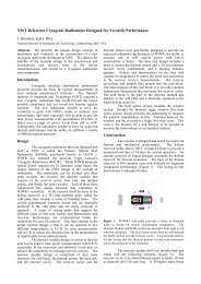
it is impossible to create fully transparent electrodes over a<br />
wide spectral range we avoided the problem by depositing<br />
a semitransparent electrode on a fraction (half) of the<br />
surface and thereby eliminated the IQD on this part. We<br />
thereby find the IQD on the uncoated surface. A picture of<br />
the detector is shown in fig.1.<br />
Figure 1. Picture of the Si detector. A semitransparent layer<br />
of gold is deposited on the left half of the surface. The<br />
Proceedings NEWRAD, 17-19 October 2005, Davos, Switzerland 63