ATSC 8-VSB demodulator and decoder
ATSC 8-VSB demodulator and decoder
ATSC 8-VSB demodulator and decoder

You also want an ePaper? Increase the reach of your titles
YUMPU automatically turns print PDFs into web optimized ePapers that Google loves.
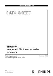
INTEGRATED CIRCUITS<br />
DATA SHEET<br />
TDA8960<br />
<strong>ATSC</strong> 8-<strong>VSB</strong> <strong>demodulator</strong> <strong>and</strong><br />
<strong>decoder</strong><br />
Preliminary specification<br />
File under Integrated Circuits, IC02<br />
1999 Jun 14
Philips Semiconductors<br />
Preliminary specification<br />
<strong>ATSC</strong> 8-<strong>VSB</strong> <strong>demodulator</strong> <strong>and</strong> <strong>decoder</strong><br />
TDA8960<br />
FEATURES<br />
General features<br />
• One-chip Advanced Television Systems Committee<br />
(<strong>ATSC</strong>)-compliant <strong>demodulator</strong> <strong>and</strong> concatenated trellis<br />
(Viterbi)/Reed Solomon <strong>decoder</strong> with de-interleaver <strong>and</strong><br />
de-r<strong>and</strong>omizer<br />
• 0.4 µm process<br />
• 3.3 V device<br />
• 64-lead QFP64 package<br />
• Boundary scan test<br />
• Output format: 8-bit wide bus.<br />
8-<strong>VSB</strong> <strong>demodulator</strong><br />
• On-chip digital circuitry for tuner Automatic Gain Control<br />
(AGC)<br />
• Square root raised cosine filter with 11.5% roll-off factor<br />
• Fully internal carrier recovery loop<br />
• Mostly internal clock recovery <strong>and</strong> AGC loops with<br />
programmable loop filters<br />
• External indication of <strong>demodulator</strong> lock.<br />
Adaptive equalizer<br />
• Feed forward including a Decision Feedback Equalizer<br />
(DFE) structure<br />
• Range of −2.3 to +10.5 µs<br />
• Adaptation based on <strong>ATSC</strong> field sync (trained) <strong>and</strong>/or<br />
8-<strong>VSB</strong> data (blind)<br />
• Trellis (Viterbi) <strong>decoder</strong><br />
• Rate 2 ⁄ 3 (Rate 1 ⁄ 2 Ungerboeck code based).<br />
I 2 C-bus interface<br />
• I 2 C-bus interface to initialize <strong>and</strong> monitor the<br />
<strong>demodulator</strong> <strong>and</strong> Forward Error Correction (FEC)<br />
<strong>decoder</strong>. Operation without I 2 C-bus control is possible<br />
(default).<br />
DOCUMENT REFERENCES<br />
See the <strong>ATSC</strong> URL on ‘http://www.atsc.com’ for the<br />
following related documents:<br />
• “<strong>ATSC</strong> Digital Television St<strong>and</strong>ard” (document no. A/53,<br />
issued 1995 Sep 16)<br />
• “Guide to the use of the <strong>ATSC</strong> Digital Television<br />
St<strong>and</strong>ard” (document no. A/54, issued 1995 Oct 04).<br />
APPLICATIONS<br />
• Digital <strong>ATSC</strong> compliant TV receivers<br />
• Personal computers with digital television capabilities<br />
• Set-top boxes.<br />
Reed Solomon <strong>decoder</strong><br />
• (207, 187 <strong>and</strong> T = 10) Reed Solomon code<br />
• Internal convolutional de-interleaving (I = 52; using<br />
internal memory)<br />
• External indication of uncorrectable error; transport error<br />
indicator bit in Motion Picture Export Group (MPEG)<br />
packet header is also set<br />
• Followed by de-r<strong>and</strong>omizer based on <strong>ATSC</strong> st<strong>and</strong>ard.<br />
ORDERING INFORMATION<br />
TYPE<br />
PACKAGE<br />
NUMBER NAME DESCRIPTION VERSION<br />
TDA8960 QFP64 plastic quad flat package; 64 leads (lead length 1.95 mm); body 14 × 20 × 2.8 mm SOT319-2<br />
1999 Jun 14 2
Philips Semiconductors<br />
Preliminary specification<br />
<strong>ATSC</strong> 8-<strong>VSB</strong> <strong>demodulator</strong> <strong>and</strong> <strong>decoder</strong><br />
TDA8960<br />
GENERAL DESCRIPTION<br />
The TDA8960 is an <strong>ATSC</strong>-compliant <strong>demodulator</strong> <strong>and</strong><br />
forward error correction <strong>decoder</strong> for reception of 8-<strong>VSB</strong><br />
modulated signals for terrestrial <strong>and</strong> cable applications:<br />
• Terrestrial: reception of 8-<strong>VSB</strong> modulated signals via<br />
st<strong>and</strong>ard 6 MHz VHF/UHF terrestrial TV channels<br />
(TV channels 2 to 69 in the United States)<br />
• Cable: reception of 8-<strong>VSB</strong> modulated signals via<br />
st<strong>and</strong>ard 6 MHz VHF/UHF cable TV channels.<br />
Most of the loop components needed to recover the data<br />
from the received symbols are internal. The only required<br />
external loop components are a low-speed serial D/A<br />
converter <strong>and</strong> a Voltage Controlled crystal Oscillator<br />
(VCXO) for the symbol timing recovery <strong>and</strong> an opamp<br />
integrator for the AGC. Loop parameters of the clock <strong>and</strong><br />
carrier recovery can be controlled by the I 2 C-bus.<br />
A tuner converts the incoming RF frequency to a fixed IF<br />
frequency centred at 44 MHz. The output of the tuner is<br />
filtered, followed by a down conversion in an IF block to a<br />
low IF frequency centred at 1 ⁄ 2 the <strong>VSB</strong> symbol rate (or a<br />
frequency of approximately 5.38 MHz). The low IF signal is<br />
applied to the A/D converter.<br />
To use its full input span, the A/D converter is located<br />
within what is typically a fine AGC loop which includes a<br />
variable gain stage at the output of the IF block. However,<br />
it is also possible to apply the TDA8960 AGC control<br />
output directly to the tuner. The detector for the TDA8960<br />
AGC output is located after the A/D converter <strong>and</strong><br />
determines the peak level of the incoming signals. After<br />
gain control, the low IF signal is sampled at a nominal rate<br />
of twice the <strong>VSB</strong> symbol frequency, or approximately<br />
21.5 MHz.<br />
The carrier recovery is performed completely internally.<br />
This function consists of a digital frequency <strong>and</strong> Frequency<br />
Phase-Locked Loop (FPLL).<br />
Data shaping is performed with a square root raised cosine<br />
(half Nyquist) filter with roll-off factor of 11.5%.<br />
Symbol timing recovery is performed mostly within the<br />
TDA8960, except that a low cost D/A converter <strong>and</strong> VCXO<br />
are required externally to generate the nominal 21.52 MHz<br />
clock signal for the A/D converter <strong>and</strong> TDA8960.<br />
After carrier recovery, half Nyquist filtering <strong>and</strong> symbol<br />
timing recovery, adaptive equalization is performed based<br />
on the use of the <strong>ATSC</strong> field sync (trained equalization)<br />
<strong>and</strong>/or the 8-<strong>VSB</strong> data itself (blind equalization).<br />
The adaptive equalizer uses a DFE structure.<br />
After trellis decoding, the stream is de-interleaved with a<br />
convolutional de-interleaver (interleaving depth 52).<br />
The memory for de-interleaving is on-chip. The Reed<br />
Solomon <strong>decoder</strong> is <strong>ATSC</strong>-compliant with a length of 207<br />
<strong>and</strong> can correct up to 10 bytes. The decoded stream is<br />
de-r<strong>and</strong>omized using a Pseudo R<strong>and</strong>om Bit Sequence<br />
(PRBS). Finally the data is passed to a First-In, First-Out<br />
(FIFO) register that prevents the appearance of irregular<br />
gaps in the output data.<br />
The output of the TDA8960 is an <strong>ATSC</strong>-compliant MPEG-2<br />
packet stream together with a clock. Furthermore some<br />
signal flags are provided to indicate the sync bytes <strong>and</strong> the<br />
valid data bytes. Uncorrected blocks are also indicated.<br />
The 8-bit wide MPEG-2 stream can be applied to an<br />
MPEG-2 transport demultiplexer.<br />
1999 Jun 14 3
Philips Semiconductors<br />
Preliminary specification<br />
<strong>ATSC</strong> 8-<strong>VSB</strong> <strong>demodulator</strong> <strong>and</strong> <strong>decoder</strong><br />
TDA8960<br />
QUICK REFERENCE DATA<br />
SYMBOL PARAMETER CONDITIONS MIN. TYP. MAX. UNIT<br />
V DDD digital supply voltage 3.0 3.3 3.6 V<br />
I DDD(tot) total digital supply current V DDD = 3.3 V − 300 − mA<br />
f clk clock frequency − 21.52 − MHz<br />
f sym symbol frequency − 10.76 − Msymbols/s<br />
IL implementation loss − − − dB<br />
α ro half Nyquist filter roll-off factor − 11.5 − %<br />
t acq acquisition time note 1 − − 290 ms<br />
T amb ambient temperature −20 − +70 °C<br />
P tot total power dissipation − 1.0 − W<br />
Note<br />
1. This corresponds to 12 training sequences.<br />
1999 Jun 14 4
Philips Semiconductors<br />
Preliminary specification<br />
<strong>ATSC</strong> 8-<strong>VSB</strong> <strong>demodulator</strong> <strong>and</strong> <strong>decoder</strong><br />
TDA8960<br />
BLOCK DIAGRAM<br />
h<strong>and</strong>book, full pagewidth<br />
EQLOCKINDIC<br />
LOCKINDIC<br />
AGCOUT<br />
ADIN0 to ADIN9<br />
53<br />
54<br />
56 1 to 8, 11, 12<br />
RESET<br />
27<br />
RSTAN<br />
LOCK<br />
DETECTORS<br />
DIGITAL FRONT-END (1)<br />
SERIAL<br />
DAC<br />
INTERFACE<br />
61<br />
62<br />
63<br />
64<br />
TRSDO<br />
TRSTB<br />
TRCS<br />
TRLD<br />
TRELLIS DECODER<br />
TDA8960<br />
SYNCHRO-<br />
NIZATION<br />
DE-INTERLEAVER<br />
REED SOLOMON DECODER<br />
BOUNDARY<br />
SCAN TEST<br />
17<br />
21<br />
20<br />
18<br />
19<br />
TDI<br />
TDO<br />
TRST<br />
TMS<br />
TCK<br />
DE-RANDOMIZER<br />
FIFO<br />
I 2 C-BUS<br />
INTERFACE<br />
13<br />
16<br />
14<br />
15<br />
A0<br />
A1<br />
SCL<br />
SDA<br />
59<br />
29<br />
31 to 33<br />
35 to 37<br />
39, 40 22 24 25<br />
23, 34,<br />
45, 57,<br />
9, 26,<br />
41, 60<br />
30, 38,<br />
49,55,<br />
10, 28,<br />
42, 58<br />
CLK<br />
DATACLK<br />
ERROR<br />
SOP DATAVALID<br />
V SSD1 to V SSD8<br />
DATA7 to DATA0<br />
V DDD1 to V DDD8<br />
MGR598<br />
(1) The digital front-end consists of the following circuits:<br />
- Fine AGC<br />
- Carrier recovery<br />
- Half Nyquist filter<br />
- Symbol timing recovery<br />
- Sync recovery <strong>and</strong> pilot removal<br />
- Adaptive equalization.<br />
Fig.1 Block diagram.<br />
1999 Jun 14 5
Philips Semiconductors<br />
Preliminary specification<br />
<strong>ATSC</strong> 8-<strong>VSB</strong> <strong>demodulator</strong> <strong>and</strong> <strong>decoder</strong><br />
TDA8960<br />
PINNING<br />
SYMBOL PIN I/O DESCRIPTION<br />
ADIN0 1 I data input bit 0 from ADC<br />
ADIN1 2 I data input bit 1 from ADC<br />
ADIN2 3 I data input bit 2 from ADC<br />
ADIN3 4 I data input bit 3 from ADC<br />
ADIN4 5 I data input bit 4 from ADC<br />
ADIN5 6 I data input bit 5 from ADC<br />
ADIN6 7 I data input bit 6 from ADC<br />
ADIN7 8 I data input bit 7 from ADC<br />
V DDD5 9 − digital supply voltage 5 (3.3 V)<br />
V SSD5 10 − digital core ground 5<br />
ADIN8 11 I data input bit 8 from ADC<br />
ADIN9 12 I data input bit 9 from ADC<br />
A0 13 I I 2 C-bus slave address bit 0<br />
SCL 14 I I 2 C-bus clock<br />
SDA 15 I/O I 2 C-bus serial data<br />
A1 16 I I 2 C-bus slave address bit 1<br />
TDI 17 I TAP controller data input; note 1<br />
TMS 18 I TAP controller test mode select; note 1<br />
TCK 19 I TAP controller test clock; note 1<br />
TRST 20 I TAP controller asynchronous reset; note 1<br />
TDO 21 O TAP controller test data output (3-state); note 1<br />
ERROR 22 O transport packet block error signal<br />
V DDD1 23 − digital supply voltage 1 (3.3 V)<br />
SOP 24 O start of transport packet signal<br />
DATAVALID 25 O transport packet data valid signal<br />
V DDD6 26 − digital supply voltage 6 (3.3 V)<br />
RSTAN 27 I asynchronous reset<br />
V SSD6 28 − digital ground 6<br />
DATACLK 29 O transport interface data clock<br />
V SSD1 30 − digital ground 1<br />
DATA7 31 O transport packet data output bit 7<br />
DATA6 32 O transport packet data output bit 6<br />
DATA5 33 O transport packet data output bit 5<br />
V DDD2 34 − digital supply voltage 2 (3.3 V)<br />
DATA4 35 O transport packet data output bit 4<br />
DATA3 36 O transport packet data output bit 3<br />
DATA2 37 O transport packet data output bit 2<br />
V SSD2 38 − digital ground 2<br />
DATA1 39 O transport packet data output bit 1<br />
DATA0 40 O transport packet data output bit 0<br />
1999 Jun 14 6
Philips Semiconductors<br />
Preliminary specification<br />
<strong>ATSC</strong> 8-<strong>VSB</strong> <strong>demodulator</strong> <strong>and</strong> <strong>decoder</strong><br />
TDA8960<br />
SYMBOL PIN I/O DESCRIPTION<br />
V DDD7 41 − digital supply voltage 7 (3.3 V)<br />
V SSD7 42 − digital ground 7<br />
n.c. 43 not connected<br />
n.c. 44 not connected<br />
V DDD3 45 − digital supply voltage 3 (3.3 V)<br />
n.c. 46 not connected<br />
n.c. 47 not connected<br />
n.c. 48 not connected<br />
V SSD3 49 − digital ground 3<br />
n.c. 50 not connected<br />
n.c. 51 not connected<br />
n.c. 52 not connected<br />
LOCKINDIC 53 O lock indicator of front-end<br />
EQLOCKINDIC 54 O lock indicator of equalizer<br />
V SSD4 55 − digital ground 4<br />
AGCOUT 56 O AGC control signal (3-state)<br />
V DDD4 57 − digital supply voltage 4 (3.3 V)<br />
V SSD8 58 − digital ground 8<br />
CLK 59 I clock<br />
V DDD8 60 − digital supply voltage 8 (3.3 V)<br />
TRSDO 61 O serial data to DAC<br />
TRSTB 62 O strobe signal to DAC<br />
TRCS 63 O chip select signal to DAC<br />
TRLD 64 O load signal to DAC<br />
Note<br />
1. In accordance with the “IEEE 1149.1” st<strong>and</strong>ard; pads TCK, TDI, TMS <strong>and</strong> TRST are input pads with an internal<br />
pull-up transistor <strong>and</strong> pad TDO is a 3-state output pad.<br />
1999 Jun 14 7
Philips Semiconductors<br />
Preliminary specification<br />
<strong>ATSC</strong> 8-<strong>VSB</strong> <strong>demodulator</strong> <strong>and</strong> <strong>decoder</strong><br />
TDA8960<br />
h<strong>and</strong>book, full pagewidth<br />
TRLD<br />
TRCS<br />
TRSTB<br />
TRSDO<br />
V DDD8<br />
CLK<br />
V SSD8<br />
V DDD4<br />
AGCOUT<br />
V SSD4<br />
EQLOCKINDIC<br />
LOCKINDIC<br />
n.c.<br />
ADIN0<br />
1<br />
51<br />
n.c.<br />
ADIN1<br />
2<br />
50<br />
n.c.<br />
ADIN2<br />
3<br />
49<br />
V SSD3<br />
ADIN3<br />
4<br />
48<br />
n.c.<br />
ADIN4<br />
5<br />
47<br />
n.c.<br />
ADIN5<br />
6<br />
46<br />
n.c.<br />
ADIN6<br />
7<br />
45<br />
V DDD3<br />
ADIN7<br />
8<br />
44<br />
n.c.<br />
V DDD5<br />
9<br />
43<br />
n.c.<br />
V SSD5<br />
10<br />
TDA8960<br />
42<br />
V SSD7<br />
ADIN8<br />
11<br />
41<br />
V DDD7<br />
ADIN9<br />
12<br />
40<br />
DATA0<br />
A0<br />
13<br />
39<br />
DATA1<br />
SCL<br />
14<br />
38<br />
V SSD2<br />
SDA<br />
15<br />
37<br />
DATA2<br />
A1<br />
16<br />
36<br />
DATA3<br />
TDI<br />
17<br />
35<br />
DATA4<br />
TMS<br />
18<br />
34<br />
V DDD2<br />
TCK<br />
19<br />
33<br />
DATA5<br />
20<br />
21<br />
22<br />
23<br />
24<br />
25<br />
26<br />
27<br />
28<br />
29<br />
30<br />
TRST<br />
TDO<br />
ERROR<br />
31<br />
32<br />
64<br />
63<br />
62<br />
61<br />
60<br />
59<br />
58<br />
57<br />
56<br />
55<br />
54<br />
53<br />
52<br />
V DDD1<br />
SOP<br />
DATAVALID<br />
V DDD6<br />
RSTAN<br />
V SSD6<br />
DATACLK<br />
V SSD1<br />
DATA7<br />
DATA6<br />
MGR599<br />
Fig.2 Pin configuration.<br />
1999 Jun 14 8
Philips Semiconductors<br />
Preliminary specification<br />
<strong>ATSC</strong> 8-<strong>VSB</strong> <strong>demodulator</strong> <strong>and</strong> <strong>decoder</strong><br />
TDA8960<br />
FUNCTIONAL DESCRIPTION<br />
The internal architecture of the TDA8960 consists of<br />
basically two parts:<br />
• The front-end containing the AGC, carrier recovery, half<br />
Nyquist filter, symbol timing recovery, sync recovery <strong>and</strong><br />
adaptive equalization<br />
• The back-end containing the trellis <strong>decoder</strong>,<br />
de-interleaver, the Reed Solomon <strong>decoder</strong> <strong>and</strong><br />
de-r<strong>and</strong>omizer.<br />
AGC<br />
This block controls an analog gain over a range of up to<br />
±20 dB.<br />
The data from the A/D converter (Philips Semiconductors’<br />
TDA8763 is recommended) arrives at the <strong>VSB</strong><br />
<strong>demodulator</strong> via inputs ADIN9 to ADIN0, which is10-bit<br />
wide. The format of the incoming samples can be<br />
programmed using the I 2 C-bus accessible register 08H.<br />
By writing to bit 3 the format can be either twos<br />
complement or binary.<br />
The absolute value of the input signal is averaged over<br />
several samples. The filtered signal is compared to a<br />
threshold. The threshold consist of a 4-bit signed value<br />
which can be programmed using the I 2 C-bus. The 3-state<br />
output signal charges or discharges an off-chip ideal<br />
integrator <strong>and</strong> is used to control the gain controller of the<br />
tuner front-end module. The values of the signal are shown<br />
in Table 1.<br />
Table 1<br />
AGC output<br />
PIN AGCOUT<br />
COMMENT<br />
1 output of the filter is smaller than the<br />
threshold<br />
0 output of the filter is larger than the<br />
threshold<br />
Z output of the filter is equal to the<br />
threshold<br />
The analog low-pass filter or integrator circuit should be<br />
designed with an 8 ms time constant. The response of the<br />
gain amplifier is linear with respect to the control voltage<br />
over the desired range of operation.<br />
Carrier recovery<br />
This circuit recovers the frequency <strong>and</strong> phase of the pilot<br />
carrier. The spectrum during the carrier recovery is<br />
displayed in Fig.3.<br />
By default the carrier is present at 2.69 MHz. During carrier<br />
recovery a shift is applied such that the pilot is present at<br />
DC. It can happen that the pilot is present at the higher<br />
edge of the <strong>VSB</strong> spectrum. In this event the CR_INV bit in<br />
I 2 C-bus register 08H (see Table 13) can be set to make<br />
sure that after the shift the pilot is at DC.<br />
h<strong>and</strong>book, halfpage<br />
amplitude<br />
(dB)<br />
Fig.3 Signal spectrum during carrier recovery.<br />
The carrier recovery is capable of tracking a frequency<br />
offset of up to 100 kHz from the nominal frequency offset<br />
within 100 ms.<br />
By means of I 2 C-bus read register 03H the current<br />
frequency offset in the carrier recovery can be read.<br />
This value can be used for fine tuning applications.<br />
Sync recovery <strong>and</strong> pilot removal<br />
This block performs several functions including pilot<br />
removal, segment <strong>and</strong> field sync removal <strong>and</strong> rescale<br />
AGC based on the segment sync. If this block is able to<br />
find a data segment sync signal, the external pin<br />
LOCKINDIC is asserted. The value of this signal can also<br />
be read through I 2 C-bus control.<br />
Adaptive equalization<br />
5.38 MHz<br />
MGR600<br />
2.69 5.38 8.07<br />
frequency (MHz)<br />
The equalizer consists of a forward filter <strong>and</strong> a feedback<br />
filter section. Demodulated symbols from the<br />
synchronization <strong>and</strong> pilot removal block are received every<br />
symbol period. The equalizer tries to invert the effects of<br />
the channel on the transmitted symbol stream by filtering<br />
these symbols. The coefficients of the filters are updated<br />
every symbol period using the training sequence. There is<br />
also a provision to perform blind equalization. The filtered<br />
output is available for the next block, the trellis <strong>decoder</strong>.<br />
1999 Jun 14 9
Philips Semiconductors<br />
Preliminary specification<br />
<strong>ATSC</strong> 8-<strong>VSB</strong> <strong>demodulator</strong> <strong>and</strong> <strong>decoder</strong><br />
TDA8960<br />
The equalizer has been designed to correct a maximum<br />
pre-echo of 2.32 µs <strong>and</strong> a maximum post-echo of<br />
10.50 µs. The equalizer uses an overlapping DFE to<br />
reduce the effects of co-channel interference.<br />
The equalizer has been optimized to have a typical<br />
acquisition time of 12 training sequences, which<br />
corresponds to approximately 290 ms. The acquisition<br />
time has been defined as the time when the output<br />
signal-to-noise ratio reaches the Threshold Of Visibility<br />
(TOV). The <strong>ATSC</strong> defines a TOV of 14.9 dB for 8-<strong>VSB</strong>.<br />
Based on the training signal <strong>and</strong> the output of the equalizer<br />
the Mean Square Error (MSE) signal is generated. This<br />
16-bit value is used to control the channel adaptation<br />
process <strong>and</strong> is available though I 2 C-bus control.<br />
Control<br />
The TDA8960 contains a complicated finite state machine.<br />
This state machine controls the sequence of operations<br />
that must be performed when a valid <strong>VSB</strong> data signal is<br />
detected in order for it to be properly decoded into a<br />
stream of MPEG-2 transport packets. The following steps<br />
have to take place:<br />
1. The external tuner is directed to lock to a specified<br />
channel frequency. A <strong>VSB</strong> signal is present.<br />
2. The tuner AGC locks to an acceptable signal gain.<br />
3. The coarse AGC of the TDA8960 locks to acceptable<br />
A/D converter gain.<br />
4. The timing <strong>and</strong> carrier recovery loops lock to the<br />
symbol clock <strong>and</strong> the carrier frequency.<br />
5. The segment sync pattern is detected. The segment<br />
sync lock is acquired.<br />
6. The fine AGC locks.<br />
7. The field sync pattern is detected. The MSE of the<br />
received field sync training sequence is determined.<br />
8. The equalizer uses subsequent training sequences to<br />
adapt itself to the channel conditions.<br />
9. The equalizer adapts to the point that the MSE of the<br />
training sequence is sufficiently small. The trellis<br />
decoding, convolutional de-interleaving <strong>and</strong> Reed<br />
Solomon decoding processes all begin.<br />
10. Valid MPEG-2 transport packets are generated.<br />
The finite state machine consists of three states. After a<br />
reset has been applied, the state machine starts in state 0.<br />
STATE 0: CHANNEL ACQUISITION<br />
In this state either no channel signal is present or a<br />
channel signal is being acquired. The AGC, timing<br />
recovery <strong>and</strong> carrier recovery loops must first lock onto it.<br />
If the segment sync lock is lost, pin LOCKINDIC is LOW,<br />
or a hardware reset is applied to the <strong>VSB</strong> <strong>demodulator</strong>, the<br />
finite state machine returns to state 0.<br />
STATE 1: EQUALIZER TRAINING<br />
The finite state machine remains in state 1 until the MSE<br />
of the equalized training sequence falls below a certain<br />
threshold. It should be noted that in state 1 the back-end is<br />
continuously reset to make sure that after the <strong>demodulator</strong><br />
has locked onto a signal, the trellis <strong>decoder</strong> <strong>and</strong> following<br />
processing blocks begin at the start of the next complete<br />
data field. By means of I 2 C-bus registers 01H <strong>and</strong> 02H the<br />
MSE value of the equalizer can be read. This value can be<br />
used for applications such as antenna pointing.<br />
STATE 2: NORMAL OPERATION<br />
Normally the state machine would remain in state 2 as<br />
long as no synchronization error occurs. If the MSE of the<br />
equalized training sequence is exceeded for more than<br />
100 ms, the equalizer is reset for one symbol period <strong>and</strong><br />
the adaptation process starts again. If the <strong>demodulator</strong> is<br />
in this state, the EQLOCKINDIC pin signal goes up.<br />
The value of this signal can also be read through the<br />
I 2 C-bus.<br />
1999 Jun 14 10
Philips Semiconductors<br />
Preliminary specification<br />
<strong>ATSC</strong> 8-<strong>VSB</strong> <strong>demodulator</strong> <strong>and</strong> <strong>decoder</strong><br />
TDA8960<br />
DAC interface<br />
The TDA8960 D/A interface connects to an external off-chip serial D/A converter. It supports four different serial modes.<br />
EXTERNAL INTERFACE<br />
The DAC interface consists of pins 61 to 64; see Table 2.<br />
Table 2<br />
DAC interface<br />
PIN<br />
TRSDO<br />
TRSTB<br />
TRCS<br />
TRLD<br />
FUNCTION<br />
serial data output<br />
strobe signal which can be used by the DAC to shift in serial data<br />
chip select signal for DAC is also used by some DACs to load serially shifted data in the internal<br />
parallel register on the positive edge<br />
load signal used by some DACs to load serially shifted data in the internal parallel latches<br />
OUTPUT MODES<br />
Table 3 shows which DACs can be used in the different output modes.<br />
Table 3<br />
DAC serial interface modes <strong>and</strong> DAC types<br />
OUTPUT MODE POLARITY SET-UP TIME (ns) EXAMPLE DEVICE<br />
0 +dF/dV 67 Maxim<br />
MAX531, MAX538, MAX539, MAX504 <strong>and</strong> MAX515<br />
Texas Instruments TLC5615<br />
Sipex SP9500 <strong>and</strong> SP960<br />
Linear Technology TLC1451<br />
1 +dF/dV 45 Analog Devices AD7943<br />
2 +dF/dV 45 Analog Devices DAC8512<br />
3 −dF/dV 67 same types as mode 0<br />
The operating mode is programmed by means of the I 2 C-bus interface. Bits 4 <strong>and</strong> 5 of registers 09H control the mode;<br />
see Table 13.<br />
The timing diagrams of the different serial modes are shown in Fig.4. Modes 0 <strong>and</strong> 3 do not use the load signal available<br />
at pin TRLD. In mode 3 the output of the timing recovery low-pass filter is inverted to control VCXOs which have a<br />
negative dF/dV. Modes 0 <strong>and</strong> 3 can provide up to 67 ns of the serial data set-up time from the moment the TRSDO output<br />
has a new data bit until the start of the TRSTB pulse.<br />
In mode 1 the TRCS pin is not used.<br />
1999 Jun 14 11
Philips Semiconductors<br />
Preliminary specification<br />
<strong>ATSC</strong> 8-<strong>VSB</strong> <strong>demodulator</strong> <strong>and</strong> <strong>decoder</strong><br />
TDA8960<br />
h<strong>and</strong>book, full TRCS pagewidth<br />
TRSTB<br />
TRSDO D11 D10 D9 D8 D7 D6 D5 D4 D3 D2 D1 D0<br />
MGR601<br />
a. Modes 0 <strong>and</strong> 3<br />
h<strong>and</strong>book, full TRSTB pagewidth<br />
TRSDO D11 D10 D9 D8 D7 D6 D5 D4 D3 D2 D1 D0<br />
TRLD<br />
MGR602<br />
b. Mode 1<br />
h<strong>and</strong>book, full TRCS pagewidth<br />
TRSTB<br />
TRSDO D11 D10 D9 D8 D7 D6 D5 D4 D3 D2 D1 D0<br />
TRLD<br />
MGR603<br />
c. Mode 2<br />
Fig.4 Timing diagrams of the different DAC serial interface modes.<br />
1999 Jun 14 12
Philips Semiconductors<br />
Preliminary specification<br />
<strong>ATSC</strong> 8-<strong>VSB</strong> <strong>demodulator</strong> <strong>and</strong> <strong>decoder</strong><br />
TDA8960<br />
Transport stream interface<br />
The transport stream interface provides an output of 8-bit<br />
parallel MPEG-2 transport packets at a data rate of<br />
5.38 Mbytes/s.<br />
IMPLEMENTATION<br />
The transport interface consists of a FIFO, which has two<br />
tasks:<br />
1. Removal of the field sync segment from the generation<br />
of output data<br />
2. Increase of the data rate of the de-r<strong>and</strong>omizer from<br />
2.69 to 5.38 MHz.<br />
Basically the 208 bytes of a field segment (187 data bytes,<br />
20 error correcting bytes <strong>and</strong> one segment sync byte) are<br />
distributed over the remaining 312 data segments.<br />
The FIFO has a depth of two data segments. As the output<br />
data rate is 5.38 MHz we have to distribute 416 bytes, or<br />
two field sync data segments over 312 data segments.<br />
Every MPEG-2 transport packet corresponding to a data<br />
segment gets a delay equal to one 5.38 MHz clock cycle.<br />
Further, every third MPEG-2 transport packet gets an<br />
extra delay of one 5.38 MHz transport packet.<br />
EXTERNAL INTERFACE<br />
The transport stream consists of four signals <strong>and</strong> one data<br />
bus as shown in Table 4.<br />
Table 4<br />
Transport stream interface<br />
NAME<br />
DATACLK<br />
DATAVALID<br />
DATA[7 to 0]<br />
SOP<br />
ERROR<br />
FUNCTION<br />
output clock<br />
valid <strong>demodulator</strong> output data or one valid MPEG transport packet<br />
output data stream (8-bit wide output bus)<br />
indicates the start of a packet. It goes HIGH at the start of a packet <strong>and</strong> remains HIGH<br />
during the first byte of the packet, the so called sync byte<br />
a transport packet error indicator, which is HIGH for each 188 byte transport packet in<br />
which the Reed Solomon <strong>decoder</strong> found more errors than it could correct<br />
FUNCTIONAL DESCRIPTION<br />
The timing of the transport stream interface signals is shown in Fig.5.<br />
h<strong>and</strong>book, full pagewidth<br />
185.9 ns<br />
DATACLK<br />
77.5 µs<br />
DATAVALID<br />
188 bytes/34.9 µs<br />
DATA7 to DATA0<br />
MPEG-2<br />
00H<br />
sync byte<br />
00H sync<br />
185.9 ns<br />
SOP<br />
188 bytes/34.9 µs<br />
ERROR<br />
MGR604<br />
Fig.5 Timing diagram of the transport interface (normal mode).<br />
1999 Jun 14 13
Philips Semiconductors<br />
Preliminary specification<br />
<strong>ATSC</strong> 8-<strong>VSB</strong> <strong>demodulator</strong> <strong>and</strong> <strong>decoder</strong><br />
TDA8960<br />
The DATACLK signal is the 5.38 MHz <strong>demodulator</strong> output<br />
clock. It is derived from the system clock of 21.52 MHz.<br />
A few remarks can be made about the DATACLK signal:<br />
• If a reset is applied, DATACLK becomes LOW; it<br />
remains LOW until reset is released <strong>and</strong> the symbol<br />
timing recovery block has detected the synchronization<br />
signals<br />
• After a channel change the DATACLK signal stops; it<br />
starts again after the system has been locked on to a<br />
valid signal<br />
• If the Reed Solomon <strong>decoder</strong> produces an invalid<br />
transport packet <strong>and</strong> the ERROR signal is asserted the<br />
DATACLK signal continues to change state<br />
• If the sync recovery block is not able to detect the field<br />
sync or data segment sync, DATACLK will not change.<br />
The DATAVALID signal indicates valid <strong>demodulator</strong> output<br />
data or one valid MPEG-2 transport packet. It is active<br />
HIGH for 188 bytes, or 34.9 µs. The zero bytes to be sent<br />
after the 188 valid bytes of the transport packet can be<br />
considered to be zeroed parity bytes.<br />
SOP or start of packet signal is HIGH during the first byte<br />
of the packet.<br />
The ERROR signal indicates that the transport packet<br />
contains uncorrectable output. The ERROR signal<br />
becomes HIGH in the following situations:<br />
• If the Reed Solomon <strong>decoder</strong> is unable to correct all<br />
errors in a transport packet<br />
• After a reset has been applied, the ERROR signal is<br />
asserted; it remains HIGH until a valid transport packet<br />
is produced by the <strong>demodulator</strong><br />
• If the <strong>demodulator</strong> is out of sync, thus can not detect the<br />
field sync <strong>and</strong> segment sync in the incoming data<br />
stream.<br />
The ERROR signal can be asserted in the middle of a<br />
transport packet.<br />
Sync byte <strong>and</strong> transport error indicator<br />
The structure of a transport packet header is shown in<br />
Fig.6. For the <strong>VSB</strong> <strong>demodulator</strong> only the first two bytes of<br />
the so called transport packet header are important.<br />
The first byte in each header of a transport packet is the so<br />
called MPEG-2 packet synchronization byte (sync byte).<br />
As specified in the MPEG-2 st<strong>and</strong>ard, this sync byte must<br />
have the same value for all packets. The <strong>VSB</strong> <strong>demodulator</strong><br />
IC sets this byte for each outgoing transport packet to 47H.<br />
The MSB of the second byte in the transport packet is the<br />
transport_error_indicator bit. It indicates that the Reed<br />
Solomon <strong>decoder</strong> was not able to correct all errors <strong>and</strong> the<br />
transport packet has invalid data.<br />
h<strong>and</strong>book, full pagewidth<br />
188 bytes<br />
adaptation field<br />
(if present)<br />
payload<br />
(if present)<br />
0<br />
transport packet header<br />
1 0 0 0 1 1 1<br />
1st byte<br />
sync byte<br />
4th byte<br />
transport_error_indicator<br />
MSB<br />
LSB<br />
MGR605<br />
Fig.6 The structure of a transport packet header.<br />
1999 Jun 14 14
Philips Semiconductors<br />
Preliminary specification<br />
<strong>ATSC</strong> 8-<strong>VSB</strong> <strong>demodulator</strong> <strong>and</strong> <strong>decoder</strong><br />
TDA8960<br />
Boundary scan interface<br />
The TDA8960 Test Access Port (TAP) conforms to the<br />
“IEEE 1149.1 Joint Test Action Group (JTAG)” st<strong>and</strong>ard.<br />
It is used for board level testing of integrated circuits <strong>and</strong><br />
for testing the internals of an integrated circuit. The JTAG<br />
st<strong>and</strong>ard defines on-chip test logic, which consists of an<br />
instruction register, a group of test data registers including<br />
a bypass register <strong>and</strong> a boundary scan register, four<br />
dedicated pins collectively called the Test Access Port<br />
(TAP) <strong>and</strong> a TAP controller.<br />
INSTRUCTION REGISTER<br />
The instruction register consists of four bits without parity.<br />
There are five defined public instructions; see Table 5.<br />
Table 5<br />
Public instruction codes<br />
INSTRUCTION CODE SELECTED DATA REGISTER<br />
BYPASS (1) 1111 bypass (initialized state)<br />
SAMPLE (2) 0001 boundary scan<br />
EXTEST (3) 0000 boundary scan<br />
INTEST (4) 0011 boundary scan<br />
IDCODE (5) 0010 identification or bypass<br />
Notes<br />
1. The bypass instruction provides a minimum length (1-bit) serial path between the TDI <strong>and</strong> TDO pins when no test<br />
operation is required.<br />
2. This instruction can be used to take a sample of the inputs <strong>and</strong> outputs during normal operation of the component.<br />
It can also be used to preload data values into the latched outputs of the boundary scan register.<br />
3. This instructions allows testing off-chip circuitry <strong>and</strong> board level interconnections.<br />
4. This instruction allows low speed, static testing of the on-chip logic. It can also be used after the chip is mounted on<br />
a printed circuit board.<br />
5. This instruction will return the manufacturer ID, part number code <strong>and</strong> version code. For the TDA8960 the<br />
manufacturer ID is ‘B00000010101’, the part number code is ‘S<strong>VSB</strong>’ <strong>and</strong> the version code is ‘D1’.<br />
In addition three private instructions are implemented to control different test modes; see Table 6.<br />
Table 6<br />
Private instruction codes<br />
INSTRUCTION CODE TEST MODE<br />
SCAN_TEST 1000 test on-chip scan chains<br />
BIST_TEST 1001 BIST test of de-interleaver RAM<br />
RAM_TEST 1010 scan test of the on-chip memories<br />
CHAR_MODE 1011 characterization mode<br />
In the characterization mode the IC is scan-testable in the<br />
same way as in the scan test mode. However the outputs<br />
are not switched to the scan chain outputs. The outputs<br />
retain their functionality. It is now possible to scan test<br />
pattern through the logic <strong>and</strong> to verify if the timing<br />
constrains at the outputs are met.<br />
EXTERNAL INTERFACE<br />
The TAP consists of five pins as shown in Table 7.<br />
1999 Jun 14 15
Philips Semiconductors<br />
Preliminary specification<br />
<strong>ATSC</strong> 8-<strong>VSB</strong> <strong>demodulator</strong> <strong>and</strong> <strong>decoder</strong><br />
TDA8960<br />
Table 7<br />
TAP external interface<br />
SIGNAL TYPE DESCRIPTION<br />
TMS I test mode select<br />
TCK I test clock<br />
TDI I test data input<br />
TDO O test data output<br />
TRST I test asynchronous reset<br />
OPERATION<br />
The TAP controller is a finite state machine. It selects a<br />
JTAG instruction or a data register to store the input based<br />
on the TMS signal, receives instructions <strong>and</strong> data on the<br />
TDI pin, executes the instruction when triggered by TMS,<br />
<strong>and</strong> shifts data out of TDO.<br />
h<strong>and</strong>book, halfpage<br />
I 2 C-BUS<br />
MASTER<br />
TDA8960<br />
R pu<br />
V DD<br />
R pu<br />
TCK provides the clock signal for the test logic required by<br />
the st<strong>and</strong>ard. TCK is asynchronous to the system clock.<br />
Stored devices in the JTAG controller must retain their<br />
state indefinitely when TCK is stopped at logic 0.<br />
SCL<br />
SDA<br />
MGR606<br />
The signal received at TMS is decoded by the TAP<br />
controller to control test functions. The logic is required to<br />
sample TMS at the rising edge of TCK.<br />
Serial test instructions <strong>and</strong> test data are received at TDI.<br />
The TDI signal is required to be sampled at the rising edge<br />
of TCK. When test data is shifted from TDI to TDO, the<br />
data must appear without inversion at TDO after a number<br />
of rising <strong>and</strong> falling edges of TCK, determined by the<br />
length of the instruction or test data register selected.<br />
TDO is the serial output for test instructions <strong>and</strong> data from<br />
the TAP controller. Changes in the state of TDO must<br />
occur after the falling edge of TCK. This is because<br />
devices connected to TDO are required to sample TDO at<br />
the rising edge of TCK. The TDO driver must be in an<br />
inactive state (i.e. TDO line must be flat) except when the<br />
scanning of data is in progress.<br />
I 2 C-bus interface<br />
The I 2 C-bus interface is used to write control information to<br />
<strong>and</strong> read low-speed diagnostic information from the<br />
TDA8960. The key features of the I 2 C-bus interface are:<br />
• I 2 C-bus data rate up to 400 kbits/s<br />
• Support for only 7-bit addressing <strong>and</strong> the possibility of<br />
modifying the slave address externally.<br />
A typical system using the I 2 C-bus interface is illustrated in<br />
Fig.7. The TDA8960 is connected as a slave to a master<br />
through SCL <strong>and</strong> SDA. Note that the bus has one pull-up<br />
resistor for each of the clock <strong>and</strong> data lines.<br />
EXTERNAL INTERFACE<br />
The I 2 C-bus interface consists of four signals as shown in<br />
Table 8.<br />
Table 8<br />
Fig.7 Typical I 2 C-bus system implementation.<br />
I 2 C-bus external interface<br />
SIGNAL TYPE DESCRIPTION<br />
SDA I/O I 2 C-bus serial data<br />
SCL I I 2 C-bus clock<br />
A0 I I 2 C-bus slave address bit 0<br />
A1 I I 2 C-bus slave address bit 1<br />
The TDA8960 has 3.3 V I/O <strong>and</strong> I 2 C-bus pins. Therefore,<br />
in a complete system some circuitry might be necessary to<br />
allow ICs with different supply voltages to communicate<br />
<strong>and</strong> be controlled. This has been described in an<br />
application report available from Philips Semiconductors<br />
(application report “AN97055”, issued 1997 Aug 04).<br />
1999 Jun 14 16
Philips Semiconductors<br />
Preliminary specification<br />
<strong>ATSC</strong> 8-<strong>VSB</strong> <strong>demodulator</strong> <strong>and</strong> <strong>decoder</strong><br />
TDA8960<br />
ADDRESSING THE DEVICE<br />
Addressing the <strong>VSB</strong> <strong>demodulator</strong> over the system the<br />
I 2 C-bus requires that the 7-bit slave address (A6 to A0) of<br />
the device is sent over the bus in accordance with the<br />
protocols, together with the R/W bit equal to logic 1 or 0 to<br />
write or read data respectively.<br />
The slave address of the device is shown in Table 9. Bits<br />
0 to 6 are predefined, but bits 0 <strong>and</strong> 1 can be set using the<br />
external pins A0 <strong>and</strong> A1.<br />
Table 9<br />
Slave address<br />
A6 A5 A4 A3 A2 A1 A0 R/W<br />
0 0 0 1 1 A1 A0 0 = write<br />
1 = read<br />
h<strong>and</strong>book, full pagewidth<br />
(1)(2) (1) (1)(3) (4)(5) (1) (4)(5) (1) (4)(5)(6) (1)(7)<br />
S SLAVE ADDRESS R/W A DATA A DATA A/A P<br />
(8)<br />
MGR607<br />
(1) From master to slave<br />
(2) S = START condition<br />
(3) Logic 0 (write)<br />
(4) From slave to master<br />
(5) A = acknowledge (SDA LOW)<br />
(6) A = not acknowledge (SDA HIGH)<br />
(7) P = STOP condition<br />
(8) Data transferred (n bytes + acknowledge).<br />
Fig.8 A master-transmitter addresses a slave receiver with a 7-bit address (write access).<br />
A write operation is shown in Fig.8. After the START<br />
condition, the slave address followed by the R/W bit is<br />
transmitted. The receiver, the TDA8960, sends an<br />
acknowledge <strong>and</strong> the transmitter starts sending the<br />
register values. After each received byte, the TDA8960<br />
sends an acknowledge. The transfer stops if the TDA8960<br />
does not acknowledge the transfer <strong>and</strong>/or the master<br />
sends a STOP condition.<br />
If register 08H has to be written to, eight consecutive bytes<br />
are written. The first corresponds to register 01H, the<br />
second to 02H <strong>and</strong> so on. The TDA8960 will<br />
auto-increment the accessed address automatically. Up to<br />
ten consecutive addresses can be written.<br />
In Table 11 the default values are given for a number of<br />
reserved addresses <strong>and</strong> reserved bits of certain<br />
addresses. These correct default values have to be written<br />
in order to prevent unexpected behaviour of the IC.<br />
Figure 9 shows a read operation. The master sends a<br />
START condition followed by the slave address <strong>and</strong> the<br />
R/W bit is set to logic 1. The slave returns an acknowledge<br />
followed by the value of the first address. The master<br />
sends another acknowledge <strong>and</strong> the next value of the<br />
address is returned. If the master transmits a STOP<br />
condition after the acknowledge, the transfer is stopped.<br />
Up to three consecutive addressed (00H to 03H) can be<br />
read.<br />
1999 Jun 14 17
Philips Semiconductors<br />
Preliminary specification<br />
<strong>ATSC</strong> 8-<strong>VSB</strong> <strong>demodulator</strong> <strong>and</strong> <strong>decoder</strong><br />
TDA8960<br />
h<strong>and</strong>book, full pagewidth<br />
(1)(2) (1) (1)(3) (4)(5) (4) (1)(5) (4) (1)(6) (1)(7)<br />
S SLAVE ADDRESS R/W A DATA A DATA A P<br />
(8)<br />
MGR608<br />
(1) From master to slave.<br />
(2) S = START condition.<br />
(3) Logic 1 (read).<br />
(4) From slave to master.<br />
(5) A = acknowledge (SDA LOW).<br />
(6) A = not acknowledge (SDA HIGH).<br />
(7) P = STOP condition.<br />
(8) Data transferred (n bytes + acknowledge).<br />
Fig.9 A master-transmitter addresses a slave receiver with a 7-bit address (read access).<br />
Table 10 I 2 C-bus control register overview (write); note 1<br />
FUNCTION ADDRESS D7 D6 D5 D4 D3 D2 D1 D0<br />
Operation 00H GNRL_RST INITIAL_RST<br />
Reserved<br />
01H<br />
Reserved<br />
02H<br />
Operation 03H AGC_THRES<br />
Reserved<br />
04H<br />
Reserved<br />
05H<br />
Reserved<br />
06H<br />
Reserved<br />
07H<br />
Carrier recovery 08H AD_FMT CR_INV<br />
Timing recovery 09H INTMOD<br />
Note<br />
1. Do not write past address 09H.<br />
Table 11 I 2 C-bus control registers (default settings after reset)<br />
FUNCTION ADDRESS D7 D6 D5 D4 D3 D2 D1 D0<br />
Operation 00H 0 0 0 0 0 0 0 0<br />
Reserved 01H 0 0 0 0 0 0 0 0<br />
Reserved 02H 0 0 0 0 0 1 0 0<br />
Operation 03H 0 0 0 0 0 0 0 0<br />
Reserved 04H 0 0 0 0 0 0 1 0<br />
Reserved 05H 1 0 0 0 0 0 0 0<br />
Reserved 06H 0 0 0 0 0 0 0 0<br />
Reserved 07H 1 1 0 0 1 0 1 0<br />
Carrier recovery 08H 0 0 0 0 0 1 0 0<br />
Timing recovery 09H 0 0 0 0 0 0 0 0<br />
1999 Jun 14 18
Philips Semiconductors<br />
Preliminary specification<br />
<strong>ATSC</strong> 8-<strong>VSB</strong> <strong>demodulator</strong> <strong>and</strong> <strong>decoder</strong><br />
TDA8960<br />
Table 12 I 2 C-bus diagnostic registers overview (read); note 1<br />
FUNCTION ADDRESS D7 D6 D5 D4 D3 D2 D1 D0<br />
Operation 00H LOCK_INDICATOR EQ_LOCK_INDICATOR<br />
Equalizer 01H MSE[15 to 8]<br />
02H MSE[7 to 0]<br />
Carrier<br />
recovery<br />
03H CR_OFFSET[7 to 0]<br />
Note<br />
1. Do not read past address 03H.<br />
Table 13 I 2 C-bus control registers (write); notes 1 <strong>and</strong> 2<br />
ADDRESS FUNCTION COMMENTS BIT FIELD NAME VALUE<br />
00H operation reserved 7 to 2<br />
general reset 1 GNRL_RESET 0 = disable<br />
(note 1)<br />
1 = enable<br />
initial reset 0 INITIAL_RESET 0 = disable<br />
(note 2)<br />
1 = enable<br />
03H operation reserved 7 to 4<br />
AGC threshold 3 to 0 AGC_THRES<br />
value<br />
08H carrier reserved 7 to 4<br />
recovery A/D input 3 AD_FMT 0 = twos complement<br />
format<br />
1 = binary<br />
inverted 2 CR_INV 0 = pilot at 8.07 MHz<br />
spectrum<br />
1 = pilot at 2.69 MHz<br />
reserved 1 to 0<br />
09H<br />
timing<br />
recovery<br />
reserved 7 to 6<br />
DAC interface<br />
mode<br />
5 to 4 INT_MOD 00 = mode 0 (TRLD not used)<br />
01 = mode 1 (TRCS not used)<br />
10 = mode 2 (TRCS <strong>and</strong> TRLD are used)<br />
11 = mode 3 (TRLD not used; negative dF/dV<br />
reserved 3 to 0<br />
Notes<br />
1. Operating modes <strong>and</strong> control parameters are reset to their initial values.<br />
2. Operating modes <strong>and</strong> control parameters are not affected.<br />
1999 Jun 14 19
Philips Semiconductors<br />
Preliminary specification<br />
<strong>ATSC</strong> 8-<strong>VSB</strong> <strong>demodulator</strong> <strong>and</strong> <strong>decoder</strong><br />
TDA8960<br />
Table 14 I 2 C-bus diagnostic registers (read)<br />
ADDRESS FUNCTION COMMENTS BIT FIELD NAME<br />
00H operation reserved 7 to 3<br />
sync recovery lock indicator 2 LOCK_INDICATOR<br />
equalizer lock indicator 1 EQ_LOCK_INDICATOR<br />
reserved 0<br />
01H equalizer equalizer mean square error value 15 to 8 MSE<br />
02H 7 to 0 MSE<br />
03H carrier recovery carrier recovery offset 7 to 0 CR_OFFSET<br />
LIMITING VALUES<br />
In accordance with the Absolute Maximum Rating System (IEC 134).<br />
SYMBOL PARAMETER CONDITIONS MIN. TYP. MAX. UNIT<br />
V DDD digital supply voltage 3.0 3.3 3.6 V<br />
V I input voltage on any pin with respect<br />
−0.5 − V DDD + 0.5 V<br />
to digital ground (V SSD )<br />
I I DC current into any input − − tbf mA<br />
I O DC current out of any output − − tbf mA<br />
T j junction temperature 0 − 105 °C<br />
T stg storage temperature − − − °C<br />
T amb ambient temperature −20 +25 +70 °C<br />
P tot total power dissipation − 1.0 − W<br />
V es electrostatic h<strong>and</strong>ling note 1 −3000 − +3000 V<br />
note 2 −300 − +300 V<br />
Notes<br />
1. Human body model: C = 100 pF; R = 1.5 kΩ; 3 zaps positive <strong>and</strong> 3 zaps negative.<br />
2. Machine model: C = 200 pF; L = 0.5 µH; R = 10 Ω; 3 zaps positive <strong>and</strong> 3 zaps negative.<br />
THERMAL CHARACTERISTICS<br />
SYMBOL PARAMETER CONDITIONS VALUE UNIT<br />
R th(j-a) thermal resistance from junction to ambient in free air 55 K/W<br />
1999 Jun 14 20
Philips Semiconductors<br />
Preliminary specification<br />
<strong>ATSC</strong> 8-<strong>VSB</strong> <strong>demodulator</strong> <strong>and</strong> <strong>decoder</strong><br />
TDA8960<br />
DC CHARACTERISTICS<br />
V DDD = 3.3 V; V SSD = 0 V; T amb =25°C; unless otherwise specified; note 1.<br />
SYMBOL PARAMETER CONDITIONS MIN. TYP. MAX. UNIT<br />
Supply<br />
V DDD digital supply voltage 3.0 3.3 3.6 V<br />
I DDD digital supply current − 300 − mA<br />
Inputs<br />
V IL LOW-level input voltage − − 0.8 V<br />
V IH HIGH-level input voltage 2.0 − − V<br />
I LI input leakage current − − 1 µA<br />
C i input capacitance 8 − 25 pF<br />
Output<br />
V OL LOW-level output voltage − − 0.4 V<br />
V OH HIGH-level output voltage 2.4 − − V<br />
I OL LOW-level output current − − 4 mA<br />
3-state output, pin AGCOUT<br />
I O(Z) high-impedance output current − − 1 µA<br />
C O(Z) high-impedance output<br />
capacitance<br />
− − 100 pF<br />
I 2 C-bus, pins SDA <strong>and</strong> SCL<br />
V IL LOW-level input voltage −0.5 − 0.3V DDD V<br />
V IH HIGH-level input voltage 0.7V DDD − V DDD + 0.5 V<br />
V OL LOW-level output voltage 0 − 0.4 V<br />
V OH HIGH-level output voltage note 2 − − 3.3 V<br />
I OL LOW-level output current V OL = 0.4 V 3 − − mA<br />
I L leakage current V I =V SSD or V DDD − − ±10 µA<br />
C i input capacitance V I =V SSD − − 8 pF<br />
Notes<br />
1. All supply connections must be made to the same external power supply unit.<br />
2. Open-drain output, determined by V DDD via an external pull-up resistor.<br />
1999 Jun 14 21
Philips Semiconductors<br />
Preliminary specification<br />
<strong>ATSC</strong> 8-<strong>VSB</strong> <strong>demodulator</strong> <strong>and</strong> <strong>decoder</strong><br />
TDA8960<br />
AC CHARACTERISTICS<br />
V DDD = 3.3 V; V SSD = 0 V; T amb =25°C; unless otherwise specified.<br />
SYMBOL PARAMETER CONDITIONS MIN. TYP. MAX. UNIT<br />
System clock (pin CLK)<br />
f clk(sys) system clock frequency − 21.52 − MHz<br />
t CLKH system clock HIGH time − 21.23 − ns<br />
t CLKL system clock LOW time note 1 − 21.23 − ns<br />
A/D interface (pins ADIN[9 to 0])<br />
t su(A/D) A/D interface set-up time 5 − − ns<br />
t h(A/D) A/D interface hold time 5 − − ns<br />
DAC interface (pins TRSDO, TRCS, TRLD <strong>and</strong> TRSTB); see Fig.13<br />
t su(D/A) D/A interface set-up time − 40 − ns<br />
t h(D/A) D/A interface hold time − 0 − ns<br />
Transport stream interface (pins DATA[7 to 0], SOP, ERROR <strong>and</strong> DATAVALID); see Fig.14<br />
t su(D) transport interface data set-up time 5 − − ns<br />
t h(D) transport interface data hold time 5 − − ns<br />
t DATACLKL transport interface DATACLK LOW<br />
180 − − ns<br />
time<br />
t DATACLKH transport interface DATACLK HIGH<br />
180 − − ns<br />
time<br />
t DATCLKW transport interface DATACLK period 371.7 − − ns<br />
t DAT-VAL transport interface DATA to<br />
DATAVALID, ERROR <strong>and</strong> SOP<br />
0 − − ns<br />
I 2 C-bus (pins SDA <strong>and</strong> SCL); see Fig.10<br />
f SCL SCL clock frequency 0 − 400 kHz<br />
t BUF bus free time between a STOP <strong>and</strong><br />
1.3 − − µs<br />
START condition<br />
t HD;STA hold time (repeated) START<br />
condition; after this period the first<br />
clock pulse is generated<br />
0.6 − − µs<br />
t LOW LOW period of the SCL clock 1.3 − − µs<br />
t HIGH HIGH period of the SCL clock 0.6 − − µs<br />
t SU;STA set-up time for a repeated START<br />
0.6 − − µs<br />
condition<br />
t SU;STO set-up time for STOP condition 0.6 − − µs<br />
t HD;DAT data hold time 0 − 0.9 µs<br />
t SU;DAT data set-up time 100 − − ns<br />
t SP pulse width of spikes which must be<br />
tbf − tbf ns<br />
suppressed by the input filter<br />
t r rise time of both SDA <strong>and</strong> SCL<br />
signals<br />
note 2 20 + 0.1C b − 300 ns<br />
1999 Jun 14 22
Philips Semiconductors<br />
Preliminary specification<br />
<strong>ATSC</strong> 8-<strong>VSB</strong> <strong>demodulator</strong> <strong>and</strong> <strong>decoder</strong><br />
TDA8960<br />
SYMBOL PARAMETER CONDITIONS MIN. TYP. MAX. UNIT<br />
t f fall time of both SDA <strong>and</strong> SCL note 1 20 + 0.1C b − 300 ns<br />
signals<br />
C b capacitive load for each bus line − − 400 pF<br />
JTAG interface (pins TDO, TDI, TCK, TMS <strong>and</strong> TRST); see Fig.11<br />
t d(TCK-TDO) pin TCK to TDO valid delay 2 − 10 ns<br />
t su(i)(TCK) input set-up time to TCK 10 − − ns<br />
t h(i)(TCK) input hold time from TCK 2 − − ns<br />
Reset (pin RSTAN)<br />
t su(PO)L power-on set-up time LOW 23 − − ns<br />
Notes<br />
1. The chip clock (CLK) comes from a VXCO controlled by the external DAC. The control loop keeps the clock signal<br />
constant at a frequency twice the symbol rate.<br />
2. C b = total capacitance of one bus line in pF.<br />
1999 Jun 14 23
This text is here in white to force l<strong>and</strong>scape pages to be rotated correctly when browsing through the pdf in the Acrobat reader.This text is here in<br />
_white to force l<strong>and</strong>scape pages to be rotated correctly when browsing through the pdf in the Acrobat reader.This text is here inThis text is here in<br />
white to force l<strong>and</strong>scape pages to be rotated correctly when browsing through the pdf in the Acrobat reader. white to force l<strong>and</strong>scape pages to be ...<br />
1999 Jun 14 24<br />
SDA<br />
SCL<br />
t BUF<br />
t LOW t r<br />
t f<br />
t HD;STA<br />
t SP<br />
t HD;STA<br />
t SU;STO<br />
t<br />
P S<br />
t HD;DAT t HIGH t SU;DAT SU;STA<br />
Sr P<br />
MBC611<br />
h<strong>and</strong>book, full pagewidth<br />
Fig.10 I 2 C-bus timing diagram.<br />
<strong>ATSC</strong> 8-<strong>VSB</strong> <strong>demodulator</strong> <strong>and</strong> <strong>decoder</strong> TDA8960<br />
Philips Semiconductors Preliminary specification
Philips Semiconductors<br />
Preliminary specification<br />
<strong>ATSC</strong> 8-<strong>VSB</strong> <strong>demodulator</strong> <strong>and</strong> <strong>decoder</strong><br />
TDA8960<br />
h<strong>and</strong>book, full pagewidth<br />
TCK<br />
t d(TCK-TDO)<br />
t su(i)(TCK)<br />
t h(i)(TCK)<br />
TDO<br />
valid<br />
MGR609<br />
Fig.11 JTAG I/O timing.<br />
h<strong>and</strong>book, full pagewidth<br />
T cy(CLK)<br />
t su(ADIN)<br />
CLK<br />
t h(ADIN)<br />
ADIN9 to ADIN0<br />
valid<br />
MGR610<br />
T cy(clk) = 46.47 ns.<br />
Fig.12 Input timing.<br />
h<strong>and</strong>book, full pagewidth<br />
TRSTB<br />
t su(D/A)<br />
t h(D/A)<br />
TRSDO<br />
valid<br />
MGR611<br />
Fig.13 Serial D/A converter interface I/O timing.<br />
1999 Jun 14 25
Philips Semiconductors<br />
Preliminary specification<br />
<strong>ATSC</strong> 8-<strong>VSB</strong> <strong>demodulator</strong> <strong>and</strong> <strong>decoder</strong><br />
TDA8960<br />
h<strong>and</strong>book, full pagewidth<br />
t DATCLKW<br />
t DATACLKH<br />
t DATACLKL<br />
DATACLK<br />
DATA7 to DATA0<br />
t su(D)<br />
t DAT-VAL<br />
t h(D)<br />
valid<br />
ERROR<br />
VALID<br />
SOP<br />
valid<br />
MGR612<br />
Fig.14 Transport interface timing.<br />
1999 Jun 14 26
Philips Semiconductors<br />
Preliminary specification<br />
<strong>ATSC</strong> 8-<strong>VSB</strong> <strong>demodulator</strong> <strong>and</strong> <strong>decoder</strong><br />
TDA8960<br />
APPLICATION INFORMATION<br />
h<strong>and</strong>book, full pagewidth<br />
AGC<br />
terrestial/cable<br />
UHF/VHF<br />
TUNER<br />
LOW<br />
IF<br />
A/D<br />
CONVERTER<br />
TDA8960<br />
MPEG<br />
transport stream<br />
21.52 MHz<br />
VCXO<br />
D/A<br />
CONVERTER<br />
I 2 C-BUS<br />
CONTROLLER<br />
I 2 C-bus<br />
MGR597<br />
Fig.15 Front-end unit for reception of 8-<strong>VSB</strong> signals.<br />
1999 Jun 14 27
Philips Semiconductors<br />
Preliminary specification<br />
<strong>ATSC</strong> 8-<strong>VSB</strong> <strong>demodulator</strong> <strong>and</strong> <strong>decoder</strong><br />
TDA8960<br />
PACKAGE OUTLINE<br />
QFP64: plastic quad flat package; 64 leads (lead length 1.95 mm); body 14 x 20 x 2.8 mm<br />
SOT319-2<br />
c<br />
y<br />
X<br />
51 33<br />
52<br />
32<br />
A<br />
Z E<br />
e<br />
E<br />
H E<br />
A<br />
A 2<br />
A 1<br />
(A ) 3<br />
pin 1 index<br />
w M<br />
L p<br />
θ<br />
L<br />
64<br />
1<br />
19<br />
20<br />
detail X<br />
e<br />
b p<br />
w M<br />
Z D<br />
b p<br />
v M B<br />
v M<br />
A<br />
D<br />
HD<br />
B<br />
0 5 10 mm<br />
scale<br />
DIMENSIONS (mm are the original dimensions)<br />
A<br />
UNIT<br />
max.<br />
A 1 A 2 A 3 b p c D (1) E (1) e H H E L L p v w y (1) Z (1)<br />
D<br />
ZD<br />
E<br />
mm<br />
3.20<br />
0.25<br />
0.05<br />
2.90<br />
2.65<br />
0.25<br />
0.50<br />
0.35<br />
0.25<br />
0.14<br />
20.1<br />
19.9<br />
14.1<br />
13.9<br />
1<br />
24.2<br />
23.6<br />
18.2<br />
17.6<br />
1.95<br />
1.0<br />
0.6<br />
0.2<br />
0.2 0.1<br />
1.2<br />
0.8<br />
1.2<br />
0.8<br />
θ<br />
o<br />
7<br />
o<br />
0<br />
Note<br />
1. Plastic or metal protrusions of 0.25 mm maximum per side are not included.<br />
OUTLINE<br />
VERSION<br />
REFERENCES<br />
IEC JEDEC EIAJ<br />
EUROPEAN<br />
PROJECTION<br />
ISSUE DATE<br />
SOT319-2<br />
95-02-04<br />
97-08-01<br />
1999 Jun 14 28
Philips Semiconductors<br />
Preliminary specification<br />
<strong>ATSC</strong> 8-<strong>VSB</strong> <strong>demodulator</strong> <strong>and</strong> <strong>decoder</strong><br />
TDA8960<br />
SOLDERING<br />
Introduction to soldering surface mount packages<br />
This text gives a very brief insight to a complex technology.<br />
A more in-depth account of soldering ICs can be found in<br />
our “Data H<strong>and</strong>book IC26; Integrated Circuit Packages”<br />
(document order number 9398 652 90011).<br />
There is no soldering method that is ideal for all surface<br />
mount IC packages. Wave soldering is not always suitable<br />
for surface mount ICs, or for printed-circuit boards with<br />
high population densities. In these situations reflow<br />
soldering is often used.<br />
Reflow soldering<br />
Reflow soldering requires solder paste (a suspension of<br />
fine solder particles, flux <strong>and</strong> binding agent) to be applied<br />
to the printed-circuit board by screen printing, stencilling or<br />
pressure-syringe dispensing before package placement.<br />
Several methods exist for reflowing; for example,<br />
infrared/convection heating in a conveyor type oven.<br />
Throughput times (preheating, soldering <strong>and</strong> cooling) vary<br />
between 100 <strong>and</strong> 200 seconds depending on heating<br />
method.<br />
Typical reflow peak temperatures range from<br />
215 to 250 °C. The top-surface temperature of the<br />
packages should preferable be kept below 230 °C.<br />
Wave soldering<br />
Conventional single wave soldering is not recommended<br />
for surface mount devices (SMDs) or printed-circuit boards<br />
with a high component density, as solder bridging <strong>and</strong><br />
non-wetting can present major problems.<br />
To overcome these problems the double-wave soldering<br />
method was specifically developed.<br />
If wave soldering is used the following conditions must be<br />
observed for optimal results:<br />
• Use a double-wave soldering method comprising a<br />
turbulent wave with high upward pressure followed by a<br />
smooth laminar wave.<br />
• For packages with leads on two sides <strong>and</strong> a pitch (e):<br />
– larger than or equal to 1.27 mm, the footprint<br />
longitudinal axis is preferred to be parallel to the<br />
transport direction of the printed-circuit board;<br />
– smaller than 1.27 mm, the footprint longitudinal axis<br />
must be parallel to the transport direction of the<br />
printed-circuit board.<br />
The footprint must incorporate solder thieves at the<br />
downstream end.<br />
• For packages with leads on four sides, the footprint must<br />
be placed at a 45° angle to the transport direction of the<br />
printed-circuit board. The footprint must incorporate<br />
solder thieves downstream <strong>and</strong> at the side corners.<br />
During placement <strong>and</strong> before soldering, the package must<br />
be fixed with a droplet of adhesive. The adhesive can be<br />
applied by screen printing, pin transfer or syringe<br />
dispensing. The package can be soldered after the<br />
adhesive is cured.<br />
Typical dwell time is 4 seconds at 250 °C.<br />
A mildly-activated flux will eliminate the need for removal<br />
of corrosive residues in most applications.<br />
Manual soldering<br />
Fix the component by first soldering two<br />
diagonally-opposite end leads. Use a low voltage (24 V or<br />
less) soldering iron applied to the flat part of the lead.<br />
Contact time must be limited to 10 seconds at up to<br />
300 °C.<br />
When using a dedicated tool, all other leads can be<br />
soldered in one operation within 2 to 5 seconds between<br />
270 <strong>and</strong> 320 °C.<br />
1999 Jun 14 29
Philips Semiconductors<br />
Preliminary specification<br />
<strong>ATSC</strong> 8-<strong>VSB</strong> <strong>demodulator</strong> <strong>and</strong> <strong>decoder</strong><br />
TDA8960<br />
Suitability of surface mount IC packages for wave <strong>and</strong> reflow soldering methods<br />
SOLDERING METHOD<br />
PACKAGE<br />
WAVE REFLOW (1)<br />
BGA, SQFP not suitable suitable<br />
HLQFP, HSQFP, HSOP, HTSSOP, SMS not suitable (2) suitable<br />
PLCC (3) , SO, SOJ suitable suitable<br />
LQFP, QFP, TQFP not recommended (3)(4) suitable<br />
SSOP, TSSOP, VSO not recommended (5) suitable<br />
Notes<br />
1. All surface mount (SMD) packages are moisture sensitive. Depending upon the moisture content, the maximum<br />
temperature (with respect to time) <strong>and</strong> body size of the package, there is a risk that internal or external package<br />
cracks may occur due to vaporization of the moisture in them (the so called popcorn effect). For details, refer to the<br />
Drypack information in the “Data H<strong>and</strong>book IC26; Integrated Circuit Packages; Section: Packing Methods”.<br />
2. These packages are not suitable for wave soldering as a solder joint between the printed-circuit board <strong>and</strong> heatsink<br />
(at bottom version) can not be achieved, <strong>and</strong> as solder may stick to the heatsink (on top version).<br />
3. If wave soldering is considered, then the package must be placed at a 45° angle to the solder wave direction.<br />
The package footprint must incorporate solder thieves downstream <strong>and</strong> at the side corners.<br />
4. Wave soldering is only suitable for LQFP, TQFP <strong>and</strong> QFP packages with a pitch (e) equal to or larger than 0.8 mm;<br />
it is definitely not suitable for packages with a pitch (e) equal to or smaller than 0.65 mm.<br />
5. Wave soldering is only suitable for SSOP <strong>and</strong> TSSOP packages with a pitch (e) equal to or larger than 0.65 mm; it is<br />
definitely not suitable for packages with a pitch (e) equal to or smaller than 0.5 mm.<br />
1999 Jun 14 30
Philips Semiconductors<br />
Preliminary specification<br />
<strong>ATSC</strong> 8-<strong>VSB</strong> <strong>demodulator</strong> <strong>and</strong> <strong>decoder</strong><br />
TDA8960<br />
DEFINITIONS<br />
Data sheet status<br />
Objective specification This data sheet contains target or goal specifications for product development.<br />
Preliminary specification This data sheet contains preliminary data; supplementary data may be published later.<br />
Product specification This data sheet contains final product specifications.<br />
Limiting values<br />
Limiting values given are in accordance with the Absolute Maximum Rating System (IEC 134). Stress above one or<br />
more of the limiting values may cause permanent damage to the device. These are stress ratings only <strong>and</strong> operation<br />
of the device at these or at any other conditions above those given in the Characteristics sections of the specification<br />
is not implied. Exposure to limiting values for extended periods may affect device reliability.<br />
Application information<br />
Where application information is given, it is advisory <strong>and</strong> does not form part of the specification.<br />
LIFE SUPPORT APPLICATIONS<br />
These products are not designed for use in life support appliances, devices, or systems where malfunction of these<br />
products can reasonably be expected to result in personal injury. Philips customers using or selling these products for<br />
use in such applications do so at their own risk <strong>and</strong> agree to fully indemnify Philips for any damages resulting from such<br />
improper use or sale.<br />
PURCHASE OF PHILIPS I 2 C COMPONENTS<br />
Purchase of Philips I 2 C components conveys a license under the Philips’ I 2 C patent to use the<br />
components in the I 2 C system provided the system conforms to the I 2 C specification defined by<br />
Philips. This specification can be ordered using the code 9398 393 40011.<br />
1999 Jun 14 31
Philips Semiconductors – a worldwide company<br />
Argentina: see South America<br />
Australia: 34 Waterloo Road, NORTH RYDE, NSW 2113,<br />
Tel. +61 2 9805 4455, Fax. +61 2 9805 4466<br />
Austria: Computerstr. 6, A-1101 WIEN, P.O. Box 213,<br />
Tel. +43 1 60 101 1248, Fax. +43 1 60 101 1210<br />
Belarus: Hotel Minsk Business Center, Bld. 3, r. 1211, Volodarski Str. 6,<br />
220050 MINSK, Tel. +375 172 20 0733, Fax. +375 172 20 0773<br />
Belgium: see The Netherl<strong>and</strong>s<br />
Brazil: see South America<br />
Bulgaria: Philips Bulgaria Ltd., Energoproject, 15th floor,<br />
51 James Bourchier Blvd., 1407 SOFIA,<br />
Tel. +359 2 68 9211, Fax. +359 2 68 9102<br />
Canada: PHILIPS SEMICONDUCTORS/COMPONENTS,<br />
Tel. +1 800 234 7381, Fax. +1 800 943 0087<br />
China/Hong Kong: 501 Hong Kong Industrial Technology Centre,<br />
72 Tat Chee Avenue, Kowloon Tong, HONG KONG,<br />
Tel. +852 2319 7888, Fax. +852 2319 7700<br />
Colombia: see South America<br />
Czech Republic: see Austria<br />
Denmark: Sydhavnsgade 23, 1780 COPENHAGEN V,<br />
Tel. +45 33 29 3333, Fax. +45 33 29 3905<br />
Finl<strong>and</strong>: Sinikalliontie 3, FIN-02630 ESPOO,<br />
Tel. +358 9 615 800, Fax. +358 9 6158 0920<br />
France: 51 Rue Carnot, BP317, 92156 SURESNES Cedex,<br />
Tel. +33 1 4099 6161, Fax. +33 1 4099 6427<br />
Germany: Hammerbrookstraße 69, D-20097 HAMBURG,<br />
Tel. +49 40 2353 60, Fax. +49 40 2353 6300<br />
Hungary: see Austria<br />
India: Philips INDIA Ltd, B<strong>and</strong> Box Building, 2nd floor,<br />
254-D, Dr. Annie Besant Road, Worli, MUMBAI 400 025,<br />
Tel. +91 22 493 8541, Fax. +91 22 493 0966<br />
Indonesia: PT Philips Development Corporation, Semiconductors Division,<br />
Gedung Philips, Jl. Buncit Raya Kav.99-100, JAKARTA 12510,<br />
Tel. +62 21 794 0040 ext. 2501, Fax. +62 21 794 0080<br />
Irel<strong>and</strong>: Newstead, Clonskeagh, DUBLIN 14,<br />
Tel. +353 1 7640 000, Fax. +353 1 7640 200<br />
Israel: RAPAC Electronics, 7 Kehilat Saloniki St, PO Box 18053,<br />
TEL AVIV 61180, Tel. +972 3 645 0444, Fax. +972 3 649 1007<br />
Italy: PHILIPS SEMICONDUCTORS, Piazza IV Novembre 3,<br />
20124 MILANO, Tel. +39 02 67 52 2531, Fax. +39 02 67 52 2557<br />
Japan: Philips Bldg 13-37, Kohnan 2-chome, Minato-ku,<br />
TOKYO 108-8507, Tel. +81 3 3740 5130, Fax. +81 3 3740 5057<br />
Korea: Philips House, 260-199 Itaewon-dong, Yongsan-ku, SEOUL,<br />
Tel. +82 2 709 1412, Fax. +82 2 709 1415<br />
Malaysia: No. 76 Jalan Universiti, 46200 PETALING JAYA, SELANGOR,<br />
Tel. +60 3 750 5214, Fax. +60 3 757 4880<br />
Mexico: 5900 Gateway East, Suite 200, EL PASO, TEXAS 79905,<br />
Tel. +9-5 800 234 7381, Fax +9-5 800 943 0087<br />
Middle East: see Italy<br />
Netherl<strong>and</strong>s: Postbus 90050, 5600 PB EINDHOVEN, Bldg. VB,<br />
Tel. +31 40 27 82785, Fax. +31 40 27 88399<br />
New Zeal<strong>and</strong>: 2 Wagener Place, C.P.O. Box 1041, AUCKLAND,<br />
Tel. +64 9 849 4160, Fax. +64 9 849 7811<br />
Norway: Box 1, Manglerud 0612, OSLO,<br />
Tel. +47 22 74 8000, Fax. +47 22 74 8341<br />
Pakistan: see Singapore<br />
Philippines: Philips Semiconductors Philippines Inc.,<br />
106 Valero St. Salcedo Village, P.O. Box 2108 MCC, MAKATI,<br />
Metro MANILA, Tel. +63 2 816 6380, Fax. +63 2 817 3474<br />
Pol<strong>and</strong>: Ul. Lukiska 10, PL 04-123 WARSZAWA,<br />
Tel. +48 22 612 2831, Fax. +48 22 612 2327<br />
Portugal: see Spain<br />
Romania: see Italy<br />
Russia: Philips Russia, Ul. Usatcheva 35A, 119048 MOSCOW,<br />
Tel. +7 095 755 6918, Fax. +7 095 755 6919<br />
Singapore: Lorong 1, Toa Payoh, SINGAPORE 319762,<br />
Tel. +65 350 2538, Fax. +65 251 6500<br />
Slovakia: see Austria<br />
Slovenia: see Italy<br />
South Africa: S.A. PHILIPS Pty Ltd., 195-215 Main Road Martindale,<br />
2092 JOHANNESBURG, P.O. Box 58088 Newville 2114,<br />
Tel. +27 11 471 5401, Fax. +27 11 471 5398<br />
South America: Al. Vicente Pinzon, 173, 6th floor,<br />
04547-130 SÃO PAULO, SP, Brazil,<br />
Tel. +55 11 821 2333, Fax. +55 11 821 2382<br />
Spain: Balmes 22, 08007 BARCELONA,<br />
Tel. +34 93 301 6312, Fax. +34 93 301 4107<br />
Sweden: Kottbygatan 7, Akalla, S-16485 STOCKHOLM,<br />
Tel. +46 8 5985 2000, Fax. +46 8 5985 2745<br />
Switzerl<strong>and</strong>: Allmendstrasse 140, CH-8027 ZÜRICH,<br />
Tel. +41 1 488 2741 Fax. +41 1 488 3263<br />
Taiwan: Philips Semiconductors, 6F, No. 96, Chien Kuo N. Rd., Sec. 1,<br />
TAIPEI, Taiwan Tel. +886 2 2134 2886, Fax. +886 2 2134 2874<br />
Thail<strong>and</strong>: PHILIPS ELECTRONICS (THAILAND) Ltd.,<br />
209/2 Sanpavuth-Bangna Road Prakanong, BANGKOK 10260,<br />
Tel. +66 2 745 4090, Fax. +66 2 398 0793<br />
Turkey: Yukari Dudullu, Org. San. Blg., 2.Cad. Nr. 28 81260 Umraniye,<br />
ISTANBUL, Tel. +90 216 522 1500, Fax. +90 216 522 1813<br />
Ukraine: PHILIPS UKRAINE, 4 Patrice Lumumba str., Building B, Floor 7,<br />
252042 KIEV, Tel. +380 44 264 2776, Fax. +380 44 268 0461<br />
United Kingdom: Philips Semiconductors Ltd., 276 Bath Road, Hayes,<br />
MIDDLESEX UB3 5BX, Tel. +44 208 730 5000, Fax. +44 208 754 8421<br />
United States: 811 East Arques Avenue, SUNNYVALE, CA 94088-3409,<br />
Tel. +1 800 234 7381, Fax. +1 800 943 0087<br />
Uruguay: see South America<br />
Vietnam: see Singapore<br />
Yugoslavia: PHILIPS, Trg N. Pasica 5/v, 11000 BEOGRAD,<br />
Tel. +381 11 62 5344, Fax.+381 11 63 5777<br />
For all other countries apply to: Philips Semiconductors,<br />
International Marketing & Sales Communications, Building BE-p, P.O. Box 218,<br />
5600 MD EINDHOVEN, The Netherl<strong>and</strong>s, Fax. +31 40 27 24825<br />
Internet: http://www.semiconductors.philips.com<br />
© Philips Electronics N.V. 1999 SCA 66<br />
All rights are reserved. Reproduction in whole or in part is prohibited without the prior written consent of the copyright owner.<br />
The information presented in this document does not form part of any quotation or contract, is believed to be accurate <strong>and</strong> reliable <strong>and</strong> may be changed<br />
without notice. No liability will be accepted by the publisher for any consequence of its use. Publication thereof does not convey nor imply any license<br />
under patent- or other industrial or intellectual property rights.<br />
Printed in The Netherl<strong>and</strong>s 545004/01/pp32 Date of release: 1999 Jun 14 Document order number: 9397 750 04248