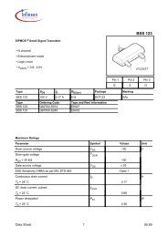
Rectifier diodes Schottky barrier
Rectifier diodes Schottky barrier
Rectifier diodes Schottky barrier

You also want an ePaper? Increase the reach of your titles
YUMPU automatically turns print PDFs into web optimized ePapers that Google loves.
Philips Semiconductors<br />
<strong>Rectifier</strong> <strong>diodes</strong><br />
<strong>Schottky</strong> <strong>barrier</strong><br />
Product specification<br />
BYV116, BYV116B series<br />
FEATURES SYMBOL QUICK REFERENCE DATA<br />
• Low forward volt drop<br />
• Fast switching<br />
• Reverse surge capability<br />
• High thermal cycling performance<br />
• Low thermal resistance<br />
a1<br />
a2<br />
1 3<br />
k 2<br />
V R = 20 V/ 25 V<br />
I O(AV) = 10 A<br />
V F ≤ 0.54 V<br />
GENERAL DESCRIPTION<br />
Dual schottky rectifier <strong>diodes</strong> intended for use as output rectifiers in low voltage, high frequency switched mode power<br />
supplies.<br />
The BYV116 series is supplied in the SOT78 (TO220AB) conventional leaded package.<br />
The BYV116B series is supplied in the SOT404 surface mounting package.<br />
PINNING SOT78 (TO220AB) SOT404<br />
PIN DESCRIPTION<br />
1 anode 1 (a)<br />
2 cathode (k) 1<br />
3 anode 2 (a)<br />
tab<br />
tab<br />
2<br />
tab<br />
cathode (k)<br />
123<br />
1 3<br />
LIMITING VALUES<br />
Limiting values in accordance with the Absolute Maximum System (IEC 134)<br />
SYMBOL PARAMETER CONDITIONS MIN. MAX. UNIT<br />
BYV118- 20 25<br />
BYV116B- 20 25<br />
V RRM Peak repetitive reverse - 20 25 V<br />
voltage<br />
V RWM Working peak reverse - 20 25 V<br />
voltage<br />
V R Continuous reverse voltage T mb ≤ 124 ˚C - 20 25 V<br />
I O(AV) Average rectified forward square wave; δ = 0.5; T mb ≤ 123 ˚C - 10 A<br />
current (both <strong>diodes</strong><br />
conducting)<br />
I FRM Repetitive peak forward square wave; δ = 0.5; T mb ≤ 123 ˚C - 10 A<br />
current per diode<br />
I FSM Non-repetitive peak forward t = 10 ms - 50 A<br />
current per diode t = 8.3 ms - 55 A<br />
sinusoidal; T j = 125 ˚C prior to<br />
surge; with reapplied V RRM(max)<br />
I RRM Peak repetitive reverse pulse width and repetition rate - 1 A<br />
surge current per diode limited by T j max<br />
T j Operating junction - 150 ˚C<br />
temperature<br />
T stg Storage temperature - 65 175 ˚C<br />
1. It is not possible to make connection to pin 2 of the SOT404 package.<br />
March 1998 1 Rev 1.000
Philips Semiconductors<br />
<strong>Rectifier</strong> <strong>diodes</strong><br />
<strong>Schottky</strong> <strong>barrier</strong><br />
Product specification<br />
BYV116, BYV116B series<br />
THERMAL RESISTANCES<br />
SYMBOL PARAMETER CONDITIONS MIN. TYP. MAX. UNIT<br />
R th j-mb Thermal resistance junction per diode - - 4 K/W<br />
to mounting base both <strong>diodes</strong> - - 3.5 K/W<br />
R th j-a Thermal resistance junction SOT78 package, in free air - 60 - K/W<br />
to ambient SOT404 package, pcb mounted, minimum - 50 - K/W<br />
footprint, FR4 board<br />
ELECTRICAL CHARACTERISTICS<br />
All characteristics are per diode at T j = 25 ˚C unless otherwise specified<br />
SYMBOL PARAMETER CONDITIONS MIN. TYP. MAX. UNIT<br />
V F Forward voltage I F = 5 A; T j = 125˚C - 0.47 0.54 V<br />
I F = 10 A; T j = 125˚C - 0.66 0.77 V<br />
I F = 5 A - 0.58 0.64 V<br />
I R Reverse current V R = V RWM - 0.05 3 mA<br />
V R = V RWM ; T j = 100˚C - 5 10 mA<br />
C d Junction capacitance V R = 5 V; f = 1 MHz, T j = 25˚C to 125˚C - 160 - pF<br />
March 1998 2 Rev 1.000
Philips Semiconductors<br />
<strong>Rectifier</strong> <strong>diodes</strong><br />
<strong>Schottky</strong> <strong>barrier</strong><br />
Product specification<br />
BYV116, BYV116B series<br />
5<br />
4<br />
3<br />
Forward dissipation, PF (W)<br />
Vo = 0.31 V<br />
Rs = 0.046 Ohms<br />
0.1<br />
0.2<br />
BYV116<br />
0.5<br />
Tmb(max) / C<br />
130<br />
D = 1.0<br />
134<br />
138<br />
IR / A<br />
100mA<br />
150 C<br />
10mA<br />
125 C<br />
100 C<br />
1mA<br />
BYV116<br />
2<br />
1<br />
I tp<br />
D =<br />
t<br />
T<br />
0<br />
150<br />
0 1 2 3 4 5 6 7 8<br />
Average forward current, IF(AV) (A)<br />
Fig.1. Maximum forward dissipation P F = f(I F(AV) ) per<br />
diode; square current waveform where<br />
I F(AV) =I F(RMS) x √D.<br />
tp<br />
T<br />
142<br />
146<br />
100uA<br />
10uA<br />
75 C<br />
50 C<br />
Tj = 25 C<br />
1uA<br />
0 5 10 15 20 25<br />
VR / V<br />
Fig.4. Typical reverse leakage current per diode;<br />
I R = f(V R ); parameter T j<br />
5<br />
4<br />
3<br />
Forward dissipation, PF (W)<br />
Vo = 0.31 V<br />
Rs = 0.046 Ohms<br />
4<br />
2.8<br />
BYV116<br />
2.2<br />
Tmb(max) / C<br />
130<br />
1.9<br />
a = 1.57 134<br />
138<br />
Cd / pF<br />
1000<br />
BYV116<br />
100<br />
2<br />
142<br />
1<br />
146<br />
0<br />
150<br />
0 1 2 3 4 5<br />
Average forward current, IF(AV) (A)<br />
Fig.2. Maximum forward dissipation P F = f(I F(AV) ) per<br />
diode; sinusoidal current waveform where a = form<br />
factor = I F(RMS) / I F(AV) .<br />
10<br />
1 10 100<br />
VR / V<br />
Fig.5. Typical junction capacitance per diode;<br />
C d = f(V R ); f = 1 MHz; T j = 25˚C to 125 ˚C.<br />
IF / A<br />
10<br />
Tj = 25 C<br />
Tj = 125 C<br />
8<br />
BYV116<br />
10<br />
1<br />
Transient thermal impedance, Zth j-mb (K/W)<br />
6<br />
typ<br />
max<br />
0.1<br />
4<br />
2<br />
0.01<br />
P<br />
D<br />
tp<br />
D =<br />
T<br />
tp<br />
0<br />
0 0.2 0.4 0.6 0.8 1<br />
VF / V<br />
Fig.3. Typical and maximum forward characteristic<br />
I F = f(V F ); parameter T j<br />
t<br />
T<br />
0.001<br />
1us 10us 100us 1ms 10ms 100ms 1s 10s<br />
pulse width, tp (s) PBYR325CTD<br />
Fig.6. Transient thermal impedance; per diode;<br />
Z th j-mb = f(t p ).<br />
March 1998 3 Rev 1.000
Philips Semiconductors<br />
<strong>Rectifier</strong> <strong>diodes</strong><br />
<strong>Schottky</strong> <strong>barrier</strong><br />
Product specification<br />
BYV116, BYV116B series<br />
MECHANICAL DATA<br />
Dimensions in mm<br />
Net Mass: 1.4 g<br />
10.3 max<br />
4.5 max<br />
1.4 max<br />
11 max<br />
15.4<br />
2.5<br />
2.54 (x2)<br />
MOUNTING INSTRUCTIONS<br />
0.85 max<br />
(x2)<br />
Fig.7. SOT404 : centre pin connected to mounting base.<br />
0.5<br />
Dimensions in mm<br />
11.5<br />
9.0<br />
17.5<br />
2.0<br />
3.8<br />
5.08<br />
Fig.8. SOT404 : minimum pad sizes for surface mounting.<br />
Notes<br />
1. Plastic meets UL94 V0 at 1/8".<br />
March 1998 4 Rev 1.000
Philips Semiconductors<br />
<strong>Rectifier</strong> <strong>diodes</strong><br />
<strong>Schottky</strong> <strong>barrier</strong><br />
Product specification<br />
BYV116, BYV116B series<br />
MECHANICAL DATA<br />
Dimensions in mm<br />
Net Mass: 2 g<br />
4,5<br />
max<br />
10,3<br />
max<br />
3,7<br />
1,3<br />
2,8<br />
5,9<br />
min<br />
15,8<br />
max<br />
3,0 max<br />
not tinned<br />
1,3<br />
max<br />
(2x)<br />
1 2 3<br />
2,54 2,54<br />
3,0<br />
13,5<br />
min<br />
0,9 max (3x)<br />
0,6<br />
2,4<br />
Notes<br />
1. Refer to mounting instructions for SOT78 (TO220) envelopes.<br />
2. Epoxy meets UL94 V0 at 1/8".<br />
Fig.9. SOT78 (TO220AB); pin 2 connected to mounting base.<br />
March 1998 5 Rev 1.000
Philips Semiconductors<br />
<strong>Rectifier</strong> <strong>diodes</strong><br />
<strong>Schottky</strong> <strong>barrier</strong><br />
Product specification<br />
BYV116, BYV116B series<br />
DEFINITIONS<br />
Data sheet status<br />
Objective specification This data sheet contains target or goal specifications for product development.<br />
Preliminary specification This data sheet contains preliminary data; supplementary data may be published later.<br />
Product specification This data sheet contains final product specifications.<br />
Limiting values<br />
Limiting values are given in accordance with the Absolute Maximum Rating System (IEC 134). Stress above one<br />
or more of the limiting values may cause permanent damage to the device. These are stress ratings only and<br />
operation of the device at these or at any other conditions above those given in the Characteristics sections of<br />
this specification is not implied. Exposure to limiting values for extended periods may affect device reliability.<br />
Application information<br />
Where application information is given, it is advisory and does not form part of the specification.<br />
© Philips Electronics N.V. 1998<br />
All rights are reserved. Reproduction in whole or in part is prohibited without the prior written consent of the<br />
copyright owner.<br />
The information presented in this document does not form part of any quotation or contract, it is believed to be<br />
accurate and reliable and may be changed without notice. No liability will be accepted by the publisher for any<br />
consequence of its use. Publication thereof does not convey nor imply any license under patent or other<br />
industrial or intellectual property rights.<br />
LIFE SUPPORT APPLICATIONS<br />
These products are not designed for use in life support appliances, devices or systems where malfunction of these<br />
products can be reasonably expected to result in personal injury. Philips customers using or selling these products<br />
for use in such applications do so at their own risk and agree to fully indemnify Philips for any damages resulting<br />
from such improper use or sale.<br />
March 1998 6 Rev 1.000