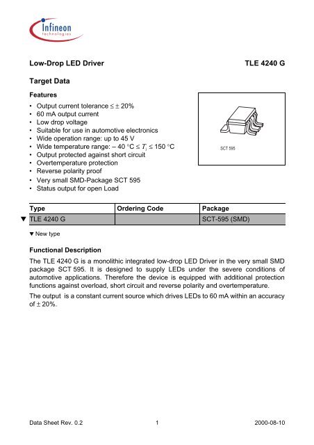
Low-Drop LED Driver Target Data TLE 4240 G
Low-Drop LED Driver Target Data TLE 4240 G
Low-Drop LED Driver Target Data TLE 4240 G

You also want an ePaper? Increase the reach of your titles
YUMPU automatically turns print PDFs into web optimized ePapers that Google loves.
<strong>Low</strong>-<strong>Drop</strong> <strong>LED</strong> <strong>Driver</strong><br />
<strong>TLE</strong> <strong>4240</strong> G<br />
<strong>Target</strong> <strong>Data</strong><br />
Features<br />
• Output current tolerance ≤ ± 20%<br />
• 60 mA output current<br />
• <strong>Low</strong> drop voltage<br />
• Suitable for use in automotive electronics<br />
• Wide operation range: up to 45 V<br />
• Wide temperature range: – 40 °C ≤ T j ≤ 150 °C<br />
• Output protected against short circuit<br />
• Overtemperature protection<br />
• Reverse polarity proof<br />
• Very small SMD-Package SCT 595<br />
• Status output for open Load<br />
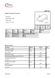
SCT 595<br />
Type Ordering Code Package<br />
▼ <strong>TLE</strong> <strong>4240</strong> G<br />
SCT-595 (SMD)<br />
▼ New type<br />
Functional Description<br />
The <strong>TLE</strong> <strong>4240</strong> G is a monolithic integrated low-drop <strong>LED</strong> <strong>Driver</strong> in the very small SMD<br />
package SCT 595. It is designed to supply <strong>LED</strong>s under the severe conditions of<br />
automotive applications. Therefore the device is equipped with additional protection<br />
functions against overload, short circuit and reverse polarity and overtemperature.<br />
The output is a constant current source which drives <strong>LED</strong>s to 60 mA within an accuracy<br />
of ± 20%.<br />
<strong>Data</strong> Sheet Rev. 0.2 1 2000-08-10
<strong>TLE</strong> <strong>4240</strong> G<br />
Pin Configuration<br />
(top view)<br />
ST<br />
1<br />
5<br />
GND<br />
GND<br />
2<br />
Ι<br />
3<br />
4<br />
Q<br />
AEP02906<br />
Figure 1<br />
Pin Definitions and Functions<br />
Pin No. Symbol Function<br />
1 ST Status output; low level for open load<br />
2 GND Ground; internally connected to pin 5<br />
3 I Input voltage<br />
4 Q Output<br />
5 GND Ground<br />
<strong>Data</strong> Sheet Rev. 0.2 2 2000-08-10
<strong>TLE</strong> <strong>4240</strong> G<br />
<strong>TLE</strong> <strong>4240</strong> G<br />
I 3 4 1<br />
Control<br />
Amplifier<br />
Buffer<br />
Q<br />
Temperature<br />
Sensor<br />
> 66 mA<br />
Current<br />
Limit<br />
< 1 mA<br />
Control<br />
2, 5<br />
GND<br />
ST<br />
AEB03001<br />
Figure 2<br />
Block Diagram<br />
<strong>Data</strong> Sheet Rev. 0.2 3 2000-08-10
<strong>TLE</strong> <strong>4240</strong> G<br />
Absolute Maximum Ratings<br />
– 40 °C < T j < 150 °C<br />
Parameter Symbol Limit Values Unit Remarks<br />
min. max.<br />
Input<br />
Voltage V I –42 45 V –<br />
Current I I – – mA internally limited<br />
Output<br />
Voltage V Q – 1 40 V –<br />
Current I Q – – mA internally limited<br />
Status<br />
Voltage V ST – 0.3 40 V –<br />
Current I ST – 5 5 mA internally limited<br />
Temperatures<br />
Junction temperature T j – 40 150 °C –<br />
Storage temperature T stg – 50 150 °C –<br />
Thermal Resistances<br />
Junction ambient R thja – 179 K/W zero heat sink area,<br />
zero airflow<br />
Note: Maximum ratings are absolute ratings; exceeding any one of these values may<br />
cause irreversible damage to the integrated circuit.<br />
<strong>Data</strong> Sheet Rev. 0.2 4 2000-08-10
<strong>TLE</strong> <strong>4240</strong> G<br />
Operating Range<br />
Parameter Symbol Limit Values Unit Remarks<br />
min. max.<br />
Input voltage V I 3 45 V –<br />
Status output voltage V ST – 7 V –<br />
Junction temperature T j – 40 150 °C –<br />
Electrical Characteristics<br />
V I = 13.5 V; – 40 °C
<strong>TLE</strong> <strong>4240</strong> G<br />
Current Consumption I q versus<br />
Output Current I Q<br />
Ι Q<br />
AED02908<br />
7<br />
mA<br />
6<br />
5<br />
4<br />
3<br />
2<br />
1<br />
0<br />
0 10 20 30 40 50 mA 60<br />
Ι<br />
Q<br />
Output Current I Q versus<br />
Input Voltage V I<br />
AED02745<br />
120<br />
Ι mA Q<br />
100<br />
80<br />
T j<br />
= 25 ˚C<br />
60<br />
40<br />
T j<br />
= 125 ˚C<br />
20<br />
0<br />
0<br />
10 20 30 40 V 50<br />
V I<br />
<strong>Data</strong> Sheet Rev. 0.2 6 2000-08-10
<strong>TLE</strong> <strong>4240</strong> G<br />
Package Outlines<br />
SCT-595<br />
(Special Package)<br />
(0.13)<br />
B<br />
+0.1<br />
1.2 -0.05<br />
(0.23) 1)<br />
(0.4) 1)<br />
+0.1<br />
0.6 -0.05<br />
2.9 ±0.2<br />
(2.2)<br />
(0.3)<br />
+0.1<br />
0.3 -0.05<br />
0.95<br />
+0.2<br />
acc. to<br />
DIN 6784<br />
2.6 max<br />
0.25 min<br />
10˚max<br />
0.20<br />
M<br />
1.1 max<br />
A<br />
0.1 max<br />
+0.1<br />
0.15 -0.06<br />
10˚max<br />
1.6 ±0.1<br />
A<br />
1.9<br />
0.25 M B<br />
1) Contour of slot depends on profile<br />
of gull-wing lead form<br />
Sorts of Packing<br />
Package outlines for tubes, trays etc. are contained in our<br />
<strong>Data</strong> Book “Package Information”.<br />
SMD = Surface Mounted Device<br />
Dimensions in mm<br />
<strong>Data</strong> Sheet Rev. 0.2 7 2000-08-10
<strong>TLE</strong> <strong>4240</strong> G<br />
Edition 2000-08-10<br />
Published by Infineon Technologies AG,<br />
St.-Martin-Strasse 53,<br />
D-81541 München, Germany<br />
© Infineon Technologies AG 8/18/00.<br />
All Rights Reserved.<br />
Attention please!<br />
The information herein is given to describe<br />
certain components and shall not be considered<br />
as warranted characteristics.<br />
Terms of delivery and rights to technical<br />
change reserved.<br />
We hereby disclaim any and all warranties,<br />
including but not limited to warranties of<br />
non-infringement, regarding circuits, descriptions<br />
and charts stated herein.<br />
Infineon Technologies is an approved CECC<br />
manufacturer.<br />
Information<br />
For further information on technology, delivery<br />
terms and conditions and prices please<br />
contact your nearest Infineon Technologies<br />
Office in Germany or our Infineon Technologies<br />
Representatives worldwide (see address<br />
list).<br />
Warnings<br />
Due to technical requirements components<br />
may contain dangerous substances. For information<br />
on the types in question please<br />
contact your nearest Infineon Technologies<br />
Office.<br />
Infineon Technologies Components may only<br />
be used in life-support devices or systems<br />
with the express written approval of Infineon<br />
Technologies, if a failure of such components<br />
can reasonably be expected to cause the failure<br />
of that life-support device or system, or to<br />
affect the safety or effectiveness of that device<br />
or system. Life support devices or systems<br />
are intended to be implanted in the human<br />
body, or to support and/or maintain and<br />
sustain and/or protect human life. If they fail,<br />
it is reasonable to assume that the health of<br />
the user or other persons may be endangered.<br />
<strong>Data</strong> Sheet Rev. 0.2 8 2000-08-10