PICMG COM Express Carrier Design Guide
PICMG COM Express Carrier Design Guide
PICMG COM Express Carrier Design Guide

Create successful ePaper yourself
Turn your PDF publications into a flip-book with our unique Google optimized e-Paper software.
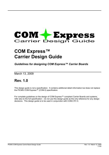
<strong>COM</strong> <strong>Express</strong><br />
<strong>Carrier</strong> <strong>Design</strong> <strong>Guide</strong><br />
<strong>Guide</strong>lines for designing <strong>COM</strong> <strong>Express</strong> <strong>Carrier</strong> Boards<br />
March 13, 2009<br />
Rev. 1.0<br />
This design guide is not a specification. It contains additional detail information but does not replace<br />
the <strong>PICMG</strong> <strong>COM</strong> <strong>Express</strong> (<strong>COM</strong>.0) specification.<br />
For complete guidelines on the design of <strong>COM</strong> <strong>Express</strong> compliant <strong>Carrier</strong> Boards and systems,<br />
refer also to the full specification – do not use this design guide as the only reference for any design<br />
decisions. This design guide is to be used in conjunction with <strong>COM</strong>.0 R1.0.<br />
<strong>PICMG</strong> <strong>COM</strong> <strong>Express</strong> <strong>Carrier</strong> Board <strong>Design</strong> <strong>Guide</strong> Rev. 1.0 / March 13, 2009<br />
1/160
©Copyright 2008, PCI Industrial Computer Manufacturers Group.<br />
The attention of adopters is directed to the possibility that compliance with or adoption of<br />
<strong>PICMG</strong> ® specifications may require use of an invention covered by patent rights. <strong>PICMG</strong> ® shall<br />
not be responsible for identifying patents for which a license may be required by any <strong>PICMG</strong> ®<br />
specification or for conducting legal inquiries into the legal validity or scope of those patents that<br />
are brought to its attention. <strong>PICMG</strong> ® specifications are prospective and advisory only.<br />
Prospective users are responsible for protecting themselves against liability for infringement of<br />
patents.<br />
NOTICE:<br />
The information contained in this document is subject to change without notice. The material in<br />
this document details a <strong>PICMG</strong> ® specification in accordance with the license and notices set forth<br />
on this page. This document does not represent a commitment to implement any portion of this<br />
specification in any company's products.<br />
WHILE THE INFORMATION IN THIS PUBLICATION IS BELIEVED TO BE ACCURATE, <strong>PICMG</strong> ®<br />
MAKES NO WARRANTY OF ANY KIND, EXPRESS OR IMPLIED, WITH REGARD TO THIS<br />
MATERIAL INCLUDING, BUT NOT LIMITED TO, ANY WARRANTY OF TITLE OR<br />
OWNERSHIP, IMPLIED WARRANTY OF MERCHANTABILITY OR WARRANTY OF FITNESS<br />
FOR PARTICULAR PURPOSE OR USE.<br />
In no event shall <strong>PICMG</strong> ® be liable for errors contained herein or for indirect, incidental, special,<br />
consequential, reliance or cover damages, including loss of profits, revenue, data or use,<br />
incurred by any user or any third party. Compliance with this specification does not absolve<br />
manufacturers of CompactPCI ® <strong>Express</strong> equipment from the requirements of safety and<br />
regulatory agencies (UL, CSA, FCC, IEC, etc.).<br />
<strong>PICMG</strong> ® , CompactPCI ® , AdvancedTCA ® , ATCA ® , CompactPCI ® <strong>Express</strong> and the <strong>PICMG</strong>,<br />
CompactPCI, AdvancedTCA and ATCA logos are registered trademarks, and <strong>COM</strong> <strong>Express</strong>,<br />
MicroTCA, μTCA, CompactTCA, AdvancedTCA300, AdvancedMC and SHB<br />
<strong>Express</strong> are trademarks, of the PCI Industrial Computer Manufacturers Group. All other brand<br />
or product names may be trademarks or registered trademarks of their respective holders.<br />
<strong>PICMG</strong> <strong>COM</strong> <strong>Express</strong> <strong>Carrier</strong> Board <strong>Design</strong> <strong>Guide</strong> Rev. 1.0 / March 13, 2009<br />
2/160
Contents<br />
1. Preface..................................................................................................................................8<br />
1.1. About This Document...........................................................................................................8<br />
1.2. Intended Audience................................................................................................................8<br />
1.3. No special word usage.........................................................................................................8<br />
1.4. No statements of compliance..............................................................................................8<br />
1.5. Correctness Disclaimer........................................................................................................8<br />
1.6. Name and logo usage...........................................................................................................9<br />
1.7. Intellectual property............................................................................................................10<br />
1.8. Copyright Notice.................................................................................................................11<br />
1.9. Acronyms and Abbreviations Used...................................................................................12<br />
1.10. Signal Table Terminology...................................................................................................13<br />
2. <strong>COM</strong> <strong>Express</strong> Interfaces....................................................................................................15<br />
2.1. <strong>COM</strong> <strong>Express</strong> Signals.........................................................................................................15<br />
2.2. PCIe General Introduction..................................................................................................17<br />
2.2.1. <strong>COM</strong> <strong>Express</strong> A-B Connector and C-D Connector PCIe Groups....................................17<br />
2.3. General Purpose PCIe Lanes.............................................................................................18<br />
2.3.1. General Purpose PCIe Signal Definitions.......................................................................18<br />
2.3.2. PCI <strong>Express</strong> Lane Configurations – Per <strong>COM</strong> <strong>Express</strong> Spec.........................................19<br />
2.3.3. PCI <strong>Express</strong> Lane Configurations – Module and Chipset Dependencies.......................19<br />
2.3.4. Device Up / Device Down and PCIe Rx / Tx Coupling Capacitors..................................20<br />
2.3.5. Schematic Examples.......................................................................................................21<br />
2.3.5.1. Reference Clock Buffer..........................................................................................21<br />
2.3.5.2. Reset...................................................................................................................... 23<br />
2.3.5.3. x1 Slot Example.....................................................................................................23<br />
2.3.5.4. x4 Slot Example.....................................................................................................24<br />
2.3.5.5. PCIe x1 Generic Device Down Example................................................................25<br />
2.3.5.6. PCIe x4 Generic Device Down Example................................................................26<br />
2.3.5.7. PCI <strong>Express</strong> Mini Card...........................................................................................27<br />
2.3.5.8. <strong>Express</strong>Card...........................................................................................................29<br />
2.3.6. PCI <strong>Express</strong> Routing Considerations..............................................................................32<br />
2.3.6.1. Polarity Inversion....................................................................................................32<br />
2.3.6.2. Lane Reversal........................................................................................................32<br />
2.4. PEG (PCI <strong>Express</strong> Graphics)..............................................................................................33<br />
2.4.1. Signal Definitions.............................................................................................................33<br />
2.4.2. PEG Configuration...........................................................................................................34<br />
2.4.2.1. Using PEG Pins for an External Graphics Card......................................................35<br />
2.4.2.2. Using PEG Pins for SDVO.....................................................................................35<br />
2.4.2.3. Using PEG Pins for General Purpose PCIe Lanes.................................................35<br />
2.4.3. Reference Schematics.....................................................................................................37<br />
2.4.3.1. x1, x4, x8, x16 Slot.................................................................................................37<br />
2.4.4. Routing Considerations...................................................................................................38<br />
2.4.4.1. Polarity Inversion....................................................................................................38<br />
2.4.4.2. Lane Reversal........................................................................................................38<br />
2.5. SDVO....................................................................................................................................40<br />
2.5.1. Signal Definitions.............................................................................................................40<br />
2.5.1.1. SDVO Port Configuration........................................................................................40<br />
2.5.1.2. Supported SDVO Devices......................................................................................41<br />
2.5.2. Reference Schematics.....................................................................................................42<br />
<strong>PICMG</strong> <strong>COM</strong> <strong>Express</strong> <strong>Carrier</strong> Board <strong>Design</strong> <strong>Guide</strong> Rev. 1.0 / March 13, 2009<br />
3/160
2.5.2.1. SDVO to DVI Transmitter Example........................................................................42<br />
2.5.2.2. Other SDVO Output Options: LVDS, NTSC............................................................43<br />
2.5.3. Routing Considerations...................................................................................................44<br />
2.5.3.1. SDVO Option – PEG Lane Reversal......................................................................44<br />
2.6. LAN.......................................................................................................................................45<br />
2.6.1. Signal Definitions.............................................................................................................45<br />
2.6.1.1. Status LED Signal Definitions.................................................................................45<br />
2.6.1.2. LAN 1 and 2 shared with IDE.................................................................................46<br />
2.6.1.3. PHY / Magnetics Connections................................................................................46<br />
2.6.2. Reference Schematics.....................................................................................................48<br />
2.6.2.1. Magnetics Integrated Into RJ-45 Receptacle..........................................................48<br />
2.6.2.2. Discrete Coupling Transformer...............................................................................49<br />
2.6.3. Routing Considerations...................................................................................................50<br />
2.6.3.1. Reference Ground Isolation and Coupling..............................................................50<br />
2.7. USB Ports............................................................................................................................51<br />
2.7.1. Signal Definitions.............................................................................................................51<br />
2.7.1.1. USB Over-Current Protection (USB_x_y_OC#)......................................................51<br />
2.7.1.2. Powering USB devices during S5...........................................................................51<br />
2.7.1.3. USB connector.......................................................................................................52<br />
2.7.2. Reference Schematics.....................................................................................................52<br />
2.7.3. Routing Considerations...................................................................................................55<br />
2.7.3.1. EMI / ESD Protection .............................................................................................55<br />
2.8. SATA.....................................................................................................................................56<br />
2.8.1. Signal Definitions.............................................................................................................56<br />
2.8.2. Reference Schematic......................................................................................................58<br />
2.8.3. Routing Considerations...................................................................................................59<br />
2.9. LVDS.....................................................................................................................................60<br />
2.9.1. Signal Definitions.............................................................................................................60<br />
2.9.1.1. Connector and Cable Considerations.....................................................................61<br />
2.9.1.2. Display Timing Configuration..................................................................................61<br />
2.9.1.3. Backlight Control....................................................................................................61<br />
2.9.1.4. Color Mapping and Terms......................................................................................62<br />
2.9.1.5. Note on Industry Terms..........................................................................................63<br />
2.9.1.6. LVDS Display Color Mapping Tables......................................................................64<br />
2.9.2. Reference Schematics.....................................................................................................66<br />
2.9.3. Routing Considerations...................................................................................................67<br />
2.10. IDE and CompactFlash (PATA)...........................................................................................68<br />
2.10.1. Signal Definitions.............................................................................................................68<br />
2.10.2. IDE 40-Pin Header (3.5 Inch Drives)...............................................................................69<br />
2.10.3. IDE 44-Pin Header (2.5 Inch and Low Profile Optical Drives).........................................69<br />
2.10.4. CompactFlash 50 Pin Header.........................................................................................69<br />
2.10.5. IDE / CompactFlash Reference Schematics...................................................................69<br />
2.10.6. Routing Considerations...................................................................................................70<br />
2.11. VGA......................................................................................................................................71<br />
2.11.1. Signal Definitions.............................................................................................................71<br />
2.11.2. VGA Connector................................................................................................................71<br />
2.11.3. VGA Reference Schematics............................................................................................72<br />
2.11.4. Routing Considerations...................................................................................................73<br />
2.11.4.1. RGB Analog Signals...............................................................................................73<br />
2.11.4.2. HSYNC and VSYNC Signals..................................................................................73<br />
2.11.4.3. DDC Interface.........................................................................................................73<br />
2.11.4.4. ESD Protection/EMI................................................................................................73<br />
<strong>PICMG</strong> <strong>COM</strong> <strong>Express</strong> <strong>Carrier</strong> Board <strong>Design</strong> <strong>Guide</strong> Rev. 1.0 / March 13, 2009<br />
4/160
2.12. TV-Out..................................................................................................................................74<br />
2.12.1. Signal Definitions.............................................................................................................74<br />
2.12.2. TV-Out Connector............................................................................................................74<br />
2.12.3. TV-Out Reference Schematics........................................................................................76<br />
2.12.4. Routing Considerations...................................................................................................77<br />
2.12.4.1. Signal Termination..................................................................................................77<br />
2.12.4.2. Video Filter.............................................................................................................77<br />
2.12.4.3. ESD Protection.......................................................................................................77<br />
2.13. AC'97 and HDA Digital Audio Interfaces............................................................................78<br />
2.13.1. Signal Definitions.............................................................................................................78<br />
2.13.2. Reference Schematics.....................................................................................................80<br />
2.13.2.1. AC'97...................................................................................................................... 80<br />
2.13.2.2. High Definition Audio (HDA)...................................................................................82<br />
2.13.3. Routing Considerations...................................................................................................83<br />
2.14. PCI Bus................................................................................................................................84<br />
2.14.1. Signal Definitions.............................................................................................................84<br />
2.14.2. Reference Schematics.....................................................................................................85<br />
2.14.2.1. Resource Allocation................................................................................................85<br />
2.14.2.2. Device-Down Example...........................................................................................87<br />
2.14.2.3. Device-Down Considerations.................................................................................88<br />
2.14.2.4. Clock Buffer............................................................................................................88<br />
2.14.3. Routing Considerations...................................................................................................88<br />
2.14.3.1. General PCI Signals...............................................................................................88<br />
2.14.3.2. PCI Clock Routing..................................................................................................88<br />
2.15. LPC Bus – Low Pin Count Interface..................................................................................90<br />
2.15.1. Signal Definition...............................................................................................................90<br />
2.15.2. LPC Bus Reference Schematics.....................................................................................90<br />
2.15.2.1. LPC Bus Clock Signal............................................................................................90<br />
2.15.2.2. LPC Reset Signal...................................................................................................91<br />
2.15.2.3. LPC Firmware Hub.................................................................................................92<br />
2.15.2.4. LPC PLD Example – Port 80 Decoder....................................................................94<br />
2.15.2.5. SuperIO.................................................................................................................. 95<br />
2.15.3. Routing Considerations...................................................................................................96<br />
2.15.3.1. General Signals......................................................................................................96<br />
2.15.3.2. Bus Clock Routing..................................................................................................96<br />
2.16. General Purpose I2C Bus Interface...................................................................................98<br />
2.16.1. Signal Definitions.............................................................................................................98<br />
2.16.2. Reference Schematics.....................................................................................................98<br />
2.16.3. Routing Considerations...................................................................................................99<br />
2.17. System Management Bus (SMBus).................................................................................100<br />
2.17.1. Signal Definitions...........................................................................................................100<br />
2.17.2. Reference Schematics..................................................................................................101<br />
2.17.3. Routing Considerations.................................................................................................101<br />
2.18. Miscellaneous Signals......................................................................................................102<br />
2.18.1. Module Type Detection..................................................................................................102<br />
2.18.2. Speaker Output..............................................................................................................103<br />
2.18.3. RTC Battery Implementation.........................................................................................104<br />
2.18.3.1. RTC Battery Lifetime............................................................................................104<br />
2.18.4. Power Management Signals..........................................................................................105<br />
2.18.5. Watchdog Timer.............................................................................................................107<br />
2.18.6. General Purpose Input/Output (GPIO)..........................................................................108<br />
<strong>PICMG</strong> <strong>COM</strong> <strong>Express</strong> <strong>Carrier</strong> Board <strong>Design</strong> <strong>Guide</strong> Rev. 1.0 / March 13, 2009<br />
5/160
2.18.7. Thermal Interface...........................................................................................................110<br />
3. Power and Reset..............................................................................................................111<br />
3.1. General Power requirements............................................................................................111<br />
3.1.1. VCC_12V Rise Time Caution and Inrush Currents........................................................111<br />
3.2. ATX and AT Style Power Control......................................................................................112<br />
3.2.1. ATX vs AT Supplies........................................................................................................112<br />
3.2.2. Power States..................................................................................................................112<br />
3.2.3. ATX and AT Power Sequencing Diagrams....................................................................113<br />
3.2.4. Power Monitoring Circuit Discussion.............................................................................116<br />
3.2.5. Power Button..................................................................................................................117<br />
3.3. Reference Schematics......................................................................................................118<br />
3.3.1. ATX Power Supply.........................................................................................................118<br />
3.3.1.1. Minimum Loads....................................................................................................120<br />
3.4. Routing Considerations....................................................................................................121<br />
3.4.1. VCC_12V and GND.......................................................................................................121<br />
3.4.2. Copper Trace Sizing and Current Capacity...................................................................121<br />
3.4.3. VCC5_SBY Routing.......................................................................................................122<br />
3.4.4. Power State and Reset Signal Routing.........................................................................122<br />
3.4.5. Slot Card Supply Decoupling Recommendations.........................................................123<br />
4. BIOS Considerations.......................................................................................................124<br />
4.1. Legacy versus Legacy-Free.............................................................................................124<br />
4.2. Super I/O............................................................................................................................124<br />
5. <strong>COM</strong> <strong>Express</strong> Module Connectors.................................................................................125<br />
5.1. Connector Descriptions....................................................................................................125<br />
5.2. Connector Land Patterns and Alignment........................................................................125<br />
5.3. Connector and Module CAD Symbol Recommendations..............................................125<br />
6. <strong>Carrier</strong> Board PCB Layout <strong>Guide</strong>lines...........................................................................126<br />
6.1. General...............................................................................................................................126<br />
6.2. PCB Stack-ups..................................................................................................................126<br />
6.2.1. Four-Layer Stack-up......................................................................................................126<br />
6.2.2. Six-Layer Stack-up........................................................................................................126<br />
6.2.3. Eight-Layer Stack-up.....................................................................................................127<br />
6.3. Trace-Impedance Considerations....................................................................................128<br />
6.4. Routing Rules for High-Speed Differential Interfaces....................................................130<br />
6.4.1. PCI <strong>Express</strong> 1.1 Trace Routing <strong>Guide</strong>lines...................................................................132<br />
6.4.2. USB Trace Routing <strong>Guide</strong>lines......................................................................................133<br />
6.4.3. PEG 1.1 Trace Routing <strong>Guide</strong>lines................................................................................134<br />
6.4.4. SDVO Trace Routing <strong>Guide</strong>lines...................................................................................135<br />
6.4.5. LAN Trace Routing <strong>Guide</strong>lines......................................................................................136<br />
6.4.6. Serial ATA Trace Routing <strong>Guide</strong>lines.............................................................................137<br />
6.4.7. LVDS Trace Routing <strong>Guide</strong>lines....................................................................................138<br />
6.5. Routing Rules for Single Ended Interfaces.....................................................................139<br />
6.5.1. PCI Trace Routing <strong>Guide</strong>lines.......................................................................................140<br />
<strong>PICMG</strong> <strong>COM</strong> <strong>Express</strong> <strong>Carrier</strong> Board <strong>Design</strong> <strong>Guide</strong> Rev. 1.0 / March 13, 2009<br />
6/160
6.5.2. IDE Trace Routing <strong>Guide</strong>lines.......................................................................................141<br />
6.5.3. LPC Trace Routing <strong>Guide</strong>lines......................................................................................142<br />
7. Mechanical Considerations............................................................................................143<br />
7.1. Form Factors.....................................................................................................................143<br />
7.2. Heatspreader.....................................................................................................................144<br />
7.2.1. Top mounting.................................................................................................................145<br />
7.2.2. Bottom mounting............................................................................................................146<br />
7.2.3. Materials........................................................................................................................146<br />
8. Applicable Documents and Standards..........................................................................148<br />
8.1. Technology Specifications...............................................................................................148<br />
8.2. Regulatory Specifications................................................................................................150<br />
8.3. Useful books......................................................................................................................151<br />
Appendix A: Sourcecode for Port 80 Decoder..............................................................152<br />
Appendix B: List of Tables..............................................................................................156<br />
Appendix C: List of Figures............................................................................................158<br />
Appendix D: Revision History.........................................................................................160<br />
<strong>PICMG</strong> <strong>COM</strong> <strong>Express</strong> <strong>Carrier</strong> Board <strong>Design</strong> <strong>Guide</strong> Rev. 1.0 / March 13, 2009<br />
7/160
Preface<br />
1. Preface<br />
1.1. About This Document<br />
This document provides information for designing a custom system <strong>Carrier</strong> Board for <strong>COM</strong><br />
<strong>Express</strong> Modules. It includes reference schematics for the external circuitry required to<br />
implement the various <strong>COM</strong> <strong>Express</strong> peripheral functions. It also explains how to extend the<br />
supported buses and how to add additional peripherals and expansion slots to a <strong>COM</strong> <strong>Express</strong><br />
based system.<br />
It's strongly recommended to use the latest <strong>COM</strong> <strong>Express</strong> specification and the Module vendors'<br />
product manuals as a reference.<br />
This design guide is not a specification. It contains additional detail information but does<br />
not replace the <strong>PICMG</strong> <strong>COM</strong> <strong>Express</strong> (<strong>COM</strong>.0) specification.<br />
For complete guidelines on the design of <strong>COM</strong> <strong>Express</strong> compliant <strong>Carrier</strong> Boards and systems,<br />
refer also to the full specification – do not use this design guide as the only reference for any<br />
design decisions.<br />
1.2. Intended Audience<br />
This design guide is intended for electronics engineers and PCB layout engineers designing<br />
<strong>Carrier</strong> Boards for <strong>PICMG</strong> <strong>COM</strong> <strong>Express</strong> Modules.<br />
1.3. No special word usage<br />
Unlike a <strong>PICMG</strong> specification, which assigns special meanings to certain words such as ”shall”,<br />
“should” and “may”, there is no such usage in this document. That is because this document is<br />
not a specification; it is a non-normative design guide.<br />
1.4. No statements of compliance<br />
As this document is not a specification but a set of guidelines, there should not be any<br />
statements of compliance made with reference to this document.<br />
1.5. Correctness Disclaimer<br />
The schematic examples given in this document are believed to be correct but no guarantee is<br />
given. In most cases, the examples come from designs that have been built and tested.<br />
<strong>PICMG</strong> <strong>COM</strong> <strong>Express</strong> <strong>Carrier</strong> Board <strong>Design</strong> <strong>Guide</strong> Rev. 1.0 / March 13, 2009<br />
8/160
Preface<br />
1.6. Name and logo usage<br />
The PCI Industrial Computer Manufacturers Group’s policies regarding the use of its logos and<br />
trademarks are as follows:<br />
Permission to use the <strong>PICMG</strong> organization logo is automatically granted to designated members<br />
only as stipulated on the most recent Membership Privileges document (available at<br />
www.picmg.org) during the period of time for which their membership dues are paid.<br />
Nonmembers must not use the <strong>PICMG</strong> organization logo.<br />
The <strong>PICMG</strong> organization logo must be printed in black or color as shown in the files available for<br />
download from the member’s side of the Web site. Logos with or without the “Open Modular<br />
Computing Specifications” banner can be used. Nothing may be added or deleted from the<br />
<strong>PICMG</strong> logo.<br />
The use of the <strong>COM</strong> <strong>Express</strong> logo is a privilege granted by the <strong>PICMG</strong> ® organization to<br />
companies who have purchased the relevant specifications (or acquired them as a member<br />
benefit), and that believe their products comply with these specifications. Manufacturers'<br />
distributors and sales representatives may use the <strong>COM</strong> <strong>Express</strong> logo in promoting products sold<br />
under the name of the manufacturer. Use of the logos by either members or non-members<br />
implies such compliance. Only <strong>PICMG</strong> Executive and Associate members may use the <strong>PICMG</strong> ®<br />
logo. <strong>PICMG</strong> ® may revoke permission to use logos if they are misused. The <strong>COM</strong> <strong>Express</strong> logo<br />
can be found on the <strong>PICMG</strong> web site, www.picmg.org.<br />
The <strong>PICMG</strong> ® name and logo and the <strong>COM</strong> <strong>Express</strong> name and logo are registered trademarks of<br />
<strong>PICMG</strong> ® . Registered trademarks must be followed by the ® symbol, and the following statement<br />
must appear in all published literature and advertising material in which the logo appears:<br />
<strong>PICMG</strong>, the <strong>COM</strong> <strong>Express</strong> name and logo and the <strong>PICMG</strong> logo are registered trademarks of the<br />
PCI Industrial Computers Manufacturers Group.<br />
<strong>PICMG</strong> <strong>COM</strong> <strong>Express</strong> <strong>Carrier</strong> Board <strong>Design</strong> <strong>Guide</strong> Rev. 1.0 / March 13, 2009<br />
9/160
Preface<br />
1.7. Intellectual property<br />
The Consortium draws attention to the fact that implementing recommendations made in this<br />
document could involve the use of one or more patent claims (“IPR”). The Consortium takes no<br />
position concerning the evidence, validity, or scope of this IPR.<br />
Attention is also drawn to the possibility that some of the elements of this specification could be<br />
the subject of unidentified IPR. The Consortium is not responsible for identifying any or all such<br />
IPR.<br />
No representation is made as to the availability of any license rights for use of any IPR that might<br />
be required to implement the recommendations of this <strong>Guide</strong>. This document conforms to the<br />
current <strong>PICMG</strong> Intellectual Property Rights Policy and the Policies and Procedures for<br />
Specification Development and does not contain any known intellectual property that is not<br />
available for licensing under Reasonable and Nondiscriminatory terms. In the course of<br />
Membership Review the following disclosures were made:<br />
Necessary Claims (referring to mandatory or recommended features):<br />
• No disclosures in this category were made during Member Review.<br />
Unnecessary Claims (referring to optional features or non-normative elements):<br />
• No disclosures in this category were made during Member Review.<br />
Third Party Disclosures (Note that third party IPR submissions do not contain any claim of<br />
willingness to license the IPR.):<br />
• No disclosures in this category were made during Member Review.<br />
THIS DOCUMENT IS BEING OFFERED WITHOUT ANY WARRANTY WHATSOEVER, AND IN<br />
PARTICULAR, ANY WARRANTY OF NONINFRINGEMENT IS EXPRESSLY DISCLAIMED.<br />
ANY USE OF THIS DOCUMENT SHALL BE MADE ENTIRELY AT THE IMPLEMENTER'S OWN<br />
RISK, AND NEITHER THE CONSORTIUM, NOR ANY OF ITS MEMBERS OR SUBMITTERS,<br />
SHALL HAVE ANY LIABILITY WHATSOEVER TO ANY IMPLEMENTER OR THIRD PARTY FOR<br />
ANY DAMAGES OF ANY NATURE WHATSOEVER, DIRECTLY OR INDIRECTLY, ARISING<br />
FROM THE USE OF THIS DOCUMENT.<br />
<strong>PICMG</strong> <strong>COM</strong> <strong>Express</strong> <strong>Carrier</strong> Board <strong>Design</strong> <strong>Guide</strong> Rev. 1.0 / March 13, 2009<br />
10/160
Preface<br />
1.8. Copyright Notice<br />
Copyright © 2008, <strong>PICMG</strong>. All rights reserved. All text, pictures and graphics are protected by<br />
copyrights. No copying is permitted without written permission from <strong>PICMG</strong>.<br />
<strong>PICMG</strong> has made every attempt to ensure that the information in this document is accurate yet<br />
the information contained within is supplied “as-is”.<br />
Trademarks<br />
Intel and Pentium are registered trademarks of Intel Corporation. <strong>Express</strong>Card is a registered<br />
trademark of Personal Computer Memory Card International Association (PCMCIA). PCI<br />
<strong>Express</strong> is a registered trademark of Peripheral Component Interconnect Special Interest Group<br />
(PCI-SIG). <strong>COM</strong> <strong>Express</strong> is a registered trademark of PCI Industrial Computer Manufacturers<br />
Group (<strong>PICMG</strong>). I2C is a registered trademark of NXP Semiconductors. CompactFlash is a<br />
registered trademark of CompactFlash Association. Winbond is a registered trademark of<br />
Winbond Electronics Corp. AVR is a registered trademark of Atmel Corporation. Microsoft ® ,<br />
Windows ® , Windows NT ® , Windows CE and Windows XP ® are registered trademarks of<br />
Microsoft Corporation. VxWorks is a registered trademark of WindRiver. All product names and<br />
logos are property of their owners.<br />
<strong>PICMG</strong> <strong>COM</strong> <strong>Express</strong> <strong>Carrier</strong> Board <strong>Design</strong> <strong>Guide</strong> Rev. 1.0 / March 13, 2009<br />
11/160
Preface<br />
1.9. Acronyms and Abbreviations Used<br />
Table 1: Acronyms and Abbreviations Used<br />
Term<br />
AC ‘97 / HDA<br />
CRT<br />
DAC<br />
DDC<br />
DVI<br />
EFT<br />
EMI<br />
ESD<br />
<strong>Express</strong>Card<br />
GBE<br />
LPC<br />
LVDS<br />
N.A.<br />
N.C.<br />
PCI <strong>Express</strong> (PCIe)<br />
PCI <strong>Express</strong> Lane<br />
SATA<br />
SDVO<br />
SMBus<br />
T.B.D.<br />
USB<br />
Description<br />
Audio CODEC '97/High Definition Audio<br />
Cathode Ray Tube<br />
Digital Analog Converter<br />
Display Data Channel is an I2C bus interface between a display and a graphics adapter.<br />
Digital Visual Interface is a video interface standard developed by the Digital Display Working<br />
Group (DDWG).<br />
Electrical Fast Transient<br />
Electromagnetic Interference<br />
Electrostatic Discharge<br />
A PCMCIA standard built on the latest USB 2.0 and PCI <strong>Express</strong> buses.<br />
Gigabit Ethernet<br />
Low Pin-Count Interface: a low speed interface used for peripheral circuits such as Super I/O<br />
controllers, which typically combine legacy-device support into a single IC.<br />
Low-Voltage Differential Signaling<br />
Not available<br />
Not connected<br />
Peripheral Component Interface <strong>Express</strong> – next-generation high speed Serialized I/O bus<br />
One PCI <strong>Express</strong> Lane is a set of 4 signals that contains two differential lines for<br />
Transmitter and two differential lines for Receiver. Clocking information is embedded into the<br />
data stream.<br />
Serial AT Attachment: serial-interface standard for hard disks<br />
Serial Digital Video Out is a proprietary technology introduced by Intel ® to add additional video<br />
signaling interfaces to a system.<br />
System Management Bus<br />
To be determined<br />
Universal Serial Bus<br />
x1, x2, x4, x16 x1 refers to one PCI <strong>Express</strong> Lane of basic bandwidth; x2 to a<br />
collection of two PCI <strong>Express</strong> Lanes; etc.. Also referred to as x1, x2, x4, x16 link.<br />
<strong>PICMG</strong> <strong>COM</strong> <strong>Express</strong> <strong>Carrier</strong> Board <strong>Design</strong> <strong>Guide</strong> Rev. 1.0 / March 13, 2009<br />
12/160
Preface<br />
1.10. Signal Table Terminology<br />
Table 2 below describes the terminology used in this section for the Signal Description tables.<br />
The “#” symbol at the end of the signal name indicates that the active or asserted state<br />
occurs when the signal is at a low voltage level. When “#” is not present, the signal is asserted<br />
when at a high voltage level.<br />
Table 2: Signal Table Terminology Descriptions<br />
Term<br />
I/O 3.3V<br />
I/O 5V<br />
I 3.3V<br />
I 5V<br />
I/O 3V3_SBY<br />
O 3.3V<br />
O 5V<br />
OD<br />
P<br />
DDC<br />
Description<br />
Bi-directional signal 3.3V tolerant<br />
Bi-directional signal 5V tolerant<br />
Input 3.3V tolerant<br />
Input 5V tolerant<br />
Bi-directional 3.3V tolerant active during Suspend and running state.<br />
Output 3.3V signal level<br />
Output 5V signal level<br />
Open drain output<br />
Power input/output<br />
Display Data Channel<br />
PCIE In compliance with PCI <strong>Express</strong> Base Specification, Revision 1.0a<br />
USB In compliance with the Universal Serial Bus Specification, Revision 2.0<br />
GBE<br />
In compliance with IEEE 802.3ab 1000Base-T Gigabit Ethernet<br />
SATA In compliance with Serial ATA specification, Revision 1.0a<br />
REF<br />
PDS<br />
Reference voltage output. May be sourced from a Module power plane.<br />
Pull-down strap. A Module output pin that is either tied to GND or is not connected. Used to signal<br />
Module capabilities (pin-out type) to the <strong>Carrier</strong> Board.<br />
<strong>PICMG</strong> <strong>COM</strong> <strong>Express</strong> <strong>Carrier</strong> Board <strong>Design</strong> <strong>Guide</strong> Rev. 1.0 / March 13, 2009<br />
13/160
Preface<br />
Schematic Conventions<br />
Schematic examples are drawn with signal directions shown per the figure below. Signals that<br />
connect directly to the <strong>COM</strong> <strong>Express</strong> connector are flagged with the text “CEX” in the off-page<br />
connect symbol, as shown in Figure 1 below. Nets that connect to the <strong>COM</strong> <strong>Express</strong> Module are<br />
named per the <strong>PICMG</strong> <strong>COM</strong> <strong>Express</strong> specification.<br />
Figure 1: Schematic Conventions<br />
OUTPUT FROM IC<br />
OUTPUT FROM IC<br />
INPUT TO IC<br />
INPUT TO IC<br />
BIDIR SIGNAL<br />
BIDIR SIGNAL<br />
IC<br />
OUTPUT FROM IC TO <strong>COM</strong> EXPRESS<br />
CEX<br />
CEX<br />
OUTPUT FROM IC TO <strong>COM</strong> EXPRESS<br />
INPUT TO IC FROM <strong>COM</strong> EXPRESS<br />
CEX<br />
CEX<br />
INPUT TO IC FROM <strong>COM</strong> EXPRESS<br />
BIDIR SIGNAL TO / FROM <strong>COM</strong> EXPRESS<br />
CEX<br />
CEX<br />
BIDIR SIGNAL TO / FROM <strong>COM</strong> EXPRESS<br />
Power nets are labeled per the table below. The power rail behavior under the various system<br />
power states is shown in the table.<br />
Table 3: Naming of Power Nets<br />
Power Net<br />
S0<br />
On<br />
S3<br />
Suspend to<br />
RAM<br />
S4<br />
Suspend to<br />
Disk<br />
S5<br />
Soft Off<br />
VCC_12V 12V off off off off<br />
VCC_5V0 5V off off off off<br />
VCC_3V3 3.3V off off off off<br />
VCC_1V5 1.5V off off off off<br />
VCC_2V5 2.5V off off off off<br />
VCC_5V_SBY 5V 5V 5V 5V off<br />
VCC_3V3_SBY 3.3V 3.3V 3.3V 3.3V off<br />
VCC_RTC 3.0V 3.0V 3.0V 3.0V 3.0V<br />
G3<br />
Mechanical<br />
Off<br />
<strong>PICMG</strong> <strong>COM</strong> <strong>Express</strong> <strong>Carrier</strong> Board <strong>Design</strong> <strong>Guide</strong> Rev. 1.0 / March 13, 2009<br />
14/160
<strong>COM</strong> <strong>Express</strong> Interfaces<br />
2. <strong>COM</strong> <strong>Express</strong> Interfaces<br />
The following section describes the signals found on <strong>COM</strong> <strong>Express</strong> Type 2 connectors. Most of<br />
the signals listed in the following sections also apply to other <strong>COM</strong> <strong>Express</strong> Module types. The<br />
pin-out for connector rows A and B remains the same regardless of the Module type but the pinout<br />
for connector rows D and C are dependent on the Module type. Refer to the <strong>COM</strong> <strong>Express</strong><br />
Specification for information about the different pinouts of the Module types other than Type 2.<br />
2.1. <strong>COM</strong> <strong>Express</strong> Signals<br />
The source document for the definition of the <strong>COM</strong> <strong>Express</strong> signals is the <strong>PICMG</strong> <strong>COM</strong>.0<br />
R1.0 <strong>COM</strong> <strong>Express</strong> Module Base Specification.<br />
Figure 2 below summarizes the Type 2 signals and shows a graphical representation of the A-B<br />
and C-D <strong>COM</strong> <strong>Express</strong> connectors. Each of the signal groups in the figure is described and<br />
usage examples are given in the sub-sections of this section.<br />
<strong>PICMG</strong> <strong>COM</strong> <strong>Express</strong> <strong>Carrier</strong> Board <strong>Design</strong> <strong>Guide</strong> Rev. 1.0 / March 13, 2009<br />
15/160
<strong>COM</strong> <strong>Express</strong> Interfaces<br />
Figure 2:<br />
<strong>COM</strong> <strong>Express</strong> Type 2 Connector Layout<br />
<strong>COM</strong> <strong>Express</strong> Module<br />
Type 2<br />
SMBus<br />
I²C Bus<br />
AC’97 / HDA<br />
PCI <strong>Express</strong> Graphics x16<br />
LPC Bus<br />
USB 2.0 Ports 0-7<br />
SDVO (dedicated I²C)<br />
OR<br />
x16<br />
PCI <strong>Express</strong> Lanes 0-5<br />
PCI <strong>Express</strong> Lanes 16-31<br />
<strong>Express</strong>Card 0-1<br />
SATA 150-300<br />
PATA ATA100 (1 Port only)<br />
LAN Port 10/100 or Gigabit<br />
Composite Video<br />
TV-Out<br />
OR<br />
Component Video<br />
PCI Bus 32bit 33/66MHz<br />
S-Video<br />
VGA (dedicated DDC)<br />
Module Type Indication Type [0:2]<br />
LVDS (A&B, dedicated I²C)<br />
GPI[0:3] GPO[0:3]<br />
Watchdog Timeout<br />
Speaker Out<br />
External BIOS ROM Support<br />
System Reset<br />
<strong>Carrier</strong> Board Reset<br />
Suspend Control<br />
PCI <strong>Express</strong> Wake Up Signal<br />
General Purpose Wake Up Signal<br />
Power Good<br />
+12V, VBAT, +5V Standby, GND<br />
<strong>PICMG</strong> <strong>COM</strong> <strong>Express</strong> <strong>Carrier</strong> Board <strong>Design</strong> <strong>Guide</strong> Rev. 1.0 / March 13, 2009<br />
16/160
<strong>COM</strong> <strong>Express</strong> Interfaces<br />
2.2. PCIe General Introduction<br />
PCI <strong>Express</strong> provides a scalable, high-speed, serial I/O point-to-point bus connection. A PCI<br />
<strong>Express</strong> lane consists of dual simplex channels, each implemented as a low-voltage differentially<br />
driven transmit pair and receive pair. They are used for simultaneous transmission in each<br />
direction. The bandwidth of a PCI <strong>Express</strong> link can be scaled by adding signal pairs to form<br />
multiple lanes between two devices. The PCI <strong>Express</strong> specification defines x1, x4, x8, x16, and<br />
x32 link widths. Each single lane has a raw data transfer rate of 2.5Gbps @ 1.25GHz.<br />
PCIe is easy to work with, but design rules must be followed. The most important design rule is<br />
that the PCIe lanes must be routed as differential pairs. PCIe design rules are covered in detail<br />
in Section 2.3.6 'PCI <strong>Express</strong> Routing Considerations' at page 32. Routing a PCIe link is often<br />
easier than routing a traditional 32 bit wide PCI bus, as there are fewer lines (2 data pairs and a<br />
clock pair for a PCIe x1 link as opposed to over 50 lines for parallel PCI). Routing a PCIe x16<br />
graphics link is much easier than routing an AGP 8X link, as the constraints required for the PCIe<br />
implementation are much easier than those for AGP.<br />
The source specifications for PCI <strong>Express</strong> include the PCI <strong>Express</strong> Base Specification, the PCI<br />
<strong>Express</strong> Card Electromechanical Specification and the PCI <strong>Express</strong> Mini Card<br />
Electromechanical Specification.<br />
2.2.1. <strong>COM</strong> <strong>Express</strong> A-B Connector and C-D Connector PCIe Groups<br />
<strong>COM</strong> <strong>Express</strong> Type 2 Modules have two groups of PCIe lanes. There is a group of up to six<br />
lanes on the <strong>COM</strong> <strong>Express</strong> A-B connector that are intended for general purpose use, such as<br />
interfacing the <strong>COM</strong> <strong>Express</strong> Module to <strong>Carrier</strong> Board PCIe peripherals. A second group of PCIe<br />
lanes is defined on the <strong>COM</strong> <strong>Express</strong> C-D connector. This group is intended primarily for the<br />
PCIe Graphics interface (also referred to as the PEG interface), and is typically 16 PCIe lanes<br />
wide. For some Modules, the PEG lanes may be used for general purpose PCIe lanes if the<br />
external graphics interface is not in use. This usage is Module and Module chipset dependent.<br />
<strong>PICMG</strong> <strong>COM</strong> <strong>Express</strong> <strong>Carrier</strong> Board <strong>Design</strong> <strong>Guide</strong> Rev. 1.0 / March 13, 2009<br />
17/160
<strong>COM</strong> <strong>Express</strong> Interfaces<br />
2.3. General Purpose PCIe Lanes<br />
2.3.1. General Purpose PCIe Signal Definitions<br />
The general purpose PCI <strong>Express</strong> interface of the <strong>COM</strong> <strong>Express</strong> Type 2 Module on the <strong>COM</strong><br />
<strong>Express</strong> A-B connector consists of up to 6 lanes, each with a receive and transmit differential<br />
signal pair designated from PCIE_RX0 (+ and -) to PCIE_RX5 (+ and -) and correspondingly<br />
from PCIE_TX0 (+ and -) to PCIE_TX5 (+ and -). The 6 lanes may be grouped into various link<br />
widths as defined in the <strong>COM</strong> <strong>Express</strong> spec and summarized in Sections 2.3.3 and 2.3.2 below.<br />
The signals used are summarized in Table 4 below.<br />
Table 4:<br />
General Purpose PCI <strong>Express</strong> Signal Descriptions<br />
Signal Pin# Description I/O Comment<br />
PCIE_RX0+<br />
PCIE_RX0-<br />
PCIE_TX0+<br />
PCIE_TX0-<br />
PCIE_RX1+<br />
PCIE_RX1-<br />
PCIE_TX1+<br />
PCIE_TX1-<br />
PCIE_RX2+<br />
PCIE_RX2-<br />
PCIE_TX2+<br />
PCIE_TX2-<br />
PCIE_RX3+<br />
PCIE_RX3-<br />
PCIE_TX3+<br />
PCIE_TX3-<br />
PCIE_RX4+<br />
PCIE_RX4-<br />
PCIE_TX4+<br />
PCIE_TX4-<br />
PCIE_RX5+<br />
PCIE_RX5-<br />
PCIE_TX5+<br />
PCIE_TX5-<br />
PCIE_CLK_REF+<br />
PCIE_CLK_REF-<br />
B68<br />
B69<br />
A68<br />
A69<br />
B64<br />
B65<br />
A64<br />
A65<br />
B61<br />
B62<br />
A61<br />
A62<br />
B58<br />
B59<br />
A58<br />
A59<br />
B55<br />
B56<br />
A55<br />
A56<br />
B52<br />
B53<br />
A52<br />
A53<br />
A88<br />
A89<br />
PCIe channel 0. Receive Input differential pair.<br />
PCIe channel 0. Transmit Output differential pair.<br />
PCIe channel 1. Receive Input differential pair.<br />
PCIe channel 1. Transmit Output differential pair.<br />
PCIe channel 2. Receive Input differential pair.<br />
PCIe channel 2. Transmit Output differential pair.<br />
PCIe channel 3. Receive Input differential pair.<br />
PCIe channel 3. Transmit Output differential pair.<br />
PCIe channel 4. Receive Input differential pair.<br />
PCIe channel 4. Transmit Output differential pair.<br />
PCIe channel 5. Receive Input differential pair.<br />
PCIe channel 5. Transmit Output differential pair.<br />
PCIe Reference Clock for all <strong>COM</strong> <strong>Express</strong> PCIe lanes,<br />
and for PEG lanes.<br />
EXCD0_CPPE# A49 PCI <strong>Express</strong>Card0: PCI <strong>Express</strong> capable card request,<br />
active low, one per card<br />
I PCIE<br />
O PCIE<br />
I PCIE<br />
O PCIE<br />
I PCIE<br />
O PCIE<br />
I PCIE<br />
O PCIE<br />
I PCIE<br />
O PCIE<br />
I PCIE<br />
O PCIE<br />
O PCIE<br />
I CMOS<br />
EXCD0_PERST# A48 PCI <strong>Express</strong>Card0: reset, active low, one per card O CMOS<br />
EXCD1_CPPE# B48 PCI <strong>Express</strong>Card1: PCI <strong>Express</strong> capable card request,<br />
active low, one per card<br />
I CMOS<br />
EXCD1_PERST# B47 PCI <strong>Express</strong>Card1: reset, active low, one per card O CMOS<br />
CB_RESET# B50 Reset output from Module to <strong>Carrier</strong> Board. Active low.<br />
Issued by Module chipset and may result from a low<br />
SYS_RESET# input, a low PWR_OK input, a VCC_12V<br />
power input that falls below the minimum specification, a<br />
watchdog timeout, or may be initiated by the Module<br />
software.<br />
O CMOS<br />
PCI_RESET# C23 PCI Reset output, active low. O CMOS<br />
Suspend<br />
WAKE0# B66 PCI <strong>Express</strong> wake up signal I CMOS<br />
<strong>COM</strong> <strong>Express</strong> only<br />
allocates a single<br />
ref clock<br />
<strong>PICMG</strong> <strong>COM</strong> <strong>Express</strong> <strong>Carrier</strong> Board <strong>Design</strong> <strong>Guide</strong> Rev. 1.0 / March 13, 2009<br />
18/160
<strong>COM</strong> <strong>Express</strong> Interfaces<br />
2.3.2. PCI <strong>Express</strong> Lane Configurations – Per <strong>COM</strong> <strong>Express</strong> Spec<br />
Note:<br />
According to the <strong>COM</strong> <strong>Express</strong> specification, the PCIe lanes on the A-B connector can be<br />
configured as up to six PCI <strong>Express</strong> x1 links or may be combined into various combinations of<br />
x4, x2 and x1 links that add up to a total of 6 lanes. These configuration possibilities are based<br />
on the <strong>COM</strong> <strong>Express</strong> Module's chip-set capabilities.<br />
The <strong>COM</strong> <strong>Express</strong> specification defines a "fill order" from mapping PCIe links that are wider than<br />
x1 onto the <strong>COM</strong> <strong>Express</strong> pins. For example, the spec requires that a x4 PCI <strong>Express</strong> link be<br />
mapped to <strong>COM</strong> <strong>Express</strong> PCI <strong>Express</strong> lanes 0,1,2 and 3. Refer to the <strong>COM</strong> <strong>Express</strong><br />
specification for details.<br />
All PCI <strong>Express</strong> devices are required to work in x1 mode as well as at their full<br />
capability. A x4 PCIe card for example is required by the PCI <strong>Express</strong><br />
specification to be usable in x4 and / or x1 mode. The "in-between" modes (x2<br />
in this case) are optional.<br />
2.3.3. PCI <strong>Express</strong> Lane Configurations – Module and Chipset Dependencies<br />
The lane configuration possibilities of the PCI <strong>Express</strong> interface of a <strong>COM</strong> <strong>Express</strong> Module are<br />
dependent on the Module's chip-set. Some Module and chip-set implementations may allow<br />
software or setup screen configuration of link width (x1, x4). Others may require a hardware<br />
strap or build option on the Module to configure the x4 option. The <strong>COM</strong> <strong>Express</strong> specification<br />
does not allocate any Module pins for strapping PCIe lane width options.<br />
Refer to the vendor specific Module documentation for the Module that you are using for<br />
additional information about this subject.<br />
<strong>PICMG</strong> <strong>COM</strong> <strong>Express</strong> <strong>Carrier</strong> Board <strong>Design</strong> <strong>Guide</strong> Rev. 1.0 / March 13, 2009<br />
19/160
<strong>COM</strong> <strong>Express</strong> Interfaces<br />
2.3.4. Device Up / Device Down and PCIe Rx / Tx Coupling Capacitors<br />
Figure 3:<br />
PCIe Rx Coupling Capacitors<br />
<strong>COM</strong> <strong>Express</strong> Module<br />
Device Up<br />
TX+<br />
TX-<br />
RX+<br />
RX-<br />
RX+<br />
RX-<br />
TX+<br />
TX-<br />
PCIe<br />
Add-in<br />
Device<br />
Device Down<br />
TX+<br />
TX-<br />
RX+<br />
RX-<br />
RX+<br />
RX-<br />
TX+<br />
TX-<br />
PCIe<br />
Add-in<br />
Device<br />
<strong>COM</strong> <strong>Express</strong> <strong>Carrier</strong> Board<br />
“Device Down” refers to a PCIe target device implemented down on the <strong>Carrier</strong> Board. “Device<br />
Up” refers to a PCIe target device implemented on a slot card (or mini-PCIe card, <strong>Express</strong>Card,<br />
AMC card). There are several distinctions between a PCIe “Device Down” and “Device Up”<br />
implementation:<br />
●<br />
●<br />
Device Down:<br />
Coupling caps for the target device PCIe TX lines (<strong>COM</strong> Ex Module PCIe RX lines) are down on<br />
the <strong>Carrier</strong> Board, close to the target device TX pins;<br />
Trace length allowed for PCIe signals on the <strong>Carrier</strong> Board is longer for the Device Down case<br />
than for Device Up. See Section 6.4.1. 'PCI <strong>Express</strong> 1.1 Trace Routing <strong>Guide</strong>lines' on page 132<br />
for trace length details.<br />
●<br />
●<br />
Device Up:<br />
Coupling caps for the target device PCIe TX lines (<strong>COM</strong> Ex Module PCIe RX lines) are up on the<br />
slot card.<br />
Trace length allowed for PCIe signals on the <strong>Carrier</strong> Board is shorter than for the Device Down<br />
case, to allow for slot card trace length. See Section 6.4.1 'PCI <strong>Express</strong> 1.1 Trace Routing<br />
<strong>Guide</strong>lines' on page 132 for trace length details.<br />
The coupling caps for the Module PCIe TX lines are defined by the <strong>COM</strong> <strong>Express</strong> specification to<br />
be on the Module.<br />
<strong>PICMG</strong> <strong>COM</strong> <strong>Express</strong> <strong>Carrier</strong> Board <strong>Design</strong> <strong>Guide</strong> Rev. 1.0 / March 13, 2009<br />
20/160
<strong>COM</strong> <strong>Express</strong> Interfaces<br />
2.3.5. Schematic Examples<br />
2.3.5.1. Reference Clock Buffer<br />
The <strong>COM</strong> <strong>Express</strong> Specification calls for one copy of the PCIe reference clock pair to be brought<br />
out of the Module. This clock is a 100MHz differential pair and is sometimes known as a “hint”<br />
clock. The clock allows the PLL in the target PCIe device to lock faster onto the embedded clock<br />
in the PCIe bit stream.<br />
If the <strong>Carrier</strong> Board implements only one PCIe device or slot, then the PCIe reference clock pair<br />
from the Module may be routed directly to that device or slot. However, if there are two or more<br />
PCIe devices or slots on the <strong>Carrier</strong> Board, then the Module PCIe reference clock should be<br />
buffered using a PLL based “zero-delay” buffer. Such devices are available from IDT, Cypress<br />
Semiconductor, and others.<br />
The IDT ICS9DB102, ICS9DB104 and ICS9DB106 have two, four and six differential output<br />
replicas of the input clock, respectively. The Cypress CY28401 provides eight copies of the<br />
differential input clock. Each target device (PCIe “device down” chip, slot, <strong>Express</strong> Card slot,<br />
PEG slot) should get an individual copy of the reference clock.<br />
The reference clock pairs should be routed as directly as possible from source to destination.<br />
<strong>PICMG</strong> <strong>COM</strong> <strong>Express</strong> <strong>Carrier</strong> Board <strong>Design</strong> <strong>Guide</strong> Rev. 1.0 / March 13, 2009<br />
21/160
<strong>COM</strong> <strong>Express</strong> Interfaces<br />
Figure 4:<br />
PCIe Reference Clock Buffer<br />
VCC_3V3<br />
FB1<br />
120-Ohms@100MHz<br />
C3<br />
C1<br />
10uF<br />
10n<br />
C2<br />
10n<br />
U1<br />
ICS9DB102<br />
5<br />
VDD<br />
9<br />
VDD<br />
12<br />
VDD<br />
16<br />
VDD<br />
DIFFERENTIAL<br />
CLOCK BUFFER<br />
VDDA 20<br />
C4<br />
10n<br />
C5<br />
10uF<br />
VCC_3V3<br />
FB2<br />
120-Ohms@100MHz<br />
CEX<br />
CEX<br />
2<br />
3<br />
PCIE_CLK_REF1+<br />
PCIE_CLK_REF1-<br />
PCIE_CLK_REF+<br />
PCIE_CLK_REF-<br />
CLK_IN+<br />
CLK_IN-<br />
CLK_OUT1+ 14<br />
CLK_OUT1- 13<br />
R1 33<br />
R2 33<br />
SMB_CK<br />
SMB_DAT<br />
CEX<br />
CEX<br />
VCC_3V3<br />
R5<br />
47K<br />
11<br />
10<br />
SMBCLK<br />
SMBDAT<br />
CLK_OUT0+ 7<br />
CLK_OUT0- 8<br />
R3 33<br />
R4 33<br />
PCIE_CLK_REF0+<br />
PCIE_CLK_REF0-<br />
PCIE_CLK_REQ1#<br />
PCIE_CLK_REQ0#<br />
VCC_3V3<br />
R1 1<br />
47K<br />
17<br />
4<br />
CLKREQ1#<br />
CLKREQ0#<br />
IREF 18<br />
R10<br />
475<br />
R6<br />
49.9<br />
R7<br />
49.9<br />
R8<br />
49.9<br />
R9<br />
49.9<br />
VCC_3V3<br />
R1 2<br />
10K<br />
1<br />
PLL_BW<br />
GND 19<br />
GND 15<br />
GND 6<br />
OPEN<br />
R13<br />
0<br />
The following notes apply to Figure 4 'PCIe Reference Clock Buffer'.<br />
Nets that tie directly to the <strong>COM</strong> <strong>Express</strong> connector are indicated with the CEX flag in the off-page connection symbol.<br />
Each clock pair is routed point to point to each connector or end device using differential signal routing rules.<br />
Each clock output pair in the example shown is terminated close to the ICS9DB102 buffer pins with a series resistor (shown as 33 Ω) and a<br />
termination to GND (shown as 49.9 Ω), per the vendor's recommendations. Other vendors may have different recommendations, particularly in regard<br />
to the source termination to GND.<br />
SMBUS software can enable or disable clock-buffer outputs. Disable unused outputs to reduce emissions.<br />
The CLKREQ0# and CLKREQ1# should be pulled low to enable the corresponding clock buffer outputs. For applications in which power<br />
management is not a concern, these inputs may be tied low to permanently enable the outputs.<br />
<strong>PICMG</strong> <strong>COM</strong> <strong>Express</strong> <strong>Carrier</strong> Board <strong>Design</strong> <strong>Guide</strong> Draft Rev. 1.0 / March 13, 2009 22/160
<strong>COM</strong> <strong>Express</strong> Interfaces<br />
2.3.5.2. Reset<br />
The PCI Interface of the <strong>COM</strong> <strong>Express</strong> Module shares the reset signal 'PCI_RESET#' with the<br />
PCI <strong>Express</strong> interface.<br />
<strong>COM</strong> <strong>Express</strong> signal CB_RESET# may be used in place of PCI_RESET#. For Type 1, Type 4<br />
and Type 5 <strong>COM</strong> <strong>Express</strong> pin-outs, CB_RESET# must be used, as PCI_RESET# is not<br />
available.<br />
2.3.5.3. x1 Slot Example<br />
Figure 5:<br />
An example of an x1 PCIe slot is shown in Figure 5 below. The source specification for slot<br />
implementations is the PCI-SIG PCI <strong>Express</strong> Card Electromechanical Specification.<br />
PCI <strong>Express</strong> x1 Slot Example<br />
SMB_CK<br />
SMB_DAT<br />
WAKE0#<br />
VCC_12V<br />
J1<br />
B1<br />
+12V<br />
B2<br />
VCC_3V3<br />
+12V<br />
B3<br />
RSVD0<br />
B4<br />
GND<br />
CEX<br />
B5<br />
SMCLK<br />
CEX<br />
B6<br />
SMDAT<br />
B7<br />
VCC_3V3_SBY<br />
GND<br />
B8<br />
+3.3V<br />
B9<br />
JTAG1<br />
B10<br />
3.3VAUX<br />
CEX<br />
B11<br />
WAKE#<br />
PRSNT#1 A1<br />
+12V A2<br />
+12V A3<br />
GND<br />
A4<br />
JTAG2<br />
A5<br />
JTAG3<br />
A6<br />
JTAG4<br />
A7<br />
JTAG5<br />
A8<br />
+3.3V<br />
A9<br />
+3.3V<br />
A10<br />
PERST# A11<br />
VCC_12V<br />
PRSNT#1_SLOT0<br />
VCC_3V3<br />
R14<br />
0R<br />
PCIE_RESET1#<br />
CEX<br />
CEX<br />
PRSNT#2_SLOT0<br />
R15<br />
4k7<br />
Do Not Stuff<br />
B12<br />
B13<br />
B14<br />
B15<br />
B16<br />
B17<br />
B18<br />
RSVD1<br />
GND<br />
HSOp(0)<br />
HSOn(0)<br />
GND<br />
PRSNT#2<br />
GND<br />
X1<br />
X2<br />
X1<br />
X2<br />
PCIE_RX0+<br />
PCIE_RX0-<br />
GND<br />
A12<br />
REFCLK+ A13<br />
REFCLK-<br />
A14<br />
GND<br />
A15<br />
HSIp(0)<br />
A16<br />
HSIn(0)<br />
A17<br />
GND<br />
A18<br />
XPCIEXPR1X<br />
CEX<br />
CEX<br />
PCIE_CLK_REF0+<br />
PCIE_CLK_REF0-<br />
PCIE_TX0+<br />
PCIE_TX0-<br />
TP1<br />
VCC_3V3<br />
The example above shows <strong>COM</strong> <strong>Express</strong> PCIe lane 0 connected to the slot. Other lanes may be<br />
used, depending on what is available on the particular Module being used.<br />
No coupling caps are required on the PCIe data or clock lines. The PCIe TX series coupling<br />
caps on the data lines are on the <strong>COM</strong> <strong>Express</strong> Module. The PCIe RX coupling caps are up on<br />
the slot card.<br />
Slot signals REFCLK+ and REFCLK- (pins A13 and A14) are driven by the Clock Buffer, which is<br />
shown in Figure 4 'PCIe Reference Clock Buffer' on page 22. If there is only one PCIe target on<br />
the <strong>Carrier</strong> Board, the Clock Buffer may be omitted and the slot REFCLOCK signals may be<br />
driven directly by the <strong>COM</strong> <strong>Express</strong> Module.<br />
The slot PWRGD signal (pin A11) is driven by a buffered copy of the <strong>COM</strong> <strong>Express</strong> PCI_RESET#<br />
signal. A buffered copy of CB_RESET# could also be used. If the <strong>Carrier</strong> board only has one or<br />
two target devices, an unbuffered PCI_RESET# or CB_RESET# could be used.<br />
The slot signals PRSNT1# and PRSNT2# are part of a mechanism defined in the PCI <strong>Express</strong><br />
Card Electromechanical Specification to allow hot-plugged PCIe cards. However, most<br />
systems do not implement the support circuits needed to complete hot-plug capability. If used,<br />
the scheme works as follows: in Figure 5 above, PRSNT1# (pin A1) is pulled low on the <strong>Carrier</strong><br />
Board through R14. On the slot card, PRSNT1# is routed to PRSNT2#_0 (pin B17). The state of<br />
slot pin B17 may be read back by the BIOS or system software, if routed to an input port pin that<br />
can be read by software. If a slot card is present, this pin reads back low; if the slot is empty, the<br />
pin will be read high. Software then uses this information to apply power to the card. There is no<br />
standard input port pin defined by <strong>COM</strong> <strong>Express</strong> for this function. For systems that are not trying<br />
to implement hot-swap capability, it is not necessary to be able to read back the state of the<br />
PRSNT2# pin. Hence it is shown in the figure above as being brought to a test point.<br />
<strong>PICMG</strong> <strong>COM</strong> <strong>Express</strong> <strong>Carrier</strong> Board <strong>Design</strong> <strong>Guide</strong> Rev. 1.0 / March 13, 2009<br />
23/160
<strong>COM</strong> <strong>Express</strong> Interfaces<br />
Nets SMB_CK and SMB_DAT are sourced from <strong>COM</strong> <strong>Express</strong> Module pins B13 and B14<br />
respectively. The SMBUS supports card-management support functions. SMBUS software can<br />
save the state of the slot-card device before a Suspend event, report errors, accept control<br />
parameters, return status information and card information such as a serial number. Support for<br />
the SMBUS is optional on the slot card.<br />
WAKE0# is asserted by the slot card to cause <strong>COM</strong> <strong>Express</strong> Module wake-up at Module pin B66.<br />
This is an open-drain signal. It is an input to the Module and is pulled up on the Module. Other<br />
WAKE0# sources may pull this line low; it is a shared line.<br />
Slot JTAG pins on A5-A8 are not used.<br />
2.3.5.4. x4 Slot Example<br />
Figure 6:<br />
PCI <strong>Express</strong> x4 Slot Example<br />
SMB_CK<br />
SMB_DAT<br />
WAKE0#<br />
CEX<br />
CEX<br />
CEX<br />
VCC_3V3_SBY<br />
VCC_3V3<br />
VCC_12V<br />
J2<br />
B1<br />
+12V<br />
B2<br />
+12V<br />
B3<br />
+12V<br />
B4<br />
GND<br />
B5<br />
SMCLK<br />
B6<br />
SMDAT<br />
B7<br />
GND<br />
B8<br />
+3.3V<br />
B9<br />
JTAG1<br />
B10<br />
3.3VAUX<br />
B11<br />
WAKE#<br />
PRSNT1# A1<br />
+12V A2<br />
+12V A3<br />
GND<br />
A4<br />
JTAG2<br />
A5<br />
JTAG3<br />
A6<br />
JTAG4<br />
A7<br />
JTAG5<br />
A8<br />
+3.3V<br />
A9<br />
+3.3V<br />
A10<br />
PERST# A11<br />
VCC_12V<br />
VCC_3V3<br />
PRSNT1#_SLOT0<br />
R16<br />
0R<br />
PCIE_RESET1#<br />
TP2<br />
CEX<br />
CEX<br />
CEX<br />
CEX<br />
CEX<br />
CEX<br />
CEX<br />
CEX<br />
PRSNT2#_SLOT0<br />
R17<br />
4.7k<br />
Do Not Stuff<br />
B12<br />
B13<br />
B14<br />
B15<br />
B16<br />
B17<br />
B18<br />
B19<br />
B20<br />
B21<br />
B22<br />
B23<br />
B24<br />
B25<br />
B26<br />
B27<br />
B28<br />
B29<br />
B30<br />
B31<br />
B32<br />
RSVD<br />
GND<br />
PETp0<br />
PETn0<br />
GND<br />
PRSNT2#<br />
GND<br />
PETp1<br />
PETn1<br />
GND<br />
GND<br />
PETp2<br />
PETn2<br />
GND<br />
GND<br />
PETp3<br />
PETn3<br />
GND<br />
RSVD<br />
PRSNT2#<br />
GND<br />
X1<br />
X2<br />
X1<br />
X2<br />
PCIE_CLK_REF0+<br />
PCIE_CLK_REF0-<br />
GND<br />
A12<br />
REFCLK+ A13<br />
REFCLK-<br />
A14<br />
GND<br />
A15<br />
PERp0<br />
A16<br />
PERn0<br />
A17<br />
GND<br />
A18<br />
RSVD<br />
A19<br />
GND<br />
A20<br />
PERp1<br />
A21<br />
PERn1<br />
A22<br />
GND<br />
A23<br />
GND<br />
A24<br />
PERp2<br />
A25<br />
PERn2<br />
A26<br />
GND<br />
A27<br />
GND<br />
A28<br />
PERp3<br />
A29<br />
PERn3<br />
A30<br />
GND<br />
A31<br />
RSVD<br />
A32<br />
PCIe x4 Slot<br />
CEX<br />
CEX<br />
CEX<br />
CEX<br />
CEX<br />
CEX<br />
CEX<br />
CEX<br />
PCIE_TX0+<br />
PCIE_TX0-<br />
PCIE_TX1+<br />
PCIE_TX1-<br />
PCIE_TX2+<br />
PCIE_TX2-<br />
PCIE_TX3+<br />
PCIE_TX3-<br />
PCIE_RX0+<br />
PCIE_RX0-<br />
PCIE_RX1+<br />
PCIE_RX1-<br />
PCIE_RX2+<br />
PCIE_RX2-<br />
PCIE_RX3+<br />
PCIE_RX3-<br />
VCC_3V3<br />
<strong>PICMG</strong> <strong>COM</strong> <strong>Express</strong> <strong>Carrier</strong> Board <strong>Design</strong> <strong>Guide</strong> Rev. 1.0 / March 13, 2009<br />
24/160
<strong>COM</strong> <strong>Express</strong> Interfaces<br />
2.3.5.5. PCIe x1 Generic Device Down Example<br />
Figure 7:<br />
PCI <strong>Express</strong> x1 Generic Device Down Example<br />
Place PCIe coupling caps close to <strong>Carrier</strong> Board dev ice<br />
PCIe TX pins.<br />
Use 0.1uF X7R 0402 or 0201 discrete capacitors.<br />
Do not use capacitor array s.<br />
U20<br />
PCIE_TX0+<br />
PCIE_TX0-<br />
CEX<br />
CEX<br />
PCIe_Rx+<br />
PCIe_Rx-<br />
PCIE_RX0+<br />
PCIE_RX0-<br />
CEX<br />
CEX<br />
C20<br />
C21<br />
0.1 uF<br />
0.1 uF<br />
PCIe_Tx+<br />
PCIe_Tx-<br />
Buf f ered copies of signals<br />
originating f rom CEX<br />
PCIE_CLK_REF0+<br />
PCIE_CLK_REF0-<br />
PCIe_CLK+<br />
PCIe_CLK-<br />
PCIE_RESET1#<br />
RESET#<br />
PCIe Generic dev ice x1<br />
A generic example of a PCIe x1 device on a <strong>COM</strong> <strong>Express</strong> <strong>Carrier</strong> Board is shown in the figure<br />
above. Only the signals that interface to the <strong>COM</strong> <strong>Express</strong> Module in the full power-on state (S0)<br />
are shown here.<br />
If the <strong>Carrier</strong> Board device is to support power management features, then some additional<br />
signals may come into play. To support wake-up from Suspend states, the <strong>Carrier</strong> Board device<br />
may assert the <strong>COM</strong> <strong>Express</strong> WAKE0# input by driving it low through an open drain device.<br />
Some power managed <strong>Carrier</strong> Board PCIe devices may also have a CLKREQ# signal to disable<br />
the PCIe reference clock during periods of inactivity. There is no <strong>COM</strong> <strong>Express</strong> destination for<br />
this line. It may be used with certain clock buffers – see Figure 4 'PCIe Reference Clock Buffer'<br />
on page 22.<br />
<strong>Carrier</strong> Board PCIe devices may also require SMBUS support. If the <strong>Carrier</strong> Board device has a<br />
Suspend power rail and if its SMBUS pins use that rail, then the device's SMBUS pins may be<br />
routed directly to the corresponding <strong>COM</strong> <strong>Express</strong> SMBUS pins (SMB_CK, SMB_DAT and<br />
SMB_ALERT#). If the <strong>Carrier</strong> Board SMBUS pins are not powered by the Suspend rail, they<br />
must be isolated from the <strong>COM</strong> <strong>Express</strong> SMBUS lines by isolation FETs or bus switches. Refer<br />
to Section 2.17 'System Management Bus (SMBus)' on page 100 for details.<br />
<strong>PICMG</strong> <strong>COM</strong> <strong>Express</strong> <strong>Carrier</strong> Board <strong>Design</strong> <strong>Guide</strong> Rev. 1.0 / March 13, 2009<br />
25/160
<strong>COM</strong> <strong>Express</strong> Interfaces<br />
2.3.5.6. PCIe x4 Generic Device Down Example<br />
Figure 8:<br />
PCI <strong>Express</strong> x4 Generic Device Down Example<br />
Place PCIe coupling caps close to <strong>Carrier</strong> Board dev ice<br />
PCIe TX pins.<br />
Use 0.1uF X7R 0402 or 0201 discrete capacitors.<br />
Do not use capacitor array s.<br />
U21<br />
PCIE_TX0+<br />
PCIE_TX0-<br />
CEX<br />
CEX<br />
PCIe_Rx0+<br />
PCIe_Rx0-<br />
PCIE_TX1+<br />
PCIE_TX1-<br />
CEX<br />
CEX<br />
PCIe_Rx1+<br />
PCIe_Rx1-<br />
PCIE_TX2+<br />
PCIE_TX2-<br />
CEX<br />
CEX<br />
PCIe_Rx2+<br />
PCIe_Rx2-<br />
PCIE_TX3+<br />
PCIE_TX3-<br />
CEX<br />
CEX<br />
PCIe_Rx3+<br />
PCIe_Rx4-<br />
PCIE_RX0+<br />
PCIE_RX0-<br />
CEX<br />
CEX<br />
C178<br />
C179<br />
0.1 uF<br />
0.1 uF<br />
PCIe_Tx0+<br />
PCIe_Tx0-<br />
PCIE_RX1+<br />
PCIE_RX1-<br />
CEX<br />
CEX<br />
C180<br />
C181<br />
0.1 uF<br />
0.1 uF<br />
PCIe_Tx1+<br />
PCIe_Tx1-<br />
PCIE_RX2+<br />
PCIE_RX2-<br />
CEX<br />
CEX<br />
C192<br />
C237<br />
0.1 uF<br />
0.1 uF<br />
PCIe_Tx2+<br />
PCIe_Tx2-<br />
PCIE_RX3+<br />
PCIE_RX3-<br />
CEX<br />
CEX<br />
C238<br />
C239<br />
0.1 uF<br />
0.1 uF<br />
PCIe_Tx3+<br />
PCIe_Tx3-<br />
Buf f ered copies of signals<br />
originating f rom CEX<br />
PCIE_CLK_REF1+<br />
PCIE_CLK_REF1-<br />
PCIe_CLK+<br />
PCIe_CLK-<br />
PCIE_RESET1#<br />
RESET#<br />
PCIe Generic dev ice x4<br />
A generic example of a PCIe x4 device on a <strong>COM</strong> <strong>Express</strong> <strong>Carrier</strong> Board is shown in the figure<br />
above. Only the signals that interface to the <strong>COM</strong> <strong>Express</strong> Module in the full power-on state (S0)<br />
are shown here.<br />
If the <strong>Carrier</strong> Board device is to support power management features, then some additional<br />
signals may come into play. To support wake-up from Suspend states, the <strong>Carrier</strong> Board device<br />
may assert the <strong>COM</strong> <strong>Express</strong> WAKE0# input by driving it low through an open drain device.<br />
Some power managed <strong>Carrier</strong> Board PCIe devices may also have a CLKREQ# signal to disable<br />
the PCIe reference clock during periods of inactivity. There is no <strong>COM</strong> <strong>Express</strong> destination for<br />
this line. It may be used with certain clock buffers – see Figure 4 'PCIe Reference Clock Buffer'<br />
on page 22 above.<br />
<strong>Carrier</strong> Board PCIe devices may also require SMBUS support. If the <strong>Carrier</strong> Board device has a<br />
Suspend power rail and if its SMBUS pins use that rail, then the device's SMBUS pins may be<br />
routed directly to the corresponding <strong>COM</strong> <strong>Express</strong> SMBUS pins (SMB_CK, SMB_DAT and<br />
SMB_ALERT#). If the <strong>Carrier</strong> Board SMBUS pins are not powered by the Suspend rail, they<br />
must be isolated from the <strong>COM</strong> <strong>Express</strong> SMBUS lines by isolation FETs or bus switches. Refer<br />
to Section 2.17 'System Management Bus (SMBus)' on page 100 for details.<br />
<strong>PICMG</strong> <strong>COM</strong> <strong>Express</strong> <strong>Carrier</strong> Board <strong>Design</strong> <strong>Guide</strong> Rev. 1.0 / March 13, 2009<br />
26/160
<strong>COM</strong> <strong>Express</strong> Interfaces<br />
2.3.5.7. PCI <strong>Express</strong> Mini Card<br />
Figure 9:<br />
The PCI <strong>Express</strong> Mini Card is a small form factor add-in card optimized for mobile computing<br />
and embedded platforms. It is not hot-swappable (for hot swap capability, use an <strong>Express</strong>Card<br />
interface, described in Section 2.3.5.8. '<strong>Express</strong>Card' on page 29 below).<br />
PCI <strong>Express</strong> Mini Cards are popular for implementing features such as wireless LAN. A small<br />
footprint connector can be implemented on the <strong>Carrier</strong> Board providing the ability to insert<br />
different removable PCI <strong>Express</strong> Mini Cards. Using this approach gives the flexibility to mount<br />
an upgradeable, standardized PCI <strong>Express</strong> Mini Card device to the <strong>Carrier</strong> Board without<br />
additional expenditure of a redesign.<br />
A PCI <strong>Express</strong> Mini Card interface includes a single x1 PCIe link and a single USB 2.0 channel.<br />
The mini PCI <strong>Express</strong> Card host should offer both interfaces. The PCI <strong>Express</strong> Mini Card<br />
installed into the socket may use either interface.<br />
The source specification for mini-PCI <strong>Express</strong> Cards is the PCI <strong>Express</strong> Mini Card<br />
Electromechanical Specification.<br />
PCI <strong>Express</strong> Mini Card Footprint<br />
50.95<br />
48.05<br />
30.0<br />
24.20<br />
8.25<br />
Top Side<br />
1.65<br />
Pin1 Pin51<br />
Figure 10:<br />
PCI <strong>Express</strong> Mini Card Connector<br />
A typical PCI <strong>Express</strong> Mini-Card socket is shown in Figure 10 above.<br />
The pins used on a PCI <strong>Express</strong> Mini-Card socket are listed below.<br />
<strong>PICMG</strong> <strong>COM</strong> <strong>Express</strong> <strong>Carrier</strong> Board <strong>Design</strong> <strong>Guide</strong> Rev. 1.0 / March 13, 2009<br />
27/160
<strong>COM</strong> <strong>Express</strong> Interfaces<br />
Table 5:<br />
PCIe Mini Card Connector Pin-out<br />
Pin Signal Description Pin Signal Description<br />
1 WAKE# Requests the host interface to return to<br />
full operation and respond to PCIe.<br />
2 +3.3V Primary voltage source, 3.3V.<br />
3 RSVD Reserved 4 GND Ground<br />
5 RSVD Reserved 6 +1.5V Secondary voltage source, 1.5V.<br />
7 CLKREQ# Reference clock request signal. 8 UIM_PWR Power source for User Identity<br />
Modules (UIM).<br />
9 GND Ground 10 UIM_DATA Data signal for UIM.<br />
11 REFCLK- Reference Clock differential pair negative<br />
signal.<br />
13 REFCLK+ Reference Clock differential pair positive<br />
signal.<br />
12 UIM_CLK Clock signal for UIM.<br />
14 UIM_RESET Reset signal for UIM.<br />
15 GND Ground 16 UIM_VPP Variable supply voltage for UIM.<br />
17 RSVD Reserved for future second User Identity<br />
Modules interface (UIM_C8).<br />
19 RSVD Reserved for future second User Identity<br />
Module interface (UIM_C4).<br />
Mechanical Key<br />
18 GND Ground<br />
20 W_DISABLE Used by the system to disable<br />
radio operation on add-in cards<br />
that implement radio frequency<br />
application.<br />
21 GND Ground 22 PERST# PCI <strong>Express</strong> Reset<br />
23 PERn0 Receiver differential pair negative signal,<br />
Lane 0.<br />
25 PERp0 Receiver differential pair positive signal,<br />
Lane 0.<br />
24 3.3Vaux Auxiliary voltage source, 3.3V.<br />
26 GND Ground<br />
27 GND Ground 28 +1.5V Secondary voltage source, 1.5V.<br />
29 GND Ground 30 SMB_CLK System Management Bus Clock.<br />
31 PETn0 Transmitter differential pair negative<br />
signal, Lane 0.<br />
33 PETp0 Transmitter differential pair positive<br />
Signal, Lane 0.<br />
32 SMB_DATA System Management Bus Data.<br />
34 GND Ground<br />
35 GND Ground 36 USB_D- USB Serial Data Interface<br />
differential pair, negative signal.<br />
37 RSVD Reserved for future second PCIe lane. 38 USB_D+ USB Serial Data Interface<br />
differential pair, positive signal.<br />
39 RSVD Reserved for future second PCIe lane. 40 GND Ground<br />
41 RSVD Reserved for future second PCIe lane. 42 LED_WWAN# LED status indicator signals<br />
provided by the system.<br />
43 RSVD Reserved for future second PCIe lane. 44 LED_WLAN# LED status indicator signals<br />
provided by the system.<br />
45 RSVD Reserved for future second PCIe lane. 46 LED_WPAN# LED status indicator signals<br />
provided by the system.<br />
47 RSVD Reserved for future second PCIe lane. 48 +1.5V Secondary voltage source, 1.5V.<br />
49 RSVD Reserved for future second PCIe lane. 50 GND Ground<br />
51 RSVD Reserved for future second PCIe lane. 52 +3.3V Primary voltage source, 3.3V.<br />
<strong>PICMG</strong> <strong>COM</strong> <strong>Express</strong> <strong>Carrier</strong> Board <strong>Design</strong> <strong>Guide</strong> Rev. 1.0 / March 13, 2009<br />
28/160
<strong>COM</strong> <strong>Express</strong> Interfaces<br />
Figure 11:<br />
PCIe Mini Card Reference Circuitry<br />
PCIE_CLK_REQ0#<br />
PCIE_TX1+<br />
PCIE_TX1-<br />
PCIE_RX1+<br />
PCIE_RX1-<br />
CB_RESET#<br />
WAKE0#<br />
CEX<br />
CEX<br />
CEX<br />
CEX<br />
CEX<br />
CEX<br />
PCIE_CLK_REF0+<br />
PCIE_CLK_REF0-<br />
J3<br />
7<br />
CLKREQ#<br />
13<br />
REFCLK+<br />
11<br />
REFCLK-<br />
33<br />
PET0+<br />
31<br />
PET0-<br />
25<br />
PER0+<br />
23<br />
PER0-<br />
22<br />
PERST#<br />
1<br />
WAKE#<br />
3.3V 2<br />
3.3V 52<br />
3.3VAUX 24<br />
1.5V 48<br />
1.5V 6<br />
1.5V 28<br />
C6<br />
100n<br />
C8<br />
100n<br />
C10<br />
100n<br />
C7<br />
4.7uF<br />
C9<br />
4.7uF<br />
C11<br />
4.7uF<br />
VCC_3V3<br />
VCC_3V3_SBY<br />
VCC_1V5<br />
USB0+<br />
USB0-<br />
CEX<br />
CEX<br />
38<br />
36<br />
USB_D+<br />
USB_D-<br />
LED_WWAN#<br />
LED_WLAN#<br />
LED_WPAN# 46<br />
44<br />
42<br />
SMB_CK<br />
SMB_DAT<br />
CEX<br />
CEX<br />
30<br />
32<br />
SMB_CLK<br />
SMB_DATA<br />
UIM_PWR<br />
UIM_VPP 16<br />
8<br />
UIM_CLK 12<br />
UIM_DATA<br />
UIM_RESET<br />
W_DISABLE# 20<br />
14<br />
10<br />
Note: PCIe Mini-Card PERST# may be driven by <strong>COM</strong> Ex<br />
CB_RESET# or PCI_RESET# or by a buffered copy<br />
of one of those signals<br />
50<br />
40<br />
35<br />
34<br />
29<br />
27<br />
26<br />
21<br />
18<br />
15<br />
9<br />
4<br />
S3<br />
S2<br />
S1<br />
GND<br />
GND<br />
GND<br />
GND<br />
GND<br />
GND<br />
GND<br />
GND<br />
GND<br />
GND<br />
GND<br />
GND<br />
SH1<br />
SH2<br />
SH3<br />
RSVD12 3<br />
RSVD11 5<br />
RSVD10 17<br />
RSVD9 19<br />
RSVD8 37<br />
RSVD7 39<br />
RSVD6 41<br />
RSVD5 43<br />
RSVD4 45<br />
RSVD3 47<br />
RSVD2 49<br />
RSVD1 51<br />
SH6<br />
S6<br />
SH5<br />
S5<br />
SH4<br />
S4<br />
PCIe Mini-Card Connector<br />
A PCI <strong>Express</strong> Mini Card schematic example is shown in Figure 11 above. The reference clock<br />
pair is sourced from the zero delay clock buffer shown earlier in Figure 4 'PCIe Reference Clock<br />
Buffer' on page 22 above. The clock pair is enabled when the PCI <strong>Express</strong> Mini-Card pulls its<br />
CLKREQ# pin low.<br />
The example shows <strong>COM</strong> <strong>Express</strong> PCIe lane 1 and USB port 0 used, but other assignments<br />
may be made depending on Module capabilities and the system configuration.<br />
If Suspend mode operation is not required, then the 3.3VAUX pin may be tied to VCC_3V3. The<br />
WAKE# pin should be left open in this case.<br />
The PERST# pin may be driven by <strong>COM</strong> <strong>Express</strong> CB_RESET# or PCI_RESET#, or by buffered<br />
copies of the same.<br />
2.3.5.8. <strong>Express</strong>Card<br />
<strong>Express</strong>Cards are small form factor hot-swappable peripheral cards designed primarily for<br />
mobile computing. The card’s electrical interface is through either a x1 PCIe link or a USB 2.0<br />
link. Per the <strong>Express</strong>Card source specification, the host interface should support both the PCIe<br />
and USB links. The <strong>Express</strong>Card device may utilize one or the other or both interfaces.<br />
There are several form factors defined, including: 34mm x 75mm; 54mm x 75mm; 34mm x<br />
100mm, and 54mm x 100mm. All of the form factors use the same electrical and physical socket<br />
interface.<br />
<strong>Express</strong>Cards are the successor to Card Bus Cards (which are PCI-based). Card Bus cards, in<br />
turn, are the successors to PCMCIA cards. All three formats are defined by the PCMCIA<br />
Consortium.<br />
<strong>PICMG</strong> <strong>COM</strong> <strong>Express</strong> <strong>Carrier</strong> Board <strong>Design</strong> <strong>Guide</strong> Rev. 1.0 / March 13, 2009<br />
29/160
<strong>COM</strong> <strong>Express</strong> Interfaces<br />
The source specification document for <strong>Express</strong>Cards is the <strong>Express</strong>Card Standard.<br />
<strong>COM</strong> <strong>Express</strong> includes four signals that are designated for the support of two <strong>Express</strong>Card slots:<br />
Table 6:<br />
Support Signals for <strong>Express</strong>Card<br />
Signal Pin Description I/O<br />
EXCD0_CPPE# A49 <strong>Express</strong>Card capable card request, slot 0. I 3.3V<br />
CMOS<br />
EXCD1_CPPE# B48 <strong>Express</strong>Card capable card request, slot 1. I 3.3V<br />
CMOS<br />
EXCD0_PERST# A48 <strong>Express</strong>Card reset, slot 0. O 3.3V<br />
CMOS<br />
EXCD1_PERST# B47 <strong>Express</strong>Card reset, slot 1. O 3.3V<br />
CMOS<br />
Figure 12:<br />
<strong>Express</strong>Card Size<br />
Figure 13:<br />
<strong>Express</strong>Card Sockets<br />
<strong>PICMG</strong> <strong>COM</strong> <strong>Express</strong> <strong>Carrier</strong> Board <strong>Design</strong> <strong>Guide</strong> Rev. 1.0 / March 13, 2009<br />
30/160
<strong>COM</strong> <strong>Express</strong> Interfaces<br />
Figure 14:<br />
USB1+<br />
USB1-<br />
PCIE_RX2+<br />
PCIE_RX2-<br />
PCIE_TX2+<br />
PCIE_TX2-<br />
PCIE_CLK_REF1+<br />
PCIE_CLK_REF1-<br />
EXCD0_CPPE#<br />
PCIE_CLKREQ1<br />
WAKE0#<br />
SMB_DAT<br />
SMB_CK<br />
PCI <strong>Express</strong>: <strong>Express</strong>Card Example<br />
CEX<br />
CEX<br />
CEX<br />
CEX<br />
CEX<br />
CEX<br />
CEX<br />
CEX<br />
CEX<br />
CEX<br />
J4<br />
26<br />
25 GND<br />
24 PETp0<br />
23 PETn0<br />
22 GND<br />
21 PERp0<br />
20 PERn0<br />
19 GND<br />
18 REFCLK+<br />
17 REFCLK-<br />
16 CPPE#<br />
15 CLKREQ#<br />
14 3.3VS<br />
13 3.3VS<br />
12 PERST#<br />
11 3.3VAUX<br />
10 WAKE#<br />
1.5V<br />
9<br />
1.5V<br />
8<br />
SMB_DAT<br />
7<br />
SMB_CLK<br />
6<br />
RSVD1<br />
5<br />
RSVD0<br />
4<br />
CPUSB#<br />
3<br />
USB_D+<br />
2<br />
USB_D-<br />
1<br />
GND<br />
SHLD4 30<br />
SHLD3 29<br />
SHLD2 28<br />
SHLD1 27<br />
X3<br />
X3<br />
X2<br />
X2<br />
X1<br />
X1<br />
<strong>Express</strong>Card Socket<br />
VCC_3V3_SBY<br />
VCC_3V3<br />
VCC_1V5<br />
U3<br />
18<br />
AUXIN<br />
4<br />
3.3IN<br />
5<br />
3.3IN<br />
15<br />
1.5IN<br />
16<br />
1.5IN<br />
AUXOUT 17<br />
3.3OUT 6<br />
3.3OUT 7<br />
1.5OUT 13<br />
1.5OUT 14<br />
VCC_3V3_SBY_EXPCARD<br />
VCC_3V3_EXPCARD<br />
VCC_1V5_EXPCARD<br />
CPPE# 12<br />
EXCD_PWRGOOD<br />
19<br />
RCLKEN<br />
CPUSB# 11<br />
8<br />
PERST#<br />
EXCD0_RST#<br />
SUS_S3#<br />
SUS_S3#<br />
USB_0_1_OC#<br />
CEX<br />
CEX<br />
CEX<br />
CEX<br />
Do Not Stuff<br />
Do Not Stuff<br />
Do Not Stuff<br />
R18<br />
R19<br />
R20<br />
1<br />
SYSRST#<br />
3<br />
STBY#<br />
2<br />
SHDN#<br />
10<br />
GND<br />
TPS2231<br />
NC 9<br />
D1<br />
R21<br />
330R<br />
VCC_3V3_SBY<br />
Bypass caps for TPS2231<br />
VCC_3V3_SBY<br />
VCC_3V3_SBY_EXPCARD<br />
C14<br />
47 uF<br />
+<br />
C13<br />
100n<br />
OC# 20 + C15<br />
2<br />
1<br />
+ C15<br />
47 uF<br />
VCC_3V3<br />
VCC_3V3_EXPCARD<br />
C17<br />
100n<br />
VCC_1V5<br />
VCC_1V5_EXPCARD<br />
C20<br />
47 uF<br />
2<br />
1<br />
2<br />
1<br />
C12<br />
100n<br />
C18<br />
47 uF<br />
C16<br />
100n<br />
+ C19<br />
47 uF<br />
+<br />
C21<br />
100n<br />
C22<br />
100n<br />
2<br />
1<br />
2<br />
1<br />
+<br />
2<br />
1<br />
+ C23<br />
47 uF<br />
Figure 14 above shows an <strong>Express</strong>Card implementation. The example shows <strong>COM</strong> <strong>Express</strong><br />
PCIe lane 2 and USB port 1 used, but other assignments may be made depending on Module<br />
capabilities and the system configuration.<br />
Nets PCIE_TX2+ and PCIE_TX2- are sourced from the <strong>COM</strong> <strong>Express</strong> Module. These lines drive<br />
the PCIe receivers on the <strong>Express</strong> Card. No coupling capacitors are required on the <strong>Carrier</strong><br />
Board. These lines are capacitively coupled on the <strong>COM</strong> <strong>Express</strong> Module.<br />
Nets PCIE_RX2+ and PCIE_RX2- are driven by the <strong>Express</strong> Card. No coupling capacitors are<br />
required on the <strong>Carrier</strong> Board. These lines are capacitively coupled on the <strong>Express</strong> Card.<br />
Nets PCIE_REF_CLK1+ and PCIE_REF_CLK1- are sourced from the PCIe Reference Clock<br />
Buffer (described earlier in Section 2.3.5.1. 'Reference Clock Buffer' on page 21 above).<br />
<strong>PICMG</strong> <strong>COM</strong> <strong>Express</strong> <strong>Carrier</strong> Board <strong>Design</strong> <strong>Guide</strong> Rev. 1.0 / March 13, 2009<br />
31/160
<strong>COM</strong> <strong>Express</strong> Interfaces<br />
CPPE# is pulled low on the <strong>Express</strong> Card to indicate that a card is present and has a PCIe<br />
interface. CPUSB# is pulled low on the <strong>Express</strong> Card to indicate the presences of an <strong>Express</strong><br />
Card and a USB 2.0 interface. Either CPPE# or CPUSB# low causes the TPS2231<br />
<strong>Express</strong>Card power control IC to provide power to the <strong>Express</strong> Card.<br />
The TPS2231 includes a number of integrated pull-up resistors. Other solutions may require<br />
external pull-ups not shown in this schematic example.<br />
CLKREQ# is used for dynamic-clock management. When the signal is pulled low, the dynamicclock<br />
management feature is not supported.<br />
The <strong>Express</strong>Card PCIe reset signal, PERST#, is driven by the TPS2231. PERST# is asserted if<br />
the power rails are out of spec or if the <strong>COM</strong> <strong>Express</strong> <strong>Express</strong>Card reset, EXCD0_PERST#, is<br />
asserted.<br />
WAKE# is asserted by the <strong>Express</strong> Card to cause the <strong>COM</strong> <strong>Express</strong> Module to wake-up at <strong>COM</strong><br />
<strong>Express</strong> Module pin B66 WAKE0#. WAKE0# is pulled up on the Module to facilitate the “wire-<br />
ORed” interconnect from other WAKE0# sources.<br />
SMB_CK and SMB_DAT are sourced from <strong>COM</strong> <strong>Express</strong> Module pins B13 and B14 respectively.<br />
The SMBUS supports client-alerting, wireless RF management, and sideband management.<br />
Support for the SMBUS is optional on the <strong>Carrier</strong> Board and the <strong>Express</strong> Card.<br />
2.3.6. PCI <strong>Express</strong> Routing Considerations<br />
PCI <strong>Express</strong> (PCIe) signals are high-speed differential pairs with a nominal 100Ω differential<br />
impedance. Route them as differential pairs, preferably referenced to a continuous GND plane<br />
with a minimum of via transitions.<br />
PCIe pairs need to be length-matched within a given pair (“intra-pair”), but the different pairs do<br />
not need to be closely matched (“inter-pair”).<br />
PCB design rules for these signals are summarized in Section 6. '<strong>Carrier</strong> Board PCB Layout<br />
<strong>Guide</strong>lines' on page 126.<br />
2.3.6.1. Polarity Inversion<br />
Per the PCI <strong>Express</strong> Card Electromechanical Specification, all PCIe devices must support<br />
polarity inversion on each PCIe lane, independently of the other lanes. This means that, for<br />
example, you can route the Module PCIE_TX0+ signal to the corresponding ‘-’ pin on the slot or<br />
target device, and the PCIE_TX0- signal to the corresponding ‘+’ pin. If this makes the layout<br />
cleaner, with fewer layer transitions and better differential pairs, then take advantage of this PCIe<br />
feature.<br />
2.3.6.2. Lane Reversal<br />
PCIe lane reversal is not supported on the <strong>COM</strong> <strong>Express</strong> general purpose PCIe lanes. For x1<br />
links, lane reversal is not relevant. It would potentially be useful for a x4 link, but is not supported<br />
in the <strong>COM</strong> <strong>Express</strong> specification. It is also not supported by the current crop of South Bridge<br />
chip-set components commonly used to create the general purpose PCIe lanes on <strong>COM</strong> <strong>Express</strong><br />
Modules.<br />
Lane reversal is supported for the <strong>COM</strong> <strong>Express</strong> x16 PEG interface. See Section 2.4. 'PEG (PCI<br />
<strong>Express</strong> Graphics)' on page 33 for details.<br />
<strong>PICMG</strong> <strong>COM</strong> <strong>Express</strong> <strong>Carrier</strong> Board <strong>Design</strong> <strong>Guide</strong> Rev. 1.0 / March 13, 2009<br />
32/160
<strong>COM</strong> <strong>Express</strong> Interfaces<br />
2.4. PEG (PCI <strong>Express</strong> Graphics)<br />
2.4.1. Signal Definitions<br />
The PEG Port can utilize <strong>COM</strong> <strong>Express</strong> PCIe lanes 16-32 and is suitable to drive a x16 link for an<br />
external high-performance PCI <strong>Express</strong> Graphics card, if implemented on the <strong>COM</strong> <strong>Express</strong> module.<br />
It supports a theoretical bandwidth of up to 4 GB/s – twice the peak bandwidth achievable with AGP 8x.<br />
Each lane of the PEG Port consists of a receive and transmit differential signal pair designated<br />
'PEG_RX0' (+ and -) to 'PEG_RX15' (+ and -) and correspondingly from 'PEG_TX0' (+ and -) to<br />
'PEG_TX15' (+ and -). The corresponding signals can be found on the Module connector rows C and<br />
D.<br />
The pins of the PEG Port might be shared with other functionality like SDVO or DVO, depending<br />
on the chipset used. SDVO and PEG are defined on <strong>COM</strong> <strong>Express</strong> specification as “may be<br />
used”. Please be sure the functionality you require is supported by your module vendor.<br />
Table 7:<br />
PEG Signal Description<br />
Signal Pin# Description I/O Comment<br />
PEG_RX0+<br />
PEG_RX0-<br />
PEG_TX0+<br />
PEG_TX0-<br />
PEG_RX1+<br />
PEG_RX1-<br />
PEG_TX1+<br />
PEG_TX1-<br />
PEG_RX2+<br />
PEG_RX2-<br />
PEG_TX2+<br />
PEG_TX2-<br />
PEG_RX3+<br />
PEG_RX3-<br />
PEG_TX3+<br />
PEG_TX3-<br />
PEG_RX4+<br />
PEG_RX4-<br />
PEG_TX4+<br />
PEG_TX4-<br />
PEG_RX5+<br />
PEG_RX5-<br />
PEG_TX5+<br />
PEG_TX5-<br />
PEG_RX6+<br />
PEG_RX6-<br />
PEG_TX6+<br />
PEG_TX6-<br />
PEG_RX7+<br />
PEG_RX7-<br />
PEG_TX7+<br />
PEG_TX7-<br />
PEG_RX8+<br />
PEG_RX8-<br />
PEG_TX8+<br />
PEG_TX8-<br />
PEG_RX9+<br />
PEG_RX9-<br />
C52<br />
C53<br />
D52<br />
D53<br />
C55<br />
C56<br />
D55<br />
D56<br />
C58<br />
C59<br />
D58<br />
D59<br />
C61<br />
C62<br />
D61<br />
D62<br />
C65<br />
C66<br />
D65<br />
D66<br />
C68<br />
C69<br />
D68<br />
D69<br />
C71<br />
C72<br />
D71<br />
D72<br />
C74<br />
C75<br />
D74<br />
D75<br />
C78<br />
C79<br />
D78<br />
D79<br />
C81<br />
C82<br />
PEG channel 0, Receive Input<br />
differential pair.<br />
PEG channel 0, Transmit Output<br />
differential pair.<br />
PEG channel 1, Receive Input<br />
differential pair.<br />
PEG channel 1, Transmit Output<br />
differential pair.<br />
PEG channel 2, Receive Input<br />
differential pair.<br />
PEG channel 2, Transmit Output<br />
differential pair.<br />
PEG channel 3, Receive Input<br />
differential pair.<br />
PEG channel 3, Transmit Output<br />
differential pair.<br />
PEG channel 4, Receive Input<br />
differential pair.<br />
PEG channel 4, Transmit Output<br />
differential pair.<br />
PEG channel 5, Receive Input<br />
differential pair.<br />
PEG channel 5, Transmit Output<br />
differential pair.<br />
PEG channel 6, Receive Input<br />
differential pair.<br />
PEG channel 6, Transmit Output<br />
differential pair.<br />
PEG channel 7, Receive Input<br />
differential pair.<br />
PEG channel 7, Transmit Output<br />
differential pair.<br />
PEG channel 8, Receive Input<br />
differential pair.<br />
PEG channel 8, Transmit Output<br />
differential pair.<br />
PEG channel 9, Receive Input<br />
differential pair.<br />
I PCIE Shared with: SDVO_TVCLKIN+<br />
SDVO_TVCLKIN-<br />
O PCIE Shared with: SDVOB_RED+<br />
SDVOB_RED-<br />
I PCIE Shared with: SDVOB_INT+<br />
SDVOB_INT-<br />
O PCIE Shared with: SDVOB_GRN+<br />
SDVOB_GRN-<br />
I PCIE Shared with: SDVO_FLDSTALL+<br />
SDVO_FLDSTALL-<br />
O PCIE Shared with: SDVOB_BLU+<br />
SDVOB_BLU-<br />
I PCIE<br />
O PCIE Shared with: SDVOB_CK+<br />
SDVOB_CK-<br />
I PCIE<br />
O PCIE Shared with: SDVOC_RED+<br />
SDVOC_RED-<br />
I PCIE Shared with: SDVOC_INT+<br />
SDVOC_INT-<br />
O PCIE Shared with: SDVOC_GRN+<br />
SDVOC_GRN-<br />
I PCIE<br />
O PCIE Shared with: SDVOC_BLU+<br />
SDVOC_BLU-<br />
I PCIE<br />
O PCIE Shared with: SDVOC_CK+<br />
SDVOC_CK-<br />
I PCIE<br />
O PCIE<br />
I PCIE<br />
<strong>PICMG</strong> <strong>COM</strong> <strong>Express</strong> <strong>Carrier</strong> Board <strong>Design</strong> <strong>Guide</strong> Rev. 1.0 / March 13, 2009<br />
33/160
<strong>COM</strong> <strong>Express</strong> Interfaces<br />
Signal Pin# Description I/O Comment<br />
PEG_TX9+<br />
PEG_TX9-<br />
PEG_RX10+<br />
PEG_RX10-<br />
PEG_TX10+<br />
PEG_TX10-<br />
PEG_RX11+<br />
PEG_RX11-<br />
PEG_TX11+<br />
PEG_TX11-<br />
PEG_RX12+<br />
PEG_RX12-<br />
PEG_TX12+<br />
PEG_TX12-<br />
PEG_RX13+<br />
PEG_RX13-<br />
PEG_TX13+<br />
PEG_TX13-<br />
PEG_RX14+<br />
PEG_RX14-<br />
PEG_TX14+<br />
PEG_TX14-<br />
PEG_RX15+<br />
PEG_RX15-<br />
PEG_TX15+<br />
PEG_TX15-<br />
D81<br />
D82<br />
C85<br />
C86<br />
D85<br />
D86<br />
C88<br />
C89<br />
D88<br />
D89<br />
C91<br />
C92<br />
D91<br />
D92<br />
C94<br />
C95<br />
D94<br />
D95<br />
C98<br />
C99<br />
D98<br />
D99<br />
C101<br />
C102<br />
D101<br />
D102<br />
PEG channel 9, Transmit Output<br />
differential pair.<br />
PEG channel 10, Receive Input<br />
differential pair.<br />
PEG channel 10, Transmit Output<br />
differential pair.<br />
PEG channel 11, Receive Input<br />
differential pair.<br />
PEG channel 11, Transmit Output<br />
differential pair.<br />
PEG channel 12, Receive Input<br />
differential pair.<br />
PEG channel 12, Transmit Output<br />
differential pair.<br />
PEG channel 13, Receive Input<br />
differential pair.<br />
PEG channel 13 Transmit Output<br />
differential pair.<br />
PEG channel 5, Receive Input<br />
differential pair.<br />
PEG channel 5, Transmit Output<br />
differential pair.<br />
PEG channel 5, Receive Input<br />
differential pair.<br />
PEG channel 5, Transmit Output<br />
differential pair.<br />
SDVO_I2C_CLK D73 I2C based control signal (clock) for<br />
SDVO device.<br />
SDVO_I2C_DATA C73 I2C based control signal (data) for<br />
SDVO device<br />
PEG_LANE_RV# D54 PCI <strong>Express</strong> Graphics lane reversal<br />
input strap. Pull low on the carrier<br />
board to reverse lane order.<br />
PEG_ENABLE# D97 PEG enable function. Strap to enable<br />
PCI <strong>Express</strong> x16 external graphics<br />
interface. Pull low to disable internal<br />
graphics and enable the x16 interface.<br />
PCIE_CLK_REF+<br />
PCIE_CLK_REF-<br />
A88<br />
A89<br />
PCIe Reference Clock for all <strong>COM</strong><br />
<strong>Express</strong> PCIe lanes, and for PEG<br />
lanes<br />
O PCIE<br />
I PCIE<br />
O PCIE<br />
I PCIE<br />
O PCIE<br />
I PCIE<br />
O PCIE<br />
I PCIE<br />
O PCIE<br />
I PCIE<br />
O PCIE<br />
I PCIE<br />
O PCIE<br />
O 2.5V<br />
CMOS<br />
I/O 2.5V<br />
OD CMOS<br />
I 3.3V<br />
CMOS<br />
I 3.3V<br />
CMOS<br />
O CMOS<br />
SDVO enabled if this line is pulled up<br />
to 2.5V on <strong>Carrier</strong> or on ADD2<br />
SDVO enabled if this line is pulled up<br />
to 2.5V on <strong>Carrier</strong> or on ADD2<br />
<strong>COM</strong> <strong>Express</strong> only allocates a single<br />
reference clock<br />
2.4.2. PEG Configuration<br />
The <strong>COM</strong> <strong>Express</strong> PCIe Graphics (PEG) Port is comprised of <strong>COM</strong> <strong>Express</strong> PCIe lanes 16-32.<br />
The primary use of this set of signals is to interface to off-Module graphics controllers or cards.<br />
The <strong>COM</strong> <strong>Express</strong> spec also allows these pins to be shared with a set of Module generated<br />
SDVO lines.<br />
If the PEG interface is not used for an external graphics card or SDVO, it may be possible to use<br />
these PCIe lanes for other <strong>Carrier</strong> Board PCIe devices. The details of this usage are Module and<br />
Module chip-set dependent. Operation in a x1 link is also supported. Wider links (x2, x4, x8,<br />
x16) are chip-set dependent. Refer to the Module product documentation for details.<br />
The <strong>COM</strong> <strong>Express</strong> specification defines a fill order for this set of PCIe lanes. Larger link widths<br />
go to the lower lanes. Refer to the <strong>COM</strong> <strong>Express</strong> specification for details.<br />
<strong>PICMG</strong> <strong>COM</strong> <strong>Express</strong> <strong>Carrier</strong> Board <strong>Design</strong> <strong>Guide</strong> Rev. 1.0 / March 13, 2009<br />
34/160
<strong>COM</strong> <strong>Express</strong> Interfaces<br />
2.4.2.1. Using PEG Pins for an External Graphics Card<br />
To use the <strong>COM</strong> <strong>Express</strong> PEG lanes for an external graphics device or card, the Module<br />
PEG_ENABLE# line (pin D97 on the Module C-D connector) must be pulled low. Pulling this pin<br />
low disables the Module's internal graphics controller and makes the PEG x16 interface available<br />
to an external controller.<br />
The usual effect of pulling PEG_ENABLE# low is to disable the on-Module graphics engine. For<br />
some Modules, it is possible to configure the Module such that the internal graphics engine<br />
remains active, even when the external PEG interface is being used for a <strong>Carrier</strong> Board graphics<br />
device. This is Module dependent. Check with your vendor.<br />
If the external graphics controller is “down” on the <strong>Carrier</strong> Board, then the PEG_ENABLE# line<br />
should be pulled to GND on the <strong>Carrier</strong> Board.<br />
There are four copies of PRSNT2# defined for slot cards, to allow detection of x1, x4, x8 and x16<br />
cards. For PEG slot use, the PRSNT2# signals for the x1 and x4 links are used for SDVO<br />
detection per the following chart.<br />
To enable carrier flexibility in slot configuration and to support x1, x4, x8 and x16 PCI <strong>Express</strong><br />
cards as well as ADD2/MEC cards and MEC cards that utilize both SDVO and x1 PCI <strong>Express</strong>, a<br />
jumper is recommended on the carrier to configure the PEG_ENABLE# signal. For carrier<br />
implementations only requiring support of x8 and x16 PCI <strong>Express</strong> graphics cards and SDVO<br />
ADD2 cards, the PRSNT2# signals on slot pins B48 and B81 may be tied to <strong>COM</strong> <strong>Express</strong><br />
Module PEG_ENABLE# pin D97 to automatically configure the module based on the card<br />
inserted.<br />
Table 8:<br />
PEG Configuration Pins<br />
Slot<br />
Signal<br />
Slot<br />
Pin<br />
<strong>Carrier</strong> Board Connection<br />
PRSNT1# A1 Tie to GND through low value<br />
resistor<br />
<strong>COM</strong> Ex<br />
Pin<br />
Comment<br />
Pins A1, B48 and B81 are tied together on a<br />
PEG slot card. Not tied together on ADD2.<br />
PRSNT2# B17 To <strong>COM</strong> Ex SDVO_I2C_CLK line D73 SDVO use – pulled to 2.5V on ADD2<br />
PRSNT2# B31 To <strong>COM</strong> Ex SDVO_I2C_DAT line C73 SDVO use – pulled to 2.5V on ADD2<br />
PRSNT2# B48 Not connected<br />
PRSNT2# B81 To <strong>COM</strong> Ex PEG_ENABLE#Not<br />
connected<br />
2.4.2.2. Using PEG Pins for SDVO<br />
The <strong>COM</strong> <strong>Express</strong> Module graphics controller configures the PEG lines for SDVO operation if it<br />
detects that <strong>COM</strong> <strong>Express</strong> signals SDVO_I2C_CLK and SDVO_I2C_DATA are pulled high to<br />
2.5V, and if the PEG_ENABLE# line is left floating. This combination leaves the Module's<br />
internal graphics engine enabled but converts the output format to SDVO. The SDVO_I2C_CLK<br />
and SDVO_I2C_DATA lines are pulled to 2.5V on an ADD2 card.<br />
For a device “down” SDVO converter, the SDVO_I2C_CLK and SDVO_I2C_DATA lines have to<br />
be pulled up to 2.5V on the <strong>Carrier</strong> Board.<br />
2.4.2.3. Using PEG Pins for General Purpose PCIe Lanes<br />
The <strong>COM</strong> <strong>Express</strong> PEG lanes may be used for general-purpose use if the PEG port is not being<br />
used as an interface to an external graphics device. The characteristics of this usage are Module<br />
and chip-set dependent.<br />
<strong>PICMG</strong> <strong>COM</strong> <strong>Express</strong> <strong>Carrier</strong> Board <strong>Design</strong> <strong>Guide</strong> Rev. 1.0 / March 13, 2009<br />
35/160
<strong>COM</strong> <strong>Express</strong> Interfaces<br />
Modules that employ desktop and mobile chip-sets with PEG capability can usually be set up to<br />
allow the <strong>COM</strong> <strong>Express</strong> PEG lanes to be configured as a single general purpose PCIe link, with<br />
link width possibilities of x1, x4, x8 or x16. The x1 configuration should always work; the wider<br />
links may be Module and chip-set dependent. Check with your vendor.<br />
Modules based on server-class chip-sets may allow multiple links over the PEG lanes – for<br />
example, a x8 link on <strong>COM</strong> <strong>Express</strong> PCIe lanes 16 through 23 and a x4 link over lanes 24<br />
through 27. This is Module and chip-set dependent.<br />
PEG_ENABLE# should be left open when the PEG lanes are to be used for general purpose<br />
PCIe links.<br />
<strong>PICMG</strong> <strong>COM</strong> <strong>Express</strong> <strong>Carrier</strong> Board <strong>Design</strong> <strong>Guide</strong> Rev. 1.0 / March 13, 2009<br />
36/160
<strong>COM</strong> <strong>Express</strong> Interfaces<br />
2.4.3. Reference Schematics<br />
2.4.3.1. x1, x4, x8, x16 Slot<br />
Figure 15:<br />
SMB_CK<br />
SMB_DAT<br />
WAKE0#<br />
SDVO_I2C_CK<br />
SDVO_I2C_DAT<br />
TP3<br />
R2 4<br />
Figure 15 below illustrates the pinout definition for the standard x1, x4, x8 and x16 PCI <strong>Express</strong><br />
connectors. The dashed lines in the diagram depict where each different connector type ends.<br />
x1, x4, x8, x16 Slot<br />
CEX<br />
CEX<br />
4k7<br />
CEX<br />
CEX<br />
CEX<br />
CEX<br />
CEX<br />
CEX<br />
CEX<br />
CEX<br />
CEX<br />
CEX<br />
CEX<br />
CEX<br />
CEX<br />
CEX<br />
CEX<br />
CEX<br />
CEX<br />
CEX<br />
CEX<br />
CEX<br />
CEX<br />
CEX<br />
CEX<br />
CEX<br />
CEX<br />
CEX<br />
CEX<br />
CEX<br />
CEX<br />
CEX<br />
CEX<br />
CEX<br />
CEX<br />
CEX<br />
CEX<br />
TRST_PEG#<br />
VCC_3V3_SBY<br />
VCC_3V3<br />
VCC_12V<br />
X1<br />
B1<br />
+12V1<br />
B2<br />
+12V2<br />
B3<br />
+12V3<br />
B4<br />
GND1<br />
B5<br />
SMCLK<br />
B6<br />
SMDAT<br />
B7<br />
GND2<br />
B8<br />
+3.3V1<br />
B9<br />
JTAG1<br />
B10<br />
3.3VAUX<br />
B11<br />
WAKE#<br />
B12<br />
B13<br />
B14<br />
B15<br />
B16<br />
B17<br />
B18<br />
B19<br />
B20<br />
B21<br />
B22<br />
B23<br />
B24<br />
B25<br />
B26<br />
B27<br />
B28<br />
B29<br />
B30<br />
B31<br />
B32<br />
B33<br />
B34<br />
B35<br />
B36<br />
B37<br />
B38<br />
B39<br />
B40<br />
B41<br />
B42<br />
B43<br />
B44<br />
B45<br />
B46<br />
B47<br />
B48<br />
B49<br />
B50<br />
B51<br />
B52<br />
B53<br />
B54<br />
B55<br />
B56<br />
B57<br />
B58<br />
B59<br />
B60<br />
B61<br />
B62<br />
B63<br />
B64<br />
B65<br />
B66<br />
B67<br />
B68<br />
B69<br />
B70<br />
B71<br />
B72<br />
B73<br />
B74<br />
B75<br />
B76<br />
B77<br />
B78<br />
B79<br />
B80<br />
B81<br />
B82<br />
Key<br />
RSVD2<br />
GND3<br />
HSOP_0<br />
HSON_0<br />
GND4<br />
PRSNT2#<br />
GND5<br />
HSOP_1<br />
HSON_1<br />
GND10<br />
GND11<br />
HSOP_2<br />
HSON_2<br />
GND12<br />
GND13<br />
HSOP_3<br />
HSON_3<br />
GND14<br />
RSVD3<br />
PRSNT2#1<br />
GND15<br />
HSOP_4<br />
HSON_4<br />
GND22<br />
GND23<br />
HSOP_5<br />
HSON_5<br />
GND24<br />
GND25<br />
HSOP_6<br />
HSON_6<br />
GND26<br />
GND27<br />
HSOP_7<br />
HSON_7<br />
GND28<br />
PRSNT2#2<br />
GND29<br />
HSOP_8<br />
HSON_8<br />
GND38<br />
GND39<br />
HSOP_9<br />
HSON_9<br />
GND40<br />
GND41<br />
HSOP_10<br />
HSON_10<br />
GND42<br />
GND43<br />
HSOP_11<br />
HSON_11<br />
GND44<br />
GND45<br />
HSOP_12<br />
HSON_12<br />
GND46<br />
GND47<br />
HSOP_13<br />
HSON_13<br />
GND48<br />
GND49<br />
HSOP_14<br />
HSON_14<br />
GND50<br />
GND51<br />
HSOP_15<br />
HSON_15<br />
GND52<br />
PRSNT2#3<br />
RSVD4<br />
PCIE_CLK_REF1+<br />
PCIE_CLK_REF1-<br />
R2 2<br />
0R<br />
GND7<br />
A12<br />
REFCLK+ A13<br />
REFCLK-<br />
A14<br />
GND8<br />
A15<br />
HSIP_0<br />
A16<br />
CEX<br />
HSIN_0<br />
A17<br />
CEX<br />
GND9<br />
A18<br />
RSVD5<br />
A19<br />
GND16<br />
A20<br />
HSIP_1<br />
A21<br />
CEX<br />
HSIN_1<br />
A22<br />
CEX<br />
GND17<br />
A23<br />
GND18<br />
A24<br />
HSIP_2<br />
A25<br />
CEX<br />
HSIN_2<br />
A26<br />
CEX<br />
GND19<br />
A27<br />
GND20<br />
A28<br />
HSIP_3<br />
A29<br />
CEX<br />
HSIN_3<br />
A30<br />
CEX<br />
GND21<br />
A31<br />
RSVD6<br />
A32<br />
RSVD7<br />
A33<br />
GND30<br />
A34<br />
HSIP_4<br />
A35<br />
CEX<br />
HSIN_4<br />
A36<br />
CEX<br />
GND31<br />
A37<br />
GND32<br />
A38<br />
HSIP_5<br />
A39<br />
CEX<br />
HSIN_5<br />
A40<br />
CEX<br />
GND33<br />
A41<br />
GND34<br />
A42<br />
HSIP_6<br />
A43<br />
CEX<br />
HSIN_6<br />
A44<br />
CEX<br />
GND35<br />
A45<br />
GND36<br />
A46<br />
HSIP_7<br />
A47<br />
CEX<br />
HSIN_7<br />
A48<br />
CEX<br />
GND37<br />
A49<br />
RSVD8<br />
A50<br />
GND54<br />
A51<br />
HSIP_8<br />
A52<br />
CEX<br />
HSIN_8<br />
A53<br />
CEX<br />
GND55<br />
A54<br />
GND56<br />
A55<br />
HSIP_9<br />
A56<br />
CEX<br />
HSIN_9<br />
A57<br />
CEX<br />
GND57<br />
A58<br />
GND58<br />
A59<br />
HSIP_10 A60<br />
CEX<br />
HSIN_10<br />
A61<br />
CEX<br />
GND59<br />
A62<br />
GND60<br />
A63<br />
HSIP_11 A64<br />
CEX<br />
HSIN_11<br />
A65<br />
CEX<br />
GND61<br />
A66<br />
GND62<br />
A67<br />
HSIP_12 A68<br />
CEX<br />
HSIN_12<br />
A69<br />
CEX<br />
GND63<br />
A70<br />
GND64<br />
A71<br />
HSIP_13 A72<br />
CEX<br />
HSIN_13<br />
A73<br />
CEX<br />
GND65<br />
A74<br />
GND66<br />
A75<br />
HSIP_14 A76<br />
CEX<br />
HSIN_14<br />
A77<br />
CEX<br />
GND67<br />
A78<br />
GND68<br />
A79<br />
HSIP_15 A80<br />
CEX<br />
HSIN_15<br />
A81<br />
CEX<br />
GND69 A82 VCC_12V<br />
R2 3<br />
4k7<br />
R2 6<br />
4k7<br />
R2 5<br />
4k7<br />
PRSNT1# A1<br />
+12V4 A2<br />
VCC_3V3<br />
+12V5 A3<br />
GND6<br />
A4<br />
TCK_PEG<br />
JTAG2<br />
A5<br />
TDI_PEG<br />
JTAG3<br />
A6<br />
JTAG4<br />
A7<br />
TMS_PEG<br />
JTAG5<br />
A8<br />
+3.3V2<br />
A9<br />
+3.3V3<br />
A10<br />
PERST#<br />
A11<br />
PEG Slot<br />
VCC_3V3<br />
PCIE_RESET1#<br />
PEG_RX1+<br />
PEG_RX1-<br />
PEG_RX0+<br />
PEG_RX0-<br />
PEG_RX2+<br />
PEG_RX2-<br />
PEG_RX3+<br />
PEG_RX3-<br />
PEG_RX4+<br />
PEG_RX4-<br />
PEG_RX5+<br />
PEG_RX5-<br />
PEG_RX6+<br />
PEG_RX6-<br />
PEG_RX7+<br />
PEG_RX7-<br />
PEG_RX8+<br />
PEG_RX8-<br />
PEG_RX9+<br />
PEG_RX9-<br />
PEG_RX10+<br />
PEG_RX10-<br />
PEG_RX11+<br />
PEG_RX11-<br />
PEG_RX12+<br />
PEG_RX12-<br />
PEG_RX13+<br />
PEG_RX13-<br />
PEG_RX14+<br />
PEG_RX14-<br />
PEG_RX15+<br />
PEG_RX15-<br />
PEG_TX0+<br />
PEG_TX0-<br />
PEG_TX1+<br />
PEG_TX1-<br />
PEG_TX2+<br />
PEG_TX2-<br />
PEG_TX3+<br />
PEG_TX3-<br />
PEG_TX4+<br />
PEG_TX4-<br />
PEG_TX5+<br />
PEG_TX5-<br />
PEG_TX6+<br />
PEG_TX6-<br />
PEG_TX7+<br />
PEG_TX7-<br />
PEG_TX8+<br />
PEG_TX8-<br />
PEG_TX9+<br />
PEG_TX9-<br />
PEG_TX10+<br />
PEG_TX10-<br />
PEG_TX11+<br />
PEG_TX11-<br />
PEG_TX12+<br />
PEG_TX12-<br />
PEG_TX13+<br />
PEG_TX13-<br />
PEG_TX14+<br />
PEG_TX14-<br />
PEG_TX15+<br />
PEG_TX15-<br />
The x16 connector usually is used to drive the PCI <strong>Express</strong> Graphics Port (PEG) consisting of 16<br />
PEG lanes, which are connected to the appropriate x16 connector pins. For more information<br />
about the signal definition of the PEG port, refer to Section 2.4. 'PEG (PCI <strong>Express</strong> Graphics)' on<br />
page 33 above.<br />
<strong>PICMG</strong> <strong>COM</strong> <strong>Express</strong> <strong>Carrier</strong> Board <strong>Design</strong> <strong>Guide</strong> Rev. 1.0 / March 13, 2009<br />
37/160
<strong>COM</strong> <strong>Express</strong> Interfaces<br />
Note:<br />
Auxiliary signals<br />
The auxiliary signals are provided on the PCI <strong>Express</strong> connectors to assist<br />
with certain system level functionality or implementations. Some of these<br />
signals are required when implementing a PCI connector on the <strong>Carrier</strong> Board.<br />
For more information about this subject, refer to the PCI <strong>Express</strong> Card<br />
Electromechanical Specification, Rev. 1.1 Section 2.<br />
2.4.4. Routing Considerations<br />
PCI <strong>Express</strong> (PCIe) signals are high-speed differential pairs with a nominal 100Ω differential<br />
impedance. Route them as differential pairs, preferably referenced to a continuous GND plane<br />
with a minimum of via transitions.<br />
PCIe pairs need to be length-matched within a given pair (“intra-pair”), but the different pairs do<br />
not need to be closely matched (“inter-pair”).<br />
PCB design rules for these signals are summarized in Section 6 '<strong>Carrier</strong> Board PCB Layout<br />
<strong>Guide</strong>lines' starting on page 126.<br />
2.4.4.1. Polarity Inversion<br />
Per definition, PCI <strong>Express</strong> supports polarity inversion by each receiver on a link. The receiver<br />
accomplishes this by simply inverting the received data on the differential pair if it detects a<br />
polarity inversion during the initial training sequence of the link. In other words, a lane will still<br />
work correctly if a positive signal 'PEG_TX+' from a transmitter is connected to the negative<br />
signal 'PEG_RX-' of the receiver. Vice versa, the negative signal from the transmitter 'PEG_TX-'<br />
must be connected to the positive signal of the receiver 'PEG_RX+'. This feature can be very<br />
useful to make PCB layouts cleaner and easier to route.<br />
Polarity inversion does not imply direction inversion, this means the 'PEG_TX' differential pairs<br />
of the Module must still be connected to the 'PEG_RX' differential signal pairs of the device.<br />
2.4.4.2. Lane Reversal<br />
During the PCB layout of a <strong>COM</strong> <strong>Express</strong> <strong>Carrier</strong> Board, it is quite possible that the signals<br />
between the Modules connectors and the PCI <strong>Express</strong> device on the <strong>Carrier</strong> Board have to be<br />
crossed. To help layout designers overcome this signal crossing scenario, PCI <strong>Express</strong> specifies<br />
Lane Reversal. Lane Reversal is the reverse mapping of lanes for x2 or greater links.<br />
For example, on a link with a width of x16, which supports Lane Reversal, the TX0, TX1, ...<br />
TX14, TX15 of the transmitting device have to be connected to RX15, RX14, ... RX1, RX0 of the<br />
receiving device, and vice versa. See Figure 16 below.<br />
<strong>PICMG</strong> <strong>COM</strong> <strong>Express</strong> <strong>Carrier</strong> Board <strong>Design</strong> <strong>Guide</strong> Rev. 1.0 / March 13, 2009<br />
38/160
<strong>COM</strong> <strong>Express</strong> Interfaces<br />
Figure 16:<br />
PEG Lane Reversal Mode<br />
<strong>COM</strong> <strong>Express</strong><br />
Module<br />
PEG_RX15-<br />
PEG_RX15+<br />
PEG_TX15-<br />
PEG_TX15+<br />
PEG_RX14-<br />
PEG_RX14+<br />
PEG_TX14-<br />
PEG_TX14+<br />
.<br />
PEG_RX1-<br />
PEG_RX1+<br />
PEG_TX1-<br />
PEG_TX1+<br />
PEG_RX0-<br />
PEG_RX0+<br />
PEG_TX0-<br />
PEG_TX0+<br />
pin 1<br />
<strong>Carrier</strong> Board x16<br />
PCIe Device<br />
pin 1<br />
PEG_RX0+<br />
(PEG_RX15-) PEG_RX0-<br />
pin 1<br />
PEG_RX0-<br />
(PEG_RX15+) PEG_RX0+<br />
PEG_TX0+<br />
PEG_TX0-<br />
PEG_RX1+<br />
PEG_RX1-<br />
PEG_TX1+<br />
PEG_TX1-<br />
.<br />
PEG_RX14+<br />
PEG_RX14-<br />
PEG_TX14+<br />
PEG_TX14-<br />
PEG_TX15+<br />
PEG_TX15-<br />
(PEG_TX15-)<br />
(PEG_TX15+)<br />
(PEG_RX14-)<br />
(PEG_RX14+)<br />
(PEG_TX14-)<br />
(PEG_TX14+)<br />
(PEG_RX1-)<br />
(PEG_RX1+)<br />
(PEG_TX1-)<br />
(PEG_TX1+)<br />
(PEG_RX0-)<br />
(PEG_RX0+)<br />
(PEG_TX0-)<br />
(PEG_TX0+)<br />
<strong>COM</strong> <strong>Express</strong><br />
Module<br />
PEG_TX0-<br />
PEG_TX0+<br />
PEG_RX1-<br />
PEG_RX1+<br />
PEG_TX1-<br />
PEG_TX1+<br />
.<br />
PEG_RX14-<br />
PEG_RX14+<br />
PEG_TX14-<br />
PEG_TX14+<br />
PEG_RX15-<br />
PEG_RX15+<br />
PEG_TX15-<br />
PEG_TX15+<br />
pin 1<br />
<strong>Carrier</strong> Board x16<br />
PCIe Device<br />
PEG_RX0+<br />
PEG_RX0-<br />
PEG_RX15+<br />
PEG_RX15-<br />
PEG_TX0+<br />
PEG_TX0-<br />
PEG_RX1+<br />
PEG_RX1-<br />
PEG_TX1+<br />
PEG_TX1-<br />
.<br />
PEG_RX14+<br />
PEG_RX14-<br />
PEG_TX14+<br />
PEG_TX14-<br />
PEG_RX15+<br />
PEG_RX15-<br />
PEG_TX15+<br />
PEG_TX15-<br />
To activate the Lane Reversal mode for the PEG Port, the <strong>COM</strong> <strong>Express</strong> specification defines an<br />
active low signal 'PEG_LANE_RV#', which can be found on the Modules connector at row D pin<br />
D54. This pin is strapped low on the <strong>Carrier</strong> Board to invoke Lane Reversal mode.<br />
Note Please be aware that the SDVO lines (Section 2.5) that share the PEG Port (Section 2.4)<br />
may not support Lane Reversal mode. This is the reason that there are “normal” (ADD2-<br />
N) and “reverse” (ADD2-R) pin-out ADD2 cards on the market. ADD2-N cards are used in<br />
a PEG slot that does not employ lane reversal. An ADD2-R card is used in a PEG slot that<br />
does employ lane reversal.<br />
Check with your Module vendor to see if SDVO Lane Reversal is supported. Modules<br />
based on Intel 915 chip-sets generally do not support SDVO Lane Reversal. Modules<br />
based on Intel 945 and 965 chip-sets generally do support it.<br />
<strong>PICMG</strong> <strong>COM</strong> <strong>Express</strong> <strong>Carrier</strong> Board <strong>Design</strong> <strong>Guide</strong> Rev. 1.0 / March 13, 2009<br />
39/160
<strong>COM</strong> <strong>Express</strong> Interfaces<br />
2.5. SDVO<br />
SDVO was developed by the Intel ® Corporation to interface third party SDVO compliant<br />
display controller devices that may have a variety of output formats, including DVI, LVDS,<br />
HDMI and TV-Out. The electrical interface is based on the PCI <strong>Express</strong> interface, though<br />
the protocol and timings are completely unique. Whereas PCI <strong>Express</strong> runs at a fixed<br />
frequency, the frequency of the SDVO interface is dependent upon the active display<br />
resolution and timing.<br />
2.5.1. Signal Definitions<br />
The pins for SDVO ports B and C are shared with the PEG port. The SDVO interface of the<br />
<strong>COM</strong> <strong>Express</strong> module features its own dedicated I²C bus (SDVO_I2C_CLK and<br />
SDVO_I2C_DAT). It is used to control the external SDVO devices and to read out the<br />
display timing data from the connected display.<br />
The <strong>COM</strong> <strong>Express</strong> Module graphics controller configures the PEG lines for SDVO operation if it<br />
detects that <strong>COM</strong> <strong>Express</strong> signals SDVO_I2C_CLK and SDVO_I2C_DATA are pulled high to<br />
2.5V, and if the PEG_ENABLE# line is left floating. This combination leaves the Module's<br />
internal graphics engine enabled but converts the output format to SDVO. The SDVO_I2C_CLK<br />
and SDVO_I2C_DATA lines are pulled to 2.5V on an ADD2 card.<br />
For a device “down” SDVO converter, the SDVO_I2C_CLK and SDVO_I2C_DATA lines have to<br />
be pulled up to 2.5V on the <strong>Carrier</strong> Board and PEG_ENABLE# left open.<br />
2.5.1.1. SDVO Port Configuration<br />
Table 9:<br />
The SDVO port and device configuration is fixed within the Intel ® Graphics Video BIOS<br />
implementation of the <strong>COM</strong> <strong>Express</strong> module. All <strong>COM</strong> <strong>Express</strong> modules assume a I²C bus<br />
address 1110 000x for SDVO devices connected to port B and an I²C bus address of 1110 010x<br />
for SDVO devices connected to port C. Table 9 below lists the supported SDVO port<br />
configurations.<br />
SDVO Port Configuration<br />
SDVO Port B<br />
SDVO Port C<br />
Device Type Selectable in BIOS Setup Program. Selectable in BIOS Setup Program.<br />
I²C Address 1110 000x 1110 010x<br />
I²C Bus SDVO I²C GPIO pins SDVO I²C GPIO pins<br />
DDC Bus SDVO I²C GPIO pins SDVO I²C GPIO pins<br />
<strong>PICMG</strong> <strong>COM</strong> <strong>Express</strong> <strong>Carrier</strong> Board <strong>Design</strong> <strong>Guide</strong> Rev. 1.0 / March 13, 2009<br />
40/160
<strong>COM</strong> <strong>Express</strong> Interfaces<br />
2.5.1.2. Supported SDVO Devices<br />
Table 10:<br />
Due to the fact that SDVO is an Intel ® defined interface, the number of supported SDVO devices<br />
is limited to devices that are supported by the Intel ® Graphics Video BIOS and Graphics Driver<br />
software.<br />
Intel ® SDVO Supported Device Descriptions<br />
Device Vendor Type Link<br />
CH7021A Chrontel SDTV / HDTV http://www.chrontel.com<br />
CH7308A Chrontel LVDS http://www.chrontel.com<br />
CH7307C Chrontel DVI http://www.chrontel.com<br />
CH7312 Chrontel DVI http://www.chrontel.com<br />
CX25905 Conexant DVI-D / TV / CRT http://www.conexant.com<br />
SiL1362/1364 Silicon Image DVI http://www.siliconimage.com<br />
SiL 1390 Silicon Image HDMI http://www.siliconimage.com<br />
Note:<br />
The devices listed in Table 10 require BIOS support for proper operation.<br />
Check with the modules vendor for a list of specific devices that are<br />
supported.<br />
<strong>PICMG</strong> <strong>COM</strong> <strong>Express</strong> <strong>Carrier</strong> Board <strong>Design</strong> <strong>Guide</strong> Rev. 1.0 / March 13, 2009<br />
41/160
<strong>COM</strong> <strong>Express</strong> Interfaces<br />
2.5.2. Reference Schematics<br />
2.5.2.1. SDVO to DVI Transmitter Example<br />
Figure 17:<br />
SDVO to DVI Transmitter Example<br />
VCC_5V0<br />
R 27<br />
2.2k<br />
R28<br />
2.2k<br />
VCC_3V3<br />
VCC_2V5<br />
DVI_SCLDDC<br />
DVI_SDADDC<br />
SDVO_I2C_DAT<br />
SDVO_I2C_CK<br />
CEX<br />
CEX<br />
R29<br />
4.7k<br />
Do Not Stuff<br />
R 30<br />
3.48k<br />
R31<br />
3.48k<br />
U4A<br />
SiI1364<br />
6<br />
SDSDA<br />
7<br />
SDSCL<br />
8<br />
A1<br />
SCLDDC<br />
SDADDC<br />
11<br />
12<br />
R3 2 300<br />
C3 6<br />
100n<br />
DVI_TXC#<br />
DVI_TXC<br />
SDVOB_RED+<br />
SDVOB_RED-<br />
CEX<br />
CEX<br />
51<br />
52<br />
SDR+<br />
SDR-<br />
TXC-<br />
TXC+<br />
19<br />
20<br />
R3 3 300<br />
C3 7<br />
100n<br />
DVI_TX0#<br />
SDVOB_GRN+<br />
SDVOB_GRN-<br />
CEX<br />
CEX<br />
54<br />
55<br />
SDG+<br />
SDG-<br />
TX0-<br />
TX0+<br />
22<br />
23<br />
DVI_TX0<br />
CEX<br />
CEX<br />
CEX<br />
CEX<br />
CEX<br />
CEX<br />
C3 9<br />
100n<br />
C4 0<br />
SDVOB_INT_CC+<br />
SDVOB_INT_CC-<br />
100n<br />
57<br />
58<br />
60<br />
61<br />
46<br />
47<br />
SDVOB_BLU+<br />
SDVOB_BLU-<br />
SDVOB_CK+<br />
SDVOB_CK-<br />
SDVOB_INT+<br />
SDVOB_INT-<br />
SDB+<br />
SDB-<br />
SDC+<br />
SDC-<br />
SDI+<br />
SDI-<br />
SDVO PANEL LINK<br />
(Control)<br />
TX1-<br />
TX1+<br />
TX2-<br />
TX2+<br />
HTPLG<br />
25<br />
26<br />
28<br />
29<br />
39<br />
R3 4 300<br />
C3 8<br />
100n<br />
DVI_TX1#<br />
DVI_TX1<br />
PC IE_R ESET1#<br />
1<br />
2<br />
3<br />
4<br />
44<br />
43<br />
RESET#<br />
RSVD0<br />
RSVD1<br />
RSVD2<br />
RSVD3<br />
RSVD4<br />
SDAROM<br />
SCLROM<br />
RSVD5<br />
RSVD6<br />
RSVD7<br />
RSVD8<br />
RSVD9<br />
13<br />
14<br />
42<br />
37<br />
36<br />
35<br />
34<br />
R3 5 300<br />
DVI_HTPLG_A<br />
VCC_3V3<br />
C4 1<br />
100n<br />
DVI_TX2#<br />
DVI_TX2<br />
SDVO I2C Bus Address<br />
Write = 0111 0000 (70h)<br />
Read = 0111 0001 (71h)<br />
DVI_SCLRO M<br />
DVI_SDARO M<br />
VCC_3V3<br />
8<br />
VCC<br />
5<br />
SDA<br />
6<br />
SCL<br />
4<br />
GN D<br />
U5<br />
AT24C04<br />
WP<br />
A2<br />
A1<br />
A0<br />
7<br />
3<br />
2<br />
1<br />
R 36<br />
0<br />
R 38<br />
0<br />
R39<br />
4.7k<br />
R3 7 2.2k<br />
3<br />
D2<br />
BAT54S<br />
VCC_5V0<br />
2<br />
1<br />
DVI_HTPLG<br />
Do Not Stuff<br />
VCC_1V8<br />
FB3<br />
600-Ohms@100MH z<br />
C42<br />
1A<br />
10u<br />
C43<br />
1n<br />
C44<br />
1n<br />
C45<br />
1n<br />
DVI_VCC<br />
C46<br />
1n<br />
U 4B<br />
SiI1364<br />
9<br />
VCC<br />
15<br />
VCC<br />
38<br />
VCC<br />
48<br />
VCC<br />
SVCC<br />
50<br />
DVI_SVCC<br />
C52<br />
100n<br />
C53<br />
100n<br />
C47<br />
1n<br />
C 54<br />
1n<br />
FB4<br />
600-Ohms@100MHz<br />
1A<br />
VCC_1V8<br />
C55<br />
10u<br />
VCC_3V45<br />
SPVCC<br />
62<br />
DVI_SPVCC<br />
FB5<br />
C48<br />
100n<br />
C49<br />
100n<br />
C50<br />
100n<br />
C51<br />
100n<br />
C56<br />
100n<br />
C57<br />
1n<br />
600-Ohms@100MHz<br />
1A<br />
VCC_3V3<br />
VCC_3V3<br />
FB6<br />
600-Ohms@100MHz<br />
1A<br />
C60<br />
100n<br />
R4 0 365<br />
C61<br />
100n<br />
C58<br />
10u<br />
C62<br />
1n<br />
C59<br />
100n<br />
DVI_EXT_SWING<br />
DVI_AVCC<br />
C63<br />
1n<br />
64<br />
31<br />
21<br />
27<br />
OVCC<br />
SDVO PANEL LINK<br />
(Power)<br />
EXT_SWING<br />
AVCC<br />
AVCC<br />
GND<br />
GND<br />
GND<br />
GND<br />
AGND<br />
AGND<br />
AGND<br />
PGND1<br />
PGND2<br />
5<br />
10<br />
45<br />
41<br />
18<br />
24<br />
30<br />
16<br />
33<br />
VCC_3V45<br />
VCC_3V45<br />
FB7<br />
600-Ohms@100MHz<br />
1A<br />
C64<br />
100n<br />
DVI_PVCC 1<br />
C65<br />
1n<br />
17<br />
PVCC1<br />
SGND<br />
SGND<br />
SPGND<br />
EXT_RES<br />
53<br />
59<br />
63<br />
49<br />
DVI_EXT_RES<br />
R4 1<br />
1k<br />
FB8<br />
DVI_PVCC 2<br />
32<br />
PVCC2<br />
TEST<br />
40<br />
DVI_TEST<br />
R4 2 4.7k<br />
600-Ohms@100MHz<br />
1A<br />
C66<br />
100n<br />
C67<br />
1n<br />
<strong>PICMG</strong> <strong>COM</strong> <strong>Express</strong> <strong>Carrier</strong> Board <strong>Design</strong> <strong>Guide</strong> Rev. 1.0 / March 13, 2009<br />
42/160
<strong>COM</strong> <strong>Express</strong> Interfaces<br />
Figure 17 'SDVO to DVI Transmitter Example' above shows a single-channel, device-down<br />
application for SDVO to DVI implementation. A Silicon Image transmitter IC (SIL1364) converts<br />
SDVO signals from the Module to a DVI-D format. Pins are connected to the DVI-D Connector<br />
(Molex 74320-4004).<br />
PEG_RX1+ and PEG_RX1- are sourced from <strong>COM</strong> <strong>Express</strong> Module pins C55 and C56 and are<br />
defined as SDVOB_INT+ and SDVOB_INT- in the <strong>COM</strong> <strong>Express</strong> Specification respectively. They<br />
are driven by SDI+ and SDI- from the chip. The PEG Receive interface on the <strong>COM</strong> <strong>Express</strong><br />
Module is driven by the TX source (Interrupt) on the SDVO chip. The TX source needs to be ACcoupled<br />
near the source (SDI pins).<br />
EXT_RES is pulled low through a 1.0kΩ resistor to generate a reference-bias current.<br />
PEG_TX0+/- through PEG_TX3- from <strong>COM</strong> <strong>Express</strong> Module pins are defined as SDVO_RED+/-,<br />
GRN+/-, BLU+/- and CK+/- in the <strong>COM</strong> <strong>Express</strong> Specification respectively. They drive SDR+/-,<br />
SDG+/-, SDB+/- and SDC+/- on the chip. The PEG Transmit interface on the <strong>COM</strong> <strong>Express</strong><br />
Module drives the RX load on the graphics chip.<br />
SDVO_I2C_CLK and SDVO_I2C_DAT are sourced from <strong>COM</strong> <strong>Express</strong> Module pins D73 and<br />
C73 respectively. A pull-up to 2.5V using a 3.5kΩ resistor is required for both lines on the <strong>Carrier</strong><br />
Board for a device-down application. For an SDVO slot design, pull-ups are on the SDVO plug-in<br />
card.<br />
The I2C Bus supports management functions and provides Manufacturer information, a model<br />
number, and a part number.<br />
RESET# is driven by the PCI_RESET#_B from <strong>COM</strong> <strong>Express</strong> Module pin C23, PCI_RESET#,<br />
after buffering. The signal resets the chip and causes initialization.<br />
A1 establishes the I2C default address. Pulled Low = 0X70 (unconnected). Pulled High = 0X72<br />
through a 4.7kΩ resistor.<br />
HTPLUG – The Hot Plug input is driven by the Monitor Device, which causes the System OS to<br />
initiate a Plug and Play sequence that results in identifying the configuration of the Monitor.<br />
Protection diodes and a current-limiting resistor also are added.<br />
TEST – The factory test pin needs to be tied low for normal operation.<br />
EXT_SWING should be tied to AVCC pins through a 360Ω resistor. It sets the amplitude voltage<br />
swing. Smaller values set a larger voltage swing and vice versa.<br />
SDAROM and SCLROM interface to a non-volatile memory U17, Serial Prom AT24C04.<br />
TX0+/- through TX2+/- DVI output pins are TMDS low voltage differential signals.<br />
TXC+/- DVI Clock pins are TMDS low voltage differential signals.<br />
SCLDDC and SDADDC should be pulled up with a 2.2kΩ resistor. They serve as the signals for<br />
the I2C interface to the DVI connector. The interface supports the DDC (Display Data Channel)<br />
standard for EDID (Extended Display Identification Data) over I2C. The EDID includes the<br />
manufacturer’s name, product type, phosphor or filter type, timings supported by the display,<br />
display size, luminance data and pixel mapping data (for digital displays only).<br />
SDAROM and SCLROM external pull-ups are not required because they are internally pulled up.<br />
They serve as signals for the I2C interface to EEPROM AT24C04.<br />
The schematics also show the requirements for decoupling and the filter caps for the SIL1364<br />
graphics chip.<br />
2.5.2.2. Other SDVO Output Options: LVDS, NTSC<br />
Note:<br />
SDVO to LVDS interface chips are available from multiple vendors. One example is the Chrontel<br />
CH7308.<br />
SDVO to NTSC interface chips are available from multiple vendors including Chrontel.<br />
Please also follow the design guidelines from the SDVO chip vendor<br />
<strong>PICMG</strong> <strong>COM</strong> <strong>Express</strong> <strong>Carrier</strong> Board <strong>Design</strong> <strong>Guide</strong> Rev. 1.0 / March 13, 2009<br />
43/160
<strong>COM</strong> <strong>Express</strong> Interfaces<br />
2.5.3. Routing Considerations<br />
For the SDVO interconnection between the <strong>COM</strong> <strong>Express</strong> module and a third-party SDVO<br />
compliant device, refer to 6.4.4. 'SDVO Trace Routing <strong>Guide</strong>lines' on page 135 below and to the<br />
layout and routing considerations specified by the SDVO device manufacturer.<br />
The Digital Video Interface (DVI) is based on the differential signaling method TDMS. To achieve<br />
the full performance and reliability of DVI, the TDMS differential signals between the SDVO to<br />
DVI transmitter and the DVI connector have to be routed in pairs with a differential impedance of<br />
100Ω. The length of the differential signals must be kept as close to the same as possible. The<br />
maximum length difference must not exceed 100mils for any of the pairs relative to each other.<br />
Spacing between the differential pair traces should be more than 2x the trace width to reduce<br />
trace-to-trace couplings. For example, having wider gaps between differential pair DVI traces will<br />
minimize noise coupling. It is also strongly advised that ground not be placed adjacent to the<br />
DVI traces on the same layer. There should be a minimum distance of 30mils between the DVI<br />
trace and any ground on the same layer. For more information, refer to the layout and routing<br />
considerations as specified by the manufacturer of the SDVO to DVI transmitter.<br />
2.5.3.1. SDVO Option – PEG Lane Reversal<br />
If Module pin D54 PEG_LANE_RV# is strapped low to untwist a bowtie on the PEGx16 lines to<br />
an x16 slot, then an ADD2 card used in this slot must be a reverse pin-out ADD2 card.<br />
Reverse pin-out ADD2 cards are designated ADD2-R.<br />
If the SDVO device is “down” on the <strong>Carrier</strong> Board, then the PEG_LANE_REV# pin has no effect<br />
because SDVO lines are not reversed on the chipset – only PCIe x16 lines are.<br />
Please see the Lane Reversal caution at Section 2.4.4.2. 'Lane Reversal' on page 38 above.<br />
<strong>PICMG</strong> <strong>COM</strong> <strong>Express</strong> <strong>Carrier</strong> Board <strong>Design</strong> <strong>Guide</strong> Rev. 1.0 / March 13, 2009<br />
44/160
<strong>COM</strong> <strong>Express</strong> Interfaces<br />
2.6. LAN<br />
All <strong>COM</strong> <strong>Express</strong> Modules provide at least one LAN port. The 8-wire 10/100/1000BaseT<br />
Gigabit Ethernet interface compliant to the IEEE 802.3-2005 specification is the preferred<br />
interface for this port, with the <strong>COM</strong> <strong>Express</strong> Module PHY responsible for implementing<br />
autonegotiation of 10/100BaseTX vs 10/100/1000BaseT operation. The carrier may also<br />
support a 4-wire 10/100BaseTX interface from the <strong>COM</strong> <strong>Express</strong> Module on an exception<br />
basis. Check with your vendor for 10/100 only implementations.<br />
2.6.1. Signal Definitions<br />
Table 11:<br />
The LAN interface of the <strong>COM</strong> <strong>Express</strong> Module consists of 4 pairs of low voltage differential<br />
pair signals designated from 'GBE0_MDI0' (+ and -) to 'GBE0_MDI3' (+ and -) plus additional<br />
control signals for link activity indicators. These signals can be used to connect to a<br />
10/100/1000BaseT RJ45 connector with integrated or external isolation magnetics on the<br />
<strong>Carrier</strong> Board. The corresponding LAN differential pair and control signals can be found on<br />
rows A and B of the Module's connector, as listed in Table 11 below.<br />
LAN Interface Signal Descriptions<br />
Signal Pin# Description I/O Comment<br />
GBE0_MDI0+<br />
GBE0_MDI0-<br />
GBE0_MDI1+<br />
GBE0_MDI1-<br />
GBE0_MDI2+<br />
GBE0_MDI2-<br />
GBE0_MDI3+<br />
GBE0_MDI3-<br />
A13<br />
A12<br />
A10<br />
A9<br />
A7<br />
A6<br />
A3<br />
A2<br />
Media Dependent Interface (MDI) differential pair<br />
0. The MDI can operate in 1000, 100, and<br />
10Mbit/sec modes.<br />
Media Dependent Interface (MDI) differential pair<br />
1. The MDI can operate in 1000, 100, and<br />
10Mbit/sec modes.<br />
Media Dependent Interface (MDI) differential pair<br />
2. The MDI can operate in 1000, 100, and<br />
10Mbit/sec modes.<br />
Media Dependent Interface (MDI) differential pair<br />
3. The MDI can operate in 1000, 100, and<br />
10Mbit/sec modes.<br />
GBE0_CTREF A14 Reference voltage for <strong>Carrier</strong> Board Ethernet<br />
channel 0 magnetics center tap.<br />
I/O GBE<br />
I/O GBE<br />
I/O GBE<br />
I/O GBE<br />
GBE0_LINK# A8 Ethernet controller 0 link indicator, active low. O 3.3V<br />
Suspend<br />
OD CMOS<br />
GBE0_LINK100# A4 Ethernet controller 0 100Mbit/sec link indicator,<br />
active low.<br />
GBE0_LINK1000# A5 Ethernet controller 0 1000Mbit/sec link indicator,<br />
active low.<br />
REF<br />
O 3.3V<br />
Suspend<br />
OD CMOS<br />
O 3.3V<br />
Suspend<br />
OD CMOS<br />
GBE0_ACT# B2 Ethernet controller 0 activity indicator, active low. O 3.3V<br />
Suspend<br />
OD CMOS<br />
This signal pair is used for all<br />
modes.<br />
This signal pair is used for all<br />
modes.<br />
This signal pair is only used<br />
for 1000Mbit/sec Gigabit<br />
Ethernet mode.<br />
This signal pair is only used<br />
for 1000Mbit/sec Gigabit<br />
Ethernet mode.<br />
2.6.1.1. Status LED Signal Definitions<br />
The four link status signals (LINK#, LINK100#, LINK1000#, and ACT#) are combined on the<br />
carrier to drive two status LEDs (Link Activity and Link Speed). These two LEDs are typically<br />
integrated into the RJ45 receptacle housing for the Ethernet, but may be placed on the<br />
carrier Module assembly as discrete LEDs. The most common functional characteristics for<br />
each LED are listed in Table 12 below.<br />
<strong>PICMG</strong> <strong>COM</strong> <strong>Express</strong> <strong>Carrier</strong> Board <strong>Design</strong> <strong>Guide</strong> Rev. 1.0 / March 13, 2009<br />
45/160
<strong>COM</strong> <strong>Express</strong> Interfaces<br />
Table 12:<br />
LAN Interface LED Function<br />
LED-Function LED Color# LED State Description<br />
Link Speed Greed / Orange Off 10 Mbps link speed<br />
Green<br />
100 Mbps link speed<br />
Orange<br />
1000 Mbps link speed<br />
Link Status & Activity Yellow Off No Link<br />
Steady On<br />
Link established, no activity detected<br />
Blinking<br />
Link established, activity detected<br />
2.6.1.2. LAN 1 and 2 shared with IDE<br />
The Type 2 <strong>COM</strong> <strong>Express</strong> Module only provides one LAN port to the carrier. Type 3 and 5 <strong>COM</strong><br />
<strong>Express</strong> Modules provide two additional 10/100/1000BaseT Gigabit Ethernet ports in place of the<br />
IDE port, and Type 5 Module definitions include an option to support 10 Gigabit Ethernet port<br />
operation.<br />
This <strong>Design</strong> <strong>Guide</strong> does not explicitly define <strong>Carrier</strong> Board support for the Type 3 and 5 <strong>COM</strong><br />
<strong>Express</strong> Modules. However, it is recommended that a carrier supporting one of those Modules<br />
should follow the guidelines for the LAN 0 port carrier circuit in this section when defining the<br />
LAN 1 and 2 port carrier circuits.<br />
2.6.1.3. PHY / Magnetics Connections<br />
●<br />
●<br />
●<br />
●<br />
●<br />
●<br />
●<br />
The <strong>COM</strong> <strong>Express</strong> Module specification partitions the IEEE 802.3 PHY / MDI interface circuit<br />
resources between the Module and carrier, with the PHY located on the Module and the coupling<br />
magnetics located on the carrier, preferably physically integrated in the RJ-45 receptacle housing<br />
associated with the port. Section 5.4.5 of the <strong>COM</strong> <strong>Express</strong> Module specification shows this<br />
circuit topology and provides a high level signal attenuation budget for Ethernet signals<br />
traversing this circuit.<br />
In order to meet the signal performance requirements for MDI signals as defined in the IEEE<br />
802.3-2005 specification and to ensure maximum interoperability of <strong>COM</strong> <strong>Express</strong> Modules and<br />
carriers, the PHY / Magnetics circuit should be implemented using the following guidelines:<br />
The carrier should provide a full 8-wire (10/100/1000baseT) interface circuit to the <strong>COM</strong> <strong>Express</strong><br />
Module<br />
The termination resistors should be placed on the <strong>COM</strong> <strong>Express</strong> Module, physically as close to<br />
the PHY device receive inputs as practical<br />
The center tap reference signal should be routed from the <strong>COM</strong> <strong>Express</strong> Module connector to the<br />
secondary side center tap of each transformer as defined in the IEEE 802.3-2005 specification,<br />
without any series resistance or impedance circuits<br />
The <strong>Carrier</strong> Board design should utilize a coupling transformer capable of interoperating with the<br />
largest possible number of PHY devices<br />
The <strong>Carrier</strong> Board design should have the primary side and secondary side center tap termination<br />
components (75 Ω resistors and 100 nF capacitors, respectively) placed physically as close to the<br />
coupling transformer as possible<br />
The coupling transformer should be placed no further than 100mm (3.9”) from the <strong>COM</strong> <strong>Express</strong><br />
Module connector on the <strong>Carrier</strong> Board.<br />
It is recommended that the carrier use a RJ-45 connector with an integrated transformer.<br />
However, if a discrete coupling transformer is used, the transformer must be placed no further<br />
than 25mm (1.0”) from the RJ-45 receptacle.<br />
<strong>PICMG</strong> <strong>COM</strong> <strong>Express</strong> <strong>Carrier</strong> Board <strong>Design</strong> <strong>Guide</strong> Rev. 1.0 / March 13, 2009<br />
46/160
<strong>COM</strong> <strong>Express</strong> Interfaces<br />
As there are a large number of Ethernet PHY components and coupling transformers on the<br />
market, it is strongly recommended that the <strong>Carrier</strong> Board vendor document the transformer used<br />
in this interface circuit, in order to facilitate interoperability analysis between Modules and<br />
carriers. It is also recommended that the <strong>COM</strong> <strong>Express</strong> Module vendor identify the specific PHY<br />
component used in the LAN 0 interface on the Module.<br />
If the <strong>Carrier</strong> Board vendor chooses to support 4-wire 10/100BaseTX PHY circuits on the <strong>COM</strong><br />
<strong>Express</strong> Module, the vendor should define the modifications required to the <strong>Carrier</strong> Board to<br />
support the 10/100BaseTX PHY. In general, it is recommended that the <strong>Carrier</strong> Board provide a<br />
method of changing the A and B pair transformer secondary center tap reference that does not<br />
require physically adding or removing components from the <strong>Carrier</strong> Board, in order to simplify<br />
<strong>Carrier</strong> Board reconfiguration work for different <strong>COM</strong> <strong>Express</strong> Modules.<br />
<strong>PICMG</strong> <strong>COM</strong> <strong>Express</strong> <strong>Carrier</strong> Board <strong>Design</strong> <strong>Guide</strong> Rev. 1.0 / March 13, 2009<br />
47/160
<strong>COM</strong> <strong>Express</strong> Interfaces<br />
2.6.2. Reference Schematics<br />
2.6.2.1. Magnetics Integrated Into RJ-45 Receptacle<br />
Figure 18:<br />
Magnetics Integrated Into RJ-45 Receptacle<br />
Note: ACT-LED designed for following Source cases:<br />
VCC_3V3_SBY<br />
1) GBE0_LINK# active on LINK10/100/1000, GBE0_ACT# active on activity<br />
2) GBE0_LINK# active on LINK10, GBE0_ACT# active on activity<br />
3) GBE0_LINK# active on LINK10/100/1000, GBE0_ACT# inverted<br />
R127<br />
R177<br />
copy of GBE0_LINK# and blinks on activity<br />
10k<br />
10k<br />
GBE0_LINK#<br />
CEX<br />
GBE0_LINK100#<br />
GBE0_LINK1000#<br />
U1407A<br />
7410<br />
1<br />
2<br />
13<br />
12<br />
GBE0_ACT#<br />
CEX<br />
1<br />
2<br />
13<br />
U1406A<br />
7411<br />
12<br />
1<br />
U1408A<br />
74126<br />
2 3<br />
VCC_3V3<br />
J24<br />
YEL<br />
ACTIVITY LED<br />
GBE0_MDI0+<br />
CEX<br />
1<br />
GBE0_MDI0-<br />
CEX<br />
2<br />
GBE0_MDI1+<br />
CEX<br />
3<br />
GBE0_MDI1-<br />
CEX<br />
6<br />
GBE0_MDI2+<br />
CEX<br />
4<br />
GBE0_MDI2-<br />
CEX<br />
5<br />
GBE0_MDI3+<br />
CEX<br />
7<br />
GBE0_MDI3-<br />
CEX<br />
8<br />
50-Ohms@100MHz 3A<br />
GBE0_CTREF<br />
CEX<br />
ORN<br />
FB92<br />
C160<br />
100n<br />
C161<br />
100n<br />
C162<br />
100n<br />
C163<br />
100n<br />
C164<br />
100n<br />
GRN<br />
LINK SPEED LEDS<br />
RJ45 WITH INTEGRATED MAGNETICS<br />
VCC_3V3_SBY<br />
R128<br />
10k<br />
U17<br />
74125<br />
1<br />
OE#<br />
VCC_3V3_SBY<br />
VCC 5<br />
Note: Connection between logic GND and<br />
chassis depends on grounding architecture.<br />
Connect GND with chassis on a single point<br />
even this connection is drawn on all schematic<br />
examples throughout this document.<br />
GBE0_LINK100#<br />
CEX<br />
2<br />
A<br />
3<br />
GND<br />
Y 4<br />
VCC_3V3_SBY<br />
R129<br />
10k<br />
U18<br />
74125<br />
1<br />
OE#<br />
VCC_3V3_SBY<br />
VCC 5<br />
GBE0_LINK1000#<br />
CEX<br />
2<br />
A<br />
3<br />
GND<br />
Y 4<br />
<strong>PICMG</strong> <strong>COM</strong> <strong>Express</strong> <strong>Carrier</strong> Board <strong>Design</strong> <strong>Guide</strong> Rev. 1.0 / March 13, 2009<br />
48/160
<strong>COM</strong> <strong>Express</strong> Interfaces<br />
2.6.2.2. Discrete Coupling Transformer<br />
Figure 19:<br />
Discrete Coupling Transformer<br />
GBE0_MDI0+ CEX<br />
C15 4<br />
100n<br />
T1<br />
1:1<br />
A1<br />
A2<br />
B1<br />
B2<br />
R11 8 75<br />
1<br />
J23<br />
MX0+<br />
GBE0_MDI0-<br />
CEX<br />
A3<br />
B3<br />
2<br />
MX0-<br />
GBE0_MDI1+<br />
GBE0_MDI1-<br />
GBE0_MDI2+<br />
GBE0_MDI2-<br />
CEX<br />
CEX<br />
CEX<br />
CEX<br />
C15 5<br />
C15 6<br />
100n<br />
100n<br />
A4<br />
A5<br />
A6<br />
A7<br />
A8<br />
A9<br />
B4<br />
B5<br />
B6<br />
B7<br />
B8<br />
B9<br />
R11 9 75<br />
R12 0 75<br />
3<br />
6<br />
4<br />
5<br />
MX1+<br />
MX1-<br />
MX2+<br />
MX2-<br />
1<br />
2<br />
3<br />
4<br />
5<br />
6<br />
7<br />
8<br />
GBE0_MDI3+<br />
CEX<br />
C15 7<br />
100n<br />
A10<br />
A11<br />
B10<br />
B11<br />
R12 1 75<br />
7<br />
MX3+<br />
GBE0_MDI3-<br />
GBE0_CTREF<br />
CEX<br />
CEX<br />
A12<br />
B12<br />
8<br />
MX3-<br />
C158<br />
100n<br />
C159<br />
1n / 2kV<br />
RJ 45<br />
VCC_3V3_SBY<br />
VCC_3V3_SBY<br />
R122<br />
10k<br />
1<br />
U13<br />
74125<br />
OE#<br />
GBE0_LINK1000#<br />
CEX<br />
2<br />
3<br />
A<br />
GND<br />
Y 4<br />
VCC 5 GRN ORG<br />
1<br />
D27<br />
GRN ORG<br />
2<br />
VCC_3V3_SBY<br />
R123<br />
10k<br />
1<br />
U14<br />
74125<br />
OE#<br />
VCC_3V3_SBY<br />
VCC 5<br />
LINK SPEED LED<br />
GBE0_LINK100#<br />
CEX<br />
2<br />
A<br />
3<br />
GND<br />
Y 4<br />
R12 4 260<br />
VCC_3V3_SBY<br />
R200<br />
R201<br />
10k<br />
10k<br />
Note: ACT-LED designed for following Source cases:<br />
1) GBE0_LINK# active on LINK10/100/1000, GBE0_ACT# active on activity<br />
2) GBE0_LINK# active on LINK10, GBE0_ACT# active on activity<br />
3) GBE0_LINK# active on LINK10/100/1000, GBE0_ACT# inverted<br />
copy of GBE0_LINK# and blinks on activity<br />
GBE0_LINK#<br />
CEX<br />
GBE0_LINK100#<br />
GBE0_LINK1000#<br />
U1409A<br />
7410<br />
1<br />
2<br />
13<br />
12<br />
VCC_3V3_SBY<br />
2<br />
ACTIVITY LED<br />
GBE0_ACT#<br />
CEX<br />
1<br />
2<br />
13<br />
12<br />
4<br />
U1408B<br />
74126<br />
5 6<br />
R12 6 260<br />
1<br />
D28<br />
GRN<br />
U1410A<br />
7411<br />
<strong>PICMG</strong> <strong>COM</strong> <strong>Express</strong> <strong>Carrier</strong> Board <strong>Design</strong> <strong>Guide</strong> Rev. 1.0 / March 13, 2009<br />
49/160
<strong>COM</strong> <strong>Express</strong> Interfaces<br />
2.6.3. Routing Considerations<br />
The 8-wire PHY / MDI circuit is required to meet a specific waveform template and associated<br />
signal integrity requirements defined in the IEEE 802.3-2005 specification. In order to meet<br />
these requirements, the routing rules in Section 6.4.5. 'LAN Trace Routing <strong>Guide</strong>lines' on page<br />
136 should be observed on the <strong>Carrier</strong> Board.<br />
The four status signals driven by the <strong>COM</strong> <strong>Express</strong> Module to the <strong>Carrier</strong> Board are low<br />
frequency signals that do not have any signal integrity or trace routing requirements beyond<br />
generally accepted design practices for such signals.<br />
2.6.3.1. Reference Ground Isolation and Coupling<br />
The <strong>Carrier</strong> Board should maintain a well-designed analog ground plane around the components<br />
on the primary side of the transformer between the transformer and the RJ-45 receptacle. The<br />
analog ground plane is bonded to the shield of the external cable through the RJ-45 connector<br />
housing.<br />
The analog ground plane should be coupled to the carrier’s digital logic ground plane using a<br />
capacitive coupling circuit that meets the ground plane isolation requirements defined in the<br />
802.3-2005 specification. It is recommended that the <strong>Carrier</strong> Board PCB design maintain a<br />
minimum 30 mil gap between the digital logic ground plane and the analog ground plane.<br />
It's recommended to place an optional GND to SHIELDGND connection near the RJ-45<br />
connector to improve EMI and ESD capabilities.<br />
<strong>PICMG</strong> <strong>COM</strong> <strong>Express</strong> <strong>Carrier</strong> Board <strong>Design</strong> <strong>Guide</strong> Rev. 1.0 / March 13, 2009<br />
50/160
<strong>COM</strong> <strong>Express</strong> Interfaces<br />
2.7. USB Ports<br />
A <strong>COM</strong> <strong>Express</strong> Module must support a minimum of 4 USB Ports and can support up to 8 USB<br />
Ports. All of the USB Ports must be USB2.0 compliant. There are 4 over-current signals shared<br />
by the 8 USB Ports . A <strong>Carrier</strong> must current limit the USB power source to minimize disruption of<br />
the <strong>Carrier</strong> in the event that a short or over-current condition exists on one of the USB Ports. A<br />
Module must fill the USB Ports starting at Port 0. Although USB signals use differential signaling,<br />
the USB specification also encodes single ended state information in the differential pair, making<br />
EMI filtering somewhat challenging. Ports that are internal to the <strong>Carrier</strong> do not need EMI filters.<br />
A USB Port can be powered from the <strong>Carrier</strong> Main Power or from the <strong>Carrier</strong> Suspend Power.<br />
Main Power is used for USB devices that are accessed when the system is powered on.<br />
Suspend Power (VCC_5V_SBY) is used for devices that need to be powered when the Module is<br />
in Sleep-State S5. This would typically be for USB devices that support Wake-on-USB. The<br />
amount of current available on VCC_5V_SBY is limited so it should be used sparingly.<br />
2.7.1. Signal Definitions<br />
All eight USB Ports appear on the <strong>COM</strong> <strong>Express</strong> A-B connector as shown in Table 13 below.<br />
2.7.1.1. USB Over-Current Protection (USB_x_y_OC#)<br />
The USB Specification describes power distribution over the USB port, which supplies power for<br />
USB devices that are directly connected to the <strong>Carrier</strong> Board. Therefore, the host must<br />
implement over-current protection on the ports for safety reasons. Should the aggregate current<br />
drawn by the downstream ports exceed a permitted value, the over-current protection circuit<br />
removes power from all affected downstream ports. The over-current limiting mechanism must<br />
be resettable without user mechanical intervention. For more detailed information about this<br />
subject, refer to the 'Universal Serial Bus Specifications Revision 2.0', which can be found on the<br />
website http://www.usb.org.<br />
Over-current protection for USB ports can be implemented by using power distribution switches<br />
on the <strong>Carrier</strong> Board that monitor the USB port power lines. Power distribution switches usually<br />
have a soft-start circuitry that minimizes inrush current in applications where highly capacitive<br />
loads are employed. Transient faults are internally filtered.<br />
Additionally, they offer a fault status output that is asserted during over-current and thermal<br />
shutdown conditions. These outputs should be connected to the corresponding <strong>COM</strong> <strong>Express</strong><br />
Modules USB over-current sense signals. Fault status signaling is an option at the USB<br />
specification. If you don't need the popup message in your OS you may leave the signals<br />
USB_0_1_OC#, USB_2_3_OC#, USB_4_5_OC# and USB_6_7_OC# unconnected.<br />
Simple resettable PolySwitch devices are capable of fulfilling the requirements of USB overcurrent<br />
protection and therefore can be used as a replacement for power distribution switches.<br />
Fault status signals are connected by a pullup resistor to VCC_3V3_SBY on <strong>COM</strong> <strong>Express</strong><br />
Module. Please check your tolerance on a USB port with VCC_5V supply.<br />
2.7.1.2. Powering USB devices during S5<br />
The power distribution switches and the ESD protection shown in the schematics can be<br />
powered from Main Power or Suspend Power (VCC_5V_SBY). Ports powered by Suspend<br />
Power are powered during the S3 and S5 system states. This provides the ability for the <strong>COM</strong><br />
<strong>Express</strong> Module to generate system wake-up events over the USB interface.<br />
<strong>PICMG</strong> <strong>COM</strong> <strong>Express</strong> <strong>Carrier</strong> Board <strong>Design</strong> <strong>Guide</strong> Rev. 1.0 / March 13, 2009<br />
51/160
<strong>COM</strong> <strong>Express</strong> Interfaces<br />
Table 13:<br />
USB Signal Description<br />
Signal<br />
Pin<br />
#<br />
Description I/O Comment<br />
USB0+ A46 USB Port 0, data + or D+ I/O USB mandatory<br />
USB0- A45 USB Port 0, data - or D- I/O USB mandatory<br />
USB1+ B46 USB Port 1, data + or D+ I/O USB mandatory<br />
USB1- B45 USB Port 1, data - or D- I/O USB mandatory<br />
USB2+ A43 USB Port 2, data + or D+ I/O USB mandatory<br />
USB2- A42 USB Port 2, data - or D- I/O USB mandatory<br />
USB3+ B43 USB Port 3, data + or D+ I/O USB mandatory<br />
USB3- B42 USB Port 3, data - or D- I/O USB mandatory<br />
USB4+ A40 USB Port 4, data + or D+ I/O USB optional<br />
USB4- A39 USB Port 4, data - or D- I/O USB optional<br />
USB5+ B40 USB Port 5, data + or D+ I/O USB optional<br />
USB5- B39 USB Port 5, data - or D- I/O USB optional<br />
USB6+ A37 USB Port 6, data + or D+ I/O USB optional<br />
USB6- A36 USB Port 6, data - or D- I/O USB optional<br />
USB7+ B37 USB Port 7, data + or D+ I/O USB optional<br />
USB7- B36 USB Port 7, data - or D- I/O USB optional<br />
USB_0_1_OC# B44 USB over-current sense, USB ports 0 and 1. I 3.3V CMOS optional<br />
USB_2_3_OC# A44 USB over-current sense, USB ports 2 and 3. I 3.3VCMOS optional<br />
USB_4_5_OC# B38 USB over-current sense, USB ports 4 and 5. I 3.3V CMOS optional<br />
USB_6_7_OC# A38 USB over-current sense, USB ports 6 and 7. I 3.3V CMOS optional<br />
2.7.1.3. USB connector<br />
Figure 20:<br />
USB Connector<br />
Table 14:<br />
USB Connector Signal Description<br />
Signal Pin Description I/O Comment<br />
VCC 1 +5V Power Supply P 5V Must be current-limited for<br />
external devices<br />
-DATA 2 Universal Serial Bus Data, negative differential signal. I/O USB<br />
+DATA 3 Universal Serial Bus Data, positive differential signal. I/O USB<br />
GND 4 Ground P<br />
2.7.2. Reference Schematics<br />
The following notes apply to Figure 21 below.<br />
J1 and J2 incorporate two USB Type A receptacles. J1, in addition, includes an RJ-45 (Foxconn<br />
UB11123-J51, Pulse JW0A1P0R-E).<br />
The reference design uses an over-current detection and protection device. Two examples are<br />
the Texas Instruments TPS2042AD and the Micrel MIC2026 dual channel power distribution<br />
switch. The second example includes a discrete implementation.<br />
The first schematic is powered from VCC_5V_SBY Suspend power and can provide Wake on<br />
LAN support. The second schematic is powered using 5V.<br />
<strong>PICMG</strong> <strong>COM</strong> <strong>Express</strong> <strong>Carrier</strong> Board <strong>Design</strong> <strong>Guide</strong> Rev. 1.0 / March 13, 2009<br />
52/160
<strong>COM</strong> <strong>Express</strong> Interfaces<br />
Power to the USB Port is filtered using a ferrite (90 Ω @100MHz, 3000mA) to minimize<br />
emissions. The ferrite should be placed adjacent to the USB Port connector pins.<br />
USB_0_1_OC# and USB_2_3_OC# are over-current signals that are inputs to <strong>COM</strong> <strong>Express</strong><br />
Module. Each signal is driven low upon detection of overload, short-circuit or thermal trip, which<br />
causes the affected USB Port power to turn off. Do not attach pull-ups to the OC signals on the<br />
<strong>COM</strong> <strong>Express</strong> <strong>Carrier</strong> Board; this is done on the <strong>COM</strong> <strong>Express</strong> Module.<br />
The OC# signal is asserted until the over-current or over-temperature condition is resolved.<br />
USB0+/- through USB2+/- from the <strong>COM</strong> <strong>Express</strong> Module are routed through a common mode<br />
choke to reduce radiated cable emissions. The part shown is a Coilcraft 0805USB-901MLC; this<br />
device has a common mode impedance of approximately 90 Ω at 100MHz. The common-mode<br />
choke should be placed close to the USB connector.<br />
ESD protection diodes D1 and D2 provide overvoltage protection caused by ESD and electrical<br />
fast transients . Low capacitance diodes and transient voltage suppression diodes should be<br />
placed near the USB connector. The example design uses a SR05 RailClamp surge diode array<br />
DATVSSR05 from Semtech (http://semtech.com).<br />
The example designs show a ferrite connecting Chassis Ground and Logic Ground at the USB<br />
connector. Many USB devices connect Chassis and Logic grounds together. To minimize the<br />
current in this path a ferrite or capacitor connecting Chassis Ground to Logic Ground should be<br />
placed close to the USB connector.<br />
<strong>PICMG</strong> <strong>COM</strong> <strong>Express</strong> <strong>Carrier</strong> Board <strong>Design</strong> <strong>Guide</strong> Rev. 1.0 / March 13, 2009<br />
53/160
<strong>COM</strong> <strong>Express</strong> Interfaces<br />
Figure 21:<br />
USB Reference <strong>Design</strong><br />
USB_0_1_OC#<br />
CEX<br />
R43<br />
1k<br />
Not mandatory by USB Spec.<br />
Leave unconnect if OS popup<br />
messages are not need.<br />
C68<br />
100nF/25V<br />
U6<br />
4<br />
ENB<br />
3<br />
2<br />
1<br />
FLGB<br />
FLGA<br />
ENA<br />
C69<br />
100nF/25V<br />
VCC_5V_SBY<br />
1<br />
2<br />
1<br />
2<br />
4 x 50-Ohms@100MHz 3A<br />
OUTB 5 FB9<br />
GND 6<br />
MIC2026<br />
IN 7<br />
OUTA 8<br />
+<br />
C70<br />
47u 16V<br />
+<br />
C71<br />
47uF 16V<br />
FB12<br />
Ports are powered by 5V Standby to support Wake On USB.<br />
Connect to VCC_5V0 if Wake On USB is not needed<br />
FB10<br />
FB13<br />
C72<br />
C73<br />
C74<br />
C75<br />
D3<br />
D4<br />
VCC_P1<br />
USBP1J_EMI<br />
USBP1_EMI<br />
GND_P1<br />
VCC_P2<br />
USBP2J_EMI<br />
USBP2_EMI<br />
GND_P2<br />
USB0<br />
USB1<br />
J5B<br />
UA1<br />
VCC1<br />
UA2<br />
P0#<br />
UA3<br />
P0<br />
UA4<br />
GND1<br />
SHLGND H1<br />
UB1<br />
VCC2<br />
UB2<br />
P1#<br />
UB3<br />
P1<br />
UB4<br />
GND2<br />
RJ45 with Dual USB<br />
50-Ohms@100MHz 3A<br />
FB93<br />
2 3<br />
3<br />
2<br />
USB0-<br />
USB0+<br />
USB1-<br />
USB1+<br />
CEX<br />
CEX<br />
CEX<br />
CEX<br />
4 L1 3<br />
1<br />
2<br />
90-Ohms@100MHz 300mA<br />
4 L2 3<br />
1<br />
2<br />
90-Ohms@100MHz 300mA<br />
4 x 10nF/25V<br />
1<br />
4<br />
ESD protection<br />
4 1<br />
USB_2_3_OC#<br />
CEX<br />
3<br />
VCC_3V3_SBY<br />
1<br />
2<br />
U7A<br />
74AHC08<br />
USB_2_OCJ<br />
USB_3_OCJ<br />
R4 4<br />
C77<br />
1nF/25V<br />
33K<br />
VCC_5V0<br />
POLY SW 0.5A 13.2V<br />
F1<br />
1<br />
2<br />
50-Ohms@100MHz 3A<br />
FB14<br />
+ C76<br />
47uF/16V<br />
1<br />
2<br />
3<br />
4<br />
J6<br />
Vcc<br />
Dn<br />
Dp<br />
Gnd<br />
CG 8<br />
CG 7<br />
CG 6<br />
CG 5<br />
50-Ohms@100MHz 3A<br />
FB15<br />
USB2-<br />
USB2+<br />
CEX<br />
CEX<br />
4 L3 3<br />
USBP2N<br />
1<br />
2 USBP2P<br />
90-Ohms@100MHz 300mA<br />
D5<br />
Note: Connection between logic GND and<br />
chassis depends on grounding architecture.<br />
Connect GND with chassis on a single point<br />
even though this connection is drawn on all<br />
schematic examples throughout this document.<br />
3<br />
2<br />
ESD protection<br />
4 1<br />
FB16<br />
50-Ohms@100MHz 3A<br />
<strong>PICMG</strong> <strong>COM</strong> <strong>Express</strong> <strong>Carrier</strong> Board <strong>Design</strong> <strong>Guide</strong> Draft Rev. 1.0 / March 13, 2009 54/160
<strong>COM</strong> <strong>Express</strong> Interfaces<br />
2.7.3. Routing Considerations<br />
Route USB signals as differential pairs, with a 90-Ω differential impedance and a 45-Ω, singleended<br />
impedance. Ideally, a USB pair is routed on a single layer adjacent to a ground plane.<br />
USB pairs should not cross plane splits. Keep layer transitions to a minimum. Reference USB<br />
pairs to a power plane if necessary. The power plane should be well-bypassed. Section 6.4.2.<br />
'USB Trace Routing <strong>Guide</strong>lines' on page 133 summarizes USB routing rules.<br />
2.7.3.1. EMI / ESD Protection<br />
To improve the EMI behavior of the USB interface, a design should include common mode<br />
chokes, which have to be placed as close as possible to the USB connector signal pins.<br />
Common mode chokes can provide required noise attenuation but they also distort the signal<br />
quality of full-speed and high-speed signaling. Therefore, common mode chokes should be<br />
chosen carefully to meet the requirements of the EMI noise filtering while retaining the integrity of<br />
the USB signals on the <strong>Carrier</strong> Board design.<br />
To protect the USB host interface of the Module from over-voltage caused by electrostatic<br />
discharge (ESD) and electrical fast transients (EFT), low capacitance steering diodes and<br />
transient voltage suppression diodes have to be implemented on the <strong>Carrier</strong> Board design. In<br />
the USB reference schematics Figure 21 above, this is implemented by using 'SR05 RailClamp ® '<br />
surge rated diode arrays from Semtech (http://semtech.com).<br />
<strong>PICMG</strong> <strong>COM</strong> <strong>Express</strong> <strong>Carrier</strong> Board <strong>Design</strong> <strong>Guide</strong> Rev. 1.0 / March 13, 2009<br />
55/160
<strong>COM</strong> <strong>Express</strong> Interfaces<br />
2.8. SATA<br />
Support for up to four SATA ports is defined on the <strong>COM</strong> <strong>Express</strong> A-B connector. Support for a<br />
minimum of two ports is required for all Module Types. The <strong>COM</strong> <strong>Express</strong> Specification allows<br />
for both SATA-150 and SATA-300 implementations. Constraints for SATA-300 implementations<br />
are more severe than those for SATA-150. The <strong>COM</strong> <strong>Express</strong> Specification addresses both in<br />
the section on insertion losses.<br />
SATA devices can be internal to the system or external. The eSATA specification defines the<br />
connector used for external SATA devices. The eSATA interface must be designed to prevent<br />
damage from ESD, comply with EMI limits, and withstand more insertion/removals cycles than<br />
standard SATA. A specific eSATA connector was designed to meet these needs. The eSATA<br />
connector does not have the “L” shaped key, and because of this, SATA and eSATA cables<br />
cannot be interchanged.<br />
2.8.1. Signal Definitions<br />
Table 15:<br />
SATA Signal Description<br />
Signal Pin Description I/O Comment<br />
SATA0_RX+<br />
SATA0_RX-<br />
SATA0_TX+<br />
SATA0_TX-<br />
SATA1_RX+<br />
SATA1_RX-<br />
SATA1_TX+<br />
SATA1_TX-<br />
SATA2_RX+<br />
SATA2_RX-<br />
SATA2_TX+<br />
SATA2_TX-<br />
SATA3_RX+<br />
SATA3_RX-<br />
SATA3_TX+<br />
SATA3_TX-<br />
A19<br />
A20<br />
A16<br />
A17<br />
B19<br />
B20<br />
B16<br />
B17<br />
A25<br />
A26<br />
A22<br />
A23<br />
B25<br />
B26<br />
B22<br />
B23<br />
Serial ATA channel 0<br />
Receive input differential pair.<br />
Serial ATA channel 0<br />
Transmit output differential pair.<br />
Serial ATA channel 1<br />
Receive input differential pair.<br />
Serial ATA channel 1<br />
Transmit output differential pair.<br />
Serial ATA channel 2<br />
Receive input differential pair.<br />
Serial ATA channel 2<br />
Transmit output differential pair.<br />
Serial ATA channel 3<br />
Receive input differential pair.<br />
Serial ATA channel 3<br />
Transmit output differential pair.<br />
SATA_ACT# A28 Serial ATA activity LED. Open collector<br />
output pin driven during SATA command<br />
activity.<br />
I SATA<br />
O SATA<br />
I SATA<br />
O SATA<br />
I SATA<br />
O SATA<br />
I SATA<br />
O SATA<br />
O 3.3V<br />
CMOS OC<br />
Able to drive 10 mA<br />
Table 16:<br />
Serial ATA Connector Pinout<br />
Pin Signal Description<br />
1 GND Ground<br />
2 TX+ Transmitter differential pair positive signal<br />
3 TX- Transmitter differential pair negative signal<br />
4 GND Ground<br />
5 RX- Receiver differential pair negative signal<br />
6 RX+ Receiver differential pair positive signal<br />
7 GND Ground<br />
<strong>PICMG</strong> <strong>COM</strong> <strong>Express</strong> <strong>Carrier</strong> Board <strong>Design</strong> <strong>Guide</strong> Rev. 1.0 / March 13, 2009<br />
56/160
<strong>COM</strong> <strong>Express</strong> Interfaces<br />
Table 17:<br />
Serial ATA Power Connector Pinout<br />
Pins Signal Description<br />
1,2,3 +3.3V 3.3V power supply<br />
4,5,6 GND Ground<br />
7,8,9 +5V 5V power supply<br />
10,11,12 GND Ground<br />
13,14,15 +12V 12V power supply<br />
<strong>PICMG</strong> <strong>COM</strong> <strong>Express</strong> <strong>Carrier</strong> Board <strong>Design</strong> <strong>Guide</strong> Rev. 1.0 / March 13, 2009<br />
57/160
<strong>COM</strong> <strong>Express</strong> Interfaces<br />
2.8.2. Reference Schematic<br />
Figure 22:<br />
SATA Connector Diagram<br />
SATA0_TX+ CEX<br />
SATA0_TX- CEX<br />
SATA0_RX- CEX<br />
SATA0_RX+ CEX<br />
SATA Port<br />
J7<br />
1<br />
GND0<br />
MNT1<br />
S1<br />
2<br />
TX+<br />
MNT2<br />
S2<br />
3<br />
TX-<br />
4<br />
GND1<br />
5<br />
RX-<br />
6<br />
RX+<br />
7<br />
GND2<br />
Con_SATA<br />
CEX<br />
CEX<br />
CEX<br />
CEX<br />
3<br />
D6<br />
8<br />
eSATA Port<br />
2<br />
3<br />
5<br />
6<br />
J8<br />
SATA1_TX+<br />
SATA1_TX-<br />
SATA1_RX-<br />
SATA1_RX+<br />
TX+<br />
TX-<br />
RX-<br />
RX+<br />
sSATA<br />
50-Ohms@100MHz 3A<br />
GND0 1<br />
FB47<br />
Shield0 8<br />
Shield1 9<br />
Shield2 10<br />
Shield3 11<br />
GND1 4<br />
GND2 7<br />
1<br />
10<br />
2<br />
9<br />
4<br />
7<br />
5<br />
6<br />
TVS Diode Array_3<br />
The following notes apply to Figure 22 above.<br />
The Module provides a single LED signal SATA_ACT# that can be used to indicate SATA drive<br />
activity.<br />
The SATA connector shown is a Molex 67491-0019, a 1.27mm-pitch 7-pin high-speed vertical<br />
plug.<br />
The example design contains the SATA data and ground signals only. Power is provided through<br />
a separate connector from the system power supply. Alternate 22-pin connector types are<br />
available that deliver power and data to the SATA drive. This may be over a combined<br />
power/data cable or in a direct configuration in which the SATA drive mates directly to the 22-pin<br />
plug on the <strong>Carrier</strong> Board. Please refer to the SATA specification (Appendix G) for pin-out<br />
information.<br />
ESD clamp diodes such as Semtech Rclamp0524 are shown in the eSATA schematic. This<br />
device contains low capacitance clamp diodes. The schematic shows two connections on each<br />
SATA signal to the clamp diodes. The second connection is actually a no-connect on the<br />
package and allows for straight-through routing for the SATA differential pairs.<br />
Nets SATA0_TX+/- through SATA1_TX +/- are sourced from the <strong>COM</strong> <strong>Express</strong> Module SATA TX<br />
pins.<br />
Nets SATA0_RX+/- through SATA1_RX +/- are sourced from SATA disks and are routed to the<br />
<strong>COM</strong> <strong>Express</strong> Module SATA RX pins.<br />
Coupling capacitors are not needed on <strong>Carrier</strong> Board SATA lines. They are present on the <strong>COM</strong><br />
<strong>Express</strong> Module.<br />
<strong>PICMG</strong> <strong>COM</strong> <strong>Express</strong> <strong>Carrier</strong> Board <strong>Design</strong> <strong>Guide</strong> Rev. 1.0 / March 13, 2009<br />
58/160
<strong>COM</strong> <strong>Express</strong> Interfaces<br />
2.8.3. Routing Considerations<br />
Route SATA signals as differential pairs, with a 100 Ω differential impedance and a 55 Ω, singleended<br />
impedance. Ideally, a SATA pair is routed on a single layer adjacent to a ground plane.<br />
SATA pairs should not cross plane splits. Keep layer transitions to a minimum. Reference SATA<br />
pairs to a power plane if necessary. The power plane should be quiet and well bypassed.<br />
SATA-150 routing rules are also summarized in Section 6.4.6. 'Serial ATA Trace Routing<br />
<strong>Guide</strong>lines' on page 137.<br />
<strong>PICMG</strong> <strong>COM</strong> <strong>Express</strong> <strong>Carrier</strong> Board <strong>Design</strong> <strong>Guide</strong> Rev. 1.0 / March 13, 2009<br />
59/160
<strong>COM</strong> <strong>Express</strong> Interfaces<br />
2.9. LVDS<br />
2.9.1. Signal Definitions<br />
Table 18:<br />
The <strong>COM</strong> <strong>Express</strong> Specification provides an optional LVDS interface on the <strong>COM</strong> <strong>Express</strong> A-B<br />
connector. Module pins for two LVDS channels are defined and designated as LVDS_A and<br />
LVDS_B.<br />
Systems use a single-channel LVDS for most displays. Dual LVDS channels are used for very<br />
high-bandwidth displays. Single-channel LVDS means that one complete RGB pixel is<br />
transmitted per display input clock (also known as the shift clock - see Table 18 'LVDS Signal<br />
Descriptions' below for a summary of LVDS terms). Dual-channel LVDS means that two<br />
complete RGB pixels are transmitted per display input clock. The two pixels are adjacent along a<br />
display line. Dual-channel LVDS does not mean that two LVDS displays can be driven.<br />
Each <strong>COM</strong> <strong>Express</strong> LVDS channel consists of four differential data pairs and a differential clock<br />
pair for a total of five differential pairs per channel. <strong>COM</strong> <strong>Express</strong> Modules and Module chipsets<br />
may not use all pairs. For example, with 18-bit TFT displays, only three of the four data pairs on<br />
the LVDS_A channel are used, along with the LVDS_A clock. The LVDS_B lines are not used.<br />
The manner in which RGB data is packed onto the LVDS pairs (including packing order and color<br />
depth) is not specified by the <strong>COM</strong> <strong>Express</strong> Specification. This may be Module-dependent.<br />
Further mapping details are given in Section 2.9.1.6. 'LVDS Display Color Mapping Tables' below.<br />
There are five single-ended signals included to support the LVDS interface: two lines are used for<br />
an I2C interface that may be used to support EDID or other panel information and identification<br />
schemes. Additionally, there are an LVDS power enable (LVDS_VDD_EN) and backlight control<br />
and enable lines (LVDS_BKLT_CTRL and LVDS_BKLT_EN).<br />
LVDS Signal Descriptions<br />
Signal Pin Description I/O Comment<br />
LVDS_A0+<br />
LVDS_A0-<br />
LVDS_A1+<br />
LVDS_A1-<br />
LVDS_A2+<br />
LVDS_A2-<br />
LVDS_A3+<br />
LVDS_A3-<br />
LVDS_A_CK+<br />
LVDS_A_CK-<br />
LVDS_B0+<br />
LVDS_B0-<br />
LVDS_B1+<br />
LVDS_B1-<br />
LVDS_B2+<br />
LVDS_B2-<br />
LVDS_B3+<br />
LVDS_B3-<br />
LVDS_B_CK+<br />
LVDS_B_CK-<br />
A71<br />
A72<br />
A73<br />
A74<br />
A75<br />
A76<br />
A78<br />
A79<br />
A81<br />
A82<br />
B71<br />
B72<br />
B73<br />
B74<br />
B75<br />
B76<br />
B77<br />
B78<br />
B81<br />
B82<br />
LVDS channel A differential signal pair 0<br />
LVDS channel A differential signal pair 1<br />
LVDS channel A differential signal pair 2<br />
LVDS channel A differential signal pair 3<br />
LVDS channel A differential clock pair<br />
LVDS channel B differential signal pair 0<br />
LVDS channel B differential signal pair 1<br />
LVDS channel B differential signal pair 2<br />
LVDS channel B differential signal pair 3<br />
LVDS channel B differential clock pair<br />
O LVDS<br />
O LVDS<br />
O LVDS<br />
O LVDS<br />
O LVDS<br />
O LVDS<br />
O LVDS<br />
O LVDS<br />
O LVDS<br />
O LVDS<br />
LVDS_VDD_EN A77 LVDS flat panel power enable. O 3.3V, CMOS<br />
LVDS_BKLT_EN B79 LVDS flat panel backlight enable high active signal O 3.3V, CMOS<br />
LVDS_BKLT_CTRL B83 LVDS flat panel backlight brightness control O 3.3V, CMOS<br />
LVDS_I2C_CK A83 DDC I2C clock signal used for flat panel detection<br />
and control.<br />
LVDS_I2C_DAT A84 DDC I2C data signal used for flat panel detection<br />
and control.<br />
O 3.3V, CMOS<br />
I/O 3.3V,<br />
OD CMOS<br />
<strong>PICMG</strong> <strong>COM</strong> <strong>Express</strong> <strong>Carrier</strong> Board <strong>Design</strong> <strong>Guide</strong> Rev. 1.0 / March 13, 2009<br />
60/160
<strong>COM</strong> <strong>Express</strong> Interfaces<br />
2.9.1.1. Connector and Cable Considerations<br />
When implementing LVDS signal pairs on a single-ended <strong>Carrier</strong> Board connector, the signals of<br />
a pair should be arranged so that the positive and negative signals are side by side. The trace<br />
lengths of the LVDS signal pairs between the <strong>COM</strong> <strong>Express</strong> Module and the connector on the<br />
<strong>Carrier</strong> Board should be the same as possible. Additionally, one or more ground traces/pins<br />
must be placed between the LVDS pairs.<br />
Balanced cables (twisted pair) are usually better than unbalanced cables (ribbon cable) for noise<br />
reduction and signal quality. Balanced cables tend to generate less EMI due to field canceling<br />
effects and also tend to pick up electromagnetic radiation as common-mode noise, which is<br />
rejected by the receiver.<br />
Twisted pair cables provide a low-cost solution with good balance and flexibility. They are<br />
capable of medium to long runs depending upon the application skew budget. A variety of<br />
shielding options are available.<br />
Ribbon cables are a cost effective and easy solution. Even though they are not well suited for<br />
high-speed differential signaling they do work fine for very short runs. Most cables will work<br />
effectively for cable distances of
<strong>COM</strong> <strong>Express</strong> Interfaces<br />
2.9.1.4. Color Mapping and Terms<br />
FPD-Link and Open LDI Color Mapping<br />
An LVDS stream consists of frames that pack seven data bits per LVDS frame. Details can be<br />
found in the tables below. The LVDS clock is one seventh of the source-data clock. The order in<br />
which panel data bits are packed into the LVDS stream is referred to as the LVDS color-mapping.<br />
There are two LVDS color-mappings in common use: FPD-Link and Open LDI. Open LDI is the<br />
newer standard.<br />
The FPD-Link and Open LDI standards are the same for panels with color depths of 18 bits (6<br />
Red, 6 Green, 6 Blue) or less. The 18 bits of color data and 3 bits of control data, or 21 bits total,<br />
are packed into 3 LVDS data streams. The LVDS clock is carried on a separate channel for a<br />
total of 4 LVDS pairs – 3 data pairs and a clock pair.<br />
For 24-bit color depths, a 4th LVDS data pair is required (for a total of 5 LVDS pairs – 4 data and<br />
1 clock). FPD-Link and Open LDI differ in this case. FPD-Link keeps the least significant color<br />
bits on the original 3 LVDS data pairs and adds the most significant color bits (the dominant or<br />
“most important” bits) to the 4th channel. Six bits are added: 2 Red, 2 Green, and 2 Blue (the<br />
seventh available bit slot in the 4th LVDS stream is not used).<br />
A 24-bit, Open LDI implementation shifts the color bits on the original 3 LVDS data pairs up by<br />
two, such that the most significant color bits for both 18- and 24-bit panels occupy the same<br />
LVDS slots. For example, the most significant Red color bit is R5 for 18-bit panels and R7 for 24-<br />
bit panels. The 18-bit R5 and the 24-bit R7 occupy the same LVDS bit slot in Open LDI. The 4th<br />
LVDS data stream in Open LDI carries the least significant bits of a 24-bit panel – R0, R1, G0,<br />
G1, B0, and B1.<br />
The advantage of Open LDI is that it provides an easier upgrade and downgrade path than FPD-<br />
Link does. An 18-bit panel can be used with an Open LDI 24-bit data stream by simply<br />
connecting the 1st three LVDS data pairs to the panel, and leaving the 4th LVDS data pair<br />
unused. This does not work with FPD-Link because the mapping for the 24-bit case is not<br />
compatible with the 18-bit case – the most significant data bits are on the 4th LVDS data stream.<br />
If you design LVDS deserializers, work around the Module color-mapping by picking off the<br />
deserializer outputs in the order needed. If you use a flat panel with an integrated LVDS receiver,<br />
it is important that the displays color-mapping matches the Module’s color-mapping.<br />
<strong>PICMG</strong> <strong>COM</strong> <strong>Express</strong> <strong>Carrier</strong> Board <strong>Design</strong> <strong>Guide</strong> Rev. 1.0 / March 13, 2009<br />
62/160
<strong>COM</strong> <strong>Express</strong> Interfaces<br />
Table 19:<br />
LVDS Display Terms and Definitions<br />
Term<br />
Color-Mapping<br />
DE<br />
Dual Channel<br />
Even Pixel<br />
FPD-Link<br />
HSYNC<br />
LCLK<br />
Odd Pixel<br />
Open LDI<br />
PCLK<br />
SCLK<br />
Single Channel<br />
Transmit Bit<br />
Order<br />
Unbalanced<br />
VSYNC<br />
Xmit Bit Order<br />
Definition<br />
Color-mapping refers to the order in which display color bits and control bits are placed into the serial<br />
LVDS stream. Each LVDS data frame can accept seven bits. The way in which the bits are serialized<br />
into the stream is arbitrary, as long as they are de-serialized in a corresponding way. Two main colormapping<br />
schemes are FPD-Link and Open LDI. They are the same for 18-bit panels but differ for 24-bit<br />
panels.<br />
Display Enable – a control signal that asserts during an active display line.<br />
In a dual-channel bit stream, two complete RGB pixels are transmitted with each shift clock.<br />
The shift clock is one half the pixel frequency in this case. Dual channel LVDS streams are either 8<br />
differential pairs (6 data pairs, 2 clock pairs, for dual 18 bit streams) or 10 differential pairs (8 data pairs,<br />
2 clock pairs, for dual 24-bit streams).<br />
A pixel from an even column number, counting from 1. For example, on an 800x600 display, the even<br />
pixels along a row are in columns 2,4 … 800. The odd pixels are in columns 1,3,5 … 799.<br />
Flat Panel Display Link – an LVDS color-mapping scheme popularized by National Semiconductor.<br />
FPD Link color-mapping is the same as open LDI color-mapping for 18-bit displays but is different for<br />
24-bit displays. FPD color-mapping puts the most significant bits of a 24-bit display onto the 4 th LVDS<br />
channel.<br />
Horizontal Sync – a control signal that occurs once per horizontal display line.<br />
LVDS clock – the low voltage differential clock that accompanies the serialized LVDS data stream. For<br />
a single-channel LVDS stream, the LVDS clock is 1/7 th the pixel clock, which means there is one LVDS<br />
clock period for every 7 pixel clock periods. For a dual-channel LVDS data stream, the LVDS clock is<br />
1/14 th the pixel clock, which means there is one LVDS clock period for every 14-pixel clock periods.<br />
A pixel from an odd column number, counting from 1. For example, on an 800x600 display, the odd<br />
pixels along a row are in columns 1,3,5, … 799. The even pixels are in columns 2,4 …800.<br />
Open LVDS Display Interface – a formalization by National Semiconductor of de facto LVDS standards.<br />
See Appendix G for a reference to the standard. Open LDI color-mapping is the same as FPD-Link<br />
color-mapping for 18-bit displays, but is different for 24-bit displays. Open LDI color-mapping puts the<br />
least significant bits of a 24-bit display onto the 4 th LVDS channel. Doing so means that an 18-bit<br />
display can operate on a 24-bit Open LDI link by using the first 3 LVDS data channels.<br />
Pixel clock – the clock associated with a single display pixel. For example, on a 640x480 display, there<br />
are 640 pixel clocks during the active display line period (and additional pixel clocks during the blanking<br />
periods). For a single-channel TFT display, the pixel clock is the same as the shift clock. For a dualchannel<br />
TFT display, the pixel clock is twice the frequency of the shift clock.<br />
Shift clock – the clock that shifts either a single pixel or a group of pixels into the display, depending on<br />
the display type. For a single-channel TFT display, the shift clock is the same as the pixel clock. For a<br />
dual-channel TFT display, the shift clock period is twice the pixel clock. For some display types, such<br />
as passive STN displays, the shift clock may be four- or eight-pixel clocks.<br />
In a single-channel bit stream, a single RGB pixel is transmitted with each shift clock. The shift clock<br />
and the pixel clock are the same in this case. Single-channel LVDS streams are either 4 differential<br />
pairs (3 data pairs, 1 clock pair, for a single 18 bit stream) or 5 differential pairs (4 data pairs, 1 clock<br />
pair, for a single 24-bit stream).<br />
The order, in time, in which bits are placed into the seven bit slots per LVDS frame.<br />
Bit 1 is earlier in time than bit 2, etc.<br />
Unbalanced means that the LVDS serializing hardware does not insert or manipulate bits to achieve a<br />
DC balance – i.e. an equal number of 0 and 1 bits, when averaged over multiple frames.<br />
Vertical Sync – a control signal that occurs once per display frame.<br />
See Transmit Bit Order.<br />
2.9.1.5. Note on Industry Terms<br />
Some terms in this document that describe LVDS displays may vary from other documents (such<br />
as display data sheets from vendors, IC data sheets for graphics controllers and LVDS<br />
transmitters and receivers, the Open LDI specification, and <strong>COM</strong> <strong>Express</strong> Module<br />
documentation).<br />
Examples of terms that may vary include:<br />
For dual-channel displays, terms are needed to describe the adjacent pixels.<br />
Various documents will reference for the same pair of pixels:<br />
Odd and Even pixels (column count starts at 1)<br />
Even and Odd pixels (column count starts at 0)<br />
R10 and R20 for adjacent least significant Red bits<br />
R00 and R10 for adjacent least significant Red bits<br />
Terms used to describe the clocks vary:<br />
<strong>PICMG</strong> <strong>COM</strong> <strong>Express</strong> <strong>Carrier</strong> Board <strong>Design</strong> <strong>Guide</strong> Rev. 1.0 / March 13, 2009<br />
63/160
<strong>COM</strong> <strong>Express</strong> Interfaces<br />
The Open LDI specification uses the term “pixel clock” differently from most other documents. In<br />
the Open LDI specification, the “pixel clock” period is seven pixel periods long. Most other<br />
documents refer to this concept as the “LVDS clock.”<br />
Transmit Bit Order<br />
In this document, the seven bits in an LVDS frame are numbered 1 – 7, with Bit 1 being placed<br />
into the stream before Bit 2.<br />
Display terms used in this document are defined in Table 19 above.<br />
2.9.1.6. LVDS Display Color Mapping Tables<br />
LVDS display color-mappings for single- and dual-channel displays are shown in Table 20 and<br />
Table 21 below.<br />
For single-channel displays, <strong>COM</strong> <strong>Express</strong> Module LVDS B pairs are not used and may be left<br />
open. For single-channel, 18-bit displays, the LVDS_A3± channel is not used and may be left<br />
open.<br />
For 18-bit, single-channel and 36-bit, dual-channel displays, the FPD-Link and Open LDI colormappings<br />
are the same. For 24-bit, single-channel and 48-bit, dual-channel displays, mappings<br />
differ and care must be taken that the Module and display LVDS color-mappings agree.<br />
Table 20:<br />
LVDS Display: Single Channel, Unbalanced Color-Mapping<br />
Xmit<br />
Bit<br />
Order<br />
LVDS<br />
Clock<br />
Open LDI<br />
18 bit<br />
Single Ch<br />
Open LDI<br />
24 bit<br />
Single Ch<br />
FPD Link<br />
18 bit<br />
Single Ch<br />
FPD Link<br />
24 bit<br />
Single Ch<br />
LVDS_A0± 1 1 G0 G2 G0 G0<br />
2 1 R5 R7 R5 R5<br />
3 0 R4 R6 R4 R4<br />
4 0 R3 R5 R3 R3<br />
5 0 R2 R4 R2 R2<br />
6 1 R1 R3 R1 R1<br />
7 1 R0 R2 R0 R0<br />
LVDS_A1± 1 1 B1 B3 B1 B1<br />
2 1 B0 B2 B0 B0<br />
3 0 G5 G7 G5 G5<br />
4 0 G4 G6 G4 G4<br />
5 0 G3 G5 G3 G3<br />
6 1 G2 G4 G2 G2<br />
7 1 G1 G3 G1 G1<br />
LVDS_A2± 1 1 DE DE DE DE<br />
2 1 VSYNC VSYNC VSYNC VSYNC<br />
3 0 HSYNC HSYNC HSYNC HSYNC<br />
4 0 B5 B7 B5 B5<br />
5 0 B4 B6 B4 B4<br />
6 1 B3 B5 B3 B3<br />
7 1 B2 B4 B2 B2<br />
LVDS_A3± 1 1<br />
2 1 B1 B7<br />
3 0 B0 B6<br />
4 0 G1 G7<br />
5 0 G0 G6<br />
6 1 R1 R7<br />
7 1 R0 R6<br />
LVDS_A_CK± LCLK = PCLK / 7<br />
SCLK = PCLK<br />
LCLK= PCLK / 7<br />
SCLK = PCLK<br />
LCLK = PCLK / 7<br />
SCLK = PCLK<br />
LCLK = PCLK / 7<br />
SCLK = PCLK<br />
<strong>PICMG</strong> <strong>COM</strong> <strong>Express</strong> <strong>Carrier</strong> Board <strong>Design</strong> <strong>Guide</strong> Rev. 1.0 / March 13, 2009<br />
64/160
<strong>COM</strong> <strong>Express</strong> Interfaces<br />
Table 21:<br />
LVDS Display: Dual Channel, Unbalanced Color-Mapping<br />
Xmit<br />
Bit<br />
Order<br />
LVDS<br />
Clock<br />
Open LDI<br />
18 bit (36 bit)<br />
Dual Ch<br />
Open LDI<br />
24 bit (48 bit)<br />
Dual Ch<br />
FPD Link<br />
18 bit (36 bit)<br />
Dual Ch<br />
FPD Link<br />
24 bit (48 bit)<br />
Dual Ch<br />
LVDS_A0± 1 1 Odd Pixel G0 Odd Pixel G2 Odd Pixel G0 Odd Pixel G0<br />
2 1 Odd Pixel R5 Odd Pixel R7 Odd Pixel R5 Odd Pixel R5<br />
3 0 Odd Pixel R4 Odd Pixel R6 Odd Pixel R4 Odd Pixel R4<br />
4 0 Odd Pixel R3 Odd Pixel R5 Odd Pixel R3 Odd Pixel R3<br />
5 0 Odd Pixel R2 Odd Pixel R4 Odd Pixel R2 Odd Pixel R2<br />
6 1 Odd Pixel R1 Odd Pixel R3 Odd Pixel R1 Odd Pixel R1<br />
7 1 Odd Pixel R0 Odd Pixel R2 Odd Pixel R0 Odd Pixel R0<br />
LVDS_A1± 1 1 Odd Pixel B1 Odd Pixel B3 Odd Pixel B1 Odd Pixel B1<br />
2 1 Odd Pixel B0 Odd Pixel B2 Odd Pixel B0 Odd Pixel B0<br />
3 0 Odd Pixel G5 Odd Pixel G7 Odd Pixel G5 Odd Pixel G5<br />
4 0 Odd Pixel G4 Odd Pixel G6 Odd Pixel G4 Odd Pixel G4<br />
5 0 Odd Pixel G3 Odd Pixel G5 Odd Pixel G3 Odd Pixel G3<br />
6 1 Odd Pixel G2 Odd Pixel G4 Odd Pixel G2 Odd Pixel G2<br />
7 1 Odd Pixel G1 Odd Pixel G3 Odd Pixel G1 Odd Pixel G1<br />
LVDS_A2± 1 1 DE DE DE DE<br />
2 1 VSYNC VSYNC VSYNC VSYNC<br />
3 0 HSYNC HSYNC HSYNC HSYNC<br />
4 0 Odd Pixel B5 Odd Pixel B7 Odd Pixel B5 Odd Pixel B5<br />
5 0 Odd Pixel B4 Odd Pixel B6 Odd Pixel B4 Odd Pixel B4<br />
6 1 Odd Pixel B3 Odd Pixel B5 Odd Pixel B3 Odd Pixel B3<br />
7 1 Odd Pixel B2 Odd Pixel B4 Odd Pixel B2 Odd Pixel B2<br />
LVDS_A3± 1 1<br />
2 1 Odd Pixel B1 Odd Pixel B7<br />
3 0 Odd Pixel B0 Odd Pixel B6<br />
4 0 Odd Pixel G1 Odd Pixel G7<br />
5 0 Odd Pixel G0 Odd Pixel G6<br />
6 1 Odd Pixel R1 Odd Pixel R7<br />
7 1 Odd Pixel R0 Odd Pixel R6<br />
LVDS_A_CK± LCLK= PCLK / 14<br />
SCLK = PCLK / 2<br />
LCLK = PCLK / 14<br />
SCLK = PCLK / 2<br />
LCLK= PCLK / 14<br />
SCLK = PCLK / 2<br />
LCLK = PCLK / 14<br />
SCLK = PCLK / 2<br />
LVDS_B0± 1 1 Even Pixel G0 Even Pixel G2 Even Pixel G0 Even Pixel G0<br />
2 1 Even Pixel R5 Even Pixel R7 Even Pixel R5 Even Pixel R5<br />
3 0 Even Pixel R4 Even Pixel R6 Even Pixel R4 Even Pixel R4<br />
4 0 Even Pixel R3 Even Pixel R5 Even Pixel R3 Even Pixel R3<br />
5 0 Even Pixel R2 Even Pixel R4 Even Pixel R2 Even Pixel R2<br />
6 1 Even Pixel R1 Even Pixel R3 Even Pixel R1 Even Pixel R1<br />
7 1 Even Pixel R0 Even Pixel R2 Even Pixel R0 Even Pixel R0<br />
LVDS_B1± 1 1 Even Pixel B1 Even Pixel B3 Even Pixel B1 Even Pixel B1<br />
2 1 Even Pixel B0 Even Pixel B2 Even Pixel B0 Even Pixel B0<br />
3 0 Even Pixel G5 Even Pixel G7 Even Pixel G5 Even Pixel G5<br />
4 0 Even Pixel G4 Even Pixel G6 Even Pixel G4 Even Pixel G4<br />
5 0 Even Pixel G3 Even Pixel G5 Even Pixel G3 Even Pixel G3<br />
6 1 Even Pixel G2 Even Pixel G4 Even Pixel G2 Even Pixel G2<br />
7 1 Even Pixel G1 Even Pixel G3 Even Pixel G1 Even Pixel G1<br />
LVDS_B2± 1 1<br />
2 1<br />
3 0<br />
4 0 Even Pixel B5 Even Pixel B7 Even Pixel B5 Even Pixel B5<br />
5 0 Even Pixel B4 Even Pixel B6 Even Pixel B4 Even Pixel B4<br />
6 1 Even Pixel B3 Even Pixel B5 Even Pixel B3 Even Pixel B3<br />
7 1 Even Pixel B2 Even Pixel B4 Even Pixel B2 Even Pixel B2<br />
LVDS_B3± 1 1<br />
2 1 Even Pixel B1 Even Pixel B7<br />
3 0 Even Pixel B0 Even Pixel B6<br />
4 0 Even Pixel G1 Even Pixel G7<br />
5 0 Even Pixel G0 Even Pixel G6<br />
6 1 Even Pixel R1 Even Pixel R7<br />
7 1 Even Pixel R0 Even Pixel R6<br />
LVDS_B_CK± LCLK= PCLK / 14<br />
SCLK = PCLK / 2<br />
LCLK = PCLK / 14<br />
SCLK = PCLK / 2<br />
LCLK= PCLK / 14<br />
SCLK = PCLK / 2<br />
LCLK = PCLK / 14<br />
SCLK = PCLK / 2<br />
<strong>PICMG</strong> <strong>COM</strong> <strong>Express</strong> <strong>Carrier</strong> Board <strong>Design</strong> <strong>Guide</strong> Rev. 1.0 / March 13, 2009<br />
65/160
<strong>COM</strong> <strong>Express</strong> Interfaces<br />
2.9.2. Reference Schematics<br />
Figure 23:<br />
LVDS Reference Schematic<br />
VCC_3V3<br />
U8<br />
LVDS_I2C_DAT<br />
LVDS_I2C_DAT CEX<br />
5<br />
LVDS_I2C_CK<br />
SDA VCC 8<br />
LVDS_I2C_CK CEX<br />
6<br />
SCL<br />
7<br />
WP<br />
C82<br />
100n<br />
1<br />
A0<br />
2<br />
A1<br />
3<br />
A2 GND 4<br />
24C02<br />
optional DisplayID EEPROM<br />
CEX<br />
CEX<br />
CEX<br />
CEX<br />
CEX<br />
CEX<br />
CEX<br />
CEX<br />
CEX<br />
CEX<br />
CEX<br />
CEX<br />
CEX<br />
CEX<br />
CEX<br />
CEX<br />
CEX<br />
CEX<br />
CEX<br />
CEX<br />
4 L14 3<br />
1<br />
2<br />
90-Ohms@100MHz 300mA<br />
4 L16 3<br />
1<br />
2<br />
90-Ohms@100MHz 300mA<br />
4 L17 3<br />
1<br />
2<br />
90-Ohms@100MHz 300mA<br />
4 L18 3<br />
1<br />
2<br />
90-Ohms@100MHz 300mA<br />
4 L19 3<br />
1<br />
2<br />
90-Ohms@100MHz 300mA<br />
4 L20 3<br />
1<br />
2<br />
90-Ohms@100MHz 300mA<br />
4 L21 3<br />
1<br />
2<br />
90-Ohms@100MHz 300mA<br />
4 L22 3<br />
1<br />
2<br />
90-Ohms@100MHz 300mA<br />
4 L23 3<br />
1<br />
2<br />
90-Ohms@100MHz 300mA<br />
4 L24 3<br />
1<br />
2<br />
90-Ohms@100MHz 300mA<br />
optional EMI filter<br />
LVDS_A0-<br />
LVDS_A0+<br />
LVDS_A1-<br />
LVDS_A1+<br />
LVDS_A2-<br />
LVDS_A2+<br />
LVDS_A_CK-<br />
LVDS_A_CK+<br />
LVDS_A3-<br />
LVDS_A3+<br />
LVDS_B0-<br />
LVDS_B0+<br />
LVDS_B1-<br />
LVDS_B1+<br />
LVDS_B2-<br />
LVDS_B2+<br />
LVDS_B_CK-<br />
LVDS_B_CK+<br />
LVDS_B3-<br />
LVDS_B3+<br />
X6<br />
A0-<br />
_ A0+<br />
_ _ _ _ _<br />
A1-<br />
_ A1+<br />
_ _ _ _ _<br />
A2-<br />
_ A2+<br />
_ _ _ _ _<br />
A CLK-<br />
_ A _ _ CLK+<br />
_ _ _<br />
A3-<br />
A3+<br />
_ _ _ _ _ _<br />
B0-<br />
_ B0+<br />
_ _ _ _ _<br />
B1-<br />
_ B1+<br />
_ _ _ _ _<br />
B2-<br />
_ B2+<br />
_ _ _ _ _<br />
B CLK-<br />
_ B _ _ CLK+<br />
_ _ _<br />
B3-<br />
B3+<br />
to LVDS Panel<br />
VCC_5V<br />
VCC_3V3<br />
set jumper 1-2 for 5V LCD voltage<br />
set jumper 5-6 for 3.3V LCD voltage<br />
LVDS_VDD_EN<br />
CEX<br />
X7<br />
1<br />
1<br />
3<br />
3<br />
ST2x2S<br />
2<br />
2<br />
4<br />
4<br />
R45<br />
10k<br />
R226<br />
10k<br />
Q1A<br />
SI9933BDY<br />
8<br />
1 7<br />
LVDS_VDD_EN CEX<br />
L6<br />
Switched Panel Voltage<br />
C2N2506<br />
C79<br />
10u<br />
1 2<br />
1<br />
Panel Enable<br />
Panel Enable#<br />
Panel VCC<br />
Panel connector<br />
GND<br />
GND<br />
GND<br />
GND<br />
GND<br />
50-Ohms@100MHz 3A<br />
FB56<br />
X8<br />
LVDS_I2C_DAT<br />
LVDS_I2C_CK<br />
VCC_12V<br />
VCC_5V<br />
LVDS_BKLT_EN<br />
CEX<br />
CEX<br />
CEX<br />
LVDS_I2C_DAT<br />
LVDS_I2C_CK<br />
set jumper 1-2 for 12V backlight voltage<br />
set jumper 3-4 for 5V backlight voltage<br />
R46<br />
10k<br />
R225<br />
10k<br />
3 4<br />
1<br />
Q3<br />
BCR521<br />
C81<br />
10n<br />
LVDS_BKLT_CTRL<br />
LVDS_BKLT_EN<br />
CEX<br />
CEX<br />
Analog Voltage<br />
3 4<br />
1<br />
Switched Backlight voltage<br />
F1 0<br />
Fuse<br />
PWM Brightness Ctrl<br />
Voltage Brightness Control<br />
Backlight Enable<br />
Backlight Enable#<br />
Backlight VCC<br />
Backlight connector<br />
GND<br />
GND<br />
GND<br />
GND<br />
GND<br />
2<br />
3 2<br />
1<br />
Q2<br />
BCR521<br />
C78<br />
10n<br />
F9<br />
Fuse<br />
X5<br />
1<br />
1<br />
3<br />
3<br />
ST2x2S<br />
2<br />
2<br />
4<br />
4<br />
2<br />
U33<br />
4<br />
SDAOUT 1<br />
5<br />
SCL<br />
VDD 3 VCC_5V<br />
GND 2<br />
MAX5362<br />
Q1B<br />
SI9933BDY<br />
6<br />
3 5<br />
L7<br />
C80<br />
10u<br />
C2N2506<br />
50-Ohms@100MHz 3A<br />
FB94<br />
<strong>PICMG</strong> <strong>COM</strong> <strong>Express</strong> <strong>Carrier</strong> Board <strong>Design</strong> <strong>Guide</strong> Draft Rev. 1.0 / March 13, 2009 66/160
<strong>COM</strong> <strong>Express</strong> Interfaces<br />
2.9.3. Routing Considerations<br />
Route LVDS signals as differential pairs (excluding the five single-ended support signals), with a<br />
100-Ω differential impedance and a 55-Ω, single-ended impedance. Ideally, a LVDS pair is<br />
routed on a single layer adjacent to a ground plane. LVDS pairs should not cross plane splits.<br />
Keep layer transitions to a minimum. Reference LVDS pairs to a power plane if necessary. The<br />
power plane should be well-bypassed.<br />
Length-matching between the two lines that make up an LVDS pair (“intra-pair”) and between<br />
different LVDS pairs (“inter-pair”) is required. Intra-pair matching is tighter than the inter-pair<br />
matching.<br />
All LVDS pairs should have the same environment, including the same reference plane and the<br />
same number of vias.<br />
LVDS routing rules are summarized in 6.4.7. 'LVDS Trace Routing <strong>Guide</strong>lines' on page 138<br />
below.<br />
<strong>PICMG</strong> <strong>COM</strong> <strong>Express</strong> <strong>Carrier</strong> Board <strong>Design</strong> <strong>Guide</strong> Rev. 1.0 / March 13, 2009<br />
67/160
<strong>COM</strong> <strong>Express</strong> Interfaces<br />
2.10. IDE and CompactFlash (PATA)<br />
2.10.1. Signal Definitions<br />
Table 22:<br />
Type 2 and 4 <strong>COM</strong> <strong>Express</strong> Modules provide a single channel IDE interface supporting two<br />
standard IDE hard drives or ATAPI devices with a maximum transfer rate of ATA100 (Ultra-DMA-<br />
100 with 100MB/s transfer rate). The corresponding signals can be found on the Module<br />
connector rows C and D.<br />
Parallel ATA Signal Descriptions<br />
Signal Pin Description I/O IDE40 IDE44 CF<br />
IDE_D0 D7 Bidirectional data to / from IDE device. I/O 3.3V 17 17 21<br />
IDE_D1 C10 Bidirectional data to / from IDE device. I/O 3.3V 15 15 22<br />
IDE_D2 C8 Bidirectional data to / from IDE device. I/O 3.3V 13 13 23<br />
IDE_D3 C4 Bidirectional data to / from IDE device. I/O 3.3V 11 11 2<br />
IDE_D4 D6 Bidirectional data to / from IDE device. I/O 3.3V 9 9 3<br />
IDE_D5 D2 Bidirectional data to / from IDE device. I/O 3.3V 7 7 4<br />
IDE_D6 C3 Bidirectional data to / from IDE device. I/O 3.3V 5 5 5<br />
IDE_D7 C2 Bidirectional data to / from IDE device. I/O 3.3V 3 3 6<br />
IDE_D8 C6 Bidirectional data to / from IDE device. I/O 3.3V 4 4 47<br />
IDE_D9 C7 Bidirectional data to / from IDE device. I/O 3.3V 6 6 48<br />
IDE_D10 D3 Bidirectional data to / from IDE device. I/O 3.3V 8 8 49<br />
IDE_D11 D4 Bidirectional data to / from IDE device. I/O 3.3V 10 10 27<br />
IDE_D12 D5 Bidirectional data to / from IDE device. I/O 3.3V 12 12 28<br />
IDE_D13 C9 Bidirectional data to / from IDE device. I/O 3.3V 14 14 29<br />
IDE_D14 C12 Bidirectional data to / from IDE device. I/O 3.3V 16 16 30<br />
IDE_D15 C5 Bidirectional data to / from IDE device. I/O 3.3V 18 18 31<br />
IDE_A[0:2] D13-D15 Address lines to IDE device. O 3.3V 35, 33, 36 35, 33, 36 20, 19, 18<br />
IDE_IOW# D9 I/O write line to IDE device. O 3.3V 23 23 35<br />
IDE_IOR# C14 I/O read line to IDE device. O 3.3V 25 25 34<br />
IDE_REQ D8 IDE device DMA request. It is asserted by<br />
the IDE device to request a data transfer.<br />
I 3.3V 21 21 37<br />
IDE_ACK# D10 IDE device DMA acknowledge. O 3.3V 29 29 44<br />
IDE_CS1# D16 IDE device chip select for 1F0h to 1FFh<br />
range.<br />
IDE_CS3# D17 IDE device chip select for 3F0h to 3FFh<br />
range.<br />
IDE_IORDY C13 IDE device I/O ready input. Pulled low by<br />
the IDE device to extend the cycle.<br />
O 3.3V 37 37 7<br />
O 3.3V 38 38 32<br />
I 3.3V 27 27 42<br />
IDE_RESET# D18 Reset output to IDE device, active low. O 3.3V 1 1 41<br />
IDE_IRQ D12 Interrupt request from IDE device. I 3.3V 31 31 43<br />
IDE_CBLID# D77 Input from off-Module hardware indicating<br />
the type of IDE cable being used. High<br />
indicates a 40-pin cable used for legacy<br />
IDE modes. Low indicates that an 80-pin<br />
cable with interleaved grounds is used.<br />
Such a cable is required for Ultra-DMA 66,<br />
100 modes.<br />
I 3.3V 34 34 46<br />
DASP 39 39 45<br />
GND 2, 19, 22, 24,<br />
26, 30, 40<br />
2, 19, 22, 24,<br />
26, 30, 40,<br />
43<br />
17, 16, 15,<br />
14, 12, 11,<br />
10, 8, 12, 6,<br />
9, 33, 25, 26<br />
39 (master)<br />
<strong>PICMG</strong> <strong>COM</strong> <strong>Express</strong> <strong>Carrier</strong> Board <strong>Design</strong> <strong>Guide</strong> Rev. 1.0 / March 13, 2009<br />
68/160
<strong>COM</strong> <strong>Express</strong> Interfaces<br />
Signal Pin Description I/O IDE40 IDE44 CF<br />
CSEL 28 28 39<br />
N.C. 20, 32 20, 32, 44 24, 40, 51,<br />
52, 53, 54,<br />
55, 56<br />
39 (slave)<br />
VCC_5V 41, 42, 13, 18, 36<br />
2.10.2. IDE 40-Pin Header (3.5 Inch Drives)<br />
Figure 24:<br />
To interface standard 3.5-inch parallel ATA drives, a standard 2.54mm, two row, 40-pin connector<br />
in combination with a ribbon conductor cable is used. For slower drive speeds up to ATA33, a<br />
normal 40-pin, 1.27mm-pitch conductor cable is sufficient. Higher transfer rates such as ATA66<br />
and ATA100 require 80-pin conductor cables, where the extra 40 conductors are tied to ground to<br />
isolate the adjacent signals for better signal integrity. The 80-pin cable assembly also ties pin 34<br />
(IDE_CBLID#) on the 40-pin header to GND. If IDE_CBLID# is sampled low by the Module's<br />
BIOS, it assumes that the proper high-speed cable is present and sets up the drive parameters<br />
accordingly. Jumper settings on the IDE devices determine Master/Slave configuration. The<br />
drive activity LED is driven by the Module's pin A28 (<strong>COM</strong> <strong>Express</strong> pin ATA_ACT#).<br />
Connector type: 40 pin, 2 row 2.54mm grid female<br />
2.10.3. IDE 44-Pin Header (2.5 Inch and Low Profile Optical Drives)<br />
To interface standard 2.5-inch parallel ATA drives, as well as low profile optical drives, a<br />
standard 2.0mm, two row, 44-pin connector in combination with a 44-conductor ribbon cable<br />
is used. For slower drive speeds up to ATA33, a normal 44-conductor, 1.0mm-pitch cable is<br />
sufficient. Higher transfer rates such as ATA66 and ATA100 require special handling as<br />
ground isolated cables like those commonly used for 3.5” ATA devices do not exist for this<br />
interface. Simulation as well as testing should be used to determine if an application specific<br />
44-pin cable interface can support ATA66 and ATA100 speeds. Items to be taken into<br />
consideration include cable length, placement in the system, folds and routing. Because 44-<br />
conductor cables have no method of indicating their transfer rate capability, IDE_CBLID#<br />
must be controlled on the carrier board or by using BIOS setup. For 44-pin ATA devices, the<br />
drive activity LED is driven by pin 39 of the header.<br />
2.10.4. CompactFlash 50 Pin Header<br />
CompactFlash (CF) cards with DMA capability require that the two signals 'IDE_REQ' and<br />
'IDE_ACK#' are routed to the CF card socket on the <strong>COM</strong> <strong>Express</strong> <strong>Carrier</strong> Board. If this is not<br />
done then some DMA capable CF cards may not work because they are not designed for non<br />
DMA mode. For more information about this subject, refer to the data sheet of the CF card or<br />
contact your CF card manufacturer.<br />
CF socket pin 39 (CSEL#) is connected to a jumper to select Master or Slave configuration. If<br />
jumpered low, the drive is configured for Master mode. This provides the ability to perform a<br />
CompactFlash boot.<br />
2.10.5. IDE / CompactFlash Reference Schematics<br />
This reference schematic shows a circuitry implementing an IDE connector and a CF card socket<br />
that is DMA capable.<br />
<strong>PICMG</strong> <strong>COM</strong> <strong>Express</strong> <strong>Carrier</strong> Board <strong>Design</strong> <strong>Guide</strong> Rev. 1.0 / March 13, 2009<br />
69/160
<strong>COM</strong> <strong>Express</strong> Interfaces<br />
Figure 25:<br />
IDE 40 Pin and CompactFlash 50 Pin Connector<br />
VCC_5V<br />
IDE_D[15:0]<br />
IDE_A0<br />
IDE_A1<br />
IDE_A2<br />
CEX<br />
CEX<br />
CEX<br />
CEX<br />
IDE_D0<br />
IDE_D1<br />
IDE_D2<br />
IDE_D3<br />
IDE_D4<br />
IDE_D5<br />
IDE_D6<br />
IDE_D7<br />
IDE_D8<br />
IDE_D9<br />
IDE_D10<br />
IDE_D11<br />
IDE_D12<br />
IDE_D13<br />
IDE_D14<br />
IDE_D15<br />
IDE_A0<br />
IDE_A1<br />
IDE_A2<br />
J15<br />
21<br />
D00<br />
22<br />
D01<br />
23<br />
D02<br />
2<br />
D03<br />
3<br />
D04<br />
4<br />
D05<br />
5<br />
D06<br />
6<br />
D07<br />
47<br />
D08<br />
48<br />
D09<br />
49<br />
D10<br />
27<br />
D11<br />
28<br />
D12<br />
29<br />
D13<br />
30<br />
D14<br />
31<br />
D15<br />
20<br />
19 A00<br />
18 A01<br />
17 A02<br />
16 A03<br />
15 A04<br />
14 A05<br />
12<br />
11 A07<br />
A06<br />
10 A08<br />
A09<br />
8<br />
A10<br />
CF_SOCKET<br />
CE1 7<br />
CE2 32<br />
CD1 26<br />
CD2 25<br />
VS1 33<br />
VS2 40<br />
OE 9<br />
IORD 34<br />
IOWR 35<br />
WE 36<br />
RDY/IREQ 37<br />
CSEL 39<br />
RESET 41<br />
WAIT 42<br />
INPACK 43<br />
REG 44<br />
BVD1/STHG 46<br />
BVD2/SPK 45<br />
WP/IOIS16 24<br />
IDE_CS1#<br />
IDE_CS3#<br />
IDE_IOR#<br />
IDE_IOW#<br />
IDE_IRQ<br />
IDE_RESET#<br />
IDE_IORDY<br />
IDE_REQ<br />
IDE_ACK#<br />
IDE_CBLID#<br />
DASP<br />
CEX<br />
CEX<br />
CEX<br />
CEX<br />
CEX<br />
CEX<br />
CEX<br />
CEX<br />
CEX<br />
IDE_CS1#<br />
IDE_CS3#<br />
IDE_IOR#<br />
IDE_IOW#<br />
VCC_5V<br />
IDE_IRQ<br />
IDE_RESET#<br />
IDE_IORDY<br />
IDE_REQ<br />
IDE_ACK#<br />
R1463<br />
100k<br />
X3<br />
1<br />
1<br />
3<br />
3<br />
set 1-2: CF Slave<br />
set 3-4: CF Master<br />
C84<br />
47nF<br />
CEX<br />
ST2x2S<br />
2 2<br />
4 4<br />
IDE_CBLID#<br />
VCC_5V<br />
R1459<br />
10k<br />
R1460<br />
470R<br />
IDE_RESET#<br />
IDE_D7<br />
IDE_D6<br />
IDE_D5<br />
IDE_D4<br />
IDE_D3<br />
IDE_D2<br />
IDE_D1<br />
IDE_D0<br />
IDE_REQ<br />
IDE_IOW#<br />
IDE_IOR#<br />
IDE_IORDY<br />
IDE_ACK#<br />
IDE_IRQ<br />
IDE_A1<br />
IDE_A0<br />
IDE_CS1#<br />
DASP<br />
DASP<br />
R1464<br />
330R 0.1W<br />
X10<br />
1<br />
RESET# GND 2<br />
3<br />
DD7<br />
DD8 4<br />
5<br />
DD6<br />
DD9 6<br />
7<br />
DD5<br />
DD10 8<br />
9<br />
DD4<br />
DD11 10<br />
11<br />
DD3<br />
DD12 12<br />
13<br />
DD2<br />
DD13 14<br />
15<br />
DD1<br />
DD14 16<br />
17<br />
DD0<br />
DD15 18<br />
19<br />
GND<br />
21<br />
DMARQ GND 22<br />
23<br />
DIOW# GND 24<br />
25<br />
DIOR# GND 26<br />
27<br />
IORDY CSEL 28<br />
29<br />
DMACK# GND 30<br />
31<br />
INTRQ IOCS16# 32<br />
33<br />
DA1 PDIAG 34<br />
35<br />
DA0<br />
DA2 36<br />
37<br />
IDE_CS0# IDE_CS1# 38<br />
39<br />
ACTIVE# GND 40<br />
D44<br />
LED<br />
HD activity LED option<br />
40pin 2.54mm IDE<br />
VCC_5V<br />
IDE_D8<br />
IDE_D9<br />
IDE_D10<br />
IDE_D11<br />
IDE_D12<br />
IDE_D13<br />
IDE_D14<br />
IDE_D15<br />
R1461<br />
470R<br />
R1462<br />
100k<br />
IDE_CBLID#<br />
IDE_A2<br />
IDE_CS3#<br />
C83<br />
47nF<br />
NOTE: by using CF card socket and IDE connector at same time be sure to have just 1 master and 1 slave<br />
2.10.6. Routing Considerations<br />
The IDE signals are single-ended signals with a nominal impedance of 55 Ω. See Section 6.5.2. 'IDE Trace Routing <strong>Guide</strong>lines' on page 141 for more<br />
information about routing considerations.<br />
<strong>PICMG</strong> <strong>COM</strong> <strong>Express</strong> <strong>Carrier</strong> Board <strong>Design</strong> <strong>Guide</strong> Draft Rev. 1.0 / March 13, 2009 70/160
<strong>COM</strong> <strong>Express</strong> Interfaces<br />
2.11. VGA<br />
2.11.1. Signal Definitions<br />
Table 23:<br />
The <strong>COM</strong> <strong>Express</strong> Specification defines an analog VGA RGB interface for all Module types. The<br />
interface consists of three analog color signals (Red, Green, Blue); digital Horizontal and Vertical<br />
Sync signals as well as a dedicated I2C bus for Display Data Control (DDC) implementation for<br />
monitor capability identification. The corresponding signals can be found on the <strong>COM</strong> <strong>Express</strong><br />
Module connector row B.<br />
VGA Signal Description<br />
Signal Pin HDSUB15 Description I/O Comment<br />
VGA_RED B89 1 Red component of analog DAC monitor<br />
output, designed to drive a 37.5Ω equivalent<br />
load.<br />
VGA_GRN B91 2 Green component of analog DAC monitor<br />
output, designed to drive a 37.5Ω equivalent<br />
load.<br />
VGA_BLU B92 3 Blue component of analog DAC monitor<br />
output, designed to drive a 37.5Ω equivalent<br />
load.<br />
O Analog<br />
O Analog<br />
O Analog<br />
VGA_HSYNC B93 13 Horizontal sync output to VGA monitor. O 3.3V CMOS<br />
VGA_VSYNC B94 14 Vertical sync output to VGA monitor. O 3.3V CMOS<br />
VGA_I2C_CK B95 15 DDC clock line (I2C port dedicated to identify<br />
VGA monitor capabilities).<br />
O 3.3V CMOS<br />
VGA_I2C_DAT B96 12 DDC data line. I/O 3.3V CMOS<br />
GND 5..8, 10 Analog and Digital GND<br />
DDC_POWER 9 5V DDC supply voltage for monitor EEPROM Power<br />
N.C. 4, 11 Not Connected<br />
Analog output<br />
Analog output<br />
Analog output<br />
2.11.2. VGA Connector<br />
Figure 26:<br />
VGA Connector HDSUB15<br />
11 15<br />
6 10<br />
1 5<br />
<strong>PICMG</strong> <strong>COM</strong> <strong>Express</strong> <strong>Carrier</strong> Board <strong>Design</strong> <strong>Guide</strong> Rev. 1.0 / March 13, 2009<br />
71/160
<strong>COM</strong> <strong>Express</strong> Interfaces<br />
2.11.3. VGA Reference Schematics<br />
Figure 27:<br />
This reference schematic shows a circuitry implementing a VGA port.<br />
VGA Reference Schematics<br />
1<br />
3<br />
5<br />
7<br />
VGA_RED<br />
VGA_GRN<br />
VGA_BLU<br />
VGA_I2C_DAT<br />
CB_RESET#<br />
VGA_I2C_CK<br />
VGA_HSYNC<br />
VGA_VSYNC<br />
CEX<br />
CEX<br />
CEX<br />
Note: level shift CRT DDC from 3.3V to 5V<br />
enable with CB_RESET# to prevent leakage<br />
CEX<br />
CEX<br />
CEX<br />
CEX<br />
CEX<br />
VCC_5V0<br />
Q12<br />
BS138<br />
Q13<br />
BS138<br />
RN16<br />
150R<br />
R229<br />
R1%2K21S02<br />
R230<br />
R1%2K21S02<br />
2<br />
4<br />
6<br />
8<br />
VCC_5V0<br />
C298<br />
C297<br />
C299<br />
C296<br />
10p<br />
10p<br />
10p<br />
10p<br />
4 5<br />
FB98<br />
120R/0.6A<br />
6<br />
7<br />
8<br />
FB99<br />
120R/0.6A<br />
FB100<br />
120R/0.6A<br />
FB101<br />
120R/0.6A<br />
FB102<br />
50-Ohms@100MHz 3A<br />
3<br />
2<br />
1<br />
FB5 7<br />
FB9 5<br />
CN10<br />
10p<br />
FB5 8<br />
120R/0.6A<br />
120R/0.6A<br />
120R/0.6A<br />
1<br />
2<br />
3 6<br />
4 5<br />
C301<br />
C302<br />
C303<br />
C300<br />
C293<br />
C294<br />
10p<br />
10p<br />
10p<br />
10p<br />
220n<br />
220n<br />
8<br />
7<br />
CN11<br />
10p<br />
VGA_RED_C<br />
VGA_GRN_C<br />
VGA_BLU_C<br />
ESD protection Buffering<br />
U32<br />
3<br />
VIDEO1<br />
4<br />
VIDEO2<br />
5<br />
VIDEO3<br />
10<br />
11<br />
13<br />
1<br />
2<br />
7<br />
DDC_IN1<br />
DDC_IN2<br />
SYNC_IN1<br />
15<br />
SYNC_IN2<br />
VCC_CRTESD_5V0<br />
VCC_SYNC<br />
VCC_VIDEO<br />
VCC_DDC<br />
CM2009<br />
DDC_OUT1 9<br />
DDC_OUT2 12<br />
SYNC_OUT1 14<br />
SYNC_OUT2 16<br />
BYP 8<br />
GND 6<br />
VCC_5V0<br />
VCC_CRTESD_5V0<br />
D3 6 BAT54A<br />
2 1<br />
R125<br />
100k<br />
BYP<br />
C295<br />
220n<br />
3<br />
DDDA_RC<br />
DDCK_RC<br />
R227<br />
100k<br />
50-Ohms@100MHz 3A<br />
FB97<br />
VCCDDC_F<br />
F11<br />
NANOSMDM075F<br />
R22 8<br />
R19 4<br />
100R<br />
100R<br />
DDDA_C<br />
DDCK_C<br />
HSY_C<br />
VSY_C<br />
C292<br />
100n<br />
100R/1A<br />
FB96<br />
VCCDDC<br />
R284<br />
0R<br />
VGA<br />
J1403A<br />
V1<br />
RED<br />
V2<br />
GREEN<br />
V3<br />
BLUE<br />
V4<br />
ID2<br />
V5<br />
GND<br />
V6<br />
RGND<br />
V7<br />
GGND<br />
V8<br />
BGND<br />
V9<br />
KEY<br />
V10<br />
SGND<br />
V11<br />
ID0<br />
V12<br />
ID1/SDA<br />
V13<br />
HSYNC<br />
V14<br />
VSYNC<br />
V15<br />
ID3/SCL<br />
DSUB HD15<br />
Note: Connection between logic GND and<br />
chassis depends on grounding architecture.<br />
Connect GND with chassis on a single point<br />
even this connection is drawn on all schematic<br />
examples throughout this document.<br />
<strong>PICMG</strong> <strong>COM</strong> <strong>Express</strong> <strong>Carrier</strong> Board <strong>Design</strong> <strong>Guide</strong> Draft Rev. 1.0 / March 13, 2009 72/160
<strong>COM</strong> <strong>Express</strong> Interfaces<br />
2.11.4. Routing Considerations<br />
2.11.4.1. RGB Analog Signals<br />
The RGB signal interface of the <strong>COM</strong> <strong>Express</strong> Module consists of three identical 8-bit digital-toanalog<br />
converter (DAC) channels. One each for the red, green, and blue components of the<br />
monitor signal. Each of these channels should have a 150Ω ±1% pull-down resistor connected<br />
from the DAC output to the <strong>Carrier</strong> Board ground. A second 150Ω ±1% termination resistor<br />
exists on the <strong>COM</strong> <strong>Express</strong> Module itself. An additional 75Ω termination resistor exists within the<br />
monitor for each analog DAC output signal.<br />
Since the DAC runs at speeds up to 350MHz, special attention should be paid to signal integrity<br />
and EMI. There should be a PI-filter placed on each RGB signal that is used to reduce highfrequency<br />
noise and EMI. The PI-filter consists of two 10pF capacitors with a 120Ω @ 100MHz<br />
ferrite bead between them. It is recommended to place the PI-filters and the terminating resistors<br />
as close as possible to the standard VGA connector.<br />
2.11.4.2. HSYNC and VSYNC Signals<br />
The horizontal and vertical sync signals 'VGA_HSYNC' and 'VGA_VSYNC' provided by the <strong>COM</strong><br />
<strong>Express</strong> Module are 3.3V tolerant outputs. Since VGA monitors may drive the monitor sync<br />
signals with 5V tolerance, it is necessary to implement high impedance unidirectional buffers.<br />
These buffers prevent potential electrical over-stress of the Module and avoid that VGA monitors<br />
may attempt to drive the monitor sync signals back to the Module.<br />
For optimal ESD protection, additional low capacitance clamp diodes should be implemented on<br />
the monitor sync signals. They should be placed between the 5V power plane and ground and<br />
as close as possible to the VGA connector.<br />
2.11.4.3. DDC Interface<br />
<strong>COM</strong> <strong>Express</strong> provides a dedicated I2C bus for the VGA interface. It corresponds to the VESA<br />
defined DDC interface that is used to read out the CRT monitor specific Extended Display<br />
Identification Data (EDID). The appropriate signals 'VGA_I2C_DAT' and 'VGA_I2C_CK' of the<br />
<strong>COM</strong> <strong>Express</strong> Module are supposed to be 3.3V tolerant. Since most VGA monitors drive the<br />
internal EDID EEPROM with a supply voltage of 5V, the DDC interface on the VGA connector<br />
must also be sourced with 5V. This can be accomplished by placing a 100kΩ pull-up resistors<br />
between the 5V power plane and each DDC interface line. Level shifters for the DDC interface<br />
signals are required between the <strong>COM</strong> <strong>Express</strong> Module signal side and the signals on the<br />
standard VGA connector on the <strong>Carrier</strong> Board.<br />
Additional Schottky diodes must be placed between 5V and the pull-up resistors of the DDC<br />
signals to avoid backward current leakage during Suspend operation of the Module.<br />
2.11.4.4. ESD Protection/EMI<br />
All VGA signals need ESD protection and EMI filters. This can be provided by using a VGA port<br />
companion circuit or similar protective components. The <strong>Carrier</strong> Board sample VGA schematic<br />
shown above uses a “VGA companion” protection circuit, the CM2009 from California Micro<br />
Devices. The companion circuit implements ESD protection for the analog DAC output, DDC<br />
and SYNC signals through the use of low-capacitance current steering diodes. Additionally, it<br />
incorporates level shifting for the DDC signals and buffering for the SYNC signals. For more<br />
details, refer to the 'CM2009' data sheet.<br />
Many other protection and level shifting solutions are possible. Semtech offers a wide variety of<br />
low capacitance ESD suppression parts suitable for high speed signals. One such Semtech part<br />
is the RCLAMP502B.<br />
<strong>PICMG</strong> <strong>COM</strong> <strong>Express</strong> <strong>Carrier</strong> Board <strong>Design</strong> <strong>Guide</strong> Rev. 1.0 / March 13, 2009<br />
73/160
<strong>COM</strong> <strong>Express</strong> Interfaces<br />
2.12. TV-Out<br />
2.12.1. Signal Definitions<br />
Table 24:<br />
TV-Out signals are defined on <strong>COM</strong> <strong>Express</strong> connector row B. Up to Module 3 individual<br />
digital-to-analog converter (DAC) channels are available on the connector. The following video<br />
formats may be supported:<br />
Composite Video: All color, brightness, blanking, and sync information are encoded onto a<br />
single signal.<br />
S-Video: (Separated Video) video signal with two components, brightness (luma) and color<br />
(chroma). This is also known as Y-C video.<br />
Component Video: A video signal that consists of three components. The components may be<br />
RGB or may be encoded using other component encoding schemes such as YUV, YCbCr, and<br />
YPbPr.<br />
A <strong>COM</strong> <strong>Express</strong> Module may support all, some, or none of these formats. Within these formats,<br />
there are different encoding schemes that may be used. The most widely used encoding<br />
schemes are NTSC (used in primarily in North America) and PAL (used primarily in Europe)<br />
Which format and encoding options are available are Module and vendor dependent. Only one<br />
output mode can be used at any given time.<br />
TV-Out Signal Definitions<br />
Signal Pin Description I/O Comment<br />
TV_DAC_A B97 TV-DAC channel A output supporting:<br />
Composite video: CVBS<br />
Component video: Chrominance (Pb)<br />
S-Video: not used<br />
TV_DAC_B B98 TV-DAC channel B output supporting:<br />
Composite video: not used<br />
Component video: Luminance (Y)<br />
S-Video: Luminance (Y)<br />
TV_DAC_C B99 TV-DAC channel C output supporting:<br />
Composite video: not used<br />
Component: Chrominance (Pr)<br />
S-Video: Chrominance (C)<br />
O Analog<br />
O Analog<br />
O Analog<br />
Analog output<br />
Analog output<br />
Analog output<br />
2.12.2. TV-Out Connector<br />
Figure 28:<br />
TV-Out Video Connector (combined S-Video and Composite)<br />
<strong>PICMG</strong> <strong>COM</strong> <strong>Express</strong> <strong>Carrier</strong> Board <strong>Design</strong> <strong>Guide</strong> Rev. 1.0 / March 13, 2009<br />
74/160
<strong>COM</strong> <strong>Express</strong> Interfaces<br />
Table 25:<br />
TV-Out Connector Pinout<br />
Pin Signal Description Pin Signal Description<br />
1 Chrominance (C) S-Video Chrominance<br />
Analog Signal (C)<br />
3 GND (C) Analog Ground for<br />
Chrominance (C)<br />
2 Luminance (Y) S-Video Luminance Analog<br />
Signal (Y)<br />
4 GND (Y) Analog Ground Luminance<br />
(Y)<br />
5 GND Analog Ground 6 GND Analog Ground<br />
7 Composite Composite Video Output<br />
<strong>PICMG</strong> <strong>COM</strong> <strong>Express</strong> <strong>Carrier</strong> Board <strong>Design</strong> <strong>Guide</strong> Rev. 1.0 / March 13, 2009<br />
75/160
<strong>COM</strong> <strong>Express</strong> Interfaces<br />
2.12.3. TV-Out Reference Schematics<br />
Figure 29:<br />
All signals along the left edge of the figure below are sourced directly from the <strong>COM</strong> <strong>Express</strong> Module. No additional pull-ups or terminations beyond<br />
what is shown in the figure are required.<br />
The 150 Ω termination to ground is important both for signal integrity and to establish the correct DC level on the line. All components shown in this<br />
figure should be placed close to the <strong>Carrier</strong> Board connector shown in the figure.<br />
TV-Out Reference Schematics<br />
TV_DAC_C<br />
TV_DAC_B<br />
TV_DAC_A<br />
CEX<br />
CEX<br />
CEX<br />
R232<br />
150R<br />
R233<br />
150R<br />
R231<br />
150R<br />
C304<br />
10p<br />
VCC_5V0<br />
C305<br />
10p<br />
Note: Connection between logic GND and<br />
chassis depends on grounding architecture.<br />
Connect GND with chassis on a single point<br />
even this connection is drawn on all schematic<br />
examples throughout this document.<br />
C306<br />
10p<br />
FB10 3 120R / 0.6A<br />
FB106<br />
FB10 4 120R / 0.6A<br />
FB10 5 120R / 0.6A<br />
FB59 120R / 0.6A<br />
VCC_TVESD_5V0<br />
50-Ohms@100MHz 3A<br />
50-Ohms@100MHz 3A<br />
FB60<br />
C307<br />
C308<br />
10p<br />
10p<br />
C_C<br />
Y_C<br />
<strong>COM</strong>P_C<br />
GND_TV<br />
3<br />
1 2<br />
D37 3<br />
NUP1301<br />
1 2<br />
D38 3<br />
NUP1301<br />
C309<br />
10p<br />
1 2<br />
1<br />
3<br />
2<br />
4<br />
7<br />
6<br />
D39<br />
NUP1301<br />
TV<br />
J36<br />
Chrominance SHLD0<br />
GND SHLD1<br />
Luminance SHLD2<br />
GND SHLD3<br />
SHLD4<br />
Composite SHLD5<br />
GND SHLD6<br />
SHLD7<br />
SHLD8<br />
SHLD9<br />
SHLD10<br />
SHLD11<br />
SHLD12<br />
PINASJACK<br />
H1<br />
H2<br />
H3<br />
H4<br />
H5<br />
H6<br />
A5<br />
B5<br />
C5<br />
D5<br />
E5<br />
F5<br />
5<br />
<strong>PICMG</strong> <strong>COM</strong> <strong>Express</strong> <strong>Carrier</strong> Board <strong>Design</strong> <strong>Guide</strong> Draft Rev. 1.0 / March 13, 2009 76/160
<strong>COM</strong> <strong>Express</strong> Interfaces<br />
2.12.4. Routing Considerations<br />
At least 30mils of spacing should be used for the routing between each TV-DAC channel to<br />
prevent crosstalk between the TV-DAC signals. The maximum trace length distance of the TV-<br />
DAC signals between the <strong>COM</strong> <strong>Express</strong> connector and the 150Ω ±1% termination resistor should<br />
be within 12 inches. This distance should be routed with a 50Ω trace impedance.<br />
2.12.4.1. Signal Termination<br />
Each of the TV-DAC channels should have a 150Ω ±1% pull-down termination resistor connected<br />
from the TV-DAC output of the <strong>COM</strong> <strong>Express</strong> Module to the <strong>Carrier</strong> Board ground. This<br />
termination resistor should be placed as close as possible to the TV-Out connector on the <strong>Carrier</strong><br />
Board. A second 150Ω ±1% termination resistor exists on the <strong>COM</strong> <strong>Express</strong> Module itself.<br />
2.12.4.2. Video Filter<br />
There should be a PI-filter placed on each TV-DAC channel output to reduce high-frequency<br />
noise and EMI. The PI-filter consists of two 10pF capacitors with a 120Ω @ 30Mhz ferrite bead<br />
between them. It is recommended to place the PI-filters and the termination resistors as close as<br />
possible to the TV-Out connector on the <strong>Carrier</strong> Board. The PI-filters should be separated from<br />
each other by at least 50mils or more in order to minimize crosstalk between the TV-DAC<br />
channels.<br />
2.12.4.3. ESD Protection<br />
ESD clamp diodes are required for each TV-DAC channel. These low capacitance clamp diodes<br />
should be placed as near as possible to the TV-Out connector on the <strong>COM</strong> <strong>Express</strong> <strong>Carrier</strong><br />
Board between +5V supply voltage and ground.<br />
<strong>PICMG</strong> <strong>COM</strong> <strong>Express</strong> <strong>Carrier</strong> Board <strong>Design</strong> <strong>Guide</strong> Rev. 1.0 / March 13, 2009<br />
77/160
<strong>COM</strong> <strong>Express</strong> Interfaces<br />
2.13. AC'97 and HDA Digital Audio Interfaces<br />
The <strong>COM</strong> <strong>Express</strong> Specification allocates seven pins on the A-B connector to support digital<br />
AC’97 and HD interfaces to audio Codecs on the <strong>Carrier</strong> Board. The pins are available on all<br />
Module types. High-definition (HD) audio uses the same digital-signal interface as AC ’97 audio.<br />
Codecs for AC ’97 and HD Audio are different.<br />
2.13.1. Signal Definitions<br />
Table 26:<br />
Audio Codec Signal Descriptions<br />
Signal Pin Description I/O Comment<br />
AC_RST# A30 CODEC Reset. O 3.3V<br />
Suspend<br />
CMOS<br />
AC_SYNC A29 Serial Sample Rate Synchronization. O 3.3V<br />
CMOS<br />
AC_BITCLK A32 12.228 MHz Serial Bit Clock for CODEC. O 3.3V<br />
CMOS<br />
AC_SDOUT A33 Audio Serial Data Output Stream. O 3.3V<br />
CMOS<br />
AC_SDIN0<br />
AC_SDIN1<br />
AC_SDIN2<br />
B30<br />
B29<br />
B28<br />
Audio Serial Data Input Stream from CODEC[0:2]. I 3.3V<br />
Suspend<br />
CMOS<br />
Information about which audio interface is supported on the <strong>COM</strong> <strong>Express</strong> Module can be found<br />
in the corresponding <strong>COM</strong> <strong>Express</strong> Module's user's guide. On <strong>COM</strong> <strong>Express</strong> Modules that<br />
support the AC'97 Digital Interface only, it is not possible to use HDA codecs.<br />
Some <strong>COM</strong> <strong>Express</strong> Modules support both the AC'97 and HDA Interface. In these cases the<br />
<strong>COM</strong> <strong>Express</strong> Module's 'BIOS Setup Program' offers a setup entry to choose which interface<br />
should be utilized. Only audio codecs that match this setting will work properly. AC’97 and High<br />
Definition Audio codecs cannot be mixed on the same link or behind the same controller.<br />
The AC'97 or HDA codec on a <strong>COM</strong> <strong>Express</strong> <strong>Carrier</strong> Board is usually connected as the primary<br />
codec with the codec ID 00 using the data input line 'AC_SDIN0'. Up to two additional codecs<br />
with ID 01 and ID 10 can be connected to the <strong>COM</strong> <strong>Express</strong> Module by using the other<br />
designated signals 'AC_SDIN1' and 'AC_SDIN2'.<br />
Connect the primary audio codec to the serial data input signal 'AC_SDIN0' and ensure that the<br />
corresponding bit clock input signal 'AC_BITCLK' is connected to the AC'97/HDA interface of the<br />
<strong>COM</strong> <strong>Express</strong> Module.<br />
Clocking over the signal 'AC_BITCLK' is derived from a 24.576 MHz crystal or crystal oscillator<br />
provided by the primary codec in AC97 implementations. The crystal is not required in HDA<br />
implementations This clock also drives the second and the third audio codec if more than one<br />
codec is used in the application. For crystal or crystal oscillator requirements, refer to the<br />
datasheet of the primary codec.<br />
Note<br />
Intel 915GM and 945GM chipsets support both AC97 and HDA formats in the silicon. Intel<br />
965GM and later mobile chipsets support HDA only.<br />
<strong>PICMG</strong> <strong>COM</strong> <strong>Express</strong> <strong>Carrier</strong> Board <strong>Design</strong> <strong>Guide</strong> Rev. 1.0 / March 13, 2009<br />
78/160
<strong>COM</strong> <strong>Express</strong> Interfaces<br />
Figure 30:<br />
Multiple Audio Codec Configuration<br />
Connector Rows<br />
A & B<br />
AC_SYNC<br />
AC_BITCLK<br />
AC_SDOUT<br />
AC_RST#<br />
AC_SDIN0<br />
PinA29<br />
PinA32<br />
PinA33<br />
PinA30<br />
Pin B30<br />
A-B<br />
AC_SYNC<br />
AC_BITCLK<br />
AC_SDOUT<br />
AC_RST#<br />
AC_SDIN0<br />
AC‘97<br />
or<br />
HDA<br />
Codec<br />
AC_SDIN1<br />
Pin B29<br />
AC_SDIN1<br />
Primary Codec: ID 00<br />
AC_SDIN2<br />
Pin B28<br />
AC‘97<br />
or<br />
HDA<br />
Codec<br />
Secondary Codec: ID 01<br />
<strong>COM</strong> <strong>Express</strong> Module<br />
AC_SDIN2<br />
AC‘97<br />
or<br />
HDA<br />
Codec<br />
Tertiary Codec: ID 10<br />
<strong>PICMG</strong> <strong>COM</strong> <strong>Express</strong> <strong>Carrier</strong> Board <strong>Design</strong> <strong>Guide</strong> Rev. 1.0 / March 13, 2009<br />
79/160
<strong>COM</strong> <strong>Express</strong> Interfaces<br />
2.13.2. Reference Schematics<br />
2.13.2.1. AC'97<br />
Figure 31: AC'97 Schematic Example<br />
VCC_3V3<br />
VCC_5V_SBY<br />
R212<br />
4.7K<br />
D30<br />
1N5817M/CYL@power off CD<br />
Reserved<br />
VCC_12V<br />
GPIO1<br />
Vol-Mute<br />
R213<br />
4.7K<br />
Vol-Down<br />
Vol-Up<br />
GPIO0<br />
+5VAUX<br />
C262<br />
C276<br />
1u<br />
VREFOUT<br />
C282<br />
10u<br />
+<br />
+5VA<br />
+5VA<br />
C273<br />
+<br />
10u<br />
D35<br />
1N5817M/CYL@power off CD<br />
C277<br />
0.1u<br />
Reserved<br />
3<br />
U30 LM7805CT/200mA<br />
IN 1<br />
OUT<br />
L12<br />
+ C274<br />
10u<br />
FERB<br />
For ALC203 Automatic Jack Sensing Only<br />
GPIO1<br />
R22 2<br />
10K<br />
C287<br />
1000P<br />
R216<br />
4.7u<br />
GPIO Volume Control for ALC203<br />
(No Jack Detection Function)<br />
+5VA<br />
LINE-OUT-L<br />
LINE-OUT-R<br />
37<br />
C28 9<br />
C28 8<br />
1u<br />
1u<br />
MONO-O<br />
C259<br />
1000P<br />
1M<br />
U31<br />
LINE-IN-R 24<br />
C271<br />
1u<br />
C272<br />
+<br />
10u<br />
C26 3<br />
1u<br />
LINE-IN-R<br />
LINE-IN-R<br />
LINE-IN-L<br />
R21 8 0<br />
R21 9 0<br />
R224<br />
22K<br />
L10<br />
L11<br />
R223<br />
22K<br />
FERB<br />
FERB<br />
C281<br />
100P<br />
C280<br />
100P<br />
1<br />
2<br />
3<br />
4<br />
5<br />
J34<br />
Line Input<br />
C284<br />
10u<br />
+<br />
GPIO0<br />
GPIO1<br />
JD0<br />
100K<br />
SPDIFI<br />
SPDIFO<br />
C283+3.3VDD<br />
1u<br />
R214<br />
100K<br />
R215<br />
show REALTEK<br />
application for SPDIF<br />
using, leave open if<br />
not used<br />
38<br />
39<br />
40<br />
41<br />
42<br />
43<br />
44<br />
45<br />
46<br />
47<br />
48<br />
AVDD2<br />
HP-OUT-L<br />
NC<br />
HP-OUT-R<br />
AVSS2<br />
GPIO0<br />
GPIO1<br />
ID0#/JD0<br />
XTLSEL<br />
SPDIFI/EAPD<br />
SPDIFO<br />
ALC203(E)<br />
LINE-IN-L 23<br />
MIC2 22<br />
MIC1 21<br />
CD-R 20<br />
CD-GND 19<br />
CD-L 18<br />
JD1 17<br />
JD2 16<br />
AUX-R 15<br />
AUX-L 14<br />
PHONE 13<br />
C26 6<br />
1u LINE-IN-L<br />
C26 4<br />
1u MIC2-IN<br />
C26 5<br />
1u MIC1-IN<br />
C26 7<br />
1u<br />
C26 0<br />
1u<br />
C27 5<br />
1u<br />
R22 0<br />
10k<br />
R22 1<br />
10k<br />
J35<br />
4<br />
3<br />
2<br />
1<br />
CD-IN Header<br />
LINE-OUT-L<br />
LINE-OUT-R<br />
For ALC203 Automatic Jack Sensing Only<br />
R210<br />
22K<br />
GPIO0<br />
For ALC203 Automatic Jack Sensing Only<br />
JD0<br />
R209<br />
22K<br />
L13<br />
L15<br />
C261<br />
4.7u<br />
C268<br />
FERB<br />
FERB<br />
R20 4<br />
C257<br />
100P<br />
R20 5<br />
10K<br />
10K<br />
C258<br />
100P<br />
1<br />
2<br />
3<br />
4<br />
5<br />
J28<br />
LINE Out<br />
VCC_3V3<br />
4.7u<br />
C278<br />
10u<br />
+<br />
C279<br />
0.1u<br />
C270<br />
0.1u<br />
C12A 1<br />
1u<br />
C12B1<br />
R12B 1 10K<br />
R12A1<br />
CEX<br />
SPKR<br />
VREFOUT<br />
Tied at one point only under<br />
the codec or near the codec<br />
Y3<br />
24.576MHz<br />
C291<br />
C290<br />
22P<br />
22P<br />
R207<br />
22<br />
R208<br />
22<br />
100P<br />
1K<br />
CEX<br />
CEX<br />
CEX<br />
CEX<br />
CEX<br />
AC_RST#<br />
AC_SYNC<br />
AC_SDIN0<br />
AC_BITCLK<br />
AC_SDOUT<br />
MIC2-IN<br />
MIC1-IN<br />
R21 7 0/X<br />
R203<br />
4.7K/X<br />
RB<br />
RA<br />
R202<br />
22K<br />
R211<br />
2.2K/4.7K<br />
RC<br />
L8<br />
L9<br />
R206<br />
22K<br />
FERB<br />
FERB<br />
C286<br />
100P<br />
C285<br />
100P<br />
1<br />
2<br />
3<br />
4<br />
5<br />
J33<br />
Microphone Input<br />
DGND<br />
AGND<br />
C269<br />
47P<br />
Support stereo MIC<br />
RA=0, RB=4.7K, RC=4.7K<br />
Support mono MIC<br />
RA=X, RB=X, RC=2.2K<br />
<strong>PICMG</strong> <strong>COM</strong> <strong>Express</strong> <strong>Carrier</strong> Board <strong>Design</strong> <strong>Guide</strong> Draft Rev. 1.0 / March 13, 2009 80/160
<strong>COM</strong> <strong>Express</strong> Interfaces<br />
Figure 32:<br />
Audio Amplifier<br />
L4<br />
VCC_12V<br />
1u2 / 155 mA<br />
C88<br />
470u<br />
C89<br />
100n<br />
GND_AUD<br />
GND_AUD<br />
SPDIF_OUT<br />
R5 9<br />
0R<br />
Do Not Stuff<br />
LINE_OUT_R<br />
VCC_12V<br />
LINE_OUT_L<br />
R60<br />
10k<br />
R61<br />
0R<br />
Do Not Stuff<br />
C90<br />
1u / 10V<br />
C92<br />
1u / 10V<br />
2<br />
19<br />
17<br />
3<br />
6<br />
15<br />
18<br />
4<br />
U11<br />
IN1<br />
IN2<br />
M/SB<br />
NC0<br />
NC1<br />
NC2<br />
NC3<br />
SGND<br />
VCC 16<br />
OUT1A 7<br />
OUT1E 8<br />
OUT2A 13<br />
OUT2E 14<br />
SVRR 5<br />
PGND0 9<br />
PGND1 12<br />
GND/HS0 1<br />
GND/HS1 10<br />
GND/HS2 11<br />
GND/HS3 20<br />
POWERPAD 21<br />
C91<br />
C93<br />
C94<br />
+<br />
+<br />
+<br />
220u / 16V<br />
FB2 9<br />
220u / 16V<br />
FB3 0<br />
220u / 16V<br />
GND_AUD<br />
50R / 3A0<br />
50R / 3A0<br />
GND_AUD<br />
1<br />
2<br />
3<br />
4<br />
5<br />
J21<br />
AUDIOJACK<br />
S1<br />
S2<br />
TPA1517<br />
GND_AUD<br />
GND_AUD<br />
GND_AUD<br />
<strong>PICMG</strong> <strong>COM</strong> <strong>Express</strong> <strong>Carrier</strong> Board <strong>Design</strong> <strong>Guide</strong> Draft Rev. 1.0 / March 13, 2009 81/160
<strong>COM</strong> <strong>Express</strong> Interfaces<br />
2.13.2.2. High Definition Audio (HDA)<br />
Figure 33: HDA Example Schematic<br />
AUDIO CODEC - ALC888<br />
MIC1-VREFO-R<br />
Sense B: Jack detection for MIC2 & LINE2<br />
MIC1-VREFO-L<br />
Sense B<br />
+5VA<br />
VCC_5V_SBY<br />
AUDIO POWER<br />
FRONT-L<br />
FRONT-R<br />
C342<br />
10u<br />
+<br />
C352<br />
0.1u<br />
C338<br />
+<br />
10u<br />
+5VA<br />
B130LAW/1N5817<br />
7805/200mA<br />
D42<br />
VCC_12V<br />
U38<br />
C351<br />
+<br />
3<br />
OUT<br />
IN 1<br />
+<br />
FERB<br />
1N4148<br />
+5VA<br />
C343<br />
+<br />
10u<br />
C324<br />
0.1u<br />
R278<br />
VCC_3V3<br />
C350<br />
0.1u<br />
S/PDIF-IN<br />
37<br />
38<br />
39<br />
20K,1% 40<br />
41<br />
42<br />
43<br />
44<br />
45<br />
46<br />
47<br />
+3.3VD<br />
NOTE: please see REALTEK<br />
application note for SPDIF and<br />
surround<br />
PIN37-VREFO<br />
AVDD2<br />
SURR-L<br />
JDREF<br />
SURR-R<br />
AVSS2<br />
CEN<br />
LFE<br />
SIDESURR-L<br />
SIDESURR-R<br />
SPDIFI/EAPD<br />
S/PDIF-OUT 48<br />
SPDIFO<br />
FB107 FERB<br />
C346<br />
0.1u<br />
C348<br />
10u<br />
+<br />
ALC888<br />
R284<br />
22<br />
R283 22<br />
C345<br />
22P<br />
LINE1-R 24<br />
LINE1-L<br />
CD-GND 19<br />
LINE2-R 15<br />
LINE2-L<br />
Sense A 13<br />
CEX<br />
CEX<br />
CEX<br />
CEX<br />
CEX<br />
MIC1-R 22<br />
MIC1-L<br />
CD-R 20<br />
CD-L<br />
MIC2-R 17<br />
MIC2-L<br />
23<br />
21<br />
18<br />
16<br />
14<br />
AC_RST#<br />
AC_SYNC<br />
AC_SDIN0<br />
AC_BITCLK<br />
AC_SDOUT<br />
LINE1-R<br />
LINE1-L<br />
MIC1-R<br />
MIC1-L<br />
C339<br />
C340<br />
C341<br />
LINE2-L<br />
Sense A<br />
C344<br />
1u<br />
1u<br />
1u<br />
1u<br />
R234<br />
1k<br />
R235<br />
1k<br />
R236<br />
1k<br />
Use 1K-Ohm may enhance audio ESDprotection.<br />
In order to avoid recognizing incorrect of JD,<br />
all of JD resistors should be placed as close<br />
as possible to the sense pin of codec.<br />
R280<br />
R281<br />
R279<br />
5.1K,1%<br />
10K,1%<br />
20K,1%<br />
R282<br />
C315<br />
R272<br />
4.7k<br />
0.1u<br />
FRONT-JD<br />
LINE1-JD<br />
MIC1-JD<br />
CD-IN Header<br />
47K<br />
4<br />
3<br />
2<br />
1<br />
DGND AGND<br />
Tied at one point only under<br />
the codec or near the codec<br />
CEX<br />
J38<br />
0.1u<br />
MIC1-R<br />
MIC1-L<br />
LINE1-R<br />
LINE1-L<br />
SPKR<br />
ANALOG I/O CONNECTOR<br />
FRONT-R<br />
FRONT-L<br />
+10u<br />
MIC1-VREFO-L<br />
MIC1-VREFO-R<br />
C320<br />
+<br />
C321<br />
+<br />
C318<br />
+<br />
C355<br />
+<br />
C356<br />
+<br />
10u<br />
100u<br />
100u<br />
R257 75<br />
R258 75<br />
+100u<br />
R259 2.2K<br />
R260 2.2K<br />
R263 75<br />
R290 75<br />
R261<br />
R262<br />
22K<br />
22K<br />
R286<br />
R287<br />
22K<br />
22K<br />
L26<br />
L25<br />
L33<br />
L32<br />
FERB<br />
FERB<br />
C319 10u R264 75<br />
L27<br />
FERB<br />
+<br />
10u<br />
10u<br />
R291 75<br />
R255<br />
R256<br />
22K<br />
22K<br />
L28<br />
FERB<br />
FERB<br />
FERB<br />
C317<br />
100P<br />
C322<br />
100P<br />
C353<br />
100P<br />
MIC1-JD<br />
C316<br />
100P<br />
LINE1-JD<br />
C323<br />
100P<br />
FRONT-JD<br />
C354<br />
100P<br />
JACK 1<br />
4<br />
3<br />
5<br />
2<br />
1<br />
MIC-IN/CEN&LFE OUT (Port-B)<br />
JACK 2<br />
4<br />
3<br />
5<br />
2<br />
1<br />
LINE-IN/SURR-OUT (Port-C)<br />
JACK1<br />
4<br />
3<br />
5<br />
2<br />
1<br />
FRONT-OUT (Port-D)<br />
<strong>PICMG</strong> <strong>COM</strong> <strong>Express</strong> <strong>Carrier</strong> Board <strong>Design</strong> <strong>Guide</strong> Draft Rev. 1.0 / March 13, 2009 82/160
<strong>COM</strong> <strong>Express</strong> Interfaces<br />
2.13.3. Routing Considerations<br />
The implementation of proper component placement and routing techniques will help to ensure<br />
that the maximum performance available from the codec is achieved. Routing techniques that<br />
should be observed include properly isolating the codec, associated audio circuitry, analog power<br />
supplies and analog ground planes from the rest of the <strong>Carrier</strong> Board. This includes split planes<br />
and the proper routing of signals not associated with the audio section.<br />
The following is a list of basic recommendations:<br />
Traces must be routed with a target impedance of 55Ω with an allowed tolerance of ±15%.<br />
Ground return paths for the analog signals must be given special consideration.<br />
Digital signals routed in the vicinity of the analog audio signals must not cross the power plane<br />
split lines. Locate the analog and digital signals as far as possible from each other.<br />
Partition the <strong>Carrier</strong> Board with all analog components grouped together in one area and all<br />
digital components in another.<br />
Keep digital signal traces, especially the clock, as far as possible from the analog input and<br />
voltage reference pins.<br />
Provide separate analog and digital ground planes with the digital components over the digital<br />
ground plane, and the analog components, including the analog power regulators, over the<br />
analog ground plane. The split between the planes must be a minimum of 0.05 inch wide.<br />
Route analog power and signal traces over the analog ground plane.<br />
Route digital power and signal traces over the digital ground plane.<br />
Position the bypassing and decoupling capacitors close to the IC pins with wide traces to reduce<br />
impedance.<br />
Place the crystal or oscillator (depending on the codec used) as close as possible to the codec.<br />
(HDA implementations generally do not require a crystal at the codec)<br />
Do not completely isolate the analog/audio ground plane from the rest of the <strong>Carrier</strong> Board<br />
ground plane. Provide a single point (0.25 inch to 0.5 inch wide) where the analog/isolated<br />
ground plane connects to the main ground plane. The split between the planes must be a<br />
minimum of 0.05 inch wide.<br />
Any signals entering or leaving the analog area must cross the ground split in the area where the<br />
analog ground is attached to the main <strong>Carrier</strong> Board ground. That is, no signal should cross the<br />
split/gap between the ground planes, because this would cause a ground loop, which in turn<br />
would greatly increase EMI emissions and degrade the analog and digital signal quality.<br />
<strong>PICMG</strong> <strong>COM</strong> <strong>Express</strong> <strong>Carrier</strong> Board <strong>Design</strong> <strong>Guide</strong> Rev. 1.0 / March 13, 2009<br />
83/160
<strong>COM</strong> <strong>Express</strong> Interfaces<br />
2.14. PCI Bus<br />
2.14.1. Signal Definitions<br />
Table 27:<br />
Type 2 and 3 <strong>COM</strong> <strong>Express</strong> Modules provide a 32-bit PCI bus that can operate up to 33 MHz.<br />
The corresponding signals can be found on the Module connector rows C and D.<br />
PCI Bus Signal Definition<br />
Signal Pin# Description I/O Comment<br />
PCI_AD0 C24 PCI bus multiplexed address and data lines I/O 3.3V<br />
PCI_AD1 D22 PCI bus multiplexed address and data lines I/O 3.3V<br />
PCI_AD2 C25 PCI bus multiplexed address and data lines I/O 3.3V<br />
PCI_AD3 D23 PCI bus multiplexed address and data lines I/O 3.3V<br />
PCI_AD4 C26 PCI bus multiplexed address and data lines I/O 3.3V<br />
PCI_AD5 D24 PCI bus multiplexed address and data lines I/O 3.3V<br />
PCI_AD6 C27 PCI bus multiplexed address and data lines I/O 3.3V<br />
PCI_AD7 D25 PCI bus multiplexed address and data lines I/O 3.3V<br />
PCI_AD8 C28 PCI bus multiplexed address and data lines I/O 3.3V<br />
PCI_AD9 D27 PCI bus multiplexed address and data lines I/O 3.3V<br />
PCI_AD10 C29 PCI bus multiplexed address and data lines I/O 3.3V<br />
PCI_AD11 D28 PCI bus multiplexed address and data lines I/O 3.3V<br />
PCI_AD12 C30 PCI bus multiplexed address and data lines I/O 3.3V<br />
PCI_AD13 D29 PCI bus multiplexed address and data lines I/O 3.3V<br />
PCI_AD14 C32 PCI bus multiplexed address and data lines I/O 3.3V<br />
PCI_AD15 D30 PCI bus multiplexed address and data lines I/O 3.3V<br />
PCI_AD16 D37 PCI bus multiplexed address and data lines I/O 3.3V<br />
PCI_AD17 C39 PCI bus multiplexed address and data lines I/O 3.3V<br />
PCI_AD18 D38 PCI bus multiplexed address and data lines I/O 3.3V<br />
PCI_AD19 C40 PCI bus multiplexed address and data lines I/O 3.3V<br />
PCI_AD20 D39 PCI bus multiplexed address and data lines I/O 3.3V IDSEL for slot 0<br />
PCI_AD21 C42 PCI bus multiplexed address and data lines I/O 3.3V IDSEL for slot 1<br />
PCI_AD22 D40 PCI bus multiplexed address and data lines I/O 3.3V IDSEL for slot 2<br />
PCI_AD23 C43 PCI bus multiplexed address and data lines I/O 3.3V IDSEL for slot 3<br />
PCI_AD24 D42 PCI bus multiplexed address and data lines I/O 3.3V<br />
PCI_AD25 C45 PCI bus multiplexed address and data lines I/O 3.3V<br />
PCI_AD26 D42 PCI bus multiplexed address and data lines I/O 3.3V<br />
PCI_AD27 C46 PCI bus multiplexed address and data lines I/O 3.3V<br />
PCI_AD28 D44 PCI bus multiplexed address and data lines I/O 3.3V<br />
PCI_AD29 C47 PCI bus multiplexed address and data lines I/O 3.3V<br />
PCI_AD30 D45 PCI bus multiplexed address and data lines I/O 3.3V<br />
PCI_AD31 C48 PCI bus multiplexed address and data lines I/O 3.3V<br />
PCI_C/BE0# D26 PCI bus byte enable line 0, active low I/O 3.3V<br />
PCI_C/BE1# C33 PCI bus byte enable line 0, active low I/O 3.3V<br />
PCI_C/BE2# C38 PCI bus byte enable line 0, active low I/O 3.3V<br />
PCI_C/BE3# C44 PCI bus byte enable line 0, active low I/O 3.3V<br />
PCI_DEVSEL# C36 PCI bus Device Select, active low I/O 3.3V<br />
PCI_Frame# D36 PCI bus Frame control line, active low I/O 3.3V<br />
PCI_IRDY# C37 PCI bus Initiator Ready control line, active low I/O 3.3V<br />
PCI_TRDY# D35 PCI bus Target Ready control line, active low I/O 3.3V<br />
<strong>PICMG</strong> <strong>COM</strong> <strong>Express</strong> <strong>Carrier</strong> Board <strong>Design</strong> <strong>Guide</strong> Rev. 1.0 / March 13, 2009<br />
84/160
<strong>COM</strong> <strong>Express</strong> Interfaces<br />
Signal Pin# Description I/O Comment<br />
PCI_STOP# D34 PCI bus STOP control line, active low I/O 3.3V<br />
PCI_PAR D32 PCI bus parity I/O 3.3V<br />
PCI_PERR# C34 Parity Error: An external PCI device drivers PERR#<br />
by driving it low, when it receives data that has a<br />
parity error.<br />
I/O 3.3V<br />
PCI_REQ0# C22 PCI bus master request input line, active low I 3.3V<br />
PCI_REQ1# C19 PCI bus master request input line, active low I 3.3V<br />
PCI_REQ2# C17 PCI bus master request input line, active low I 3.3V<br />
PCI_REQ3# D20 PCI bus master request input line, active low I 3.3V<br />
PCI_GNT0# C20 PCI bus master grant output line, active low O 3.3V<br />
PCI_GNT1# C18 PCI bus master grant output line, active low O 3.3V<br />
PCI_GNT2# C16 PCI bus master grant output line, active low O 3.3V<br />
PCI_GNT3# D19 PCI bus master grant output line, active low O 3.3V<br />
PCI_RESET# C23 PCI Reset output, active low O<br />
3.3V_SBY<br />
PCI_LOCK# C35 PCI Lock control line, active low I/O 3.3V<br />
PCI_SERR# D33 System Error: SERR# may be pulsed active by any<br />
PCI device that detects a system error condition<br />
PCI_PME# C15 PCI Power Management Event:<br />
PCI peripherals drive PME# to low to wake up the<br />
system from low-power states S1-S5<br />
PCI_CLKRUN# D48 Bidirectional pin used to support PCI clock run<br />
protocol for mobile systems.<br />
I/O 3.3V<br />
I<br />
3V3_SBY<br />
I/O 3.3V<br />
PCI_IRQA# C49 PCI interrupt request line A I 3.3V<br />
PCI_IRQB# C50 PCI interrupt request line B I 3.3V<br />
PCI_IRQC# D46 PCI interrupt request line C I 3.3V<br />
PCI_IRQD# D47 PCI interrupt request line D I 3.3V<br />
PCI_CLK D50 PCI 33MHz clock output O 3.3V<br />
PCI_M66EN D49 Module input signal that indicates whether a <strong>Carrier</strong><br />
Board PCI device is capable of 66MHz operation. It<br />
is pulled to ground by <strong>Carrier</strong> Board device or by slot<br />
card, if one of the devices is NOT capable of 66MHz<br />
operation.<br />
I 3.3V<br />
Asserted during system<br />
reset<br />
2.14.2. Reference Schematics<br />
2.14.2.1. Resource Allocation<br />
The <strong>COM</strong> <strong>Express</strong> PCI interface is compliant to the 'PCI Local Bus Specification Revision 2.3'. It<br />
supports up to four bus master capable PCI bus slots or external PCI devices designed on the<br />
<strong>COM</strong> <strong>Express</strong> <strong>Carrier</strong> Board. The PCI interface is specified to be +5V tolerant, with +3.3V<br />
signaling. All necessary PCI bus pull-up resistors must be included on the <strong>COM</strong> <strong>Express</strong><br />
Module.<br />
Allocate PCI resources (IDSEL pin assignments, interrupts, request lines and grant lines) per<br />
Figure 34 below. The PCI Specification requires that PCI devices be capable of sharing<br />
interrupts. Interrupt latency is reduced if devices do not share interrupts; hence the interrupt<br />
“rotation” scheme shown below is recommended. If there are more than four PCI devices in the<br />
system, then some interrupt-sharing is inevitable.<br />
The signal 'IDSEL' of each external PCI device or PCI slot has to be connected through a 22Ω<br />
resistor to a separate PCI address line. For PCI bus slots 1-4, <strong>COM</strong> <strong>Express</strong> specifies the PCI<br />
address lines AD[20] to AD[23].<br />
<strong>PICMG</strong> <strong>COM</strong> <strong>Express</strong> <strong>Carrier</strong> Board <strong>Design</strong> <strong>Guide</strong> Rev. 1.0 / March 13, 2009<br />
85/160
<strong>COM</strong> <strong>Express</strong> Interfaces<br />
Figure 34:<br />
PCI Bus Interrupt Routing<br />
Table 28:<br />
Most of these PCI devices only utilize the interrupt signal 'INTA#'. To distribute the interrupt<br />
source of the devices over the interrupt signals 'INTB#', 'INTC#' and 'INTD#', an interrupt cross<br />
routing scheme has to be implemented on the <strong>COM</strong> <strong>Express</strong> <strong>Carrier</strong> Board design. Figure 34<br />
above and Table 28 below illustrate the PCI bus interrupt routing for the PCI bus slots 1-4.<br />
PCI Bus Interrupt Routing<br />
Device Signal Slot / Device 1 Slot / Device 2 Slot / Device 3 Slot / Device 4<br />
IDSEL PCI_AD[20] PCI_AD[21] PCI_AD[22] PCI_AD[23]<br />
INTA# PCI_IRQ[A]# PCI_IRQ[B]# PCI_IRQ[C]# PCI_IRQ[D]#<br />
INTB# (if used) PCI_IRQ[B]# PCI_IRQ[C]# PCI_IRQ[D]# PCI_IRQ[A]#<br />
INTC# (if used) PCI_IRQ[C]# PCI_IRQ[D]# PCI_IRQ[A]# PCI_IRQ[B]#<br />
INTC# (if used) PCI_IRQ[D]# PCI_IRQ[A]# PCI_IRQ[B]# PCI_IRQ[C]#<br />
Requests and Grants cannot be shared. There should only be a single REQ / GNT pair per<br />
device.<br />
<strong>PICMG</strong> <strong>COM</strong> <strong>Express</strong> <strong>Carrier</strong> Board <strong>Design</strong> <strong>Guide</strong> Rev. 1.0 / March 13, 2009<br />
86/160
<strong>COM</strong> <strong>Express</strong> Interfaces<br />
2.14.2.2. Device-Down Example<br />
Figure 35:<br />
PCI Device Down Example; Dual UART<br />
VCC_5V0<br />
1<br />
C142<br />
100u<br />
C143<br />
4.7u<br />
C144<br />
100n<br />
C145<br />
100n<br />
C146<br />
100n<br />
C147<br />
100n<br />
C148<br />
100n<br />
C149<br />
100n<br />
C150<br />
100n<br />
C151<br />
100n<br />
2<br />
VCC_5V0<br />
PCI_PME#<br />
PCI_AD0<br />
PCI_AD[0:31] CEX<br />
PCI_AD1<br />
PCI_AD2<br />
PCI_AD3<br />
PCI_AD4<br />
PCI_AD5<br />
PCI_AD6<br />
PCI_AD7<br />
PCI_AD8<br />
PCI_AD9<br />
PCI_AD10<br />
PCI_AD11<br />
PCI_AD12<br />
PCI_AD13<br />
PCI_AD14<br />
PCI_AD15<br />
PCI_AD16<br />
PCI_AD17<br />
PCI_AD18<br />
PCI_AD19<br />
PCI_AD20<br />
PCI_AD21<br />
PCI_AD22<br />
PCI_AD23<br />
PCI_AD24<br />
PCI_AD25<br />
PCI_AD26<br />
PCI_AD27<br />
PCI_AD28<br />
PCI_AD29<br />
PCI_AD30<br />
PCI_AD31<br />
PCI_AD22<br />
R10 3<br />
PCI_C/BE0# CEX<br />
PCI_C/BE1# CEX<br />
PCI_C/BE2# CEX<br />
PCI_C/BE3# CEX<br />
PCI_CLK CEX<br />
PCI_DEVSEL# CEX<br />
PCI_FRAME# CEX<br />
PCI_IRQC# CEX<br />
PCI_IRQD# CEX<br />
R11 1<br />
330R<br />
VCC_5V0<br />
CEX<br />
3<br />
1<br />
R10 9<br />
22R<br />
R11 0<br />
22R<br />
Do Not Stuff PCI_IRDY#<br />
PCI_TRDY#<br />
PCI_PAR<br />
PCI_PERR#<br />
PCI_SERR#<br />
PCI_STOP#<br />
2<br />
Q5<br />
PCI_RESET#<br />
2N7002<br />
CEX<br />
CEX<br />
CEX<br />
CEX<br />
CEX<br />
CEX<br />
CEX<br />
330R<br />
U12<br />
52<br />
AD0<br />
51<br />
AD1<br />
50<br />
AD2<br />
49<br />
AD3<br />
48<br />
AD4<br />
47<br />
AD5<br />
44<br />
AD6<br />
43<br />
AD7<br />
41<br />
AD8<br />
40<br />
AD9<br />
39<br />
AD10<br />
36<br />
AD11<br />
35<br />
AD12<br />
34<br />
AD13<br />
33<br />
AD14<br />
32<br />
AD15<br />
15<br />
AD16<br />
14<br />
AD17<br />
13<br />
AD18<br />
12<br />
AD19<br />
8<br />
AD20<br />
7<br />
AD21<br />
6<br />
AD22<br />
5<br />
AD23<br />
2<br />
AD24<br />
127<br />
AD25<br />
126<br />
AD26<br />
125<br />
AD27<br />
124<br />
AD28<br />
123<br />
AD29<br />
122<br />
AD30<br />
121<br />
AD31<br />
4<br />
IDSEL<br />
42<br />
C/BE#0<br />
31<br />
C/BE#1<br />
16<br />
C/BE#2<br />
3<br />
C/BE#3<br />
117<br />
PCI_CLK<br />
24<br />
DEVSEL#<br />
17<br />
FRAME#<br />
113<br />
INTA#<br />
114<br />
INTB#<br />
18<br />
IRDY#<br />
23<br />
TRDY#<br />
28<br />
PAR<br />
26<br />
PERR#<br />
27<br />
SERR#<br />
25<br />
STOP#<br />
120<br />
PME#<br />
115<br />
RST#<br />
PCI<br />
UART 0<br />
UART 1<br />
OX16PCI952<br />
Parallel Port<br />
EEPROM<br />
FIFOSEL 88<br />
TXD0 / IrDA_OUT0 111<br />
DTR0# / 485_EN0 / TX_CLK_OUT0 109<br />
RTS0# 110<br />
RXD0 / IrDA_IN0 104<br />
DSR0# / Rx_CLK_IN0 107<br />
CTS0# 108<br />
DCD0# 106<br />
RI0# / TX_CLK_IN0 105<br />
TXD1 / IrDA_OUT1 101<br />
DTR1# / 485_EN1 / TX_CLK_OUT1 99<br />
RTS1# 100<br />
RXD1 / IrDA_IN1 94<br />
DSR1# / Rx_CLK_IN1 97<br />
CTS1# 98<br />
DCD1# 96<br />
RI1# / TX_CLK_IN1 95<br />
PD0 75<br />
PD1 74<br />
PD2 73<br />
PD3 72<br />
PD4 71<br />
PD5 70<br />
PD6 69<br />
PD7 68<br />
PE 86<br />
BUSY / WAIT# 85<br />
SLIN# / ADDRSTB# 81<br />
SELECT 84<br />
ERROR# 83<br />
INIT# 80<br />
ACK# / INTR# 87<br />
AFD# / DATASTB# 79<br />
STB# / WRITE# 78<br />
LOCAL_TRANS_EN 66<br />
EE_CS 64<br />
EE_CK 65<br />
EE_DI<br />
62<br />
EE_DO 63<br />
MIO 0 59<br />
FIFOSEL = 0: 16 bytes FIFO<br />
FIFOSEL = 1: 128 bytes FIFO<br />
R10 4<br />
R10 5<br />
R10 6<br />
R10 7<br />
R10 8<br />
R11 2<br />
R11 3<br />
TX3<br />
DTR3#<br />
RTS3#<br />
RX3<br />
DSR3#<br />
CTS3#<br />
DCD3#<br />
RI3#<br />
TX4<br />
DTR4#<br />
RTS4#<br />
RX4<br />
DSR4#<br />
CTS4#<br />
DCD4#<br />
RI4#<br />
10k<br />
10k<br />
10k<br />
10k<br />
10k<br />
10k<br />
10k<br />
VCC_5V0<br />
R101<br />
10k<br />
Do Not Stuff<br />
R102<br />
10k<br />
C15 2<br />
C15 3<br />
22p<br />
68p<br />
Y1<br />
1M8432<br />
R11 6<br />
470R<br />
R114<br />
220k<br />
91<br />
90<br />
XTLI<br />
XTLO<br />
XTAL<br />
MIO 1 60 R11 5 10k<br />
MODE 0 = 1: Single function configuration (no LPT)<br />
MODE 0 56<br />
R11 5<br />
TEST 55<br />
10k<br />
VCC_5V0<br />
OX16PCI952<br />
R117<br />
10k<br />
<strong>PICMG</strong> <strong>COM</strong> <strong>Express</strong> <strong>Carrier</strong> Board <strong>Design</strong> <strong>Guide</strong> Draft Rev. 1.0 / March 13, 2009 87/160
<strong>COM</strong> <strong>Express</strong> Interfaces<br />
2.14.2.3. Device-Down Considerations<br />
2.14.2.4. Clock Buffer<br />
Figure 36:<br />
The <strong>COM</strong> <strong>Express</strong> Specification only supports a single PCI clock signal called 'PCI_CLK' to be<br />
used on the <strong>Carrier</strong> Board. If there are multiple devices or slots implemented on the <strong>Carrier</strong><br />
Board, a zero delay clock buffer is required to expand the number of PCI clocks so that each<br />
device or each bus slot will be provided with a separate clock signal. Figure 36 below shows an<br />
example using the Texas Instruments 'CDCVF2505' zero delay clock buffer providing four output<br />
clock signals with spread spectrum compatibility (http://www.ti.com).<br />
PCI Clock Buffer Circuitry<br />
VCC_3V3<br />
FB4 4<br />
120R<br />
C174<br />
4u7<br />
C173<br />
100n<br />
C172<br />
10n<br />
PCI_CLK<br />
CEX<br />
1<br />
4<br />
U20<br />
CLKIN<br />
GND<br />
CDCVF2505<br />
VCC 6<br />
CLKOUT 8<br />
CLK1 3<br />
CLK2 2<br />
CLK3 5<br />
CLK4 7<br />
C175<br />
R13 3<br />
R13 4<br />
R13 5<br />
R13 6<br />
not used<br />
22R<br />
22R<br />
22R<br />
22R<br />
PCI_CLK1<br />
PCI_CLK2<br />
PCI_CLK3<br />
PCI_CLK4<br />
Note:<br />
In accordance with the 'PCI Local Bus Specification Revision 2.3', the PCI<br />
clock signal requires a rise and fall time (slew rate) within 1V/ns and 4V/ns.<br />
The slew rate must be met across the minimum peak-to-peak portion of the<br />
clock wave form, which is between 0.66V and 1.98V for 3.3V clock signaling.<br />
These parameters are very critical for EMI and must be observed during<br />
<strong>Carrier</strong> Board layout when implementing the PCI Bus.<br />
2.14.3. Routing Considerations<br />
2.14.3.1. General PCI Signals<br />
Route the PCI bus with 55-Ω, single-ended signals. The bus may be referenced to ground<br />
(preferred), or to a well-bypassed power plane, or a combination of the two. Point-to-point<br />
(daisy-chain) routing is preferred, although stubs up to 1.5 inches may be acceptable. Lengthmatching<br />
is not required.<br />
See Section 6.5.1. 'PCI Trace Routing <strong>Guide</strong>lines' on page 140 for a summary of trace routing<br />
parameters and guidelines.<br />
2.14.3.2. PCI Clock Routing<br />
Particular attention must be paid to the PCI clock routing. The PCI Local Bus specification<br />
requires a maximum propagation delay for the clock signals of 10ns within a propagation skew of<br />
2ns @ 33MHz between the several clock signals.<br />
The <strong>COM</strong> <strong>Express</strong> Specification allows 1.6ns ± 0.1ns @ 33MHz propagation delay for the PCI<br />
clock signal beginning from the Module pin to the destination pin of the PCI device. The<br />
propagation delay is dependent on the trace geometries, PCB stack-up and the PCB dielectric<br />
constant.<br />
Calculating using a typical propagation delay value of 180ps/inch for an internal layer clock trace<br />
of the <strong>Carrier</strong> Board, a maximum trace length of 8.88 inches is allowed.<br />
The clock trace from the <strong>COM</strong> <strong>Express</strong> Module to a PCI bus slot should be 2.5 inches shorter<br />
because PCI cards are specified to have 2.5 inches of clock trace length on the card itself.<br />
<strong>PICMG</strong> <strong>COM</strong> <strong>Express</strong> <strong>Carrier</strong> Board <strong>Design</strong> <strong>Guide</strong> Rev. 1.0 / March 13, 2009<br />
88/160
<strong>COM</strong> <strong>Express</strong> Interfaces<br />
PCI clock signals should be routed as a single ended trace with a trace impedance of 55Ω. To<br />
reduce EMI, a single ground referenced internal layer is recommended. The clock traces should<br />
be separated as far as possible from other signal traces.<br />
Refer to Section 6.5.1 'PCI Trace Routing <strong>Guide</strong>lines' on page 140 below and the 'PCI Local Bus<br />
Specification Revision 2.3' to get more information about this subject.<br />
Note:<br />
An approximate value for the signal propagation delay per trace length inch<br />
can be calculated by using the following formula:<br />
t prop.<br />
= r<br />
'<br />
11.8<br />
ns<br />
inch<br />
ε r ' can be determined from the dielectric constant of the PCB that is used by<br />
the following approximation. A typical value for the dielectric constant of an<br />
FR4 PCB material is 4.2 < ε r < 4.5.<br />
For stripline routing:<br />
r '= r<br />
For microstrip routing: r '=0.475 r 0.67 for 2.0 r 6.0<br />
<strong>PICMG</strong> <strong>COM</strong> <strong>Express</strong> <strong>Carrier</strong> Board <strong>Design</strong> <strong>Guide</strong> Rev. 1.0 / March 13, 2009<br />
89/160
<strong>COM</strong> <strong>Express</strong> Interfaces<br />
2.15. LPC Bus – Low Pin Count Interface<br />
Since <strong>COM</strong> <strong>Express</strong> is designed to be a legacy free standard for embedded Modules, it does not<br />
support legacy functionality on the Module, such as PS/2 keyboard/mouse, serial ports, and<br />
parallel ports. Instead, it provides an LPC interface that can be used to add peripheral devices to<br />
the <strong>Carrier</strong> Board design. <strong>COM</strong> <strong>Express</strong> also provides interface pins necessary for (optional)<br />
<strong>Carrier</strong> Board resident PS keyboard controllers<br />
The Low Pin Count Interface was defined by the Intel ® Corporation to facilitate the industry's<br />
transition toward legacy free systems. It allows the integration of low-bandwidth legacy I/O<br />
components within the system, which are typically provided by a Super I/O controller.<br />
Furthermore, it can be used to interface Firmware Hubs, Trusted Platform Module (TPM)<br />
devices, general-purpose inputs and outputs, and Embedded Controller solutions. Data transfer<br />
on the LPC bus is implemented over a 4 bit serialized data interface, which uses a 33MHz LPC<br />
bus clock. It is straightforward to develop PLDs or FPGAs that interface to the LPC bus. A PLD<br />
circuit example is given in Figure 39 'LPC PLD Example – Port 80 Decoder Schematic' below.<br />
For more information about LPC bus, refer to the 'Intel ® Low Pin Count Interface Specification<br />
Revision 1.1'.<br />
2.15.1. Signal Definition<br />
Table 29: LPC Interface Signal Descriptions<br />
Signal Pin Description I/O Comment<br />
LPC_SERIRQ A50 LPC serialized IRQ. I/O 3.3V<br />
CMOS<br />
LPC_FRAME# B3 LPC frame indicates start of a new cycle or<br />
termination of a broken cycle.<br />
LPC_AD0<br />
LPC_AD1<br />
LPC_AD2<br />
LPC_AD3<br />
LPC_DRQ0#<br />
LPC_DRQ1#<br />
B4<br />
B5<br />
B6<br />
B7<br />
B8<br />
B9<br />
LPC multiplexed command, address and<br />
data.<br />
O 3.3V<br />
CMOS<br />
I/O 3.3V<br />
CMOS<br />
LPC encoded DMA/Bus master request. I 3.3V<br />
CMOS<br />
LPC_CLK B10 LPC clock output 33MHz. O 3.3V<br />
CMOS<br />
Not all modules support LPC DMA.<br />
Contact your vendor for information.<br />
Note<br />
Implementing external LPC devices on the <strong>COM</strong> <strong>Express</strong> <strong>Carrier</strong> Board always<br />
requires customization of the <strong>COM</strong> <strong>Express</strong> Module's BIOS in order to support<br />
basic initialization for those LPC devices. Otherwise the functionality of the<br />
LPC devices will not be supported by a Plug&Play or ACPI capable system.<br />
See Section 4 'BIOS Considerations' on page 124 below for further information.<br />
Contact your module vendor for a list of specific SIO devices for which there<br />
may be BIOS support.<br />
2.15.2. LPC Bus Reference Schematics<br />
2.15.2.1. LPC Bus Clock Signal<br />
<strong>COM</strong> <strong>Express</strong> specifies a single LPC reference clock signal called 'LPC_CLK' on the Modules<br />
connector at row B pin B10. Newer chipsets do not provide a free running LPC_CLK. The clock<br />
is stopped and started on-the-fly. The clock is only active during LPC bus cycles. This kind of a<br />
clock can cause problems when used with PLL based zero delay buffers which require a number<br />
of clock cycles to lock onto the incoming clock before the output is active. The issue is that the<br />
LPC_CLK is not active for enough cycles before the data is read/written to the LPC bus. The<br />
result is that the target LPC device does not see an LPC_CLK and misses the LPC cycle.<br />
<strong>PICMG</strong> <strong>COM</strong> <strong>Express</strong> <strong>Carrier</strong> Board <strong>Design</strong> <strong>Guide</strong> Rev. 1.0 / March 13, 2009<br />
90/160
<strong>COM</strong> <strong>Express</strong> Interfaces<br />
<strong>Carrier</strong> designers should not buffer LPC_CLK for maximum Module interoperability. The <strong>COM</strong><br />
<strong>Express</strong> specification intends for a single load on the clock but experience has shown that two<br />
devices can be driven if both devices are within 2" of each other.<br />
2.15.2.2. LPC Reset Signal<br />
Figure 37:<br />
The LPC interface should use the signal 'CB_RESET#' as its reset input. This signal is issued by<br />
the <strong>COM</strong> <strong>Express</strong> Module as a result of a low 'SYS_RESET#', a low 'PWR_OK' or a watchdog<br />
timeout event. If there are multiple LPC devices implemented on the <strong>Carrier</strong> Board, it is<br />
recommended to split the signal 'CB_RESET#' so that each LPC device will be provided with a<br />
separate reset signal. Therefore a buffer circuit like the one shown in Figure 37 below should be<br />
used.<br />
LPC Reset Buffer Reference Circuitry<br />
VCC_3V3<br />
VCC_3V3<br />
CB_RESET#<br />
CEX<br />
10<br />
9<br />
U2C<br />
OE#<br />
IN<br />
VCC 14<br />
OUT 8<br />
GND 7<br />
IO_RST#<br />
C174<br />
100n<br />
74LVX125T<br />
13<br />
12<br />
U2D<br />
OE#<br />
IN<br />
74LVX125T<br />
VCC 14<br />
OUT<br />
GND 7<br />
11<br />
FWH_RST#<br />
<strong>PICMG</strong> <strong>COM</strong> <strong>Express</strong> <strong>Carrier</strong> Board <strong>Design</strong> <strong>Guide</strong> Rev. 1.0 / March 13, 2009<br />
91/160
<strong>COM</strong> <strong>Express</strong> Interfaces<br />
2.15.2.3. LPC Firmware Hub<br />
Figure 38:<br />
An example of a <strong>Carrier</strong> Board Firmware Hub (FWH) implementation is shown in Figure 38 below. Use the FWH to store and execute BIOS code.<br />
A feature of the <strong>COM</strong> <strong>Express</strong> specification is the inclusion of the BIOS_DISABLE# pin. If this pin is pulled low on the <strong>Carrier</strong> Board, then the BIOS<br />
on the Module is disabled. The BIOS can instead reside on the <strong>Carrier</strong> Board LPC or PCI buses. This is useful in some regulatory situations in which<br />
it is required that regulatory technicians remove the BIOS, check its integrity, and replace it. There is usually room on a <strong>Carrier</strong> Board for a socketed<br />
BIOS, whereas the Module BIOS is often a surface-mount device. The use of this feature is illustrated in the example below.<br />
LPC Firmware Hub<br />
VCC_3V3<br />
1<br />
U34<br />
74125<br />
OE#<br />
VCC<br />
5<br />
VCC_3V3<br />
R156<br />
10k<br />
R154<br />
10k<br />
R153<br />
10k<br />
R150<br />
10k<br />
R148<br />
10k<br />
C183<br />
100n<br />
CB_RESET#<br />
CEX<br />
2<br />
A<br />
R23 7<br />
22R<br />
note: place serial resistor near CEX connector<br />
CEX<br />
LPC_CLK<br />
3<br />
GND<br />
Y<br />
4<br />
FWH_RST#<br />
1<br />
U23<br />
74125<br />
OE#<br />
VCC<br />
5<br />
J26<br />
VCC_3V3<br />
BIOS_DISABLE#<br />
CEX<br />
J27<br />
short to enable<br />
this FWH and<br />
disable FWH on<br />
CEX module<br />
2<br />
3<br />
A<br />
GND<br />
Y<br />
4<br />
VCC_3V3<br />
1<br />
RN1<br />
8<br />
2<br />
7<br />
3<br />
6<br />
4 5<br />
56R<br />
R14 7<br />
R14 6<br />
ID3<br />
ID2<br />
ID1<br />
ID0<br />
10k<br />
10k<br />
5<br />
6<br />
7<br />
8<br />
9<br />
10<br />
11<br />
12<br />
13<br />
5<br />
6<br />
7<br />
8<br />
9<br />
10<br />
11<br />
12<br />
13<br />
PLCC32<br />
29<br />
28<br />
27<br />
26<br />
25<br />
24<br />
23<br />
22<br />
21<br />
29<br />
28<br />
27<br />
26<br />
25<br />
24<br />
23<br />
22<br />
21<br />
R14 5<br />
100k<br />
FWH_RST#<br />
CEX<br />
LPC_FRAME#<br />
CEX<br />
CEX<br />
CEX<br />
CEX<br />
LPC_AD3<br />
LPC_AD2<br />
LPC_AD1<br />
LPC_AD0<br />
<strong>PICMG</strong> <strong>COM</strong> <strong>Express</strong> <strong>Carrier</strong> Board <strong>Design</strong> <strong>Guide</strong> Draft Rev. 1.0 / March 13, 2009 92/160
<strong>COM</strong> <strong>Express</strong> Interfaces<br />
The BIOS device shown in Figure 38 above is a SST SST49LF008A Firmware Hub in a 32-pin<br />
PLCC package. The socket used is a 32-pin PLCC socket, AMP/Tyco 822498-1. This is a<br />
surface-mount socket, and PCBs can be laid out such that the socket or the FWH itself is<br />
soldered to the <strong>Carrier</strong> Board.<br />
The FWH is connected to the system via the LPC interface. Data and address information are<br />
carried on the LPC_AD[0:3] lines. LPC_FRAME indicates the start of a new frame.<br />
FWH pins 2 (RST#) and 24 (INIT#) reset the FWH. These pins are logically combined together<br />
internally on the FWH, and a low on either pin will reset the FWH.<br />
FWH pins 6, 5, 4, 3, 30 – (FGPI [0:4]) are general-purpose inputs that may be read by system<br />
software. They should be tied to a valid logic level.<br />
FWH pin 7 ( WP#) enables write protection for main block sectors when it is pulled low. If pulled<br />
high, hardware write protection is disabled. FWH pin 8 (TBL# ) enables write protection for the<br />
top block sector when pulled low.<br />
FWH pins 12,11,10, 9 – (ID[0:3]) are ID pins that allow multiple FWH parts (up to 16) to be used.<br />
By convention, in Intel x86-based systems, the boot device is FWH number 0. To boot from the<br />
<strong>Carrier</strong> Board FWH, the Module BIOS_DISABLE# pin must be low (to disable the Module BIOS)<br />
and the <strong>Carrier</strong> Board FWH ID[0:3] pins (pins 12,11,10,9) must be low (to enable it as the boot<br />
device). If jumper J27 in Figure 38 above is installed, the Module BIOS is disabled, and the<br />
<strong>Carrier</strong> Board FWH may be used as a boot device.<br />
FWH pin 29 configures the FWH into one of two modes: if high, the FWH is in the Programmer<br />
configuration. If low, it is in the firmware hub configuration. For normal operation on a <strong>Carrier</strong><br />
Board, this pin should be tied low.<br />
FWH pin 31 is the clock input. The clock source is the LPC_CLK signal from the <strong>COM</strong> <strong>Express</strong><br />
Module.<br />
FWH pin 2 – RST# supports Chip Reset. The LPC_RESET# signal from the <strong>COM</strong> <strong>Express</strong><br />
Module drives the reset. The pin functions the same as INIT# above.<br />
<strong>PICMG</strong> <strong>COM</strong> <strong>Express</strong> <strong>Carrier</strong> Board <strong>Design</strong> <strong>Guide</strong> Rev. 1.0 / March 13, 2009<br />
93/160
<strong>COM</strong> <strong>Express</strong> Interfaces<br />
2.15.2.4. LPC PLD Example – Port 80 Decoder<br />
Figure 39: LPC PLD Example – Port 80 Decoder Schematic<br />
VCC_3V3<br />
VCC_3V3<br />
J12<br />
1<br />
2<br />
3<br />
4<br />
5<br />
6<br />
JTAG<br />
LPC_CLK<br />
LPC_AD[0:3]<br />
CB_RESET#<br />
LPC_FRAME#<br />
CEX<br />
CEX<br />
CEX<br />
CEX<br />
R195<br />
10k<br />
R196<br />
10k<br />
R198<br />
10k<br />
place R<br />
near CEX<br />
connector<br />
R23 4<br />
22R<br />
LPC_AD0<br />
LPC_AD1<br />
LPC_AD2<br />
LPC_AD3<br />
R197<br />
10k<br />
30<br />
28<br />
53<br />
29<br />
9<br />
10<br />
11<br />
15<br />
16<br />
17<br />
19<br />
20<br />
22<br />
24<br />
25<br />
27<br />
33<br />
35<br />
36<br />
38<br />
39<br />
42<br />
58<br />
59<br />
1<br />
4<br />
12<br />
13<br />
18<br />
23<br />
14<br />
21<br />
41<br />
54<br />
U53<br />
TCK<br />
TDI<br />
TDO<br />
TMS<br />
IO4_B1<br />
IO5_B1<br />
IO6_B1<br />
IO7_B1/GCK1<br />
IO9_B1/GCK2<br />
IO11_B1/GCK3<br />
IO12_B1<br />
IO13_B1<br />
IO1_B3<br />
IO4_B3<br />
IO6_B3<br />
IO7_B3<br />
IO9_B3<br />
IO11_B3<br />
IO12_B3<br />
IO14_B3<br />
IO8_B3<br />
IO13_B3<br />
IO2_B2<br />
IO3_B2<br />
IO8_B2<br />
IO10_B2<br />
IO2_B1<br />
IO3_B1<br />
IO8_B1<br />
IO10_B1<br />
GND0<br />
GND1<br />
GND2<br />
GND3<br />
VCC _INT_1<br />
VCC _INT_2<br />
VCC_IO_1<br />
VCC_IO_2<br />
IO9_B2/GTS2<br />
IO11_B2/GTS1<br />
IO12_B2<br />
IO13_B2<br />
IO1_B1<br />
IO1_B4<br />
IO4_B4<br />
IO6_B4<br />
IO8_B4<br />
IO5_B4<br />
IO10_B4<br />
IO11_B4<br />
IO12_B4<br />
IO1_B2<br />
IO4_B2<br />
IO5_B2<br />
IO6_B2<br />
IO7_B2/GSR<br />
IO2_B4<br />
IO3_B4<br />
IO7_B4<br />
IO9_B4<br />
IO2_B3<br />
IO3_B3<br />
IO5_B3<br />
IO10_B3<br />
VCC_3V3<br />
3<br />
37<br />
55<br />
26<br />
2<br />
5<br />
6<br />
7<br />
8<br />
43<br />
44<br />
45<br />
48<br />
49<br />
50<br />
56<br />
57<br />
60<br />
61<br />
62<br />
63<br />
64<br />
46<br />
47<br />
51<br />
52<br />
31<br />
32<br />
34<br />
40<br />
R172<br />
10k<br />
J29<br />
HDR 1x2<br />
2 1<br />
1<br />
2<br />
3<br />
RN12<br />
330R<br />
RN13<br />
330R<br />
1 8<br />
2 7<br />
3 6<br />
4 5<br />
1 8<br />
2 7<br />
3 6<br />
4 5<br />
4 5<br />
1 8<br />
2 7<br />
3 6<br />
4 5<br />
RN14<br />
330R<br />
RN15<br />
330R<br />
8<br />
7<br />
6<br />
10<br />
9<br />
7<br />
5<br />
4<br />
2<br />
1<br />
6<br />
10<br />
9<br />
7<br />
5<br />
4<br />
2<br />
1<br />
6<br />
D710<br />
LED_7_SEG<br />
A<br />
B<br />
C<br />
D<br />
MSB<br />
E<br />
F<br />
G CA1<br />
DP CA2<br />
A<br />
B<br />
C<br />
D<br />
LSB<br />
E<br />
F<br />
G CA1<br />
DP CA2<br />
D711<br />
LED_7_SEG<br />
3<br />
8<br />
3<br />
8<br />
VCC_5V0<br />
R170<br />
0R<br />
VCC_5V0<br />
R171<br />
0R<br />
XC9572XL<br />
<strong>PICMG</strong> <strong>COM</strong> <strong>Express</strong> <strong>Carrier</strong> Board <strong>Design</strong> <strong>Guide</strong> Draft Rev. 1.0 / March 13, 2009 94/160
<strong>COM</strong> <strong>Express</strong> Interfaces<br />
The following applies to Figure 39 above.<br />
The JTAG header may be used to program the PLD in-circuit.<br />
The LPC bus is the interface to the Module host system.<br />
Two seven-segment LED displays show the Port 80 POST (Power On Self Test) codes.<br />
PLD outputs drive the LEDs.<br />
On some systems, a BIOS setting is needed to allow POST codes to be forwarded to the LPC<br />
bus.<br />
2.15.2.5. SuperIO<br />
Figure 40:<br />
LPC Super I/O Example<br />
CB_RESET#<br />
LPC_CLK<br />
CEX<br />
CEX<br />
R23 8<br />
1<br />
2<br />
VCC_3V3<br />
U35<br />
SN74AHC1G125<br />
OE#<br />
A<br />
3 GND Y 4<br />
22R<br />
VCC_3V3<br />
LPC_AD[0:3]<br />
LPC_FRAME#<br />
LPC_DRQ0#<br />
LPC_SERIRQ<br />
PCI_PME#<br />
Note: place series resistor near CEX connector<br />
or use buffer for more then 2 LPC load<br />
R159<br />
10k<br />
VCC 5<br />
FB4 8 120R / 0.2A<br />
1<br />
2<br />
Y2<br />
OE<br />
GND<br />
C189<br />
1u<br />
VCC 4<br />
OUT 3<br />
24MHz / 50ppm<br />
R16 2<br />
C190<br />
10n<br />
CEX<br />
CEX<br />
CEX<br />
CEX<br />
CEX<br />
33R<br />
VCC_5V0<br />
LPC_AD0<br />
LPC_AD1<br />
LPC_AD2<br />
LPC_AD3<br />
IO_RST#<br />
R15 8<br />
4k7<br />
4k7<br />
VCC_RTC<br />
C188<br />
100n<br />
RN3<br />
1 8<br />
2 7<br />
3 6<br />
4 5<br />
4k7<br />
RN4<br />
1 8<br />
2 7<br />
3 6<br />
4 5<br />
RN5<br />
1 8<br />
2 7<br />
3 6<br />
4 5<br />
RN6<br />
1 8<br />
2 7<br />
3 6<br />
4 5<br />
4k7<br />
R199<br />
1M<br />
0R<br />
C187<br />
100n<br />
U27<br />
C186<br />
100n<br />
27<br />
26 LAD0<br />
25<br />
24<br />
LAD3<br />
LAD2<br />
LAD1<br />
29<br />
LFRAME#<br />
22<br />
LDRQ#<br />
30 LRESET#<br />
23 SERIRQ<br />
19 PME#<br />
75<br />
21<br />
18<br />
CLKIN<br />
PCICLK<br />
SUSCLKIN<br />
110<br />
109<br />
108<br />
107<br />
106<br />
113<br />
112<br />
111<br />
116<br />
115<br />
100<br />
99<br />
98<br />
96<br />
95<br />
94<br />
101<br />
104<br />
103<br />
102<br />
105<br />
118<br />
76<br />
92<br />
91<br />
89<br />
71<br />
VID0<br />
VID1<br />
VID2<br />
VID3<br />
VID4<br />
FANIO1<br />
FANIO2<br />
FANIO3<br />
FANPWM1<br />
FANPWM2<br />
VCOREA<br />
VCOREB<br />
+3.3VIN<br />
+12VIN<br />
-12VIN<br />
-5VIN<br />
VREF<br />
VTIN1<br />
VTIN2<br />
VTIN3<br />
OVT#<br />
BEEP<br />
CASEOPEN#<br />
SCL/GP21<br />
SDA/GP22<br />
WDTO/GP24<br />
C185<br />
100n<br />
PWROK/GP32<br />
128<br />
127<br />
126<br />
125<br />
124<br />
123<br />
JOYAY/GP15<br />
JOYBY/GP14<br />
JOYBX/GP13<br />
JOYAX/GP12<br />
JOYBBTN0/GP11<br />
JOYABTN0/GP10<br />
122<br />
121<br />
120<br />
119<br />
MDRX/GP20<br />
MDTX/IRQIN0<br />
JOYABTN1/GP17<br />
JOYBBTN1/GP16<br />
VCC_3V3<br />
VCC_5V_SBY<br />
W83627HG<br />
PQFP 128<br />
Connect to VCC_5V0<br />
if the system does not<br />
provide standby power<br />
CTSA#<br />
DSRA#<br />
RTSA#<br />
DTRA#<br />
SINA<br />
SOUTA<br />
DCDA#<br />
RIA# 57<br />
56<br />
54<br />
53<br />
52<br />
51<br />
50<br />
49<br />
CTSB#<br />
DSRB#<br />
RTSB#<br />
DTRB#<br />
SINB<br />
SOUTB<br />
DCDB#<br />
RIB# 85<br />
84<br />
83<br />
82<br />
81<br />
80<br />
79<br />
78<br />
PD0 42<br />
PD1 41<br />
PD2 40<br />
PD3 39<br />
PD4 38<br />
PD5 37<br />
PD6 36<br />
PD7 35<br />
SLCT 31<br />
PE 32<br />
BUSY 33<br />
ACK# 34<br />
SLIN# 43<br />
INIT# 44<br />
ERR# 45<br />
AFD# 46<br />
STB# 47<br />
DRVDEN0 1<br />
DRVDEN1 2<br />
DSKCHG# 17<br />
HEAD# 16<br />
RDATA# 15<br />
WP# 14<br />
TRAK0# 13<br />
WE# 11<br />
WD# 10<br />
STEP# 9<br />
DIR# 8<br />
MOB# 7<br />
DSA# 6<br />
DSB# 5<br />
MOA# 4<br />
INDEX# 3<br />
GA20M<br />
KBRST 60<br />
59<br />
KBLOCK#<br />
KDATA 63<br />
58<br />
MDATA<br />
KCLK 62<br />
66<br />
MCLK 65<br />
IRRX/GP25 88<br />
IRTX/GP26 87<br />
CIRRX/GP34 69<br />
PLED/GP23<br />
SUSLED/GP35 64<br />
90<br />
VBAT 74<br />
PSIN# 68<br />
PSOUT# 67<br />
PWRCTL#/GP31 72<br />
RSMRST#/GP33<br />
SLP_SX#/GP30 73<br />
70<br />
R18 7 OPE N<br />
VCC_5V0<br />
R18 8 OPE N<br />
R18 9 OPE N<br />
LPT_PD0<br />
LPT_PD1<br />
LPT_PD2<br />
LPT_PD3<br />
LPT_PD4<br />
LPT_PD5<br />
LPT_PD6<br />
LPT_PD7<br />
1<br />
2<br />
3<br />
1<br />
2<br />
3<br />
R19 0 OPE N<br />
SIO Pin Straps<br />
Pin 51 RTSA# Low: SIO Base 2Eh High: SIO 4H<br />
Pin 52 DTRA# Low: Use PNP High: No PNP<br />
Pin 54 SOUTA Low: Disable KBC High: Enable KBC<br />
Pin 83 SOUTB Low: 24 MHz clock High: 48 MHz clock<br />
SIO Keyboard / Mouse controller is disabled with the<br />
strapping shown here<br />
U36<br />
SN74AHC1G125<br />
OE#<br />
A<br />
GND<br />
U37<br />
SN74AHC1G125<br />
OE#<br />
A<br />
GND<br />
VCC 5<br />
Y 4<br />
VCC 5<br />
Y 4<br />
VCC_3V3<br />
CEX<br />
VCC_3V3<br />
CEX<br />
CTS0#<br />
DSR0#<br />
RTS0#<br />
DTR0#<br />
RX0<br />
TX0<br />
DCD0#<br />
RI0#<br />
CTS1#<br />
DSR1#<br />
RTS1#<br />
DTR1#<br />
RX1<br />
TX1<br />
DCD1#<br />
RI1#<br />
LPT_PD[0:7]<br />
LPT_SLCT<br />
LPT_PE<br />
LPT_BUSY<br />
LPT_ACK#<br />
LPT_SLIN#<br />
LPT_INIT#<br />
LPT_ERR#<br />
LPT_AFD#<br />
LPT_STB<br />
KBD_A20GATE<br />
KBD_RST#<br />
KDAT<br />
MDAT<br />
KCLK<br />
MCLK<br />
NOTE: pulldown resistor required on<br />
unused pins of a used <strong>COM</strong> port;<br />
floating pins generate interrupts !<br />
If using the SIO Keyboard / Mouse controller,<br />
load the two logic gates shown. These gates<br />
perform level shifting - SIO signals may be up<br />
to 5V; <strong>COM</strong> Ex levels must be 3.3V max<br />
Gates may be left off for completely legacy free<br />
system<br />
Pull-up resitors are required on the KB and<br />
Mouse data and clock lines, if used.<br />
W83627HG<br />
<strong>PICMG</strong> <strong>COM</strong> <strong>Express</strong> <strong>Carrier</strong> Board <strong>Design</strong> <strong>Guide</strong> Rev. 1.0 / March 13, 2009<br />
95/160
<strong>COM</strong> <strong>Express</strong> Interfaces<br />
Figure 41:<br />
C208<br />
470n / 16V<br />
LPC Serial Interfaces<br />
C209<br />
100n / 16V<br />
C206<br />
470n / 16V<br />
C213<br />
470n / 16V<br />
VCC_5V0<br />
C215<br />
100n / 16V<br />
C212<br />
470n / 16V<br />
U52A<br />
26<br />
VCC<br />
22<br />
FORCEOFF<br />
23<br />
FORCEON<br />
27<br />
V+<br />
3<br />
V-<br />
25<br />
GND<br />
3243E<br />
VCC_5V0<br />
U51A<br />
26<br />
VCC<br />
C1+ 28<br />
22<br />
FORCEOFF<br />
C210<br />
23<br />
FORCEON<br />
100n / 16V<br />
C1-<br />
24<br />
INVALID<br />
27<br />
21<br />
V+<br />
3<br />
V-<br />
C2+ 1<br />
25<br />
GND<br />
C2-<br />
2<br />
C207<br />
3243E<br />
470n / 16V<br />
C1+ 28<br />
C1-<br />
24<br />
INVALID 21<br />
C2+ 1<br />
C2-<br />
2<br />
C214<br />
100n / 16V<br />
C211<br />
470n / 16V<br />
U51B<br />
<strong>COM</strong>1/<strong>COM</strong>2<br />
TX0<br />
RTS0#<br />
DTR0#<br />
RX0<br />
CTS0#<br />
DSR0#<br />
DCD0#<br />
RI0#<br />
TX1<br />
RTS1#<br />
DTR1#<br />
RX1<br />
CTS1#<br />
DSR1#<br />
DCD1#<br />
RI1#<br />
TTL/CMOS<br />
14<br />
TIN1<br />
13<br />
TIN2<br />
12<br />
TIN3<br />
19<br />
ROUT1<br />
18<br />
ROUT2<br />
20<br />
ROUT2B<br />
17<br />
ROUT3<br />
16<br />
ROUT4<br />
15<br />
ROUT5<br />
U52B<br />
TTL/CMOS<br />
14<br />
TIN1<br />
13<br />
TIN2<br />
12<br />
TIN3<br />
19<br />
ROUT1<br />
18<br />
ROUT2<br />
20<br />
ROUT2B<br />
17<br />
ROUT3<br />
16<br />
ROUT4<br />
15<br />
ROUT5<br />
RS-232<br />
TOUT1 9<br />
FB75<br />
FB76<br />
TOUT2 10<br />
600R / 0.2A<br />
600R / 0.2A<br />
TOUT3 11<br />
FB78<br />
600R / 0.2A<br />
FB79<br />
RIN1 4<br />
600R / 0.2A<br />
RIN2 5<br />
RIN3 6<br />
RIN4 7<br />
FB81<br />
RIN5 8 600R / 0.2A<br />
FB82<br />
600R / 0.2A<br />
C216<br />
C242<br />
C243<br />
C244<br />
C245<br />
C246<br />
C247<br />
C248<br />
3243E<br />
3p3<br />
3p3<br />
3p3<br />
3p3<br />
3p3<br />
3p3<br />
3p3<br />
3p3<br />
RS-232<br />
TOUT1 9<br />
FB83<br />
TOUT2 10<br />
600R / 0.2A<br />
FB84<br />
TOUT3 11<br />
600R / 0.2A<br />
FB85<br />
RIN1 4<br />
600R / 0.2A<br />
FB86<br />
RIN2 5<br />
600R / 0.2A<br />
RIN3 6<br />
FB88<br />
RIN4 7<br />
600R / 0.2A<br />
FB89<br />
RIN5 8 600R / 0.2A<br />
C256<br />
C249<br />
C250<br />
C251<br />
C252<br />
C253<br />
C254<br />
C255<br />
FB77<br />
600R / 0.2A<br />
FB80<br />
600R / 0.2A<br />
FB90<br />
600R / 0.2A<br />
FB87<br />
600R / 0.2A<br />
J31<br />
A3<br />
TX1<br />
A7<br />
RTS1<br />
A4<br />
DTR1<br />
A5<br />
GND1<br />
A2<br />
RX1<br />
A8<br />
CTS1<br />
A6<br />
DSR1<br />
A1<br />
CD1<br />
A9<br />
RI1<br />
Shield<br />
B3<br />
TX2<br />
B7<br />
RTS2<br />
B4<br />
DTR2<br />
B5<br />
GND2<br />
B2<br />
RX2<br />
B8<br />
CTS2<br />
B6<br />
DSR2<br />
B1<br />
CD2<br />
B9<br />
RI2<br />
TopDB9<br />
SH1<br />
S1<br />
SH2<br />
S2<br />
50-Ohms@100MHz 3A<br />
SH3<br />
S3<br />
FB91<br />
SH4<br />
S4<br />
Bottom DB9<br />
NOR<strong>COM</strong>P 189-009-613R351<br />
3243E<br />
3243E:<br />
Maxim MAX3243E<br />
Exar SP3243E<br />
TI TRS3243E<br />
3p3<br />
3p3<br />
3p3<br />
3p3<br />
3p3<br />
3p3<br />
3p3<br />
3p3<br />
Note:<br />
Connection between logic GND and chassis depends on grounding<br />
architecture. Connect GND with chassis at a single point even though this<br />
connection is drawn on all schematic examples throughout this document.<br />
2.15.3. Routing Considerations<br />
2.15.3.1. General Signals<br />
LPC signals are similar to PCI signals and may be treated similarly. Route the LPC bus as 55 Ω,<br />
single-ended signals. The bus may be referenced to ground (preferred), or to a well-bypassed<br />
power plane or a combination of the two. Point-to-point (daisy-chain) routing is preferred,<br />
although stubs up to 1.5 inches may be acceptable. Length-matching is not required.<br />
See Section 6.5.3 'LPC Trace Routing <strong>Guide</strong>lines' on page 142 below.<br />
2.15.3.2. Bus Clock Routing<br />
The LPC bus clock is similar to the PCI bus clock and should be treated similarly. The <strong>COM</strong><br />
<strong>Express</strong> Specification allows 1.6 ns +/- 0.1ns for the propagation delay of the LPC clock from the<br />
Module pin to the LPC device destination pin. Using a typical propagation delay value of 180 ps /<br />
inch, this works out to 8.88 inches of <strong>Carrier</strong> Board trace for a device-down application. For<br />
device-up situations, 2.5 inches of clock trace are assumed to be on the LPC slot card (by<br />
analogy to the PCI specification). This is deducted from the 8.88 inches, yielding 6.38 inches.<br />
On a <strong>Carrier</strong> Board with a small form factor, serpentine clock traces may be required to meet the<br />
clock-length requirement.<br />
Route the LPC clock as a single-ended, 55 Ω trace with generous clearance to other traces and<br />
to itself. A continuous ground-plane reference is recommended. Routing the clock on a single<br />
ground referenced internal layer is preferred to reduce EMI.<br />
<strong>PICMG</strong> <strong>COM</strong> <strong>Express</strong> <strong>Carrier</strong> Board <strong>Design</strong> <strong>Guide</strong> Rev. 1.0 / March 13, 2009<br />
96/160
<strong>COM</strong> <strong>Express</strong> Interfaces<br />
The <strong>COM</strong> <strong>Express</strong> Specification brings a single LPC clock out of the Module. If there are<br />
multiple LPC targets on the <strong>Carrier</strong> Board design, then a zero delay clock buffer is<br />
recommended. The buffer recommendation is the same as the one shown for the PCI clock in<br />
Section 2.3.5.1 'Reference Clock Buffer' on page 21 above. This provides a separate copy of the<br />
LPC clock to each target. The overall delay from the Module LPC clock pin to the target LPC<br />
device clock pin should be 1.6 ns.<br />
The LPC clock implementation should follow the routing guidelines for the PCI clock defined in<br />
the <strong>COM</strong> <strong>Express</strong> specification and the 'PCI Local Bus Specification Revision 2.3'. In addition to<br />
this refer to Section 6.5.1 'PCI Trace Routing <strong>Guide</strong>lines' on page 140 below.<br />
<strong>PICMG</strong> <strong>COM</strong> <strong>Express</strong> <strong>Carrier</strong> Board <strong>Design</strong> <strong>Guide</strong> Rev. 1.0 / March 13, 2009<br />
97/160
<strong>COM</strong> <strong>Express</strong> Interfaces<br />
2.16. General Purpose I2C Bus Interface<br />
The I2C (Inter-Integrated Circuit) bus is a two-wire serial bus originally defined by Philips. The<br />
bus is used for low-speed (up to 400kbps) communication between system ICs. The bus is often<br />
used to access small serial EEPROM memories and to set up IC registers. The <strong>COM</strong> <strong>Express</strong><br />
Specification defines five I2C interfaces that are brought to the Module connector for use on the<br />
<strong>Carrier</strong>. Three of these interfaces are for very specific functions (VGA, LVDS, and DVO), the<br />
fourth interface is the SMBus used primarily for management and the fifth interface is a general<br />
purpose I2C interface. The General Purpose I2C Interface is also used to support a <strong>Carrier</strong><br />
based ROM that contains <strong>Carrier</strong> PCIe mapping information for the BIOS. Not all <strong>COM</strong> <strong>Express</strong><br />
Modules support that feature.<br />
The lack of a common software interface for the General Purpose I2C interface might limit<br />
vendor interoperability. <strong>Carrier</strong>s that use this interface will need to contact Module vendors for<br />
further information.<br />
2.16.1. Signal Definitions<br />
Table 30:<br />
The general purpose I2C Interface is powered from 3.3V. The I2C_DAT is an open collector line<br />
with a pull-up resistor located on the Module. The I2C_CK has a pull-up resistor located on the<br />
Module. The <strong>Carrier</strong> should not contain pull-up resistors on the I2C_DAT and I2C_CK signals.<br />
<strong>Carrier</strong> based devices should be powered from 3.3V. The use of Early Power for a <strong>Carrier</strong> I2C<br />
device will require a bus isolator to prevent leakage to other I2C devices on 3.3V power.<br />
At this time, there is no allocation of I2C addresses between the Module and <strong>Carrier</strong>. <strong>Carrier</strong><br />
designers will need to consult with Module providers for address ranges that can be used on the<br />
<strong>Carrier</strong>.<br />
A reference to the I2C source specification can be found in Section 8 'Applicable Documents and<br />
Standards' on page 148.<br />
The <strong>COM</strong> <strong>Express</strong> general purpose I2C pins are on the B row of the <strong>COM</strong> <strong>Express</strong> A-B<br />
connector as shown in Table 31 below.<br />
General Purpose I2C Interface Signal Descriptions<br />
Signal Pin Description I/O Pwr Rail Comment<br />
I2C_CK B33 General Purpose I2C Clock output O<br />
CMOS<br />
I2C_DAT B34 General Purpose I2C data I/O line. I/O OD<br />
CMOS<br />
3.3V<br />
3.3V<br />
2.16.2. Reference Schematics<br />
The <strong>COM</strong> <strong>Express</strong> specification recommends implementing a serial I2C EEPROM of at least<br />
2kbit on the <strong>Carrier</strong> Board where all the necessary system configuration can be saved. For more<br />
information about the content of this system configuration EEPROM, refer to the <strong>COM</strong> <strong>Express</strong><br />
Specification. The circuitry in Figure 42 below shows how to connect an Atmel 'AT24C04' 4kbit<br />
EEPROM to the General Purpose I2C bus on the <strong>COM</strong> <strong>Express</strong> <strong>Carrier</strong> Board<br />
(http://www.atmel.com). According to the <strong>COM</strong> <strong>Express</strong> specification, the I2C address lines A2,<br />
A1 and A0 of the system configuration EEPROM must be pulled high. Depending on the<br />
EEPROM size this leads to the I2C addresses 1010 111x (2kbit), 1010 110x (4kbit), or 1010 100x<br />
(8kbit).<br />
<strong>PICMG</strong> <strong>COM</strong> <strong>Express</strong> <strong>Carrier</strong> Board <strong>Design</strong> <strong>Guide</strong> Rev. 1.0 / March 13, 2009<br />
98/160
<strong>COM</strong> <strong>Express</strong> Interfaces<br />
Figure 42:<br />
System Configuration EEPROM Circuitry<br />
I2C_CK CEX<br />
I2C_DAT CEX<br />
VCC_3V3<br />
R13 7<br />
10k<br />
6<br />
5<br />
3<br />
2<br />
1<br />
U21<br />
SCL<br />
SDA<br />
A2<br />
A1<br />
A0<br />
VCC_3V3<br />
VCC 8 C176<br />
WP 7<br />
100n<br />
GND 4<br />
24C04<br />
The EEPROM stores configuration information for the system of the <strong>Carrier</strong> Board. The data<br />
structure used is defined in the <strong>COM</strong> <strong>Express</strong> Specification. The Specification recommends but<br />
does not require the use of this system configuration EEPROM. The Module BIOS may check<br />
the <strong>Carrier</strong> Board configuration EEPROM but is not required to do so by the Specification.<br />
The Atmel AT24C04 with 4Kb organized as 512 x 8 is a suitable device in an 8-pin SOIC<br />
package. For applications that require additional ROM or memory capacity such as 8Kb (1K x 8)<br />
or 16Kb (2K x 8), an Atmel AT24C08A may be used.<br />
The <strong>COM</strong> <strong>Express</strong> Specification requires a minimum capacity of 2Kb. The Atmel AT24C02 meets<br />
this minimum capacity.<br />
Address inputs A0, A1, A2 are pulled high. This creates the I2C address 1010 111x, which is<br />
required by the <strong>COM</strong> <strong>Express</strong> Specification. EEPROM devices internally set I2C address lines<br />
A6, A5, A4, A3 to binary value 1010.<br />
WP (write protect) is pulled low for normal read/write.<br />
2.16.3. Routing Considerations<br />
The maximum amount of capacitance allowed on the <strong>Carrier</strong> General Purpose I2C bus lines<br />
(I2C_DAT, I2C_CK) is specified by your Module vendor. The <strong>Carrier</strong> designer is responsible for<br />
ensuring that the maximum amount of capacitance is not exceeded and the rise/fall times of the<br />
signals meet the I2C bus specification. As a general guideline, an IC input has 12pF of<br />
capacitance, and a PWB trace has 3.8pF per inch of trace length. Do not connect Standby<br />
Power to I2C devices unless bus isolation is used to prevent back feeding of voltage from the<br />
Suspend supply to the Non-Suspend supply voltages.<br />
<strong>PICMG</strong> <strong>COM</strong> <strong>Express</strong> <strong>Carrier</strong> Board <strong>Design</strong> <strong>Guide</strong> Rev. 1.0 / March 13, 2009<br />
99/160
<strong>COM</strong> <strong>Express</strong> Interfaces<br />
2.17. System Management Bus (SMBus)<br />
Figure 43:<br />
The SMBus is primarily used as an interface to manage peripherals such as serial presence<br />
detect (SPD) on RAM, thermal sensors, PCI/PCIe devices, smart battery, etc. The devices that<br />
can connect to the SMBus can be located on the Module and <strong>Carrier</strong>. <strong>Design</strong>ers need to take<br />
note of several implementation issues to ensure reliable SMBus interface operation. The SMBus<br />
is similar to I2C. I2C devices have the potential to lock up the data line while sending information<br />
and require a power cycle to clear the fault condition. SMBus devices contain a timeout to<br />
monitor for and correct this condition. <strong>Design</strong>ers are urged to use SMBus devices when possible<br />
over standard I2C devices. <strong>COM</strong> <strong>Express</strong> Modules are required to power SMBus devices from<br />
Early Power in order to have control during system states S0-S5. The devices on the <strong>Carrier</strong><br />
Board using the SMBus are normally powered by the 3.3V main power. To avoid current leakage<br />
between the main power of the <strong>Carrier</strong> Board and the Suspend power of the Module, the SMBus<br />
on the <strong>Carrier</strong> Board must be separated by a bus switch from the SMBus of the Module. Figure<br />
43 below shows an appropriate bus switch circuit for separating the SMBus of the <strong>Carrier</strong> Board<br />
from the SMBus of the Module. However, if the <strong>Carrier</strong> Board also uses Suspend powered<br />
SMBus devices that are designed to operate during system states S3-S5, then these devices<br />
must be connected to the Suspend powered side of the SMBus, i. e. between the <strong>COM</strong> <strong>Express</strong><br />
Module and the bus switch. Since the SMBus is used by the Module and <strong>Carrier</strong>, care must be<br />
taken to ensure that <strong>Carrier</strong> based devices do not overlap the address space of Module based<br />
devices. Typical Module located SMBus devices and their addresses include memory SPD<br />
(serial presence detect 1010 000x, 1010 001x), programmable clock synthesizes (1101 001x),<br />
clock buffers (1101 110x), thermal sensors (1001 000x), and management controllers (vendor<br />
defined address). Contact your Module vendor for information on the SMBus addresses used.<br />
System Management Bus Separation<br />
VCC_5V0 VCC_3V3 VCC_3V3<br />
C223<br />
100n<br />
SMB_DAT<br />
SMB_CK<br />
CEX<br />
CEX<br />
2<br />
5<br />
U28<br />
1A<br />
2A<br />
8<br />
VCC<br />
1B 3<br />
2B 6<br />
1OE 1<br />
2OE 7<br />
GND<br />
4<br />
74CBT3306<br />
R170<br />
2k2<br />
R171<br />
2k2<br />
SMBDAT<br />
SMBCK<br />
2.17.1. Signal Definitions<br />
Table 31:<br />
System Management Bus Signals<br />
Signal Pin Description I/O Pwr Rail Comment<br />
SMB_CK B13 System Management Bus bidirectional<br />
clock line<br />
SMB_DAT B14 System Management bidirectional data<br />
line.<br />
I/O OD<br />
CMOS<br />
I/O OD<br />
CMOS<br />
SMB_ALERT# B15 System Management Bus Alert I<br />
CMOS<br />
3.3V<br />
Suspend rail<br />
3.3V<br />
Suspend rail<br />
3.3V Suspend Rail<br />
<strong>PICMG</strong> <strong>COM</strong> <strong>Express</strong> <strong>Carrier</strong> Board <strong>Design</strong> <strong>Guide</strong> Rev. 1.0 / March 13, 2009<br />
100/160
<strong>COM</strong> <strong>Express</strong> Interfaces<br />
2.17.2. Reference Schematics<br />
Figure 44:<br />
System Management Bus<br />
I2C_CK CEX<br />
I2C_DAT CEX<br />
VCC_3V3<br />
R13 7<br />
10k<br />
6<br />
5<br />
3<br />
2<br />
1<br />
U21<br />
SCL<br />
SDA<br />
A2<br />
A1<br />
A0<br />
VCC_3V3<br />
VCC 8 C176<br />
WP 7<br />
100n<br />
GND 4<br />
24C04<br />
2.17.3. Routing Considerations<br />
SMBus should be connected to all or none of the PCIe/PCI devices and slots. A general<br />
recommendation is to not connect these devices to the SMBus.<br />
The maximum load of SMBus lines is limited to 3 external devices. Please contact your module<br />
vendor if more devices are required.<br />
Do not connect Non-Suspend powered devices to the SMBus unless a bus switch is used to<br />
prevent back feeding of voltage from the Suspend rail to other supplies.<br />
Contact your Module vendor for a list of SMBus addresses used on the Module. Do not use the<br />
same address for <strong>Carrier</strong> located devices.<br />
<strong>PICMG</strong> <strong>COM</strong> <strong>Express</strong> <strong>Carrier</strong> Board <strong>Design</strong> <strong>Guide</strong> Rev. 1.0 / March 13, 2009<br />
101/160
<strong>COM</strong> <strong>Express</strong> Interfaces<br />
2.18. Miscellaneous Signals<br />
Table 32:<br />
Miscellaneous Signals<br />
Signal Pin Description I/O Comment<br />
Type0#<br />
Type1#<br />
Type2#<br />
C54<br />
C57<br />
D57<br />
The Type pins indicate the <strong>COM</strong> <strong>Express</strong> pinout type<br />
of the Module. To indicate the Module's pinout type,<br />
the pins are either not connected or strapped to<br />
ground on the Module.<br />
The <strong>Carrier</strong> Board has to implement additional logic,<br />
which prevents the system to switch power on, if a<br />
Module with an incompatible pinout type is detected.<br />
SPKR B32 Output used to control an external FET or a logic<br />
gate to drive an external PC speaker.<br />
BIOS_DISABLE# A34 Input to disable the Modules BIOS flash memory<br />
chip. This signal provides the ability to implement an<br />
external BIOS flash memory chip that can be located<br />
on the <strong>Carrier</strong> Board.<br />
WDT B27 Output indicating that a watchdog time-out event has<br />
occurred.<br />
KBD_RST# A86 Input signal of the Module used by an external<br />
keyboard controller to force a system reset.<br />
KBD_A20GATE A87 Input signal of the Module used by an external<br />
keyboard controller to control the CPU A20 gate line.<br />
The A20 gate restricts the memory access to the<br />
bottom megabyte of the system. Pulled high on the<br />
Module.<br />
GPO0<br />
GPO1<br />
GPO2<br />
GPO3<br />
GPI0<br />
GPI1<br />
GPI2<br />
GPI3<br />
A93<br />
B54<br />
B57<br />
B63<br />
A54<br />
A63<br />
A67<br />
A85<br />
O 5V<br />
PDS<br />
O 3.3V<br />
CMOS<br />
I 3.3V<br />
CMOS<br />
O 3.3V<br />
CMOS<br />
I 3.3V<br />
CMOS<br />
I 3.3V<br />
CMOS<br />
General Purpose Outputs for system specific usage. O 3.3V<br />
CMOS<br />
General Purpose Input for system specific usage.<br />
The signals are pulled up by the Module.<br />
I 3.3V<br />
CMOS<br />
See Section 2.15.2.3 'LPC<br />
Firmware Hub' on page 92 above<br />
Refer to the Module's users<br />
guide for information about the<br />
functionality of these signals.<br />
Refer to the Module's users<br />
guide for information about the<br />
functionality of these signals.<br />
2.18.1. Module Type Detection<br />
Table 33:<br />
The <strong>COM</strong> <strong>Express</strong> Specification includes three signals to determine the pinout type of the<br />
Module connected to the <strong>Carrier</strong> Board. If an incompatible Module pinout type is detected,<br />
external logic should prevent the <strong>Carrier</strong> Board from powering up the whole system by controlling<br />
the 12V supply voltage. The pins 'TYPE0#', 'TYPE1#' and 'TYPE2#' are either left open (NC) or<br />
strapped to ground (GND) by the Module to encode the pinout type according to the following<br />
table. The Module Type 1 has no encoding. For more information about this subject, refer to the<br />
<strong>COM</strong> <strong>Express</strong> Specification.<br />
Module Type Detection<br />
Module Type Pin TYPE0# Pin TYPE1# Pin TYPE2#<br />
Module Type 1 X (don't care) X (don't care) X (don't care)<br />
Module Type 2 NC NC NC<br />
Module Type 3 NC NC GND No IDE interface<br />
Module Type 4 NC GND NC No PCI interface<br />
Module Type 5 NC GND GND No IDE, no PCI interface<br />
Figure 45 below illustrates a detection circuitry for Type 2 Modules. If any Module type other than<br />
Type 2 is connected, the 'PS_ON#' signal, which controls the ATX power supply, is not driven low<br />
by the Module, and hence the main power rails of the ATX supply do not come up. The Type<br />
Detection pins of the Module must be pulled up on the <strong>Carrier</strong> Board to the 5V Suspend voltage<br />
rail.<br />
<strong>PICMG</strong> <strong>COM</strong> <strong>Express</strong> <strong>Carrier</strong> Board <strong>Design</strong> <strong>Guide</strong> Rev. 1.0 / March 13, 2009<br />
102/160
sh<br />
<strong>COM</strong> <strong>Express</strong> Interfaces<br />
Figure 45:<br />
Module Type 2 Detection Circuitry<br />
POWER ATX<br />
Type 2 Detection<br />
VCC_5V_SBY<br />
VCC_3V3<br />
VCC_5V0<br />
VCC_12V<br />
VCC_5V_SBY<br />
VCC_3V3<br />
VCC_5V0<br />
X9<br />
7<br />
1<br />
C202<br />
100n<br />
C201<br />
100n<br />
C232<br />
100n<br />
1<br />
+3.3V<br />
2<br />
+3.3V<br />
3<br />
GND<br />
4<br />
+5V<br />
5<br />
GND<br />
6<br />
+5V<br />
7<br />
GND<br />
8<br />
PG<br />
9<br />
5V_SB<br />
10<br />
+12V<br />
+3.3V 11<br />
-12V 12<br />
GND 13<br />
PS_ON#<br />
14<br />
GND 15<br />
GND 16<br />
GND 17<br />
-5V 18<br />
+5V 19<br />
ATX Power Connector<br />
+5V 20 Power Connector<br />
C203<br />
100n<br />
Q14<br />
BS138<br />
3<br />
CEX<br />
CEX<br />
CEX<br />
CEX<br />
TYPE2#<br />
TYPE1#<br />
TYPE0#<br />
SUS_S3#<br />
X ON<br />
VCC_5V_SBY<br />
SLP_S3#<br />
PWRBTN#<br />
CEX<br />
CEX<br />
PWR_OK CEX<br />
VCC_12V_CEX<br />
5<br />
4<br />
2.18.2. Speaker Output<br />
+12V +12V 3<br />
NO CONNECT<br />
NO CONNECT<br />
NO CONNECT<br />
NO CONNECT<br />
1<br />
J41<br />
GND<br />
GND 2<br />
ATX_12V_Connector<br />
VCC_12V_CEX<br />
The PC-AT architecture provides a speaker signal that creates beeps and chirps. The signal is a<br />
digital-logic signal that is created from system timers within the core chipset. The speaker<br />
provides feedback to the user that an error has occurred. The system BIOS usually drives the<br />
speaker POWER line AT with a set of beep codes to indicate hardware problems such as a memory test<br />
failure, a missing video device, or a missing keyboard. Application software often uses the PC-<br />
AT speaker to flag an error such as an invalid key press.<br />
VCC_12V_CEX<br />
note: only VCC_12V_CEX and VCC_5V_SBY are<br />
needed by <strong>COM</strong> <strong>Express</strong> module<br />
This speaker signal should not be confused with the analog-audio signals produced by the audio<br />
CODEC. In many systems,<br />
Power Connector<br />
the PC-AT speaker signal is fed into one of the audio CODEC inputs,<br />
allowing it to be mixed with other audio signals and heard on the audio transducer (speakers and<br />
headphones) that the CODEC drives.<br />
The <strong>COM</strong> <strong>Express</strong> Module provides a speaker output signal called 'SPKR', which is intended to<br />
drive an external FET or a logic gate to connect a PC speaker.<br />
The 'SPKR' signal is often used as a configuration strap for the Modules chipset. It should not be<br />
connected to a pull-up or pull-down resistor, which could overwrite the internal chipset<br />
configuration and result in a malfunction of the Module.<br />
The PC-AT audio transducer that is used for error messages is usually a small, low-cost<br />
loudspeaker or piezoelectric-electric buzzer. A buffering between the Module SPKR pin and the<br />
audio transducer is required. An example circuit is shown in Figure 46 below. The net SPKR is<br />
sourced from Module pin B32. If the transducer is a low impedance device, such as an 8 Ω<br />
speaker, then a larger resistor value and package size for R173/R175 is in order.<br />
Figure 46:<br />
Speaker Output Circuitry<br />
VCC_5V0<br />
SPK1<br />
VCC_5V0<br />
SPK2<br />
+<br />
+<br />
D29<br />
BAT54A<br />
Piezo Speaker<br />
Piezo Speaker<br />
R173<br />
75R<br />
R175<br />
33R<br />
3<br />
2<br />
1<br />
6<br />
1Y<br />
U1412A<br />
74HCT21<br />
G V<br />
1A 1<br />
1B 2<br />
1C 4<br />
1D 5<br />
R1458<br />
4k7<br />
R1457<br />
4k7<br />
R1456<br />
4k7<br />
R1455<br />
100k<br />
SW1<br />
PB_ON<br />
SPKR<br />
CEX<br />
22k<br />
R169<br />
1<br />
3<br />
2<br />
Q6<br />
BC817<br />
SPKR<br />
CEX<br />
100R<br />
R174<br />
1<br />
2<br />
Q8<br />
2N7002<br />
<strong>PICMG</strong> <strong>COM</strong> <strong>Express</strong> <strong>Carrier</strong> Board <strong>Design</strong> <strong>Guide</strong> Rev. 1.0 / March 13, 2009<br />
103/160
<strong>COM</strong> <strong>Express</strong> Interfaces<br />
2.18.3. RTC Battery Implementation<br />
Figure 47:<br />
The Real Time Clock (RTC) is responsible for maintaining the time and date even when the <strong>COM</strong><br />
<strong>Express</strong> Module is not connected to a main power supply. Usually a +3V lithium battery cell is<br />
used to supply the internal RTC of the Module. The <strong>COM</strong> <strong>Express</strong> Specification defines an extra<br />
power pin 'VCC_RTC', which connects the RTC of the Module to the external battery. The<br />
specified input voltage range of the battery is defined between +2.0V and +3.0V. The signal<br />
'VCC_RTC' can be found on the Module's connector row A pin A47.<br />
To implement the RTC Battery according to the Underwriters Laboratories Inc ® (UL) guidelines,<br />
battery cells must be protected against a reverse current going to the cell. This can be done by<br />
either a series Schottky diode or a series resistor. There are two implementation possibilities and<br />
the following examples explain the advantages and disadvantages of each one.<br />
The safest way to implement a RTC battery circuitry is by using a Schottky diode as shown in<br />
Figure 47 below. This method offers protection against a possible explosion hazard as a result of<br />
reverse current flowing to the battery. Moreover, this implementation offers more flexibility when<br />
choosing battery type and manufacturer. Lithium batteries are the most common form of battery<br />
used in this scenario.<br />
A big drawback of this circuitry is that the battery voltage monitoring result displayed by the <strong>COM</strong><br />
<strong>Express</strong> Module will be inaccurate due to current leakage on the Module side. When the system<br />
is running, this current leakage loads the capacitor of the battery circuitry. This leads to a higher<br />
voltage on the signal pin 'VCC_RTC' and therefore produces inaccurate monitoring results.<br />
RTC Battery Circuitry with Serial Schottky Diode<br />
D100<br />
BAT54S<br />
VCC_RTC<br />
CEX<br />
4k7<br />
R176<br />
B<br />
Battery Holder<br />
+ C184<br />
47uF/16V<br />
2.18.3.1. RTC Battery Lifetime<br />
The RTC battery lifetime determines the time interval between system battery replacement<br />
cycles. Current leakage from the RTC battery circuitry on the <strong>Carrier</strong> Board is a serious issue<br />
and must be considered during the system design phase. The current leakage will influence the<br />
RTC battery lifetime and must be factored in when a specific life expectancy of the system<br />
battery is being defined.<br />
In order to accurately measure the value of the RTC current, it should be measured when the<br />
complete system is disconnected from AC power.<br />
For information about the power consumption of the RTC circuit, refer to the Module's user's<br />
guide.<br />
<strong>PICMG</strong> <strong>COM</strong> <strong>Express</strong> <strong>Carrier</strong> Board <strong>Design</strong> <strong>Guide</strong> Rev. 1.0 / March 13, 2009<br />
104/160
<strong>COM</strong> <strong>Express</strong> Interfaces<br />
2.18.4. Power Management Signals<br />
<strong>COM</strong> <strong>Express</strong> specifies a set of signals to control the system power states such as the power-on<br />
and reset conditions. This enables the system designer to implement a fully ACPI compliant<br />
system supporting system states from S0 to S5. The minimum hardware requirements for an<br />
ACPI compliant system are an ATX conforming power supply and a power button.<br />
The following table provides a short description of the ACPI defined system states S0 to S5<br />
including the corresponding power rail state. For more information about ACPI and the several<br />
system power states, refer to the 'Advanced Configuration and Power Interface Specification<br />
Revision 3.0'.<br />
Table 34:<br />
System States S0-S5 Definitions<br />
System State Description Power Rail State<br />
S0<br />
Full On<br />
S1<br />
Power-on Standby<br />
(POS)<br />
S2<br />
S3<br />
Suspend to RAM (STR)<br />
S4<br />
Suspend to Disk (STD)<br />
Hibernate<br />
S5<br />
Soft Off<br />
All components are powered and the system is fully<br />
functional.<br />
In sleeping state, no system context is lost, hardware<br />
maintains all system context. During S1 operation some<br />
system components are set into low power state.<br />
Not supported.<br />
The current system state and context is stored in main<br />
memory and all unnecessary system logic is turned off.<br />
The current system state and context is stored on disk and<br />
all unnecessary system logic is turned off. S4 is similar to<br />
S5 and just supported by OS.<br />
In S5 state the system is switched off. Restart is only<br />
possible with the power button or by a system wake-up<br />
event such as 'Wake On LAN' or RTC alarm.<br />
Full power on all power rails.<br />
Full power on all power rails.<br />
Only main memory and logic required<br />
to wake-up the system remain<br />
powered by the Suspend voltages. All<br />
other power rails are switched off.<br />
Similar to S5; All other power rails are<br />
switched off.<br />
Suspend power rails are powered. All<br />
other power rails are switched off.<br />
Table 35:<br />
Power Management Signal Descriptions<br />
Signal Pin Description I/O Comment<br />
PWRBTN# B12 Power button low active signal used to wake up the<br />
system from S5 state (soft off). This signal is<br />
triggered on the falling edge.<br />
SYS_RESET# B49 Reset input signal. This signal may be driven to low<br />
by external circuitry such as a reset button to hold the<br />
system Module in hardware reset.<br />
CB_RESET# B50 Reset output signal from Module to <strong>Carrier</strong> Board.<br />
This signal may be driven low by the Module to reset<br />
external components located on the <strong>Carrier</strong> Board.<br />
PWR_OK B24 Power OK status signal generated by the ATX power<br />
supply to notify the Module that the DC operating<br />
voltages are within the ranges required for proper<br />
operation.<br />
SUS_STAT# B18 Suspend status signal to indicate that the system will<br />
be entering a low power state soon. It can be used<br />
by other peripherals on the <strong>Carrier</strong> Board as an<br />
indication that they should go into power-down mode.<br />
SUS_S3# A15 S3 Sleep control signal indicating that the system<br />
resides in S3 state (Suspend to RAM).<br />
SUS_S4# A18 S4 Sleep control signal indicating that the system<br />
resides in S4 state (Suspend to Disk).<br />
I 3.3V Suspend<br />
CMOS<br />
I 3.3V Suspend<br />
CMOS<br />
O 3.3V Suspend<br />
CMOS<br />
I 3.3V<br />
CMOS<br />
O 3.3V<br />
Suspend<br />
CMOS<br />
O 3.3V<br />
Suspend<br />
CMOS<br />
O 3.3V<br />
Suspend<br />
CMOS<br />
Drive with >=10mA<br />
Drive with >=10mA<br />
This signal can be used<br />
to control the ATX<br />
power supply via the<br />
'PS_ON#' signal.<br />
<strong>PICMG</strong> <strong>COM</strong> <strong>Express</strong> <strong>Carrier</strong> Board <strong>Design</strong> <strong>Guide</strong> Rev. 1.0 / March 13, 2009<br />
105/160
<strong>COM</strong> <strong>Express</strong> Interfaces<br />
Signal Pin Description I/O Comment<br />
SUS_S5# A24 S5 Sleep Control signal indicating that the system<br />
resides in S5 State (Soft Off).<br />
O 3.3V<br />
Suspend<br />
CMOS<br />
WAKE0# B66 PCI <strong>Express</strong> wake-up event signal. I 3.3V Suspend<br />
CMOS<br />
WAKE1# B67 General purpose wake-up signal. I 3.3V Suspend<br />
CMOS<br />
BATLOW# A27 Battery low input. This signal may be driven low by<br />
external circuitry to signal that the system battery is<br />
low. It also can be used to signal some other external<br />
power management event.<br />
I 3.3V Suspend<br />
CMOS<br />
<strong>PICMG</strong> <strong>COM</strong> <strong>Express</strong> <strong>Carrier</strong> Board <strong>Design</strong> <strong>Guide</strong> Rev. 1.0 / March 13, 2009<br />
106/160
<strong>COM</strong> <strong>Express</strong> Interfaces<br />
2.18.5. Watchdog Timer<br />
Figure 48:<br />
Watchdog Timer Event Latch Schematic<br />
VCC_3V3<br />
VCC_3V3<br />
VCC_5V<br />
VCC_5V<br />
R180<br />
10k<br />
R179<br />
150R<br />
R185<br />
150k<br />
C236<br />
100n<br />
3<br />
4<br />
U1404<br />
MR RST<br />
2<br />
VCC GND<br />
1<br />
ADM811 4.63<br />
R186<br />
10k<br />
WDT<br />
LPC_CLK<br />
CEX<br />
CEX<br />
R239<br />
note: place serial resistor near CEX connector<br />
or use buffer for more then 2 LPC load<br />
22R<br />
2<br />
4<br />
1<br />
3<br />
12<br />
10<br />
13<br />
11<br />
U29<br />
VCC<br />
D1<br />
Q1<br />
PRE1# Q1#<br />
CLR1#<br />
CLK1<br />
D2<br />
Q2<br />
PRE2# Q2#<br />
CLR2#<br />
CLK2<br />
GND<br />
SN74LVC74A<br />
14<br />
5<br />
6<br />
9<br />
8<br />
7<br />
D31<br />
LED RED<br />
C199<br />
10n / 50V<br />
The Watchdog Timer (WDT) event signal is provided by the <strong>COM</strong> <strong>Express</strong> Module. The WDT<br />
output is active-high. It is sourced from Module pin B27.<br />
The WDT event can cause the system to reset by making appropriate <strong>Carrier</strong> Board connections.<br />
It also may be possible to configure the Module to reset on a WDT event; check the<br />
manufacturer's Module Users <strong>Guide</strong>.<br />
If the WDT output is used to cause a system reset, the WDT output will be cleared by the system<br />
reset event.<br />
The WDT can be latched to drive a LED for a visual indication of an event, as shown in this<br />
example. Note that the latch is powered by a power rail that is active in all power states,<br />
including the soft-off state. The latch is only cleared by a complete power cycle. The cold powerup<br />
cycle is signaled by the RSMRST# net (Resume Reset, active low). A <strong>Carrier</strong> Board reset<br />
monitor, not shown in this figure, is required to generate the RSMRST# signal. The reset monitor<br />
should monitor the 5V or 3.3V Suspend power rail (V5.0_S5 or V3.3_S5).<br />
<strong>PICMG</strong> <strong>COM</strong> <strong>Express</strong> <strong>Carrier</strong> Board <strong>Design</strong> <strong>Guide</strong> Rev. 1.0 / March 13, 2009<br />
107/160
<strong>COM</strong> <strong>Express</strong> Interfaces<br />
2.18.6. General Purpose Input/Output (GPIO)<br />
Table 36:<br />
GPIO Signal Definition<br />
Signal Pin Description I/O Comment<br />
GPI0 A54 General purpose input pins. Pulled high internally on the<br />
Module.<br />
GPI1 A63 General purpose input pins. Pulled high internally on the<br />
Module.<br />
GPI2 A67 General purpose input pins. Pulled high internally on the<br />
Module.<br />
GPI3 A85 General purpose input pins. Pulled high internally on the<br />
Module.<br />
GPO0 A93 General purpose output pins. Upon a hardware reset,<br />
these outputs should be low.<br />
GPO1 B54 General purpose output pins. Upon a hardware reset,<br />
these outputs should be low.<br />
GPO2 B57 General purpose output pins. Upon a hardware reset,<br />
these outputs should be low.<br />
GPO3 B63 General purpose output pins. Upon a hardware reset,<br />
these outputs should be low.<br />
I 3.3V<br />
CMOS<br />
I 3.3V<br />
CMOS<br />
I 3.3V<br />
CMOS<br />
I 3.3V<br />
CMOS<br />
O 3.3V<br />
CMOS<br />
O 3.3V<br />
CMOS<br />
O 3.3V<br />
CMOS<br />
O 3.3V<br />
CMOS<br />
<strong>PICMG</strong> <strong>COM</strong> <strong>Express</strong> <strong>Carrier</strong> Board <strong>Design</strong> <strong>Guide</strong> Rev. 1.0 / March 13, 2009<br />
108/160
<strong>COM</strong> <strong>Express</strong> Interfaces<br />
Figure 49:<br />
General Purpose I/O Loop-back Schematic<br />
VCC_5V0 VCC_5V0 VCC_5V0 VCC_5V0<br />
VCC_3V3<br />
VCC_5V0 VCC_5V0 VCC_5V0 VCC_5V0<br />
D101<br />
BAT54S<br />
D102<br />
BAT54S<br />
D103<br />
BAT54S<br />
D104<br />
BAT54S<br />
F7<br />
SMDC075 - 750mA<br />
D105<br />
BAT54S<br />
D106<br />
BAT54S<br />
D107<br />
BAT54S<br />
D108<br />
BAT54S<br />
GPI0_UNBUF<br />
GPI1_UNBUF<br />
GPI2_UNBUF<br />
GPI3_UNBUF<br />
1<br />
3<br />
5<br />
7<br />
9<br />
J37<br />
I/O1<br />
I/O3<br />
I/O5<br />
I/O7<br />
I/O9<br />
I/O2 2<br />
I/O4 4<br />
I/O6 6<br />
I/O8 8<br />
I/O10 10<br />
CON_5x2<br />
GPO0<br />
GPO1<br />
GPO2<br />
GPO3<br />
2<br />
4<br />
6<br />
8<br />
11<br />
13<br />
15<br />
17<br />
1<br />
19<br />
U26<br />
A1<br />
A2<br />
A3<br />
A4<br />
A5<br />
A6<br />
A7<br />
A8<br />
1OE<br />
2OE<br />
74LVC244A<br />
Y1 18<br />
Y2 16<br />
Y3 14<br />
Y4 12<br />
Y5 9<br />
Y6 7<br />
Y7 5<br />
Y8 3<br />
VCC 20<br />
GND 10<br />
CEX<br />
CEX<br />
CEX<br />
CEX<br />
GPO0_B<br />
GPO1_B<br />
GPO2_B<br />
GPO3_B<br />
GPI3<br />
GPI2<br />
GPI1<br />
GPI0<br />
C200<br />
10n / 50V<br />
VCC_3V3<br />
There are 4 GPI (General Purpose Inputs) and 4 GPO (General Purpose Outputs) pins in Figure 49 above.<br />
The signals drive switch inputs such as Lamps, Relays, and Sensors.<br />
GPI signals from a header are shown with protection diodes. The signals are connected for input to the <strong>COM</strong> <strong>Express</strong> Module.<br />
GPO signals from the <strong>COM</strong> <strong>Express</strong> Module are shown buffered. The signals are connected to the header with protection diodes.<br />
<strong>PICMG</strong> <strong>COM</strong> <strong>Express</strong> <strong>Carrier</strong> Board <strong>Design</strong> <strong>Guide</strong> Draft Rev. 1.0 / March 13, 2009 109/160
<strong>COM</strong> <strong>Express</strong> Interfaces<br />
2.18.7. Thermal Interface<br />
<strong>COM</strong> <strong>Express</strong> provides the 'THRM#' and 'THRMTRIP#' signals, which are used for system<br />
thermal management. In most current system platforms, thermal management is closely<br />
associated with system power management. For more detailed information about the thermal<br />
management capabilities of the <strong>COM</strong> <strong>Express</strong> Module, refer to the manufacturer's Module's<br />
user's guide.<br />
Table 37:<br />
Thermal Management Signal Descriptions<br />
Signal Pin Description I/O Comment<br />
THRM# B35 Thermal Alarm active low signal generated by the external<br />
hardware to indicate an over temperature situation. This<br />
signal can be used to initiate thermal throttling.<br />
THRMTRIP# A35 Thermal Trip indicates an overheating condition of the<br />
processor. If 'THRMTRIP#' goes active the system<br />
immediately transitions to the S5 State (Soft Off).<br />
I 3.3V<br />
CMOS<br />
O 3.3V<br />
CMOS<br />
<strong>PICMG</strong> <strong>COM</strong> <strong>Express</strong> <strong>Carrier</strong> Board <strong>Design</strong> <strong>Guide</strong> Rev. 1.0 / March 13, 2009<br />
110/160
Power and Reset<br />
3. Power and Reset<br />
3.1. General Power requirements<br />
<strong>COM</strong> <strong>Express</strong> calls for the Module to be powered by a single 12V power rail, with a +/-5%<br />
tolerance. Some vendors offer a wider input range on this rail. <strong>COM</strong> <strong>Express</strong> Modules may<br />
consume significant amounts of power – 25 to 50W is common, and higher levels are allowed by<br />
the standard. Close attention must be paid by the <strong>Carrier</strong> Board designer to ensure adequate<br />
power delivery. Details are given in the sections below.<br />
If Suspend functions such as Suspend-to-RAM, Suspend-to-disk, wake on power button press,<br />
wake on USB activity, etc. are to be supported, then a 5V Suspend power source must also be<br />
provided to the Module. If Suspend functions are not used, the Module VCC_5V_SBY pins<br />
should be left open. On some Modules, there may be a slight power efficiency advantage to<br />
connecting the Module VCC_5V_SBY rail to VCC_5V rather than leaving the Module pin open.<br />
Please contact your module vendor for further details.<br />
<strong>Carrier</strong> Boards typically require other power rails such as 5V, 3.3V, 3.3V Suspend, etc. These<br />
may be derived on the <strong>Carrier</strong> Board from the 12V and 5V Suspend rails.<br />
3.1.1. VCC_12V Rise Time Caution and Inrush Currents<br />
Direct connection of a <strong>COM</strong> <strong>Express</strong> Module to a low impedance supply such as a battery pack<br />
may result in excessive inrush currents. The supply to the <strong>COM</strong> <strong>Express</strong> Module should be slew<br />
limited to limit the input voltage ramp rate. A typical ATX supply ramps at about 2.5 volts per<br />
millisecond.<br />
<strong>PICMG</strong> <strong>COM</strong> <strong>Express</strong> <strong>Carrier</strong> Board <strong>Design</strong> <strong>Guide</strong> Rev. 1.0 / March 13, 2009<br />
111/160
Power and Reset<br />
3.2. ATX and AT Style Power Control<br />
3.2.1. ATX vs AT Supplies<br />
ATX power supplies are in common use in contemporary PCs. ATX supplies have two sets of<br />
power rails: a set for normal operation (12V, 5V, 3.3V and -12V) and a separate 5V Suspend rail.<br />
The 5V Suspend rail is present whenever the ATX supply has AC input power. The other rails are<br />
on only when a control signal from the PC hardware known as PS_ON# is held low by the<br />
motherboard, allowing software control of the power supply. The PC motherboard may<br />
implement several mechanisms for controlling the AC power, including a push button switch that<br />
switches a low voltage logic signal rather than the AC main power. Other options may be<br />
implemented, including the capability to turn on the main power on events such as a keyboard<br />
press, mouse activity, etc.<br />
AT power supplies do not have a Suspend rail and do not allow software control of the power<br />
supply. An AT supply is on when the supply is connected to the AC main and the power switch<br />
that is in series with the AC main input is on. AT supplies are extinct in the commercial PC<br />
market, but the term lives on as a reference to a power supply that does not allow software<br />
control.<br />
An ATX supply may be converted to AT style operation by simply holding the ATX PS_ON# input<br />
low all the time.<br />
3.2.2. Power States<br />
Table 38:<br />
Power states are described by the following terms:<br />
Power States<br />
State Description Comment<br />
G3 Mechanical Off AC power to system is removed by a mechanical switch. System power<br />
consumption is near zero – the only power consumption is that of the RTC circuits,<br />
which are powered by a backup battery.<br />
S5 Soft Off System is off except for a small subset that is powered by the 5V Suspend rail.<br />
There is no system context preserved. VCC_5V_SBY current consumption is<br />
system dependent, and it may be from tens of milliamps up to several hundred<br />
milliamps.<br />
S4 Suspend to Disk System is off except for a small subset that is powered by the 5V Suspend rail.<br />
System context is preserved on a non-volatile disk media (that is powered off).<br />
VCC_5V_SBY current consumption is system dependent, and it may be from tens<br />
of milliamps up to several hundred milliamps.<br />
S3 Suspend to RAM System is off except for system subset that includes the RAM. Suspend power is<br />
provided by the 5V Suspend rail. System context is preserved in the RAM.<br />
VCC_5V_SBY current consumption is system dependent, and it may be from<br />
several hundred milliamps up to a maximum of 2A.<br />
S0 On System is on.<br />
Table 39:<br />
<strong>COM</strong> <strong>Express</strong> signals SUS_S5#, SUS_S4# and SUS_S3# have the following behavior in the<br />
Power States:<br />
Power State Behavior<br />
State SUS_S5# SUS_S4# SUS_S3#<br />
G3 NA NA NA<br />
S5 Low Low Low<br />
S4 High Low Low<br />
S3 High High Low<br />
S0 High High High<br />
<strong>PICMG</strong> <strong>COM</strong> <strong>Express</strong> <strong>Carrier</strong> Board <strong>Design</strong> <strong>Guide</strong> Rev. 1.0 / March 13, 2009<br />
112/160
Power and Reset<br />
3.2.3. ATX and AT Power Sequencing Diagrams<br />
A sequence diagram for an ATX style boot from a soft-off state (S5), initiated by a power button<br />
press, is shown in Figure 50 below.<br />
A sequence diagram for an AT style boot from the mechanical off state (G3) is shown in Figure<br />
51 below below.<br />
In both cases, the VCC_12V, VCC_5V and VCC_3V3 power lines should rise together in a<br />
monotonic ramp with a positive slope only, and their rise time should be limited. Please refer to<br />
the ATX specification for more details.<br />
<strong>PICMG</strong> <strong>COM</strong> <strong>Express</strong> <strong>Carrier</strong> Board <strong>Design</strong> <strong>Guide</strong> Rev. 1.0 / March 13, 2009<br />
113/160
Power and Reset<br />
Figure 50:<br />
ATX Style Boot – Controlled by Power Button<br />
VCC_5V_SBY (To CEX)<br />
PWR_BTN# (To CEX)<br />
(Or other wake event)<br />
SUS_S3# (From CEX)<br />
PSON# (To ATX PS)<br />
VCC_12V (To CEX)<br />
VCC_5V<br />
VCC_3V3<br />
For <strong>Carrier</strong> Board use<br />
(not needed by Module)<br />
PWR_OK (To CEX)<br />
Module Internal Power Rails<br />
SYS_RESET# (To CEX) (Optional)<br />
CB_RESET# (From CEX)<br />
PCI_RESET# (From CEX)<br />
T PB<br />
T MP1<br />
T PSR<br />
BIOS Starts<br />
<strong>PICMG</strong> <strong>COM</strong> <strong>Express</strong> <strong>Carrier</strong> Board <strong>Design</strong> <strong>Guide</strong> Draft Rev. 1.0 / March 13, 2009 114/160
Power and Reset<br />
Figure 51:<br />
AT Style Power Up Boot<br />
VCC_5V_SBY (Optional) (May be tied to VCC_5V)<br />
VCC_12V (To CEX)<br />
PWR_BTN# (To CEX) (Optional)<br />
SUS_S3# (From CEX)<br />
VCC_5V For <strong>Carrier</strong> Board use<br />
VCC_3V3 (not needed by Module)<br />
PWR_OK (To CEX)<br />
Module Internal Power Rails<br />
SYS_RESET# (To CEX) (Optional)<br />
CB_RESET# (From CEX)<br />
PCI_RESET# (From CEX)<br />
T PSR<br />
T MP1<br />
BIOS Starts<br />
Table 40 below below indicates roughly what time ranges can be expected during the boot process, per Figure 50 and Figure 50 above. Check with<br />
your Module vendor if more specific information is required.<br />
<strong>PICMG</strong> <strong>COM</strong> <strong>Express</strong> <strong>Carrier</strong> Board <strong>Design</strong> <strong>Guide</strong> Draft Rev. 1.0 / March 13, 2009 115/160
Power and Reset<br />
Table 40:<br />
ATX and AT Power Up Timing Values<br />
Parameter<br />
Min<br />
Value<br />
Max<br />
Value<br />
Description<br />
TPB 10ms 500ms Push Button Power Switch – time to bring<br />
Module chipset out of Suspend mode<br />
TPSR 0.1ms 20ms Power Supply Rise Time<br />
Comments<br />
Applies only to ATX Style Power Up<br />
Notes<br />
There is a period of time (TMP1 in Figure 50 and Figure 51 above) during which the <strong>Carrier</strong><br />
Board circuits have power but the <strong>COM</strong> <strong>Express</strong> Module main internal power rails are not<br />
up. This is because almost all <strong>COM</strong> <strong>Express</strong> internal rails are derived from the external<br />
VCC_12V and there is a non-zero start-up time for the Module internal power supplies.<br />
<strong>Carrier</strong> Board circuits should not drive any <strong>COM</strong> <strong>Express</strong> lines during the TMP1 interval<br />
except for those identified in the <strong>COM</strong> <strong>Express</strong> Specification as being powered from a<br />
Suspend power rail. Almost all such signals are active low. Such signals, if used, should<br />
be driven low by open drain <strong>Carrier</strong> Board circuits to assert them. Pull-ups, if present,<br />
should be high value (10K to 100K) and tied to VCC_5V_SBY.<br />
The line PWR_OK may be used during the TMP1 interval to hold off a <strong>COM</strong> <strong>Express</strong><br />
Module boot. Sometimes this is done, for example, to allow a <strong>Carrier</strong> Board device such<br />
as an FPGA to be configured before the Module boots.<br />
The deployment of <strong>Carrier</strong> Board pull-ups on <strong>COM</strong> <strong>Express</strong> signals should be kept to a<br />
minimum in order to avoid back-driving the <strong>COM</strong> <strong>Express</strong> signal pins during this interval.<br />
<strong>Carrier</strong> Board pull-ups on <strong>COM</strong> <strong>Express</strong> signal pins are generally not necessary – most<br />
signals are pulled up if necessary on the Module.<br />
3.2.4. Power Monitoring Circuit Discussion<br />
Contemporary chipsets used in <strong>COM</strong> <strong>Express</strong> Modules incorporate a state machine or microcontroller<br />
that is powered from a Suspend power rail (i.e. a power rail that is derived from<br />
VCC_5V_SBY and is on whenever the ATX power supply has incoming AC line power). This<br />
state machine or micro-controller operates autonomously from the main CPU on the Module. The<br />
function of this state machine or micro-controller is to manage the system power states. It<br />
monitors various inputs (e.g. PWRBTN#, WAKE0#, WAKE1#, etc.) that can cause power state<br />
changes, and outputs status signals (e.g. SUS_S5#, SUS_S4#, SUS_S3#, SUSPEND#) that can<br />
be used by system hardware to control various power supplies and power planes in the system.<br />
<strong>PICMG</strong> <strong>COM</strong> <strong>Express</strong> <strong>Carrier</strong> Board <strong>Design</strong> <strong>Guide</strong> Rev. 1.0 / March 13, 2009<br />
116/160
Power and Reset<br />
3.2.5. Power Button<br />
Table 41:<br />
The <strong>COM</strong> <strong>Express</strong> PWRBTN# input may be used by <strong>Carrier</strong> Board hardware to implement ATX<br />
style power control. A schematic example of how to do this is given in 3.3.1 'ATX Power Supply'<br />
on page 118 below. The <strong>COM</strong> <strong>Express</strong> PWRBTN# input is typically de-bounced by the Module<br />
chipset.<br />
The behavior of the system after a power button press depends on the Module chipset<br />
capabilities and on the Module vendor's hardware and BIOS implementation. With Modules<br />
based on the Intel 915GM, 945GM and 965GM chipsets, the following behaviors may be set by<br />
RTC well chipset register settings:<br />
Power Button States<br />
State<br />
Always On<br />
Wait For Power Button<br />
Press<br />
Last State<br />
Description<br />
No Power Button press needed<br />
Chipset de-asserts SUS_S5#, SUS_S4# and SUS_S3# after Suspend rail to chipset is<br />
stable<br />
Chipset remains in Suspend state until power button press is received<br />
If unit was “on” when power was removed, then unit returns to “on” state when power is<br />
restored<br />
<strong>PICMG</strong> <strong>COM</strong> <strong>Express</strong> <strong>Carrier</strong> Board <strong>Design</strong> <strong>Guide</strong> Rev. 1.0 / March 13, 2009<br />
117/160
Power and Reset<br />
3.3. Reference Schematics<br />
3.3.1. ATX Power Supply<br />
ATX power supplies are used in millions of desktop PCs and are often used in OEM equipment<br />
as well. They are inexpensive and are readily available. An ATX power supply provides more<br />
power rails (two separate +12V rails, +5V, +3.3V, -12V and +5V Suspend) than are required by a<br />
<strong>COM</strong> <strong>Express</strong> Module, but often the <strong>Carrier</strong> Board and other system components make use of<br />
the additional rails.<br />
The following figure shows the ATX power <strong>Carrier</strong> Board circuitry using a 24 pin ATX main power<br />
connector. For systems with power-hungry CPUs or Graphics Cards, two additional +12V power<br />
pins may be implemented using an auxiliary 4 pin (2x2) +12V/GND power connector.<br />
<strong>PICMG</strong> <strong>COM</strong> <strong>Express</strong> <strong>Carrier</strong> Board <strong>Design</strong> <strong>Guide</strong> Rev. 1.0 / March 13, 2009<br />
118/160
Power and Reset<br />
Figure 52:<br />
AT and ATX Power Supply, Type 2 Detection<br />
POWER ATX<br />
Type 2 Detection<br />
VCC_5V_SBY<br />
VCC_3V3<br />
VCC_5V0<br />
VCC_12V<br />
VCC_5V_SBY<br />
VCC_3V3<br />
VCC_5V0<br />
X9<br />
PWR_OK<br />
CEX<br />
74VHC07<br />
note: PWR_OK is only<br />
3.3V tolerant<br />
2<br />
1<br />
C202<br />
100n<br />
C201<br />
100n<br />
C232<br />
100n<br />
1<br />
+3.3V<br />
2<br />
+3.3V<br />
3<br />
GND<br />
4<br />
+5V<br />
5<br />
GND<br />
6<br />
+5V<br />
7<br />
GND<br />
8<br />
PG<br />
9<br />
5V_SB<br />
10<br />
+12V<br />
+3.3V 11<br />
-12V 12<br />
GND 13<br />
PS_ON#<br />
14<br />
GND 15<br />
GND 16<br />
GND 17<br />
-5V 18<br />
+5V 19<br />
ATX Power Connector<br />
C203<br />
100n<br />
Q14<br />
BS138<br />
3<br />
2<br />
1<br />
6<br />
1Y<br />
U1412A<br />
74HCT21<br />
G V<br />
1A 1<br />
1B 2<br />
1C 4<br />
1D 5<br />
R1458<br />
4k7<br />
R1457<br />
4k7<br />
R1456<br />
4k7<br />
R1455<br />
100k<br />
CEX<br />
CEX<br />
CEX<br />
CEX<br />
TYPE2#<br />
TYPE1#<br />
TYPE0#<br />
SUS_S3#<br />
ATX ON<br />
SW1<br />
PB_ON<br />
VCC_12V_CEX<br />
VCC_12V_CEX<br />
PWRBTN#<br />
CEX<br />
5<br />
sh<br />
J41<br />
4<br />
+12V +12V 3<br />
1<br />
GND GND 2<br />
+5V 20 Power Connector<br />
note: only VCC_12V_CEX and VCC_5V_SBY are<br />
needed by <strong>COM</strong> <strong>Express</strong> module<br />
ATX_12V_Connector<br />
POWER AT<br />
VCC_5V_SBY<br />
NO CONNECT<br />
VCC_12V_CEX<br />
SLP_S3# CEX<br />
PWRBTN# CEX<br />
PWR_OK CEX<br />
NO CONNECT<br />
NO CONNECT<br />
NO CONNECT<br />
Power Connector<br />
<strong>PICMG</strong> <strong>COM</strong> <strong>Express</strong> <strong>Carrier</strong> Board <strong>Design</strong> <strong>Guide</strong> Draft Rev. 1.0 / March 13, 2009 119/160
Power and Reset<br />
Table 42:<br />
The PWRBTN# signal is an input to the <strong>COM</strong> <strong>Express</strong> Module. Switch de-bouncing is done on<br />
the Module. The falling edge of the PWRBTN# signal can initiate a state transition from S5 (soft<br />
off) to S0 (full on). It may also cause the reverse transition, to S5, if the unit is in one of the 'on'<br />
states.<br />
The ATX supply is controlled by the net PS_ON# in the figure above. The main ATX supply rails<br />
are on when PS_ON# is driven low. To turn the supply off, PS_ON# can be floated. This net is<br />
usually derived from an inverted copy of the <strong>COM</strong> <strong>Express</strong> SUS_S3# signal, logically ANDed<br />
with the module detection circuit. The logic used should be powered from the VCC_5V_SBY rail,<br />
as shown in Figure 52 above. For example, it may be desirable to cut off the main power rails if<br />
there is a system or CPU over-temperature condition.<br />
ATX Signal Names<br />
ATX Signal Name<br />
PS_ON#<br />
PWR_OK<br />
+12V1DC<br />
+12V2DC<br />
+5VDC<br />
+3.3VDC<br />
-12VDC<br />
+5VSB<br />
<strong>COM</strong><br />
Description<br />
Active-low, TTL-level input to ATX supply that, when low, enables all power rails. If high<br />
or floating, all ATX power rails are disabled except for the +5V Suspend rail.<br />
Active-high, TTL-level output signal from the ATX supply that indicates that the +12V, +5V, +3.3V<br />
and -12V outputs are all present and OK to use.<br />
+12V power rail for use by all system components except for the CPU, controlled by PS_ON#<br />
+12V power rail for use by the CPU, controlled by PS_ON#. This power rail appears on a<br />
separate 2x2 connector for CPU use only.<br />
+5V power rail, controlled by PS_ON#<br />
+3.3V power rail, controlled by PS_ON#<br />
-12V power rail, controlled by PS_ON#<br />
+5V Suspend power rail, present whenever the ATX supply is connected to its AC power input<br />
source.<br />
Common return path – usually referred to as “ground” or GND.<br />
●<br />
●<br />
ATX signals are summarized in Table 42 above. Note that there are two separate +12V outputs,<br />
+12V1DC and +12V2DC. These are independent +12V sources. Each source is limited to<br />
240W maximum output to meet UL safety requirements. The +12V2DC output is intended for<br />
CPU use.<br />
Contemporary ATX supplies have two power connectors on the motherboard:<br />
A 24-pin connector in a 2x12 array that includes all signals in Table 42 above except for<br />
+12V2DC.<br />
A 4-pin connector in a 2x2 array for CPU power that includes +12V2DC and <strong>COM</strong> only.<br />
Earlier ATX supplies used a 2x10 connector instead of a 2x12. The two connector versions have<br />
compatible pin-outs. The 2x10 cable plug may be used with a 2x12 motherboard receptacle as<br />
long as pin 1 of the 2x10 cable plug mates with pin 1 of the 2x12 <strong>Carrier</strong> Board receptacle.<br />
Very early ATX supplies had a single +12V rail, on a 2x10 connector. The 2x2 CPU connector<br />
was not present. ATX power supplies are designed for desktop systems, which often have<br />
power-hungry CPUs and peripherals. CPUs that require 80W are common. Most Modules use<br />
lower-power CPUs, and the ATX supply capacity may be overkill. In particular, two +12V<br />
supplies are not necessary for many <strong>COM</strong> <strong>Express</strong> Modules.<br />
3.3.1.1. Minimum Loads<br />
ATX supplies may not start up if the loading on the +12V, +5V and +3.3V rails is too light. The<br />
ATX12V Power Supply <strong>Design</strong> <strong>Guide</strong> shows suggested minimum loads in various configurations<br />
but does not specify what the minimum loads are. The minimum loads required may vary with<br />
different power supply vendors. Experience has shown that a dummy load on the order of at<br />
least 400 mA is required on the +5V line in <strong>COM</strong> <strong>Express</strong> <strong>Carrier</strong> Boards that use little or no +5V<br />
and are powered from ATX supplies.<br />
<strong>PICMG</strong> <strong>COM</strong> <strong>Express</strong> <strong>Carrier</strong> Board <strong>Design</strong> <strong>Guide</strong> Rev. 1.0 / March 13, 2009<br />
120/160
Power and Reset<br />
3.4. Routing Considerations<br />
3.4.1. VCC_12V and GND<br />
The primary consideration for the +12V power input (VCC_12V) to the Module is that the trace be<br />
wide enough to handle the maximum expected load, with plenty of margin. A power plane may<br />
be used for VCC_12V but is not recommended; VCC_12V should not be used as a reference for<br />
high-speed signals, such as PCIe, USB, or even PCI, because there may be switching noise<br />
present on VCC_12V.<br />
A 40W CPU Module can draw over 3.5A on the VCC_12V pins. Sizing the VCC_12V delivery<br />
trace to handle at least twice the expected load is recommended for good design margin. It is<br />
best to keep the <strong>Carrier</strong> Board VCC_12 trace short, wide, and away from other parts of the<br />
<strong>Carrier</strong> Board. See the following section for advice on how to size the trace.<br />
If there are layer transitions in the power delivery path, use redundant “power” vias – vias that are<br />
sized with larger holes and pads than default vias.<br />
For the GND return, it is best to use a solid, continuous plane, or multiple planes, using the<br />
heaviest possible copper.<br />
It is very important to connect all available power and ground pins available on the <strong>COM</strong> <strong>Express</strong><br />
Module to the <strong>Carrier</strong> Board.<br />
3.4.2. Copper Trace Sizing and Current Capacity<br />
The current capacity of a PCB trace is proportional to the trace’s cross-sectional area – the<br />
product of the trace width and thickness. The trace thickness is proportional to the “weight” of<br />
copper used. The copper weight is expressed in ounces per square foot in the United States.<br />
Usually people will omit the “per square foot” and just use “ounce” to describe the copper.<br />
Copper weights of ½ ounce/ 17μm and sometimes 1 ounce/ 35μm are common for inner layer<br />
traces. A copper weight of 1 ounce/ 35μm is common for power planes. A copper weight of ½<br />
ounce/ 17μm results in a thickness of approximately 0.7 mil, and 1 ounce/ 35μm copper yields<br />
approximately 1.4 mil. Outer layer traces are usually built with ½ ounce/ 17μm copper, but then<br />
are “plated up” with additional conductive material, often yielding an effective copper weight of<br />
about 1 ounce/ 35μm. The effective weight of outer layer traces may vary with different PCB<br />
processes. Check with your PCB vendor, or play it safe and make conservative assumptions.<br />
Consult sources such as the IPC-2221 for charts that relate copper weight, trace width and tracecurrent<br />
capacity at a given temperature rise to the current capability. It is best to assume a<br />
conservative trace temperature rise, such as 10° C maximum, when making trace-width<br />
decisions. Per the IPC charts, external layer traces can carry significantly more current than<br />
internal layer traces, assuming the same base copper weight and the same temperature rise.<br />
Approximate current handling capabilities of selected trace widths read off of the IPC-2221 charts<br />
are shown in Table 43 below.<br />
<strong>PICMG</strong> <strong>COM</strong> <strong>Express</strong> <strong>Carrier</strong> Board <strong>Design</strong> <strong>Guide</strong> Rev. 1.0 / March 13, 2009<br />
121/160
Power and Reset<br />
Table 43:<br />
Approximate Copper Trace Current Capability per IPC-2221 Charts<br />
Trace Type<br />
Max Current with<br />
10°C Temp Rise<br />
100 mil wide internal trace ½ ounce/ 17μm base copper 1.3 A 1.8 A<br />
200 mil wide internal trace ½ ounce/ 17μm base copper 2.0 A 3.0 A<br />
400 mil wide internal trace ½ ounce/ 17μm base copper 3.5 A 5.0 A<br />
Max Current with<br />
20°C Temp Rise<br />
100 mil wide internal trace 1 ounce/ 35μm base copper 2.1 A 3.0 A<br />
200 mil wide internal trace 1 ounce/ 35μm base copper 3.5 A 5.2 A<br />
400 mil wide internal trace 1 ounce/ 35μm base copper 6.0 A 8.0 A<br />
100 mil wide external trace ½ ounce/ 17μm base copper 2.4 A 3.4 A<br />
200 mil wide external trace ½ ounce/ 17μm base copper 4.0 A 5.5 A<br />
400 mil wide external trace ½ ounce/ 17μm base copper 7.0 A 10.0 A<br />
3.4.3. VCC5_SBY Routing<br />
The +5V Suspend power rail, if used, should be sized to handle 2A. Most, but not all, Modules<br />
will use considerably less than 2A for this power rail. Modules with multiple Ethernet channels<br />
and wake-on-LAN capability will use more current. The <strong>COM</strong> <strong>Express</strong> Specification allows up to<br />
2A on this rail.<br />
3.4.4. Power State and Reset Signal Routing<br />
Table 44:<br />
Power state and reset signals are single-ended signals that do not have any particular routing<br />
constraints.<br />
To utilize the full functionality of PCI <strong>Express</strong> devices on the <strong>COM</strong> <strong>Express</strong> <strong>Carrier</strong> Board, some<br />
additional supply voltages are necessary besides the standard supply voltages of the ATX power<br />
supply. Many PCI <strong>Express</strong> devices are capable of generating wake up events during Suspend<br />
operation; for example an external PCI <strong>Express</strong> Ethernet device that supports 'Wake On LAN'<br />
functionality. Therefore, it is necessary to generate an additional 3.3V Suspend voltage on the<br />
<strong>Carrier</strong> Board to supply such devices during Suspend operation. The voltage regulator must be<br />
designed to meet the power requirements of the connected devices.<br />
The PCI <strong>Express</strong> specification defines maximum power requirements for the different PCI<br />
<strong>Express</strong> connectors and/or devices. The power supply for the <strong>Carrier</strong> Board must be designed to<br />
meet these maximum power requirements. Table 44 below shows the maximum current<br />
consumption defined for the different types of PCI <strong>Express</strong> connectors.<br />
PCIe Connector Power and Bulk Decoupling Requirements<br />
Power Rail<br />
PCIe x1, x4 or x8<br />
Connector<br />
PCIe x16<br />
Connector<br />
VCC_12V 2.1A @ 1000uF bulk 5.5A @ 2000uF bulk<br />
<strong>Express</strong>Card<br />
Connector<br />
VCC_3V3 3.0A @ 1000uF bulk 3.0A @ 1000uF bulk 1.35A 1.0A<br />
VCC_3V3_SB 375mA @ 150uF bulk 375mA @ 150uF bulk 275mA 330mA<br />
VCC_1V5 750mA 500mA<br />
PCIe Mini Card<br />
Connector<br />
<strong>PICMG</strong> <strong>COM</strong> <strong>Express</strong> <strong>Carrier</strong> Board <strong>Design</strong> <strong>Guide</strong> Rev. 1.0 / March 13, 2009<br />
122/160
Power and Reset<br />
3.4.5. Slot Card Supply Decoupling Recommendations<br />
Implementing PCI <strong>Express</strong> connectors on the <strong>Carrier</strong> Board requires decoupling of the<br />
connector supply voltages to reduce possible voltage drops and to provide an AC return path<br />
in a manner consistent with high-speed signaling techniques. Decoupling capacitors should<br />
be placed as close as possible to the power pins of the connectors. Table 45 below shows<br />
the minimum requirements for power decoupling of the different power pin types of each PCI<br />
<strong>Express</strong> connector type.<br />
Table 45:<br />
PCIe High Frequency Decoupling Requirements<br />
Power Pin<br />
Type<br />
PCIe x1, x4<br />
Connector<br />
PCIe x16<br />
Connector<br />
<strong>Express</strong>Card<br />
Connector<br />
VCC_12V 1x 22µF, 2x 100nF 4x 22uF, 2x 100nF - -<br />
VCC_3V3 1x 22uF, 2x 100nF 1x 100uF, 2x 100nF - -<br />
VCC_3V3_SB 1x 22uF, 2x 100nF 1x 22uF, 2x 100nF - -<br />
VCC_1V5 - - - -<br />
PCIe Mini Card<br />
Connector<br />
<strong>PICMG</strong> <strong>COM</strong> <strong>Express</strong> <strong>Carrier</strong> Board <strong>Design</strong> <strong>Guide</strong> Rev. 1.0 / March 13, 2009<br />
123/160
BIOS Considerations<br />
4. BIOS Considerations<br />
4.1. Legacy versus Legacy-Free<br />
For the purposes of this document, “legacy” refers to a set of peripherals provided in desktop<br />
PCs and associated chipsets that are no longer in production, including PS/2 keyboard and<br />
mouse, parallel port (LPT), and UART serial ports. The <strong>COM</strong> <strong>Express</strong> standard was created with<br />
newer chipsets in mind. As a result, <strong>COM</strong> <strong>Express</strong> is “legacy-free”, which means that legacy<br />
peripherals are not directly supported by the module. Such peripherals have been replaced by<br />
space-efficient high-speed interfaces such as USB 2.0.<br />
To facilitate the market’s transition toward newer peripherals, the Low Pin Count (LPC) interface<br />
was created as a space-efficient replacement for the Industry Standard Architecture (ISA) bus. In<br />
addition to firmware devices such as BIOS flash, low-speed super I/O controllers were developed<br />
for the LPC bus to fill the gap until the momentum could build for new high-speed-serial-based<br />
peripherals.<br />
4.2. Super I/O<br />
Within the <strong>COM</strong> <strong>Express</strong> modular architecture, super I/O controllers could be placed on <strong>Carrier</strong><br />
Boards according to unique application requirements. However, LPC super I/O devices are<br />
closely coupled to the BIOS firmware that initializes them and performs setup-based interrupt<br />
assignments. The BIOS flash generally resides on the <strong>COM</strong> <strong>Express</strong> Modules in order for the<br />
Modules to be self-booting. This tight coupling of LPC super I/O to the BIOS presents a<br />
multitude of problems in a legacy-free modular environment.<br />
Normally the BIOS vendor supplies to the BIOS developer the choice of different super I/O<br />
Modules that can be plugged-in at the source level during the BIOS build process. The BIOS<br />
super I/O code Modules often require considerable adaptation work by the BIOS developer to be<br />
able to be “plugged-in”. The supported super I/O device would be determined by the Module<br />
vendor, and other device support would involve a custom BIOS for each super I/O device.<br />
Consequently, <strong>PICMG</strong> recommends using USB peripherals or PCI or PCI <strong>Express</strong> super I/O<br />
devices on <strong>Carrier</strong> Boards for customers wishing to use UART serial ports (<strong>COM</strong>1, <strong>COM</strong>2, etc.)<br />
or other legacy peripherals. Plug-and-play based interrupt assignments are automatic, and<br />
drivers initialize devices after the operating system is loaded. A USB keyboard can be used to<br />
enter BIOS setup prior to power-on self-test.<br />
<strong>PICMG</strong> recommends against using LPC super I/O devices on the <strong>Carrier</strong> Board, as such usage<br />
creates BIOS customization requirements and can greatly restrict Module interoperability. PCI,<br />
PCI <strong>Express</strong>, and/or USB devices should be used instead.<br />
<strong>PICMG</strong> suggests that alternate BIOS firmware support on the <strong>Carrier</strong> Board as well as port 0x80<br />
implementations are appropriate uses of the LPC interface on the <strong>Carrier</strong> Board.<br />
<strong>PICMG</strong> <strong>COM</strong> <strong>Express</strong> <strong>Carrier</strong> Board <strong>Design</strong> <strong>Guide</strong> Rev. 1.0 / March 13, 2009<br />
124/160
<strong>COM</strong> <strong>Express</strong> Module Connectors<br />
5. <strong>COM</strong> <strong>Express</strong> Module Connectors<br />
5.1. Connector Descriptions<br />
Table 46:<br />
A pair of 220-pin <strong>COM</strong> <strong>Express</strong> <strong>Carrier</strong>-Board connectors is available from the vendor in a<br />
bridged configuration in which the two 220-pin connectors are held together during assembly by<br />
a disposable bridge. The bridge keeps the two connectors aligned, relative to each other, during<br />
assembly.<br />
<strong>COM</strong> <strong>Express</strong> Module Connectors<br />
Type Height Partnumber Note<br />
single connector 5 mm Tyco 3-1827253-6 FH Series, 220 pos., 0.5mm, Plug<br />
connector pair 5 mm Tyco 3-1827233-6 FH Series, 440 pos., 0.5mm, Plug, with bridge<br />
single connector 8 mm Tyco 3-6318491-6 FH Series, 220 pos., 0.5mm, Plug<br />
connector pair 8 mm Tyco 3-5353652-6 FH Series, 440 pos., 0.5mm, Plug, with bridge<br />
Link:<br />
Figure 53:<br />
Please check with your <strong>Carrier</strong> Board manufacturer to determine if single connectors or<br />
connector pairs are preferred.<br />
http://catalog.tycoelectronics.com/TE/bin/TE.Connect?<br />
C=1&M=BYPN&PID=425179&PN=3-1827233-6&I=13<br />
<strong>COM</strong> <strong>Express</strong> <strong>Carrier</strong> Board Connectors<br />
5.2. Connector Land Patterns and Alignment<br />
It is extremely important that the designers of <strong>Carrier</strong> Boards ensure that the <strong>COM</strong> <strong>Express</strong><br />
connectors have the proper land patterns and that the connectors are aligned correctly. The land<br />
pattern is diagrammed in the <strong>COM</strong> <strong>Express</strong> Specification. Connector alignment is ensured if the<br />
peg location holes in the PCB connector pattern are in the correct positions (as shown in the land<br />
pattern of the <strong>COM</strong> <strong>Express</strong> Specification) and if the holes are drilled to the proper size and<br />
tolerance by the PCB fabricator.<br />
5.3. Connector and Module CAD Symbol Recommendations<br />
The 440-pin <strong>COM</strong> <strong>Express</strong> connector should be shown in the <strong>Carrier</strong> Board CAD system as a<br />
single schematic symbol and a single PCB symbol, rather than as a pair of 220-pin symbols.<br />
This ensures that the relative position of the two 220-pin connectors remains correct as PCB<br />
placement for the <strong>Carrier</strong> Board is done.<br />
It also is very advantageous to extend this concept to include the <strong>COM</strong> <strong>Express</strong> Module outline<br />
and the Module mounting holes in the same PCB land pattern. This allows PCB designers to<br />
easily move the entire Module around to try placement options without losing the relative<br />
positions and orientations of the Module connectors, mounting holes, and Module outline.<br />
<strong>PICMG</strong> <strong>COM</strong> <strong>Express</strong> <strong>Carrier</strong> Board <strong>Design</strong> <strong>Guide</strong> Rev. 1.0 / March 13, 2009<br />
125/160
<strong>Carrier</strong> Board PCB Layout <strong>Guide</strong>lines<br />
6. <strong>Carrier</strong> Board PCB Layout <strong>Guide</strong>lines<br />
6.1. General<br />
6.2. PCB Stack-ups<br />
Note<br />
Section 6 '<strong>Carrier</strong> Board PCB Layout <strong>Guide</strong>lines' assumes a thickness for the<br />
carrier PCB to be 0.62 inches. Other PCB mechanics are possible but the<br />
described Stack-ups need to be adapted.<br />
6.2.1. Four-Layer Stack-up<br />
Figure 54:<br />
Four-Layer Stack-up<br />
L1<br />
L2<br />
L3<br />
GND Plane<br />
Power Plane<br />
L4<br />
Figure 54 above is an example of a four layer stack-up. Layers L1 and L4 are used for signal<br />
routing.<br />
Layers L2 and L3 are used for solid ground and power planes respectively.<br />
Microstrips on Layers 1 and 4 reference ground and power planes on Layers 2 and 3<br />
respectively.<br />
In some cases, it may be advantageous to swap the GND and PWR planes. This allows Layer 4<br />
to be GND referenced. Layer 4 is clear of parts and may be the preferred primary routing layer.<br />
6.2.2. Six-Layer Stack-up<br />
Figure 55:<br />
Six-Layer Stack-up<br />
L1<br />
L2<br />
L3<br />
Power Plane<br />
L4<br />
L5<br />
L6<br />
GND Plane<br />
Figure 55 above is an example of a six layer stack-up. Layers L1, L3, L4 and L6 are used for<br />
signal-routing. Layers L2 and L5 are power and ground planes respectively.<br />
Microstrips on Layers 1 and 6 reference solid ground and power planes on Layers 2 and 5<br />
respectively.<br />
Inner Layers 3 and 4 are asymmetric striplines that are referenced to planes on Layers 2 and 5.<br />
<strong>PICMG</strong> <strong>COM</strong> <strong>Express</strong> <strong>Carrier</strong> Board <strong>Design</strong> <strong>Guide</strong> Rev. 1.0 / March 13, 2009<br />
126/160
<strong>Carrier</strong> Board PCB Layout <strong>Guide</strong>lines<br />
6.2.3. Eight-Layer Stack-up<br />
Figure 56:<br />
Eight-Layer Stack-up<br />
L1<br />
L2<br />
L3<br />
L4<br />
Power Plane<br />
Power Plane<br />
L5<br />
L6<br />
L7<br />
L8<br />
GND Plane<br />
GND Plane<br />
Figure 56 above is an example of an eight layer stack-up. Layers L1, L3, L6 and L8 are used for<br />
signal-routing. Layers L2 and L7 are solid ground planes, while L4 and L5 are used for power.<br />
Microstrip Layers 1 and 8 reference solid ground planes on Layers 2 and 7 respectively.<br />
Inner signal Layers 3 and 6 are asymmetric striplines that route differential signals. These<br />
signals are referenced to Layers 2 and 7 to meet the characteristic impedance target for these<br />
traces.<br />
To reduce coupling to Layers 4 and 5, specify thicker prepreg to increase layer separation.<br />
<strong>PICMG</strong> <strong>COM</strong> <strong>Express</strong> <strong>Carrier</strong> Board <strong>Design</strong> <strong>Guide</strong> Rev. 1.0 / March 13, 2009<br />
127/160
<strong>Carrier</strong> Board PCB Layout <strong>Guide</strong>lines<br />
6.3. Trace-Impedance Considerations<br />
Most high-speed interfaces used in an <strong>COM</strong> <strong>Express</strong> design for a <strong>Carrier</strong> Board are differential<br />
pairs that need a well-defined and consistent differential and single-ended impedance. The<br />
differential pairs should be edge-coupled (i.e. the two lines in the pair are on the same PCB<br />
layer, at a consistent spacing to each other). Broadside coupling (in which the two lines in the<br />
pair track each other on different layers) is not recommended for mainstream commercial PCB<br />
fabrication.<br />
There are two basic structures used for high-speed differential and single-ended signals. The<br />
first is known as a “microstrip”, in which a trace or trace pair is referenced to a single ground or<br />
power plane.<br />
The outer layers of multi-layer PCBs are microstrips. A diagram of a microstrip cross section is<br />
shown in Figure 57 'Microstrip Cross Section' below.<br />
The second structure is the “stripline”, in which a trace or pair of traces is sandwiched between<br />
two reference planes, as shown in Figure 58 'Strip Line Cross Sectionbelow' below. If the traces<br />
are exactly halfway between the reference planes, then the stripline is said to be symmetric or<br />
balanced. Usually the traces are a lot closer to one of the planes than the other (often because<br />
there is another orthogonal trace layer, which is not shown in Figure 58 'Strip Line Cross Section'<br />
below). In this case, the striplines are said to be asymmetric or unbalanced. Inner layer traces<br />
on multi-layer PCBs are usually asymmetric striplines.<br />
Before proceeding with a <strong>Carrier</strong> Board layout, designers should decide on a PCB stack-up and<br />
on trace parameters, primarily the trace-width and differential-pair spacing. It is quite a bit harder<br />
to change the differential impedance of a trace pair after layout work is done than it is to change<br />
the impedance of a single-ended signal. That is because (with reference to Figure 57 'Microstrip<br />
Cross Section' below, Figure 58 'Strip Line Cross Section' below, Table 47 'Trace Parameters'<br />
below) the geometric factors that have the biggest impact on the impedance of a single-ended<br />
trace are H1 and W1.<br />
Both H1 and W1 can be manipulated slightly by the PCB vendor. The differential impedance of a<br />
trace pair depends primarily on H1, W1 and the pair pitch. A PCB vendor can easily manipulate<br />
H1 and W1 but changing the pair pitch cannot generally be done at fabrication time. It is more<br />
important for the PCB designer and the Project Engineer to determine the routing parameters for<br />
differential pairs ahead of time.<br />
Work with a PCB vendor on a suitable board stack-up and do your own homework using a PCBimpedance<br />
calculator. An easy to use and comprehensive calculator is available from Polar<br />
Instruments (www.polarinstruments.com). Many PCB vendors use software from Polar<br />
Instruments for their calculations. Polar Instruments offers an impedance calculator on a lowcost,<br />
per-use basis. To find this, search the Web for a “Polar Instruments subscription”.<br />
Alternatively, impedance calculators are included in many PCB layout packages, although these<br />
are often incomplete when it comes to differential-pair impedances. There also are quite a few<br />
free impedance calculators available on the Web. Most are very basic, but they can be useful.<br />
<strong>PICMG</strong> <strong>COM</strong> <strong>Express</strong> <strong>Carrier</strong> Board <strong>Design</strong> <strong>Guide</strong> Rev. 1.0 / March 13, 2009<br />
128/160
<strong>Carrier</strong> Board PCB Layout <strong>Guide</strong>lines<br />
Figure 57:<br />
Microstrip Cross Section<br />
Pair Pitch<br />
W2<br />
S<br />
ε r<br />
1<br />
W1<br />
H1<br />
T<br />
Power/GND Plane<br />
Figure 58:<br />
Strip Line Cross Section<br />
Power/GND Plane<br />
ε r<br />
2<br />
ε r<br />
1<br />
W2<br />
S<br />
H1<br />
H2<br />
T<br />
Power/GND Plane<br />
Table 47:<br />
Trace Parameters<br />
Symbol<br />
ε r1<br />
ε r2<br />
H1<br />
H2<br />
Pair Pitch<br />
Definition<br />
Dielectric constant of material between the trace and the reference plane. Increasing ε r1 results in a lower<br />
trace impedance.<br />
Dielectric constant of the material between the 2 nd reference plane (stripline case only).<br />
Usually ε r1 and ε r2 are the same. Increasing ε r2 results in a lower trace impedance.<br />
Distance between the trace lower surface and the closer reference plane.<br />
Increasing H1 raises the trace impedance (assuming that H1 is less than H2).<br />
Distance between the trace lower surface and the more distant reference plane (stripline case only).<br />
Usually H2 is significantly greater than H1.<br />
When this is true, the lower plane shown in the figure is the primary reference plane. Increasing H2 raises<br />
the trace impedance.<br />
The center-to-center spacing between two traces in a differential pair. Increasing the pair pitch raises the<br />
differential trace impedance.<br />
S The spacing or gap between two traces in a differential pair. The pair pitch is the sum of S and W1.<br />
Increasing S raises the differential trace impedance.<br />
T<br />
The thickness of the trace. The thickness of a ½ oz. inner layer trace is about 0.0007 inches. The<br />
thickness of a 1 oz. inner layer trace is about 0.0014 inches. Outer layer traces using a given copper<br />
weight are thicker, due to plating that is usually done on outer layers. Increasing the trace thickness lowers<br />
trace impedance.<br />
W1, W2 W1 is the base thickness of the trace. W2 is the thickness at the top of the trace. The relation between W1<br />
and W2 is called the “etch factor” in the PCB trade. For rough calculations, it can be assumed that W1 =<br />
W2. The etch factor is process dependent. W2 is often about 0.001 inches less than W1 for ½ oz inner<br />
layer traces; for example, a 5 mil (0.005 inch) nominal trace will be 5-mil wide at the bottom and 4-mil wide<br />
at the top. Increasing the trace-width lowers trace impedance.<br />
<strong>PICMG</strong> <strong>COM</strong> <strong>Express</strong> <strong>Carrier</strong> Board <strong>Design</strong> <strong>Guide</strong> Rev. 1.0 / March 13, 2009<br />
129/160
<strong>Carrier</strong> Board PCB Layout <strong>Guide</strong>lines<br />
6.4. Routing Rules for High-Speed Differential Interfaces<br />
●<br />
●<br />
●<br />
●<br />
●<br />
●<br />
●<br />
●<br />
●<br />
●<br />
●<br />
●<br />
●<br />
The following is a list of suggestions for designing with high-speed differential signals. This<br />
should help implement these interfaces while providing maximum <strong>COM</strong> <strong>Express</strong> <strong>Carrier</strong> Board<br />
performance.<br />
Use controlled impedance PCB traces that match the specified differential impedance.<br />
Keep the trace lengths of the differential signal pairs as short as possible.<br />
The differential signal pair traces should be trace-length matched and the maximum trace-length<br />
mismatch should not exceed the specified values. Match each differential pair per segment.<br />
Maintain parallelism and symmetry between differential signals with the trace spacing needed to<br />
achieve the specified differential impedance.<br />
Maintain maximum possible separation between the differential pairs and any high-speed<br />
clocks/periodic signals (CMOS/TTL) and any connector leaving the PCB (such as, I/O<br />
connectors, control and signal headers, or power connectors).<br />
Route differential signals on the signal layer nearest to the ground plane using a minimum of vias<br />
and corners. This will reduce signal reflections and impedance changes. Use GND stitching vias<br />
when changing layers.<br />
It is best to put CMOS/TTL and differential signals on a different layer(s), which should be isolated<br />
by the power and ground planes.<br />
Avoid tight bends. When it becomes necessary to turn 90°, use two 45° turns or an arc instead of<br />
making a single 90° turn.<br />
Do not route traces under crystals, crystal oscillators, clock synthesizers, magnetic devices or ICs<br />
that use, and/or generate, clocks.<br />
Stubs on differential signals should be avoided due to the fact that stubs will cause signal<br />
reflections and affect signal quality.<br />
Keep the length of high-speed clock and periodic signal traces that run parallel to high-speed<br />
signal lines at a minimum to avoid crosstalk. Based on EMI testing experience, the minimum<br />
suggested spacing to clock signals is 50mil.<br />
Use a minimum of 20mil spacing between the differential signal pairs and other signal traces for<br />
optimal signal quality. This helps to prevent crosstalk.<br />
Route all traces over continuous planes (VCC or GND) with no interruptions. Avoid crossing over<br />
anti-etch if at all possible. Crossing over anti-etch (split planes) increases inductance and<br />
radiation levels by forcing a greater loop area.<br />
<strong>PICMG</strong> <strong>COM</strong> <strong>Express</strong> <strong>Carrier</strong> Board <strong>Design</strong> <strong>Guide</strong> Rev. 1.0 / March 13, 2009<br />
130/160
<strong>Carrier</strong> Board PCB Layout <strong>Guide</strong>lines<br />
Figure 59:<br />
Layout Considerations<br />
Ground or power<br />
plane<br />
Ground or power<br />
plane<br />
Length difference<br />
must be matched<br />
Differential pair<br />
Maintain<br />
parallelism<br />
s<br />
Don't cross plane splits<br />
and avoid crossing<br />
over anti-etch<br />
Avoid vias<br />
50 W S W<br />
20<br />
Differential pair<br />
Low speed, non<br />
periodic signal<br />
Avoid stubs<br />
Avoid 90° turns,<br />
use 135° turns<br />
instead<br />
High speed,<br />
periodic signal<br />
All dimensions given in<br />
mils<br />
In order to determine the necessary trace width, trace height and spacing needed to fulfill the<br />
requirements of the interface specification, it's necessary to use an impedance calculator.<br />
<strong>PICMG</strong> <strong>COM</strong> <strong>Express</strong> <strong>Carrier</strong> Board <strong>Design</strong> <strong>Guide</strong> Rev. 1.0 / March 13, 2009<br />
131/160
<strong>Carrier</strong> Board PCB Layout <strong>Guide</strong>lines<br />
6.4.1. PCI <strong>Express</strong> 1.1 Trace Routing <strong>Guide</strong>lines<br />
Table 48:<br />
PCI <strong>Express</strong> 1.1 Trace Routing <strong>Guide</strong>lines<br />
Parameter<br />
Transfer Rate / PCIe Lane<br />
Maximum signal line length<br />
(coupled traces)<br />
Signal length allowance on the <strong>COM</strong> <strong>Express</strong><br />
<strong>Carrier</strong> Board<br />
Trace Routing<br />
2.5 GBit/s<br />
TX and RX path: 21.0 inches<br />
TX and RX path: 15.85 inches @ 0.28dB/GHz/inch to PCIe device<br />
9.00 inches @ 0.28dB/GHz/inch to PCIe slot<br />
Differential Impedance 92 Ω +/-10% (covers Gen1 100 Ω +/-20% and Gen2 85 Ω +/-20%<br />
requirements)<br />
Single-ended Impedance 55 Ω +/-15%<br />
Trace width (W) 5 mils (microstrip routing) (*)<br />
Spacing between differential pairs (intra-pair) (S) 4 mils (microstrip routing) (*)<br />
Spacing between RX and TX pairs (inter-pair) (s)<br />
Spacing between differential pairs and high-speed<br />
periodic signals<br />
Spacing between differential pairs and low-speed<br />
non periodic signals<br />
Length matching between differential pairs<br />
(intra-pair)<br />
Length matching between RX and TX pairs<br />
(inter-pair)<br />
Length matching between reference clock<br />
differential pairs REFCLK+ and REFCLK-<br />
(intra-pair)<br />
Length matching between reference clock pairs<br />
(inter-pair)<br />
Reference plane<br />
Spacing from edge of plane<br />
Via Usage<br />
AC coupling capacitors<br />
Min. 20mils<br />
Min. 50mils<br />
Min. 20mils<br />
Max. 5mils<br />
No strict electrical requirements.<br />
Keep difference within a 3.0 inch delta to minimize latency.<br />
Max. 5mils<br />
No electrical requirements.<br />
GND referenced preferred<br />
Min. 40mils<br />
Max. 2 vias per TX trace<br />
Max. 4 vias per RX trace<br />
The AC coupling capacitors for the TX lines are incorporated on the<br />
<strong>COM</strong> <strong>Express</strong> Module.<br />
The AC coupling capacitors for RX signal lines have to be implemented<br />
on the customer <strong>COM</strong> <strong>Express</strong> <strong>Carrier</strong> Board.<br />
Capacitor type: X7R, 100nF +/-10%, 16V, shape 0402.<br />
Note<br />
Suggested trace parameters shown. Use of impedance calculation software is<br />
recommended to determine trace width, distance to reference planes, and pair<br />
spacing applicable to your specific project and PCB materials.<br />
<strong>PICMG</strong> <strong>COM</strong> <strong>Express</strong> <strong>Carrier</strong> Board <strong>Design</strong> <strong>Guide</strong> Rev. 1.0 / March 13, 2009<br />
132/160
<strong>Carrier</strong> Board PCB Layout <strong>Guide</strong>lines<br />
6.4.2. USB Trace Routing <strong>Guide</strong>lines<br />
Table 49:<br />
USB Trace Routing <strong>Guide</strong>lines<br />
Parameter<br />
Transfer rate / Port<br />
Maximum signal line length<br />
(coupled traces)<br />
Signal length used on <strong>COM</strong> <strong>Express</strong> Module (including the<br />
<strong>COM</strong> <strong>Express</strong> connector)<br />
Signal length allowance for the <strong>COM</strong> <strong>Express</strong> <strong>Carrier</strong><br />
Board<br />
Trace Routing<br />
480 MBit/s<br />
Max. 17.0 inches<br />
3.0 inches<br />
14.0 inches<br />
Differential Impedance 90 Ω +/-15%<br />
Single-ended Impedance 45 Ω +/-10%<br />
Trace width (W) 5mils (microstrip routing) (*)<br />
Spacing between differential pairs (intra-pair) (S) 6mils (microstrip routing) (*)<br />
Spacing between pairs-to-pairs (inter-pair) (s)<br />
Spacing between differential pairs and high-speed periodic<br />
signals<br />
Spacing between differential pairs and low-speed non<br />
periodic signals<br />
Length matching between differential pairs<br />
(intra-pair)<br />
Reference plane<br />
Spacing from edge of plane<br />
Via Usage<br />
Min. 20mils<br />
Min. 50mils<br />
Min. 20mils<br />
150mils<br />
GND referenced preferred<br />
Min. 40mils<br />
Try to minimize number of vias<br />
Note<br />
Suggested trace parameters shown. Use of impedance calculation software is<br />
recommended to determine trace width, distance to reference planes, and pair<br />
spacing applicable to your specific project and PCB materials.<br />
<strong>PICMG</strong> <strong>COM</strong> <strong>Express</strong> <strong>Carrier</strong> Board <strong>Design</strong> <strong>Guide</strong> Rev. 1.0 / March 13, 2009<br />
133/160
<strong>Carrier</strong> Board PCB Layout <strong>Guide</strong>lines<br />
6.4.3. PEG 1.1 Trace Routing <strong>Guide</strong>lines<br />
Please refer to Section 6.4.1. 'PCI <strong>Express</strong> 1.1 Trace Routing <strong>Guide</strong>lines' on page 132<br />
Note<br />
The <strong>COM</strong> <strong>Express</strong> specification does not define different trace routing rules for<br />
PEG and PCI <strong>Express</strong> lanes. Newer chipsets feature low power modes for the<br />
PEG signals. In order to ensure compatibility it's recommended to keep the<br />
PEG signal lines as short as possible. A max of 5” to the carrier device down<br />
and 4” to a carrier slot is advisable.<br />
<strong>PICMG</strong> <strong>COM</strong> <strong>Express</strong> <strong>Carrier</strong> Board <strong>Design</strong> <strong>Guide</strong> Rev. 1.0 / March 13, 2009<br />
134/160
<strong>Carrier</strong> Board PCB Layout <strong>Guide</strong>lines<br />
6.4.4. SDVO Trace Routing <strong>Guide</strong>lines<br />
Table 50:<br />
SDVO Trace Routing <strong>Guide</strong>lines<br />
Parameter<br />
Transfer Rate / SDVO Lane<br />
Maximum signal line length<br />
(coupled traces)<br />
Signal length used on <strong>COM</strong> <strong>Express</strong> Module<br />
(including the <strong>Carrier</strong> Board connector)<br />
Signal length allowance for the <strong>COM</strong> <strong>Express</strong> <strong>Carrier</strong><br />
Board<br />
Trace Routing<br />
Up to 2.0 GBit/s<br />
7 inches<br />
2 inches<br />
5 inches to SDVO device<br />
Differential Impedance 100 Ω +/-20%<br />
Single-ended Impedance 55 Ω +/-15%<br />
Trace width (W) 5 mils (microstrip routing) (*)<br />
Spacing between differential pairs (intra-pair) (S) 7 mils (microstrip routing) (*)<br />
Spacing between pairs-to-pair<br />
Spacing between differential pairs and high-speed<br />
periodic signals<br />
Spacing between differential pairs and low-speed non<br />
periodic signals<br />
Length matching between differential pairs<br />
(intra-pair)<br />
Length matching between differential pairs<br />
(inter-pair)<br />
Length matching between differential signal pair and<br />
differential clock pair<br />
Spacing from edge of plane<br />
Via Usage<br />
AC coupling capacitors<br />
Min. 20mils<br />
Min. 50mils<br />
Min. 20mils<br />
Max. 5mils<br />
Keep difference within a 2.0 inch delta.<br />
Max. 5mils<br />
Min. 40mils<br />
Max. 4 vias per differential signal trace<br />
AC coupling capacitors on the signals 'SDVO_INT+' and<br />
'SDVOINT-' have to be implemented on the customer <strong>COM</strong><br />
<strong>Express</strong> <strong>Carrier</strong> Board, if the device is directly located on the<br />
carrier board. When using a slot at the carrier board the<br />
capacitors are located at the addon card.<br />
Capacitor type: X7R, 100nF +/-10%, 16V, shape 0402.<br />
Note<br />
Suggested trace parameters shown. Use of impedance calculation software is<br />
recommended to determine trace width, distance to reference planes, and pair<br />
spacing applicable to your specific project and PCB materials.<br />
<strong>PICMG</strong> <strong>COM</strong> <strong>Express</strong> <strong>Carrier</strong> Board <strong>Design</strong> <strong>Guide</strong> Rev. 1.0 / March 13, 2009<br />
135/160
<strong>Carrier</strong> Board PCB Layout <strong>Guide</strong>lines<br />
6.4.5. LAN Trace Routing <strong>Guide</strong>lines<br />
Table 51:<br />
LAN Trace Routing <strong>Guide</strong>lines<br />
Parameter<br />
Signal length allowance for the <strong>COM</strong> <strong>Express</strong> <strong>Carrier</strong><br />
Board<br />
Maximum signal length between isolation magnetics<br />
Module and RJ45 connector on the <strong>Carrier</strong> Board<br />
Trace Routing<br />
5.0 inches from the <strong>COM</strong> <strong>Express</strong> Module to the magnetics<br />
Module<br />
1.0 inch<br />
Differential Impedance 95 Ω +/-20%<br />
Single-ended Impedance 55 Ω +/-15%<br />
Trace width (W) 5mils (microstrip routing) (*)<br />
Spacing between differential pairs (intra-pair) (S) 7mils (microstrip routing) (*)<br />
Spacing between RX and TX pairs (inter-pair) (s)<br />
Spacing between differential pairs and high-speed periodic<br />
signals<br />
Spacing between differential pairs and low-speed non<br />
periodic signals<br />
Length matching between differential pairs (intra-pair)<br />
Length matching between RX and TX pairs (inter-pair)<br />
Spacing between digital ground and analog ground plane<br />
(between the magnetics Module and RJ45 connector)<br />
Spacing from edge of plane<br />
Via Usage<br />
Min. 50mils<br />
Min. 300mils<br />
Min. 100mils<br />
Max. 5mils<br />
Max. 30mils<br />
Min. 60mils<br />
Min. 40mils<br />
Max. of 2 vias on TX path<br />
Max. of 2 vias on RX path<br />
Note<br />
Suggested trace parameters shown. Use of impedance calculation software is<br />
recommended to determine trace width, distance to reference planes, and pair<br />
spacing applicable to your specific project and PCB materials. Also observe<br />
trace geometry definitions and restrictions provided by the PHY device vendor.<br />
<strong>PICMG</strong> <strong>COM</strong> <strong>Express</strong> <strong>Carrier</strong> Board <strong>Design</strong> <strong>Guide</strong> Rev. 1.0 / March 13, 2009<br />
136/160
<strong>Carrier</strong> Board PCB Layout <strong>Guide</strong>lines<br />
6.4.6. Serial ATA Trace Routing <strong>Guide</strong>lines<br />
Table 52:<br />
Serial ATA Trace Routing <strong>Guide</strong>lines<br />
Parameter<br />
Transfer Rate<br />
Maximum signal line length<br />
(coupled traces)<br />
Signal length used on <strong>COM</strong> <strong>Express</strong> Module<br />
(including the <strong>COM</strong> <strong>Express</strong> <strong>Carrier</strong> Board connector)<br />
Signal length available for the <strong>COM</strong> <strong>Express</strong> <strong>Carrier</strong><br />
Board<br />
Trace Routing<br />
3.0 GBit/s<br />
7.0 inches on PCB (<strong>COM</strong> <strong>Express</strong> Module and <strong>Carrier</strong> Board. The<br />
length of the SATA cable is specified between 0 and 40 inches)<br />
2 inches<br />
3 inches<br />
Differential Impedance 100 Ω +/-20%<br />
Single-ended Impedance 55 Ω +/-15%<br />
Trace width (W) 5mils (microstrip routing) (*)<br />
Spacing between differential pairs (intra-pair) (S) 7mils (microstrip routing) (*)<br />
Spacing between RX and TX pairs (inter-pair) (s)<br />
Spacing between differential pairs and high-speed<br />
periodic signals<br />
Spacing between differential pairs and low-speed non<br />
periodic signals<br />
Length matching between differential pairs (intra-pair)<br />
Length matching between RX and TX pairs (inter-pair)<br />
Spacing from edge of plane<br />
Via Usage<br />
AC Coupling capacitors<br />
Min. 20mils<br />
Min. 50mils<br />
Min. 20mils<br />
Max. 5mils<br />
No strict electrical requirements. Keep difference within a 3.0 inch<br />
delta to minimize latency. Do not serpentine to meet trace length<br />
guidelines for the RX and TX path.<br />
Min. 40mils<br />
Try to minimize number of vias<br />
The AC coupling capacitors for the TX and RX lines are<br />
incorporated on the <strong>COM</strong> <strong>Express</strong> Module.<br />
Note<br />
Suggested trace parameters shown. Use of impedance calculation software is<br />
recommended to determine trace width, distance to reference planes, and pair<br />
spacing applicable to your specific project and PCB materials.<br />
<strong>PICMG</strong> <strong>COM</strong> <strong>Express</strong> <strong>Carrier</strong> Board <strong>Design</strong> <strong>Guide</strong> Rev. 1.0 / March 13, 2009<br />
137/160
<strong>Carrier</strong> Board PCB Layout <strong>Guide</strong>lines<br />
6.4.7. LVDS Trace Routing <strong>Guide</strong>lines<br />
Table 53:<br />
LVDS Trace Routing <strong>Guide</strong>lines<br />
Parameter<br />
Maximum signal line length to the LVDS connector<br />
(coupled traces)<br />
Signal length used on <strong>COM</strong> <strong>Express</strong> Module<br />
(including the <strong>COM</strong> <strong>Express</strong> <strong>Carrier</strong> Board connector)<br />
Signal length to the LVDS connector available for the <strong>COM</strong><br />
<strong>Express</strong> <strong>Carrier</strong> Board<br />
Trace Routing<br />
8.75 inches<br />
2.0 inches<br />
6.75 inches<br />
Differential Impedance 100 Ω +/-20%<br />
Single-ended Impedance 55 Ω +/-15%<br />
Trace width (W) 4mils (microstrip routing) (*)<br />
Spacing between differential pair signals (intra-pair) (S) 7mils (microstrip routing) (*)<br />
Spacing between pair to pairs (inter-pair) (s)<br />
Spacing between differential pairs and high-speed periodic<br />
signals<br />
Spacing between differential pairs and low-speed non<br />
periodic signals<br />
Length matching between differential pairs (intra-pair)<br />
Length matching between clock and data pairs (inter-pair)<br />
Length matching between data pairs (inter-pair)<br />
Spacing from edge of plane<br />
Reference plane<br />
Via Usage<br />
Min. 20mils<br />
Min. 20mils<br />
Min. 20mils<br />
+/- 20mils<br />
+/- 20mils<br />
+/- 40mils<br />
+/- 40mils<br />
GND referenced preferred<br />
Max. of 2 vias per line<br />
Note<br />
Suggested trace parameters shown. Use of impedance calculation software is<br />
recommended to determine trace width, distance to reference planes, and pair<br />
spacing applicable to your specific project and PCB materials.<br />
<strong>PICMG</strong> <strong>COM</strong> <strong>Express</strong> <strong>Carrier</strong> Board <strong>Design</strong> <strong>Guide</strong> Rev. 1.0 / March 13, 2009<br />
138/160
<strong>Carrier</strong> Board PCB Layout <strong>Guide</strong>lines<br />
6.5. Routing Rules for Single Ended Interfaces<br />
●<br />
●<br />
●<br />
●<br />
●<br />
●<br />
●<br />
The following is a list of suggestions for designing with single ended signals. This should help<br />
implement these interfaces while providing maximum <strong>COM</strong> <strong>Express</strong> <strong>Carrier</strong> Board performance.<br />
Do not route traces under crystals, crystal oscillators, clock synthesizers, magnetic devices or ICs that<br />
use or generate clocks.<br />
Avoid tight bends. When it becomes necessary to turn 90°, use two 45° turns or an arc instead of<br />
making a single 90° turn.<br />
Stubs on signals should be avoided due to the fact that stubs will cause signal reflections and affect<br />
signal quality.<br />
Keep the length of high-speed clock and periodic signal traces that run parallel to high-speed signal<br />
lines at a minimum to avoid crosstalk. Based on EMI testing experience, the minimum suggested<br />
spacing to clock signals is 50mil.<br />
Route all traces over continuous planes with no interruptions (ground reference preferred). Avoid<br />
crossing over anti-etch if at all possible. Crossing over anti-etch (split planes) increases inductance<br />
and radiation levels by forcing a greater loop area.<br />
Route digital power and signal traces over the digital ground plane.<br />
Position the bypassing and decoupling capacitors close to the IC pins with wide traces to reduce<br />
impedance.<br />
<strong>PICMG</strong> <strong>COM</strong> <strong>Express</strong> <strong>Carrier</strong> Board <strong>Design</strong> <strong>Guide</strong> Rev. 1.0 / March 13, 2009<br />
139/160
<strong>Carrier</strong> Board PCB Layout <strong>Guide</strong>lines<br />
6.5.1. PCI Trace Routing <strong>Guide</strong>lines<br />
Table 54:<br />
PCI Trace Routing <strong>Guide</strong>lines<br />
Parameter<br />
Transfer Rate @ 33MHz<br />
Maximum data and control signal length allowance for the<br />
<strong>COM</strong> <strong>Express</strong> <strong>Carrier</strong> Board.<br />
Maximum clock signal length allowance for the <strong>COM</strong><br />
<strong>Express</strong> <strong>Carrier</strong> Board.<br />
Trace Routing<br />
132 MB/sec<br />
10 inches<br />
8.88 inches<br />
Single-ended Impedance 55 Ω +/-15%<br />
Trace width (W) 5mils (microstrip routing) (*)<br />
Spacing between signals (inter-signal) (S) 7mils (microstrip routing) (*)<br />
Length matching between single ended signals<br />
Length matching between clock signals<br />
Spacing from edge of plane<br />
Reference plane<br />
Via Usage<br />
Decoupling capacitors for each PCI slot.<br />
Max. 200mils<br />
Max. 200mils<br />
Min. 40mils<br />
GND referenced preferred<br />
Try to minimize number of vias<br />
Min. 1x22µF, 2x 100nF @ VCC 5V<br />
Min. 2x22µF, 4x 100nF @ VCC 3.3V<br />
Min. 1x22µF, 2x 100nF @ +12V (if used)<br />
Min. 1x22µF, 2x 100nF @ -12V (if used)<br />
The decoupling capacitors for the power rails should be placed<br />
as close as possible to the slot power pins, connected with wide<br />
traces.<br />
Note<br />
Suggested trace parameters shown. Use of impedance calculation software is<br />
recommended to determine trace width, distance to reference planes, and pair<br />
spacing applicable to your specific project and PCB materials.<br />
<strong>PICMG</strong> <strong>COM</strong> <strong>Express</strong> <strong>Carrier</strong> Board <strong>Design</strong> <strong>Guide</strong> Rev. 1.0 / March 13, 2009<br />
140/160
<strong>Carrier</strong> Board PCB Layout <strong>Guide</strong>lines<br />
6.5.2. IDE Trace Routing <strong>Guide</strong>lines<br />
Table 55:<br />
IDE Trace Routing <strong>Guide</strong>lines<br />
Parameter<br />
Maximum Transfer Rate @ ATA100<br />
Maximum length allowance for signals on the <strong>COM</strong> <strong>Express</strong><br />
<strong>Carrier</strong> Board @ ATA100.<br />
Trace Routing<br />
100 MB/sec<br />
7.0 inches<br />
Single-ended Impedance 55 Ω +/-15%<br />
Trace width (W) 5mils (microstrip routing) (*)<br />
Spacing between signals (inter-signal) (S) 7mils (microstrip routing) (*)<br />
Length matching between strobe and data signals<br />
Length matching between data signals<br />
Length matching between strobe signals 'IDE_IOR' and<br />
'IDE_IOW'.<br />
Spacing from edge of plane<br />
Reference plane<br />
Via Usage<br />
Max. 450mils<br />
Max. 200mils<br />
Max. 100mils<br />
Min. 40mils<br />
GND referenced preferred<br />
Try to minimize number of vias<br />
Note<br />
Suggested trace parameters shown. Use of impedance calculation software is<br />
recommended to determine trace width, distance to reference planes, and pair<br />
spacing applicable to your specific project and PCB materials.<br />
<strong>PICMG</strong> <strong>COM</strong> <strong>Express</strong> <strong>Carrier</strong> Board <strong>Design</strong> <strong>Guide</strong> Rev. 1.0 / March 13, 2009<br />
141/160
<strong>Carrier</strong> Board PCB Layout <strong>Guide</strong>lines<br />
6.5.3. LPC Trace Routing <strong>Guide</strong>lines<br />
Table 56:<br />
LPC Trace Routing <strong>Guide</strong>lines<br />
Parameter<br />
Transfer Rate @ 33MHz<br />
Maximum data and control signal length allowance for the<br />
<strong>COM</strong> <strong>Express</strong> carrier board<br />
Maximum clock signal length allowance for the <strong>COM</strong> <strong>Express</strong><br />
carrier board<br />
Trace Routing<br />
16 MBit/s<br />
15.0 inches<br />
8.88 inches<br />
Single-ended Impedance 55 Ω +/-15%<br />
Trace width (W) 5mils (microstrip routing) (*)<br />
Spacing between signals (inter-signal) (S) 7mils (microstrip routing) (*)<br />
Length matching between single ended signals<br />
Length matching between clock signals<br />
Spacing from edge of plane<br />
Reference plane<br />
Via Usage<br />
Max. 200mils<br />
Max. 200mils<br />
Min. 40mils<br />
GND referenced preferred<br />
Try to minimize number of vias<br />
<strong>PICMG</strong> <strong>COM</strong> <strong>Express</strong> <strong>Carrier</strong> Board <strong>Design</strong> <strong>Guide</strong> Rev. 1.0 / March 13, 2009<br />
142/160
Mechanical Considerations<br />
7. Mechanical Considerations<br />
7.1. Form Factors<br />
Figure 60:<br />
The <strong>COM</strong> <strong>Express</strong> specification describes 2 different sized <strong>COM</strong> <strong>Express</strong> Modules. The Basic<br />
(95x125mm²) and the Extended (110x155mm²). Based on customer demand, many <strong>COM</strong><br />
<strong>Express</strong> Module vendors also offer even smaller form factors with backwards compatibility to the<br />
<strong>COM</strong> <strong>Express</strong> specification.<br />
Mechanical comparison of available <strong>COM</strong> <strong>Express</strong> Form Factors<br />
Basic<br />
95.00<br />
91.00<br />
110.00<br />
106.00<br />
Pin D1<br />
18.00<br />
6.00<br />
0.00<br />
0.00<br />
4.00<br />
16.50<br />
Pin A1<br />
74.20<br />
80.00<br />
121.00<br />
125.00<br />
4.00<br />
70.00<br />
Pin D1<br />
18.00<br />
6.00<br />
0.00<br />
0.00<br />
4.00<br />
16.50<br />
Pin A1<br />
74.20<br />
80.00<br />
Extended<br />
151.00<br />
155.00<br />
4.00<br />
<strong>PICMG</strong> <strong>COM</strong> <strong>Express</strong> <strong>Carrier</strong> Board <strong>Design</strong> <strong>Guide</strong> Rev. 1.0 / March 13, 2009<br />
143/160
Mechanical Considerations<br />
7.2. Heatspreader<br />
An important factor for each system integration is the thermal design. The heatspreader acts as<br />
a thermal coupling device to the Module. Usually It is a 3mm thick aluminum plate.<br />
The heatspreader is thermally coupled to the CPU via a thermal gap filler and on some Modules<br />
it may also be thermally coupled to other heat generating components with the use of additional<br />
thermal gap fillers.<br />
Although the heatspreader is the thermal interface where most of the heat generated by the<br />
Module is dissipated, it is not to be considered as a heatsink. It has been designed to be used<br />
as a thermal interface between the Module and the application specific thermal solution. The<br />
application specific thermal solution may use heatsinks with fans, and/or heat pipes, which can<br />
be attached to the heatspreader. Some thermal solutions may also require that the heatspreader<br />
is attached directly to the systems chassis therefore using the whole chassis as a heat dissipater.<br />
The main mechanical mounting solutions for systems based on <strong>COM</strong> <strong>Express</strong> Modules have<br />
proven to be the 'top-mounting' and 'bottom-mounting' solutions. The decision as to which<br />
solution will be used is determined by the mechanical construction and the cooling solution of the<br />
customer's system. There are two variants of the heatspreader, one for each mounting<br />
possibility. One version has threaded standoffs and the other has non-threaded standoffs (bore<br />
hole). The following sections describe these two common mounting possibilities and the<br />
additional components (standoffs, screws, etc...) that are necessary to implement the respective<br />
solution.<br />
The examples shown in the following Sections 7.2.1 'Top mounting' and 7.2.2. 'Bottom mounting'<br />
are for heatspreader thermal solutions only. Other types of thermal solutions are possible that<br />
might require other mounting methods.<br />
<strong>PICMG</strong> <strong>COM</strong> <strong>Express</strong> <strong>Carrier</strong> Board <strong>Design</strong> <strong>Guide</strong> Rev. 1.0 / March 13, 2009<br />
144/160
Mechanical Considerations<br />
7.2.1. Top mounting<br />
For top mounting heatspreaders with non-threaded standoffs (bore hole) are used.<br />
This variant of the heatspreader was designed to be used in a system where the heatspreader<br />
screws need to be inserted from the top side of the complete assembly. In this case the threads<br />
for securing the screws are in the <strong>Carrier</strong> Board's standoffs. This is the reason why the<br />
heatspreader must have non-threaded (bore hole) standoffs.<br />
Figure 61:<br />
Complete assembly using non-threaded (bore hole) heatspreader<br />
M2.5 Screw<br />
and Washer<br />
HSP stand-off<br />
(Ø2.7mm bore hole)<br />
Heatspreader (HSP)<br />
<strong>COM</strong> <strong>Express</strong> Module<br />
Baseboard stand-off<br />
(M2.5 thread)<br />
<strong>Carrier</strong> board<br />
Note<br />
Caution<br />
The torque specification for heatspreader screws is 0.5 Nm.<br />
Do not use a threaded heatspreader together with threaded <strong>Carrier</strong> Board<br />
standoffs. The combination of the two threads may be staggered, which could<br />
lead to stripping or cross-threading of the threads in either the standoffs of the<br />
heatspreader or <strong>Carrier</strong> Board.<br />
<strong>PICMG</strong> <strong>COM</strong> <strong>Express</strong> <strong>Carrier</strong> Board <strong>Design</strong> <strong>Guide</strong> Rev. 1.0 / March 13, 2009<br />
145/160
Mechanical Considerations<br />
7.2.2. Bottom mounting<br />
Heatspreaders with threaded standoffs are used for bottom-mounting solutions.<br />
This variant of the heatspreader has been designed to be used in systems where the<br />
heatspreader screws need to be inserted from the bottom side of the complete assembly. For<br />
this solution a heatspreader version with threaded standoffs must be used. In this case, the<br />
standoffs used on the <strong>Carrier</strong> Board are not threaded.<br />
Figure 62:<br />
Complete assembly using threaded heatspreader<br />
HSP stand-off<br />
(M2.5 thread)<br />
Baseboard<br />
stand-off<br />
(Ø2.7 bore hole)<br />
Heatspreader (HSP)<br />
<strong>COM</strong> <strong>Express</strong> Module<br />
M2.5 Screw<br />
and Washer<br />
<strong>Carrier</strong> board<br />
Note<br />
Caution<br />
The torque specification for heatspreader screws is 0.5 Nm.<br />
Do not use a threaded heatspreader together with threaded <strong>Carrier</strong> Board<br />
standoffs. The combination of the two threads may be staggered, which could<br />
lead to stripping of the threads in either the standoffs of the heatspreader or<br />
<strong>Carrier</strong> Board.<br />
7.2.3. Materials<br />
Independently from the above mentioned mounting methods the material from the tables below is<br />
required to mount a <strong>COM</strong> <strong>Express</strong> Module to a <strong>Carrier</strong> Board.<br />
<strong>PICMG</strong> <strong>COM</strong> <strong>Express</strong> <strong>Carrier</strong> Board <strong>Design</strong> <strong>Guide</strong> Rev. 1.0 / March 13, 2009<br />
146/160
Mechanical Considerations<br />
Table 57:<br />
Heatspreader mounting material needed (5mm connectors at the <strong>Carrier</strong> Board)<br />
Component Quantity Comment<br />
M2,5 x 16mm screw 1 5 Recessed raised cheese head screw with point, galvanized with metric thread M2,5<br />
and 16mm length DIN7985 / ISO7045<br />
Washer .2,7mm 5 Plain washer galvanized for M2,5 DIN433 / ISO7092<br />
Table 58:<br />
Heatspreader mounting material needed (8mm connectors at the <strong>Carrier</strong> Board)<br />
Component Quantity Comment<br />
M2,5 x 19mm screw 5 Recessed raised cheese head screw with point, galvanized with metric thread M2,5<br />
and 19mm length DIN7985 / ISO7045<br />
Washer .2,7mm 5 Plain washer galvanized for M2,5 DIN433 / ISO7092<br />
Table 59:<br />
<strong>Carrier</strong> board standoffs<br />
Component Mounting Type Comment<br />
5mm, press in, M2.5 Top EFCO ECM00593-L, www.efcotec.com/product.asp?pid=102<br />
5mm, press in, Ø2.7mm Bottom EFCO ECM00592-L, www.efcotec.com/product.asp?pid=102<br />
5mm, solder, M2.5 Top EFCO ECM00530-L, www.efcotec.com/product.asp?pid=102<br />
8mm, press in, M2.5 Top EFCO ECM00594L, www.efcotec.com/product.asp?pid=102<br />
8mm, press in, Ø2.7mm Bottom EFCO ECM00588-L, www.efcotec.com/product.asp?pid=102<br />
5mm, solder, M2.5 Top EFCO ECM00579-L, www.efcotec.com/product.asp?pid=102<br />
5mm spacer Bottom div.<br />
8mm spacer Bottom div.<br />
5mm spacer + nut Top div.<br />
8mm spacer + nut Top div.<br />
1 The ideal length of the mounting screws is 17mm. As this length is not easy available the 16mm version can be used as a replacement.<br />
<strong>PICMG</strong> <strong>COM</strong> <strong>Express</strong> <strong>Carrier</strong> Board <strong>Design</strong> <strong>Guide</strong> Rev. 1.0 / March 13, 2009<br />
147/160
Applicable Documents and Standards<br />
8. Applicable Documents and Standards<br />
8.1. Technology Specifications<br />
Table 60:<br />
Reference specifications<br />
Specification Description Link<br />
1000BASE T IEEE standard 802.3ab 1000BASE T Ethernet www.ieee.org/portal/site<br />
AC'97<br />
ACPI<br />
ATA<br />
Audio Codec ‘97 Component Specification, Version<br />
2.3<br />
Advanced Configuration and Power Interface<br />
Specification Rev. 3.0a<br />
ANSI INCITS 361-2002: AT Attachment with Packet<br />
Interface - 6 (ATA/ATAPI-6), November 1, 2002.<br />
download.intel.com/support/motherboards/de<br />
sktop/sb/ac97_r23.pdf<br />
www.acpi.info<br />
www.ansi.org<br />
www.t13.org<br />
ATX power ATX power supply design guide www.intel.com<br />
CF-Card CF+ and CompactFlash Specification, Revision 4.1,<br />
February 16, 2007, Copyright © Compact Flash<br />
Association.<br />
www.compactflash.org<br />
<strong>COM</strong> <strong>Express</strong> <strong>PICMG</strong> ® <strong>COM</strong> <strong>Express</strong> Module Base Specification www.picmg.org<br />
<strong>COM</strong>.0<br />
DDC<br />
<strong>PICMG</strong> <strong>COM</strong>.0 R1.0, "<strong>COM</strong> <strong>Express</strong> Module Base<br />
Specification", July 10, 2005<br />
Enhanced Display Data Channel Specification<br />
Version 1.1 (DDC)<br />
www.picmg.org<br />
www.vesa.org<br />
DisplayID DisplayID Ver 1.0 www.vesa.org<br />
DVI Digital Visual Interface, Rev 1.0, April 2, 1999,<br />
Digital Display Working Group<br />
EDID<br />
Extended Display Identification Data Standard<br />
Version 1.3 (EDID)<br />
www.ddwg.org<br />
www.vesa.org<br />
<strong>Express</strong>Card <strong>Express</strong>Card Standard Release 1.0 www.expresscard.org<br />
HDA High Definition Audio Specification, Rev. 1.0 www.intel.com/standards/hdaudio<br />
I2C<br />
IEEE 802.3-2002<br />
The I2C Bus Specification, Version 2.1, January<br />
2000, Philips Semiconductors, Document order<br />
number 9398 393 4001 1<br />
IEEE Standard for Information technology,<br />
Telecommunications and information exchange<br />
between systems—Local and metropolitan area<br />
networks—Specific requirements – Part 3: <strong>Carrier</strong><br />
Sense Multiple Access with Collision Detection<br />
(CSMA/CD) Access Method and Physical Layer<br />
Specifications<br />
LPC Low Pin Count Interface Specification, Revision 1.1<br />
(LPC)<br />
LVDS<br />
Open LVDS Display Interface (Open LDI)<br />
Specification, v0.95, May 13, 1999, Copyright ©<br />
National Semiconductor<br />
www.nxp.com<br />
www.ieee.org<br />
www.intel.com/design/chipsets/industry/lpc.ht<br />
m<br />
www.national.com<br />
LVDS LVDS Owner's Manual www.national.com<br />
LVDS<br />
mini-PCI <strong>Express</strong> Card<br />
ANSI/TIA/EIA-644-A-2001: Electrical Characteristics<br />
of Low Voltage Differential Signaling (LVDS)<br />
Interface Circuits, January 1, 2001.<br />
PCI <strong>Express</strong> Mini Card Electromechanical<br />
Specification 1.2<br />
www.ansi.org<br />
PATA Parallel ATA [IDE] www.t13.org<br />
www.pcisig.com/specifications/pciexpress/ba<br />
se<br />
PCI PCI Local Bus Specification, Revision 2.3 www.pcisig.com/specifications<br />
PCI <strong>Express</strong> PCI <strong>Express</strong> Base Specification, Revision 1.1,<br />
March 28, 2005, Copyright © 2002-2005 PCI Special<br />
Interest Group. All rights reserved<br />
www.pcisig.com<br />
PCI <strong>Express</strong> PCI <strong>Express</strong> Base Specification, Revision 2.0 www.pcisig.com/specifications<br />
<strong>PICMG</strong> <strong>COM</strong> <strong>Express</strong> <strong>Carrier</strong> Board <strong>Design</strong> <strong>Guide</strong> Rev. 1.0 / March 13, 2009<br />
148/160
Applicable Documents and Standards<br />
Specification Description Link<br />
PCI <strong>Express</strong><br />
PCI <strong>Express</strong> Card<br />
PCI <strong>Express</strong> Mini Card<br />
SATA<br />
Mobile Graphics Low-Power Addendum to the PCI<br />
<strong>Express</strong> Base Specification, Rev. 1.0<br />
PCI <strong>Express</strong> Card Electromechanical Specification,<br />
Rev. 1.1 Section 2.<br />
PCI <strong>Express</strong> Mini Card Electromechanical<br />
Specification, PCI Special Interest Group<br />
Serial ATA: High Speed Serialized AT Attachment,<br />
Revision 1.0a January 7, 2003 Copyright © 2000-<br />
2003, APT Technologies, Inc., Dell Computer<br />
Corporation, Intel Corporation, Maxtor Corporation,<br />
Seagate Technology LLC. All rights reserved<br />
www.pcisig.com<br />
www.pcisig.com/specifications<br />
www.pcisig.com<br />
www.sata-io.org<br />
SATA Serial ATA Specification, Revision 1.0a www.serialata.org<br />
SDVO<br />
SMBUS<br />
Intel NDA is required<br />
System Management Bus (SMBUS) Specification,<br />
Version 2.0, August 3, 2000 Copyright © 1994, 1995,<br />
1998, 2000 Duracell, Inc., Energizer Power<br />
Systems, Inc., Fujitsu, Ltd., Intel Corporation, Linear<br />
Technology Inc., Maxim Integrated Products,<br />
Mitsubishi Electric Semiconductor Company,<br />
PowerSmart, Inc., Toshiba Battery Co. Ltd.,<br />
Unitrode Corporation, USAR Systems, Inc. All rights<br />
reserved<br />
Smart Battery Smart Battery Data Specification, Revision 1.1,<br />
December 11, 1998<br />
USB Universal Serial Bus Specification, Revision 2.0,<br />
April 27, 2000 Copyright © 2000 Compaq Computer<br />
Corporation, Hewlett-Packard Company, Intel<br />
Corporation, Lucent Technologies Inc, Microsoft<br />
Corporation, NEC Corporation, Koninklijke Philips<br />
Electronics N.V. All rights reserved<br />
USB<br />
PoweredUSB Electro/Mechanical 050121 (0.8g),<br />
2005<br />
www.smbus.org<br />
www.sbs-forum.org<br />
www.usb.org<br />
www.poweredusb.org<br />
<strong>PICMG</strong> <strong>COM</strong> <strong>Express</strong> <strong>Carrier</strong> Board <strong>Design</strong> <strong>Guide</strong> Rev. 1.0 / March 13, 2009<br />
149/160
Applicable Documents and Standards<br />
8.2. Regulatory Specifications<br />
FCC Rules Part 15 Class B devices<br />
EN 61000-4-2 Personnel Electrostatic Discharge Immunity Testing<br />
<strong>PICMG</strong> <strong>COM</strong> <strong>Express</strong> <strong>Carrier</strong> Board <strong>Design</strong> <strong>Guide</strong> Rev. 1.0 / March 13, 2009<br />
150/160
Applicable Documents and Standards<br />
8.3. Useful books<br />
Table 61:<br />
Useful books<br />
Title Author Note<br />
PCI <strong>Express</strong> System Architecture<br />
Ravi Budruk, Don Anderson,<br />
Tom Shanley<br />
www.mindshare.com<br />
PCI System Architecture (4th Edition) Tom Shanley, Don Anderson www.mindshare.com<br />
Universal Serial Bus System Architecture Don Anderson www.mindshare.com<br />
SATA Storage Technology Don Anderson www.mindshare.com<br />
Protected Mode Software Architecture<br />
(The PC System Architecture Series)<br />
Tom Shanley<br />
www.mindshare.com<br />
The Unabridged Pentium 4 Tom Shanley www.mindshare.com<br />
Building the Power-Efficient PC: A Developer’s <strong>Guide</strong> to<br />
ACPI Power Management, First Edition<br />
Jerzy Kolinski, Ram Chary,<br />
Andrew Henroid, and Barry<br />
Press<br />
Intel Press, 2002, ISBN 0-<br />
9702846-8-3<br />
Hardware Bible Winn L. Rosch SAMS, 1997, 0-672-30954-8<br />
The Indispensable PC Hardware Book Hans-Peter Messmer Addison-Wesley, 1994, ISBN 0-<br />
201-62424-9<br />
The PC Handbook: For Engineers, Programmers, and<br />
Other Serious PC Users, Sixth Edition<br />
PC Hardware in a Nutshell, 3rd Edition<br />
PCI & PCI-X Hardware and Software Architecture &<br />
<strong>Design</strong>, Fifth Edition<br />
John P. Choisser and John O.<br />
Foster<br />
Robert Bruce Thompson and<br />
Barbara Fritchman Thompson<br />
Edward Solari and George<br />
Willse<br />
Annabooks, 1997, ISBN 0-<br />
929392-36-1<br />
O’Reilly, 2003, ISBN 0-596-<br />
00513-X<br />
Annabooks, Intel Press, 2001,<br />
ISBN 0-929392-63-9<br />
PCI System Architecture Tom Shanley and Don Anderson Addison-Wesley, 2000, ISBN 0-<br />
201-30974-2<br />
PCI <strong>Express</strong> Electrical Interconnect <strong>Design</strong>: Practical<br />
Solutions for Board-level Integration and Validation, First<br />
Edition<br />
Introduction to PCI <strong>Express</strong>: A Hardware and Software<br />
Developer’s <strong>Guide</strong>, First Edition<br />
Serial ATA Storage Architecture and Applications, First<br />
Edition<br />
USB <strong>Design</strong> by Example, A Practical <strong>Guide</strong> to Building<br />
I/O Devices, Second Edition<br />
Universal Serial Bus System Architecture, Second<br />
Edition<br />
Dave Coleman, Scott Gardiner,<br />
Mohamad Kolberhdari, and<br />
Stephen Peters<br />
Adam Wilen, Justin Schade, and<br />
Ron Thornburg<br />
Knut Grimsrud and Hubbert<br />
Smith<br />
Intel Press, 2005,<br />
ISBN 0-9743649-9-1<br />
Intel Press, 2003, ISBN 0-<br />
9702846-9-1<br />
Intel Press, 2003, ISBN 0-<br />
9717861-8-6<br />
John Hyde Intel Press, ISBN 0-9702846-5-9<br />
Don Anderson and Dave Dzatko Mindshare, Inc., ISBN 0-201-<br />
30975-0<br />
Printed Circuits Handbook, Fourth Edition Clyde F. Coombs Jr. McGraw-Hill, 1996, ISBN 0—07-<br />
012754-9<br />
High Speed Signal Propagation, First Edition<br />
High Speed Digital <strong>Design</strong>: A Handbook of Black Magic,<br />
First Edition<br />
C Programmer’s <strong>Guide</strong> to Serial Communications,<br />
Second Edition<br />
Howard Johnson and Martin<br />
Graham<br />
Howard Johnson<br />
Prentice Hall, 2003, ISBN 0-13-<br />
084408-X<br />
Prentice Hall, ISBN:<br />
0133957241<br />
Joe Campbell SAMS, 1987, ISBN 0-672-<br />
22584-0<br />
The Programmer’s PC Sourcebook, Second Edition Thom Hogan Microsoft Press, 1991, ISBN 1-<br />
55615-321-X<br />
The Undocumented PC, A Programmer’s <strong>Guide</strong> to I/O,<br />
CPUs, and Fixed Memory Areas<br />
VHDL Modeling for Digital <strong>Design</strong> Synthesis<br />
Frank van Gilluwe Addison-Wesley, 1997, ISBN 0-<br />
201-47950-8<br />
Yu-Chin Hsu, Kevin F. Tsai,<br />
Jessie T. Liu and Eric S. Lin<br />
Kluwer Academic Publishers,<br />
1995, ISBN: 0-7923-9597-2<br />
<strong>PICMG</strong> <strong>COM</strong> <strong>Express</strong> <strong>Carrier</strong> Board <strong>Design</strong> <strong>Guide</strong> Rev. 1.0 / March 13, 2009<br />
151/160
Appendix A: Sourcecode for Port 80 Decoder<br />
Appendix A: Sourcecode for Port 80 Decoder<br />
-- IO80 catcher for LPC bus.<br />
-- File: LPC_IOW80_1.1.VHD<br />
-- Revision: 1.1<br />
-- Author: Eric Leonard (partially based on Nicolas Gonthier's T3001)<br />
-- Subsequent modifications by:<br />
-- Detlef Herbst and Travis Evans - 08/10/05<br />
-- Decode only I/O writes to 80h<br />
-- Features:<br />
-- - I/O 80 access only (internally decoded)<br />
-- - No support for read, only write.<br />
-- - All signals synchronous to LPC clock<br />
-- Notes:<br />
-- - Unless otherwise noted, all signals are active high.<br />
-- - Suffix "n" indicate active low logic.<br />
--<br />
-- - Successfully implemented on Brownsville baseboard with Seven Segment<br />
-- - display P/N SA39-11 (common Anode - Low turns on segment) from Kingbright<br />
-- Related documents:<br />
-- - Low Pin Count (LPC) Interface Specification, Revision 1.0 (sept 1997)<br />
-------------------------------------------------------------------------------<br />
library IEEE;<br />
use IEEE.std_logic_1164.all;<br />
entity LPC_IOW80 is port (<br />
lclk: in std_logic; -- LPC: 33MHz clock (rising edge)<br />
lframe_n: in std_logic; -- LPC: frame, active low<br />
lreset_n:in std_logic; -- LPC: reset, active low<br />
lad: in std_logic_vector(3 downto 0); -- LPC: multiplexed bus<br />
seven_seg_L: out std_logic_vector(7 downto 0); -- SSeg Data output<br />
seven_seg_H: out std_logic_vector(7 downto 0) -- SSeg Data output<br />
);<br />
end LPC_IOW80;<br />
architecture RTL of LPC_IOW80 is<br />
begin<br />
type LPC_State_Type is (<br />
IDLE,<br />
-- Waiting for a start condition<br />
START,<br />
-- Start condition detected<br />
WADDN3,<br />
-- I/O write address nibble 3 (A15..A12)<br />
WADDN2, -- I/O write address nibble 2 (A11..A8 )<br />
WADDN1,<br />
-- I/O write address nibble 1 (A7..A4)<br />
WADDN0,<br />
-- I/O write address nibble 0 (A3-A0)<br />
WDATN1,<br />
-- I/O write data nibble 0 (D7..D4)<br />
WDATN0,<br />
-- I/O write data nibble 1 (D3..D0)<br />
WHTAR0, -- I/O write host turn around phase 0<br />
WHTAR1, -- I/O write host turn around phase 1<br />
WSYNC, -- I/O write sync<br />
WPTAR ); -- I/O write peripheral turn around<br />
signal LPC_State: LPC_State_Type;<br />
signal lframe_nreg: std_logic;<br />
-- LPC frame register<br />
signal lad_rin: std_logic_vector(lad'range); -- LPC input registers<br />
signal W_Data: std_logic_vector(7 downto 0); -- LPC input Post Code<br />
---------------------------------------------------------------------------<br />
-- LPC bidirectional pins definition.<br />
---------------------------------------------------------------------------<br />
-- Input register to get some timing margin<br />
P_input_register: process(lclk)<br />
begin<br />
if (lclk'event and lclk='1') then<br />
lad_rin
Appendix A: Sourcecode for Port 80 Decoder<br />
---------------------------------------------------------------------------<br />
-- LPC state machine<br />
-- LPC_State value is actually one clock cycle late.<br />
---------------------------------------------------------------------------<br />
P_LPC_StatMachine: process(lclk)<br />
begin<br />
if (lclk'event and lclk='1') then<br />
-- Synchronous reset<br />
if (lreset_n = '0') then<br />
LPC_State
Appendix A: Sourcecode for Port 80 Decoder<br />
LPC_State
Appendix A: Sourcecode for Port 80 Decoder<br />
end case;<br />
when "0111" => seven_seg_H seven_seg_H seven_seg_H seven_seg_H seven_seg_H seven_seg_H seven_seg_H seven_seg_H seven_seg_H seven_seg_H seven_seg_L seven_seg_L seven_seg_L seven_seg_L seven_seg_L seven_seg_L seven_seg_L seven_seg_L seven_seg_L seven_seg_L seven_seg_L seven_seg_L seven_seg_L seven_seg_L seven_seg_L seven_seg_L seven_seg_L
Appendix B: List of Tables<br />
Appendix B: List of Tables<br />
Table 1: Acronyms and Abbreviations Used......................................................................................................12<br />
Table 2: Signal Table Terminology Descriptions................................................................................................13<br />
Table 3: Naming of Power Nets.........................................................................................................................14<br />
Table 4: General Purpose PCI <strong>Express</strong> Signal Descriptions.............................................................................18<br />
Table 5: PCIe Mini Card Connector Pin-out.......................................................................................................28<br />
Table 6: Support Signals for <strong>Express</strong>Card.........................................................................................................30<br />
Table 7: PEG Signal Description........................................................................................................................33<br />
Table 8: PEG Configuration Pins.......................................................................................................................35<br />
Table 9: SDVO Port Configuration.....................................................................................................................40<br />
Table 10: Intel® SDVO Supported Device Descriptions....................................................................................41<br />
Table 11: LAN Interface Signal Descriptions.....................................................................................................45<br />
Table 12: LAN Interface LED Function..............................................................................................................46<br />
Table 13: USB Signal Description......................................................................................................................52<br />
Table 14: USB Connector Signal Description....................................................................................................52<br />
Table 15: SATA Signal Description....................................................................................................................56<br />
Table 16: Serial ATA Connector Pinout..............................................................................................................56<br />
Table 17: Serial ATA Power Connector Pinout...................................................................................................57<br />
Table 18: LVDS Signal Descriptions..................................................................................................................60<br />
Table 19: LVDS Display Terms and Definitions.................................................................................................63<br />
Table 20: LVDS Display: Single Channel, Unbalanced Color-Mapping............................................................64<br />
Table 21: LVDS Display: Dual Channel, Unbalanced Color-Mapping...............................................................65<br />
Table 22: Parallel ATA Signal Descriptions........................................................................................................68<br />
Table 23: VGA Signal Description......................................................................................................................71<br />
Table 24: TV-Out Signal Definitions...................................................................................................................74<br />
Table 25: TV-Out Connector Pinout...................................................................................................................75<br />
Table 26: Audio Codec Signal Descriptions.......................................................................................................78<br />
Table 27: PCI Bus Signal Definition...................................................................................................................84<br />
Table 28: PCI Bus Interrupt Routing..................................................................................................................86<br />
Table 29: LPC Interface Signal Descriptions.....................................................................................................90<br />
Table 30: General Purpose I2C Interface Signal Descriptions..........................................................................98<br />
Table 31: System Management Bus Signals...................................................................................................100<br />
Table 32: Miscellaneous Signals.....................................................................................................................102<br />
Table 33: Module Type Detection.....................................................................................................................102<br />
Table 34: System States S0-S5 Definitions.....................................................................................................105<br />
Table 35: Power Management Signal Descriptions.........................................................................................105<br />
Table 36: GPIO Signal Definition.....................................................................................................................108<br />
Table 37: Thermal Management Signal Descriptions......................................................................................110<br />
Table 38: Power States....................................................................................................................................112<br />
Table 39: Power State Behavior.......................................................................................................................112<br />
Table 40: ATX and AT Power Up Timing Values...............................................................................................116<br />
Table 41: Power Button States.........................................................................................................................117<br />
Table 42: ATX Signal Names...........................................................................................................................120<br />
Table 43: Approximate Copper Trace Current Capability per IPC-2221 Charts..............................................122<br />
Table 44: PCIe Connector Power and Bulk Decoupling Requirements..........................................................122<br />
<strong>PICMG</strong> <strong>COM</strong> <strong>Express</strong> <strong>Carrier</strong> Board <strong>Design</strong> <strong>Guide</strong> Rev. 1.0 / March 13, 2009<br />
156/160
Appendix B: List of Tables<br />
Table 45: PCIe High Frequency Decoupling Requirements............................................................................123<br />
Table 46: <strong>COM</strong> <strong>Express</strong> Module Connectors..................................................................................................125<br />
Table 47: Trace Parameters.............................................................................................................................129<br />
Table 48: PCI <strong>Express</strong> 1.1 Trace Routing <strong>Guide</strong>lines.....................................................................................132<br />
Table 49: USB Trace Routing <strong>Guide</strong>lines........................................................................................................133<br />
Table 50: SDVO Trace Routing <strong>Guide</strong>lines.....................................................................................................135<br />
Table 51: LAN Trace Routing <strong>Guide</strong>lines.........................................................................................................136<br />
Table 52: Serial ATA Trace Routing <strong>Guide</strong>lines...............................................................................................137<br />
Table 53: LVDS Trace Routing <strong>Guide</strong>lines......................................................................................................138<br />
Table 54: PCI Trace Routing <strong>Guide</strong>lines..........................................................................................................140<br />
Table 55: IDE Trace Routing <strong>Guide</strong>lines..........................................................................................................141<br />
Table 56: LPC Trace Routing <strong>Guide</strong>lines.........................................................................................................142<br />
Table 57: Heatspreader mounting material needed (5mm connectors at the <strong>Carrier</strong> Board).........................147<br />
Table 58: Heatspreader mounting material needed (8mm connectors at the <strong>Carrier</strong> Board).........................147<br />
Table 59: <strong>Carrier</strong> board standoffs....................................................................................................................147<br />
Table 60: Reference specifications..................................................................................................................148<br />
Table 61: Useful books....................................................................................................................................151<br />
Table 62: Revision History...............................................................................................................................160<br />
<strong>PICMG</strong> <strong>COM</strong> <strong>Express</strong> <strong>Carrier</strong> Board <strong>Design</strong> <strong>Guide</strong> Rev. 1.0 / March 13, 2009<br />
157/160
Appendix C: List of Figures<br />
Appendix C: List of Figures<br />
Figure 1: Schematic Conventions......................................................................................................................14<br />
Figure 2: <strong>COM</strong> <strong>Express</strong> Type 2 Connector Layout............................................................................................16<br />
Figure 3: PCIe Rx Coupling Capacitors.............................................................................................................20<br />
Figure 4: PCIe Reference Clock Buffer.............................................................................................................22<br />
Figure 5: PCI <strong>Express</strong> x1 Slot Example............................................................................................................23<br />
Figure 6: PCI <strong>Express</strong> x4 Slot Example............................................................................................................24<br />
Figure 7: PCI <strong>Express</strong> x1 Generic Device Down Example................................................................................25<br />
Figure 8: PCI <strong>Express</strong> x4 Generic Device Down Example................................................................................26<br />
Figure 9: PCI <strong>Express</strong> Mini Card Footprint........................................................................................................27<br />
Figure 10: PCI <strong>Express</strong> Mini Card Connector...................................................................................................27<br />
Figure 11: PCIe Mini Card Reference Circuitry.................................................................................................29<br />
Figure 12: <strong>Express</strong>Card Size.............................................................................................................................30<br />
Figure 13: <strong>Express</strong>Card Sockets.......................................................................................................................30<br />
Figure 14: PCI <strong>Express</strong>: <strong>Express</strong>Card Example................................................................................................31<br />
Figure 15: x1, x4, x8, x16 Slot...........................................................................................................................37<br />
Figure 16: PEG Lane Reversal Mode................................................................................................................39<br />
Figure 17: SDVO to DVI Transmitter Example..................................................................................................42<br />
Figure 18: Magnetics Integrated Into RJ-45 Receptacle...................................................................................48<br />
Figure 19: Discrete Coupling Transformer.........................................................................................................49<br />
Figure 20: USB Connector.................................................................................................................................52<br />
Figure 21: USB Reference <strong>Design</strong>....................................................................................................................54<br />
Figure 22: SATA Connector Diagram.................................................................................................................58<br />
Figure 23: LVDS Reference Schematic.............................................................................................................66<br />
Figure 24: Connector type: 40 pin, 2 row 2.54mm grid female.........................................................................69<br />
Figure 25: IDE 40 Pin and CompactFlash 50 Pin Connector............................................................................70<br />
Figure 26: VGA Connector HDSUB15...............................................................................................................71<br />
Figure 27: VGA Reference Schematics.............................................................................................................72<br />
Figure 28: TV-Out Video Connector (combined S-Video and Composite)........................................................74<br />
Figure 29: TV-Out Reference Schematics.........................................................................................................76<br />
Figure 30: Multiple Audio Codec Configuration.................................................................................................79<br />
Figure 31: AC'97 Schematic Example...............................................................................................................80<br />
Figure 32: Audio Amplifier..................................................................................................................................81<br />
Figure 33: HDA Example Schematic.................................................................................................................82<br />
Figure 34: PCI Bus Interrupt Routing.................................................................................................................86<br />
Figure 35: PCI Device Down Example; Dual UART..........................................................................................87<br />
Figure 36: PCI Clock Buffer Circuitry.................................................................................................................88<br />
Figure 37: LPC Reset Buffer Reference Circuitry..............................................................................................91<br />
Figure 38: LPC Firmware Hub...........................................................................................................................92<br />
Figure 39: LPC PLD Example – Port 80 Decoder Schematic...........................................................................94<br />
Figure 40: LPC Super I/O Example...................................................................................................................95<br />
Figure 41: LPC Serial Interfaces........................................................................................................................96<br />
Figure 42: System Configuration EEPROM Circuitry........................................................................................99<br />
Figure 43: System Management Bus Separation............................................................................................100<br />
Figure 44: System Management Bus..............................................................................................................101<br />
<strong>PICMG</strong> <strong>COM</strong> <strong>Express</strong> <strong>Carrier</strong> Board <strong>Design</strong> <strong>Guide</strong> Rev. 1.0 / March 13, 2009<br />
158/160
Appendix C: List of Figures<br />
Figure 45: Module Type 2 Detection Circuitry..................................................................................................103<br />
Figure 46: Speaker Output Circuitry................................................................................................................103<br />
Figure 47: RTC Battery Circuitry with Serial Schottky Diode...........................................................................104<br />
Figure 48: Watchdog Timer Event Latch Schematic.......................................................................................107<br />
Figure 49: General Purpose I/O Loop-back Schematic...................................................................................109<br />
Figure 50: ATX Style Boot – Controlled by Power Button................................................................................114<br />
Figure 51: AT Style Power Up Boot..................................................................................................................115<br />
Figure 52: AT and ATX Power Supply, Type 2 Detection.................................................................................119<br />
Figure 53: <strong>COM</strong> <strong>Express</strong> <strong>Carrier</strong> Board Connectors.......................................................................................125<br />
Figure 54: Four-Layer Stack-up.......................................................................................................................126<br />
Figure 55: Six-Layer Stack-up.........................................................................................................................126<br />
Figure 56: Eight-Layer Stack-up......................................................................................................................127<br />
Figure 57: Microstrip Cross Section.................................................................................................................129<br />
Figure 58: Strip Line Cross Section.................................................................................................................129<br />
Figure 59: Layout Considerations....................................................................................................................131<br />
Figure 60: Mechanical comparison of available <strong>COM</strong> <strong>Express</strong> Form Factors................................................143<br />
Figure 61: Complete assembly using non-threaded (bore hole) heatspreader...............................................145<br />
Figure 62: Complete assembly using threaded heatspreader........................................................................146<br />
<strong>PICMG</strong> <strong>COM</strong> <strong>Express</strong> <strong>Carrier</strong> Board <strong>Design</strong> <strong>Guide</strong> Rev. 1.0 / March 13, 2009<br />
159/160
Appendix D: Revision History<br />
Appendix D: Revision History<br />
Table 62: Revision History<br />
Revision Date Author Changes<br />
1.00 RC1.0 Jan 16, 2009 C. Eder<br />
<strong>PICMG</strong> <strong>COM</strong> <strong>Express</strong> <strong>Carrier</strong> Board <strong>Design</strong> <strong>Guide</strong> Rev. 1.0 / March 13, 2009<br />
160/160