Lab 8: Differential Amplifier - Department of Physics - UC Davis
Lab 8: Differential Amplifier - Department of Physics - UC Davis
Lab 8: Differential Amplifier - Department of Physics - UC Davis

Create successful ePaper yourself
Turn your PDF publications into a flip-book with our unique Google optimized e-Paper software.
<strong>Lab</strong> 8: <strong>Differential</strong> <strong>Amplifier</strong><br />
U.C. <strong>Davis</strong> <strong>Physics</strong> 116A<br />
Reference: Bobrow, pp. 650-659<br />
INTROD<strong>UC</strong>TION<br />
In this lab, you will build and analyze a<br />
differential amplifier, or "differential pair". It has<br />
this name because this circuit amplifies the<br />
difference between two input voltages.<br />
This two-transistor configuration is at the<br />
heart <strong>of</strong> the operational amplifier or "op amp"<br />
which we have already encountered in the ideal<br />
form in our circuit analysis. Most real-world lab<br />
amplifiers use op amps or some sort <strong>of</strong><br />
differential amplification scheme.<br />
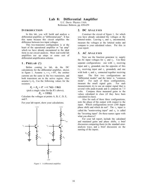
1. PRELAB (!)<br />
Before coming to lab, do the DC<br />
calculations for the differential amplifier, shown<br />
in figure 1. Assume v1 = v2 = 0V, the emitter<br />
currents are the same in the two transistors, and<br />
both transistors are in the active region. Also<br />
assume I C ≈I E . Use the following values for the<br />
resistors:<br />
RC = RB = R' = 47 . kΩ-10kΩ<br />
(pick a single value for the R’s above),<br />
R E<br />
= 100Ω.<br />
Calculate the voltages at points A, B, C, D, E,<br />
and F.<br />
For your lab report, show your calculations.<br />
R B<br />
A<br />
+15V<br />
C<br />
v 2<br />
R B<br />
B<br />
+15V<br />
F<br />
Q2<br />
D<br />
R C<br />
v out<br />
2. DC ANALYSIS<br />
Construct the circuit <strong>of</strong> figure 1, for which<br />
you have already calculated the voltages at the<br />
lettered nodes. Leaving v 1<br />
and v 2<br />
unconnected,<br />
measure the voltages at the lettered nodes and<br />
compare to your calculated values. Put this in<br />
your report.<br />
3. AC ANALYSIS<br />
Now use the function generator to supply<br />
the AC input voltages for v 1<br />
and v 2<br />
. Use three<br />
separate configurations: one with v 1<br />
receiving<br />
input and v 2<br />
grounded, one the opposite <strong>of</strong> this<br />
(v 2<br />
receiving input and v 1<br />
grounded), and one<br />
with both v 1<br />
and v 2<br />
connected together receiving<br />
input. The first two configurations are<br />
"differential modes" and the latter is "common<br />
mode". For each <strong>of</strong> these configurations,<br />
measure the small signal gain. For each<br />
measurement, try to use an output signal that is<br />
several volts peak-to-peak and is centered on 7.5<br />
volts. Compare these measured gains to the<br />
values calculated in class (if they have been<br />
calculated in class).<br />
Also for each <strong>of</strong> these three configurations,<br />
note the phase <strong>of</strong> the output with respect to the<br />
input. Which configurations invert (180 degree<br />
phase shift) and which do not? The v 1<br />
input is<br />
called the "noninverting input" and v 2<br />
is called<br />
the "inverting input". Do these names agree with<br />
what you observe?<br />
For your lab report, include the calculated<br />
and measured gains and phase shifts, a brief<br />
discussion comparing them (in the standard erroranalysis<br />
way), and a brief discussion on the<br />
naming <strong>of</strong> the inputs.<br />
v 1 Q1<br />
R'<br />
R E<br />
R E<br />
E<br />
-15V<br />
Figure 1: A differential amplifier.<br />
10
4. QUALITY OF OUTPUT<br />
Measure the output signal rise time. To do<br />
this, put a high frequency square wave on the<br />
noninverting input and ground the inverting<br />
input. Adjust the input voltage so the output is<br />
a fairly large amplitude. ("Large amplitude"<br />
means close to the power supply limits.) For<br />
your report, sketch the output and identify and<br />
measure the rise time.<br />
Ideally, an amplifier will be linear. That is,<br />
it will very accurately obey<br />
vout = Av<br />
vin + V<strong>of</strong>fset.<br />
(Compare to the equation for a line, y= mx+<br />
b<br />
from linear algebra.) Real amplifiers approach<br />
linearity only for a limited range <strong>of</strong> output<br />
voltages.<br />
Find the range <strong>of</strong> output voltages for which<br />
this amplifier is reasonably linear. To do this,<br />
put a large amplitude, medium frequency triangle<br />
wave on one <strong>of</strong> the inputs and ground the other.<br />
The output waveform will be very straight where<br />
the amplifier is linear and will appear curved<br />
where it is nonlinear. For your report, sketch a<br />
sample output waveform showing linear and<br />
nonlinear regions and mark the approximate<br />
voltage range where the output is linear.<br />
Last, increase the gain <strong>of</strong> the amplifier and<br />
see if this affects its linearity. To do this, short<br />
out the emitter resistors. Measure the gain (in<br />
noninverting differential mode only) <strong>of</strong> this new<br />
circuit and repeat the linearity check described<br />
above. R E<br />
provides negative feedback which<br />
should improve linearity and reduce gain. Is this<br />
what you observe? For your lab report, include<br />
the new measured gain, a new sketch <strong>of</strong> the<br />
output indicating nonlinearities, and a brief<br />
discussion <strong>of</strong> how R E<br />
affects linearity and gain.<br />
11
<strong>Physics</strong> 116A: <strong>Differential</strong> <strong>Amplifier</strong>:<br />
Analysis <strong>of</strong> Operation<br />
David E. Pellett<br />
<strong>UC</strong> <strong>Davis</strong> <strong>Physics</strong> <strong>Department</strong><br />
v. 1.0, 2/24/2000<br />
The differential amplifier shown in Fig. 1 is useful because:<br />
• it operates without input capacitors (DC amplifier);<br />
• it provides voltage gain for differential signals on the inputs, V d<br />
attenuating interfering common-mode signals, V c ≡ (V 1 + V 2 )/2;<br />
≡ V 1 − V 2 , while<br />
• it provides the inverting and non-inverting inputs needed for operational amplifiers.<br />
With slight variations, the circuit can also be made with pnp BJTs or FETs. A current<br />
source can replace R ′ and V EE for better common mode signal rejection.<br />
V CC<br />
V CC<br />
R C<br />
V 2<br />
V OUT<br />
R E<br />
V EE<br />
Typical Values:<br />
V CC = 15 V<br />
V EE = –15 V<br />
R C = 7.5 KΩ<br />
R E = 100 Ω<br />
I'<br />
V 1<br />
I 1 I 2<br />
V A<br />
R E<br />
R'<br />
Quiescent ("Q") Point:<br />
V 1 = V 2 = 0 V<br />
I 1 = I 2 = I 0 ≈ |V EE |/2R'<br />
V A ≈ –0.7 V – I 0 R E<br />
V OUT ≈ V CC – I 2 R C<br />
(assumes |V EE | >> 0.7 V<br />
R' = 7.5 KΩ<br />
and R' >> R E .)<br />
Figure 1: <strong>Differential</strong> amplifier circuit diagram with representative component values and Q<br />
point parameters for npn BJTs.<br />
The differential amplifier operation can be understood qualitatively as follows. V EE and<br />
R ′ form an approximate constant current source, I ′ ≈|V EE |/R ′ ,with<br />
I 1 + I 2 = I ′ .<br />
When both inputs are at 0 V, the current splits equally in the two branches.<br />
If V 1 is raised slightly while holding V 2 = 0, KVL going from input 1 to input 2 (ground)<br />
by way <strong>of</strong>point A tells us:<br />
V 1 − 0.7 V− I 1 R E + I 2 R E +0.7 V=0.<br />
1
This reduces to<br />
I 1 = I 2 + V 1 /R E .<br />
I 1 is now greater than I 2 ,soI 2 must have decreased since the total, I ′ , is approximately<br />
constant. Reducing I 2 lowers the voltage drop across R C ,soV out increases. V 1 is the noninverting<br />
input.<br />
In the same way, raising V 2 slightly with V 1 grounded increases I 2 . This now increases<br />
the voltage drop across R C and lowers V out . V 2 is the inverting input.<br />
A more complete analysis can be done using the small signal AC model for the circuit,<br />
shown in Fig. 2.<br />
R C<br />
v out<br />
v 1<br />
r e r e<br />
v 2<br />
i R 1 E R E<br />
v<br />
i 2 A<br />
αi 1 αi2<br />
α ≈ 1<br />
i'<br />
R'<br />
r e ≈ 26 Ω mA/I EQ<br />
Figure 2: Small signal AC model for the differential amplifier.<br />
Here, all voltages and currents have been replaced by the deviations from their values<br />
at the quiescient point. For example, i 1 = I 1 − I 0 . The transistors have been replaced by<br />
simple active region models.<br />
1. <strong>Differential</strong> mode gain:<br />
Define v d ≡ v 1 − v 2 . The differential mode gain is<br />
A vd ≡ v out /v d .<br />
Apply the following input voltages to the amplifier: v 1 = v d /2andv 2 = −v d /2. Use<br />
KVL:<br />
v 1 = i 1 (r e + R E )+(i 1 + i 2 )R ′ = v d /2,<br />
v 2 = i 2 (r e + R E )+(i 1 + i 2 )R ′ = −v d /2.<br />
Adding the equations and collecting terms results in i 2 = −i 1 , which also leads to<br />
v A =(i 1 + i 2 )R ′ =0. Therefore,<br />
i 2 = v 2 /(r e + R E )=−v d /2(r e + R E ).<br />
2
v out = −R C i 2 ,sov out = −R C (−v d )/2(r e + R E ). We can now solve for the differential<br />
mode gain:<br />
A vd ≡ v out /v d = R C /2(r e + R E ).<br />
2. Common mode gain:<br />
Define v c ≡ 1 (v 2 1 + v 2 ). The common mode gain is<br />
A vc ≡ v out /v c .<br />
Apply v 1 = v 2 = v c and use KVL to find i 2 in terms <strong>of</strong> v c = v 2 :<br />
v c = i 2 (r e + R E )+2i 2 R ′ ,<br />
Since v out = −i 2 R C ,<br />
i 2 = v c /(r e + R E +2R ′ ).<br />
A vc ≡ v out /v c = −R C /(r e + R E +2R ′ ).<br />
3