Lab 2: Op Amp Circuits - UC Davis
Lab 2: Op Amp Circuits - UC Davis
Lab 2: Op Amp Circuits - UC Davis

Create successful ePaper yourself
Turn your PDF publications into a flip-book with our unique Google optimized e-Paper software.
<strong>Lab</strong> 2: <strong>Op</strong> <strong>Amp</strong> <strong>Circuits</strong><br />
U.C. <strong>Davis</strong> Physics 116A<br />
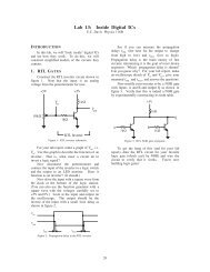
INTROD<strong>UC</strong>TION<br />
This lab introduces the operational amplifier<br />
or "op amp". The circuit is already constructed<br />
for you on a single IC (integrated circuit) and in<br />
this lab we will use the IC in several of its most<br />
popular configurations. For an introduction to<br />
op amps, see section 2.4 in Bobrow.<br />
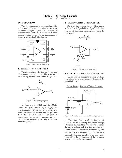
-input<br />
+input<br />
1<br />
2<br />
3<br />
offset<br />
null<br />
_<br />
+<br />
no<br />
connect<br />
+V cc<br />
8<br />
7<br />
6<br />
+15V<br />
output<br />
2. NONINVERTING AMPLIFIER<br />
Construct the noninverting amplifier shown<br />
in figure 3 with R 1<br />
= 1kΩ and R 2<br />
= 33kΩ. For<br />
your report, derive and experimentally verify the<br />
gain relation<br />
R R<br />
AV = 1<br />
+ 2<br />
.<br />
R<br />
V in +<br />
–<br />
R 2<br />
1<br />
V out<br />
-15V<br />
offset<br />
4 -Vcc<br />
null 5<br />
R 1<br />
Figure 1: Pinout for the 741 op amp.<br />
1. INVERTING AMPLIFIER<br />
The pinout diagram for the LM741 op amp<br />
IC is shown in figure 1. Use this to construct<br />
the inverting op amp circuit shown in figure 2.<br />
R 2<br />
Figure 3: The noninverting amplifier.<br />
3. CURRENT-TO-VOLTAGE CONVERTER<br />
An op amp can be used to produce a voltage<br />
proportional to a given current. Construct the<br />
circuit in figure 4.<br />
R 1<br />
_<br />
in<br />
v<br />
+<br />
out<br />
Current Source<br />
Current-to-Voltage Converter<br />
R 2<br />
= 100k Ω<br />
Figure 2: The inverting amplifier.<br />
At first, use R 1<br />
= 1kΩ and R 2<br />
= 33kΩ.<br />
Derive the gain formula AV =− R2 R1 and<br />
experimentally verify the gain for a 100Hz sine<br />
wave. Also calculate and measure the gain with<br />
R 2<br />
= 10kΩ and R 2<br />
= 100kΩ. For your lab<br />
report, give your derivation and compare the 2<br />
calculated and measured gains. Why is this called<br />
an inverting amp?<br />
+<br />
R 1<br />
= 1M Ω<br />
3-15V<br />
I in<br />
_<br />
+<br />
V out<br />
Figure 4: Current source with current-to-voltage converter.<br />
Verify that Vout<br />
=−Iin<br />
R2 for this circuit.<br />
(That is, do the following for several voltage<br />
settings on the variable power supply: Measure<br />
the supply voltage and from this calculate I in<br />
.<br />
Use the formula to calculate a theoretical V out<br />
and<br />
compare this to a measured V out<br />
. Include these<br />
measured values and calculations in your report<br />
along with a brief discussion of the agreement<br />
between theory and measurement.)<br />
4 4
Current Source<br />
~<br />
+15V<br />
I in<br />
Current-to-Voltage Converter<br />
R 2<br />
= 100k Ω<br />
_<br />
+<br />
V out<br />
Figure 5: Photodiode with current-to-voltage converter.<br />
Now replace the current source with a<br />
photodiode as shown in figure 5. Look at V out<br />
with the oscilloscope. For your lab report,<br />
measure the intensity of light (steady and<br />
oscillating) in the room.<br />
4. INTEGRATOR<br />
The name "operational amplifier" came from<br />
this amplifier's ability to perform mathematical<br />
operations. Two good examples of this are the<br />
integrator and differentiator which perform the<br />
operations of integration and differentiation,<br />
respectively. These are described in Bobrow in<br />
examples 3.7 and 3.4, respectively.<br />
10ΜΩ<br />
and describe what happens. Briefly discuss this<br />
in your report.<br />
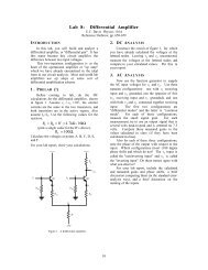
5. DIFFERENTIATOR<br />
Construct the differentiator circuit in figure<br />
7. Sketch the input and output waveforms for a<br />
1kHz sine wave, triangle wave, and square wave<br />
input as for the integrator. For your report,<br />
include your sketches and show that the output<br />
waveform is indeed the derivative of the input<br />
waveform.<br />
v in<br />
1k Ω<br />
0.01 µ F<br />
100 pF<br />
100 kΩ<br />
Figure 7: The differentiator amplifier circuit.<br />
_<br />
+<br />
v out<br />
Note here that the 100 pF capacitor (a very<br />
small value) is not in the ideal amplifier. Why<br />
do you think it is here? (Think about the<br />
derivative of a square wave, for example. Could<br />
high voltages damage a chip or put a significant<br />
noise into the circuit?) Briefly discuss this in<br />
your report.<br />
v in<br />
100k Ω<br />
_<br />
0.01 µ F<br />
+<br />
v out<br />
Figure 6: The op amp integrator circuit.<br />
Construct the integrator shown in figure 6.<br />
Sketch the input and output waveforms for 1kHz<br />
sine wave, triangle wave, and square wave inputs.<br />
Try to guess what each waveform will look like<br />
ahead of time. For your report, include your<br />
sketches and show that the output waveform is<br />
indeed the integral of the input waveform.<br />
Note that the 10MΩ resistor (a very large<br />
value) is not in the ideal integrator circuit. What<br />
is it there for? (Think about what would happen<br />
if a small DC component was present in the<br />
input waveform. What would integrating this<br />
constant do after a short time?) Try removing it<br />
5 5