Bi-Directional Isolated DC-DC Converter for Next-Generation Power ...
Bi-Directional Isolated DC-DC Converter for Next-Generation Power ...
Bi-Directional Isolated DC-DC Converter for Next-Generation Power ...

You also want an ePaper? Increase the reach of your titles
YUMPU automatically turns print PDFs into web optimized ePapers that Google loves.
<strong>Bi</strong>-<strong>Directional</strong> <strong>Isolated</strong> <strong>DC</strong>-<strong>DC</strong> <strong>Converter</strong> <strong>for</strong> <strong>Next</strong>-<strong>Generation</strong><br />
<strong>Power</strong> Distribution - Comparison of <strong>Converter</strong>s using<br />
Si and SiC Devices<br />
D. Aggeler*, J. <strong>Bi</strong>ela*, S. Inoue**, H. Akagi**, J. W. Kolar*<br />
* ETH Zurich, <strong>Power</strong> Electronic Systems Laboratory, Switzerland<br />
** Tokyo Institute of Technology, Department of Electrical and Electronic Engineering, Japan<br />
Abstract— In this paper two bi-directional <strong>DC</strong>-<strong>DC</strong> converters<br />
<strong>for</strong> a 1MW next-generation BTB system of a distribution system,<br />
as it is applied in Japan, are presented and compared with<br />
respect to design, efficiency and power density. One <strong>DC</strong>-<strong>DC</strong><br />
converter applies commercially available Si-devices and the other<br />
one high voltage SiC switch, which consists of a SiC JFET cascode<br />
(MOSFET+1 JFET) in series with five SiC JFETs.<br />
In the comparison also the high frequency, high voltage<br />
trans<strong>for</strong>mer, which ensures galvanic isolation and which is a<br />
core element of the <strong>DC</strong>-<strong>DC</strong> converter, is examined in detail by<br />
analytic calculations and FEM simulations.<br />
For validating the analytical considerations a 20kW SiC <strong>DC</strong>-<br />
<strong>DC</strong> converter has been designed in detail. Measurement results<br />
<strong>for</strong> the switching and conduction losses have been acquired from<br />
the SiC and also <strong>for</strong> a Si system <strong>for</strong> calculating the losses of the<br />
scaled 1MW system.<br />
Keywords – <strong>Next</strong>-generation BTB system, High voltage<br />
HF <strong>DC</strong>-<strong>DC</strong> converter, SiC JFET cascode, High voltage HF<br />
trans<strong>for</strong>mer<br />
I. INTRODUCTION<br />
Generally, the power generation with renewable energy<br />
sources is a discontinuous process and in most of the cases<br />
depending on the environment. Feeding in the produced<br />
energy into a distribution system influences the overall energy<br />
flow. There<strong>for</strong>e, it is a challenge to control and keep the<br />
energy stabilized. Figure 1 shows a Japanese 6.6kV power<br />
distribution system having two feeders from a trans<strong>for</strong>mer.<br />
Today, each distribution system in Japan has radial feeders,<br />
<strong>for</strong>ming no loop. If the distributed power generators are<br />
installed concentrated on one of the feeders (feeder 2 in figure<br />
1), regulating voltage on both feeders within an acceptable<br />
range becomes difficult.<br />
Back-to-Back (BTB) systems, also known as loop controllers,<br />
have been investigated to solve the problem of power<br />
flow balancing. The dotted lines in figure 1 show where<br />
the BTB system would be installed and in figure 2 a circuit<br />
configuration is shown which is presented in [1]. The linefrequency<br />
(50Hz or 60Hz) trans<strong>for</strong>mers in figure 2 play an<br />
important role in stepping down/up the voltage and in ensuring<br />
Distribution<br />
Trans<strong>for</strong>mer<br />
6.6kV Feeder 1<br />
6.6kV Feeder 2<br />
BTB<br />
System<br />
Distributed<br />
<strong>Power</strong><br />
Generators<br />
Fig. 1: A 6.6kV distribution system in Japan having two feeders.<br />
50/60Hz<br />
Trans<strong>for</strong>mer<br />
6.6kV<br />
Feeder 1<br />
Two- or Three-Level <strong>Converter</strong><br />
50/60Hz<br />
Trans<strong>for</strong>mer<br />
6.6kV<br />
Feeder 2<br />
Fig. 2: The present BTB system <strong>for</strong> the 6.6kV power distribution<br />
system.<br />
galvanic isolation between the two feeders. Especially, galvanic<br />
isolation is desirable to prevent a zero-sequence current<br />
circulating between the two feeders. However, one 6.6kV,<br />
1MW trans<strong>for</strong>mer weighs approximately 3,000kg to 4,000kg,<br />
and may be too heavy to be mounted on an electric pole.<br />
Actually, the solution with the trans<strong>for</strong>mers results in a large<br />
volume and occupy a big part of the conversion system.<br />
Furthermore, the costs are quite high due to rising prices <strong>for</strong><br />
raw materials. As a consequence, a new topology is under<br />
investigation substituting the two line-frequency trans<strong>for</strong>mers.<br />
The present BTB system with two three-phase, line frequency<br />
trans<strong>for</strong>mers will be replaced by the next-generation BTB<br />
system given in figure 3. There it is shown, that a BTB system<br />
in the next-generation consists of a number of converter cells<br />
which in each case consists of a rectifier/inverter stage and a<br />
<strong>DC</strong>-<strong>DC</strong> converter. The galvanic isolation of the proposed BTB<br />
system is guaranteed by a high frequency (HF) trans<strong>for</strong>mer.<br />
Due to the high operating frequency the volume and the weight<br />
of the passive components is reduced very much compared to<br />
the line-frequency trans<strong>for</strong>mers.<br />
For the design of the full bridge converter different device<br />
technologies can be used: on the one hand a realization<br />
with Si IGBT devices [2] and on the other hand with SiC<br />
JFET components provided by SiCED [3]. In the following<br />
a galvanic isolated BTB system with SiC will be designed,<br />
according the specification parameters given in table I and<br />
compared with the Si system of [2].<br />
In section II the operation principle of the next-generation<br />
BTB system solution is summarized shortly. The following<br />
section III focuses on the <strong>DC</strong>-<strong>DC</strong> converter with SiC JFET<br />
cascodes. There, the converter specifications, the dual active<br />
bridge (DAB) as well as the high voltage (HV) SiC switch<br />
are explained. In section IV experimental results of the SiC<br />
Input voltage 6.6kV<br />
Output voltage 6.6kV<br />
Rated <strong>Power</strong> 1MW<br />
Current THD 5%<br />
Each harmonic
First <strong>Converter</strong> Cell<br />
6.6kV<br />
Circuit<br />
in<br />
figures<br />
4, 5<br />
6.6kV<br />
V D1<br />
Bridge 1 Bridge 2<br />
C snub P <strong>DC</strong><br />
L a /2 L a /2<br />
v 1 i 1<br />
v 2<br />
1 : 1<br />
10kHz<br />
V D2<br />
Second <strong>Converter</strong> Cell<br />
Fig. 4: A bi-directional isolated <strong>DC</strong>-<strong>DC</strong> converter.<br />
N-th <strong>Converter</strong> Cell<br />
Fig. 3: A 6.6kV BTB system in the next generation.<br />
JFET cascode and the design of the HV-HF trans<strong>for</strong>mer based<br />
on analytic calculations and FEM simulations are presented.<br />
Furthermore, a 3D-model of the proposed <strong>DC</strong>-<strong>DC</strong> converter is<br />
shown. Section V summarizes the per<strong>for</strong>mance of the Si IGBT<br />
system presented in [2]. Thereafter, the possible solutions <strong>for</strong> a<br />
next-generation BTB system – Si IGBT and SiC JFET cascode<br />
– are compared <strong>for</strong> a 1MW system in section VI. In section<br />
VII another application of the high voltage SiC cascode – a<br />
medium voltage motor drive – is shortly presented and finally<br />
conclusions are drawn in section VIII.<br />
II. NEXT-GENERATION MEDIUM VOLTAGE BTB SYSTEM<br />
The next-generation BTB system (figure 3) consists of a<br />
rectifier/inverter stage and as the core circuit a bi-directional,<br />
galvanic isolated <strong>DC</strong>-<strong>DC</strong> converter, as shown in figure 4 (Si<br />
IGBT) or figure 5 (SiC JFET cascode), is applied.<br />
The cascaded converter cells <strong>for</strong>m a single-phase part of the<br />
BTB system where each converter cell consists of a <strong>DC</strong>-<strong>DC</strong><br />
converter. The <strong>DC</strong>-link voltage in each converter cell depends<br />
on the number of cascade connections N. Hence, wave<strong>for</strong>m<br />
levels, AC input voltages and <strong>DC</strong>-link voltages per converter<br />
cell are calculated, <strong>for</strong> a different number N of converter cells,<br />
and summarized in table II.<br />
The analyzed Si IGBT system consists of six converter cells<br />
in each phase (N=6), what results in a <strong>DC</strong>-link voltage of<br />
1.02kV in each cell, allowing to use 1.7kV IGBTs available<br />
at a lower cost than higher voltage Si devices. The application<br />
of several converter cells and phase shifted unipolar sinusoidal<br />
PWM of the rectifier/inverter stage, where the triangular<br />
carrier signal in one converter cell is phase shifted by π/N<br />
from each other, results in a multilevel wave<strong>for</strong>m of the<br />
line-to-neutral voltage. There<strong>for</strong>e, the equivalent switching<br />
frequency is 2Nf c , where f c is the carrier frequency. As<br />
N Wave<strong>for</strong>m AC Input <strong>DC</strong> Link<br />
1 3 Level 3,811V 6.10kV<br />
2 5 Level 1,905V 3.48kV<br />
3 7 Level 1,270V 2.03kV<br />
4 9 Level 952V 1.52kV<br />
5 11 Level 752V 1.22kV<br />
6 13 Level 635V 1.02kV<br />
7 15 Level 544V 870V<br />
8 17 Level 476V 762V<br />
9 19 Level 423V 677V<br />
TABLE II: Voltage and wave<strong>for</strong>m levels depending on the number<br />
N of converter cells of a next-generation BTB system.<br />
V 1<br />
6.1kV<br />
C <strong>DC</strong>,1<br />
T 11 T 12 T 21 T 22<br />
1:1<br />
i L L<br />
v T1 v T2<br />
D<br />
50kHz<br />
T 14 T 13 T 24 T 23<br />
G<br />
S<br />
cf. Figure 6<br />
C <strong>DC</strong>,2<br />
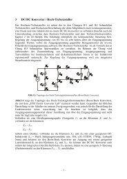
Fig. 5: SiC high voltage <strong>DC</strong>-<strong>DC</strong> converter.<br />
V 2<br />
6.1kV<br />
a result, the voltage wave<strong>for</strong>m has (2N+1) levels with the<br />
switching frequency of 2Nf c . Thus, the carrier frequency of<br />
the PWM converters can be as low as 4kHz by six converter<br />
cells in each phase.<br />
The application of SiC JFET cascode devices <strong>for</strong> the <strong>DC</strong>-<br />
<strong>DC</strong> converter offer a HV blocking capability and thus only<br />
one converter cell (N=1) is required. Accordingly, a smaller<br />
number of power devices is utilized. While in the Si IGBT<br />
based design (N=6) the number of power devices is 288, <strong>for</strong><br />
the SiC JFET cascode system 48 semiconductor devices are<br />
used. Due to the lower number of converter cells, in the SiC<br />
system a higher carrier frequency is needed.<br />
III. OPERATION PRINCIPLE SIC HV-HF-CONVERTER<br />
The proposed HV and HF DAB converter with SiC JFET<br />
cascode, replacing the conventional BTB system with the two<br />
line-frequency trans<strong>for</strong>mers, is shown in figure 5.<br />
The specification of the SiC DAB converter is given in<br />
table III. The design requirements <strong>for</strong> the distribution system<br />
given at a line-to-line voltage V AC of 6.6kV (table I), a<br />
<strong>DC</strong>-link voltage V <strong>DC</strong> of 6.1kV (with 13% safety margin,<br />
table II) is resulting. One goal of the next-generation BTB<br />
system is reduction in terms of size, especially of the passive<br />
components. A high switching frequency will result in smaller<br />
magnetic components/trans<strong>for</strong>mer but the HF losses increase<br />
considerable. For that reason the switching frequency of<br />
50kHz is chosen to limit HF losses. Consideration of power<br />
controllability and a dynamical margin of continuous current<br />
flowing a rated power of 20kW is designed <strong>for</strong> the DAB. For<br />
transferring a bigger amount of power, devices must be connected<br />
in parallel to increase the continuous current capability.<br />
Furthermore, the trans<strong>for</strong>mer turns ratio is fixed because of the<br />
equal voltage level on both side of the distribution system.<br />
<strong>DC</strong>-link Voltage<br />
6.1kV<br />
Switching frequency 50kHz<br />
Rated <strong>Power</strong><br />
20kW<br />
Trans<strong>for</strong>mer turns ratio 1:1<br />
Peak inductance current 7A<br />
<strong>DC</strong>-link voltage ripple < 5%<br />
TABLE III: Specification of <strong>DC</strong>-<strong>DC</strong> converter.
A. Dual Active Bridge<br />
As modulation method the common phase shift operation<br />
is chosen <strong>for</strong> the DAB. The low computation complexity of<br />
the phase shift method, the simplicity of the circuit and the<br />
reduced power losses due to zero voltage switching (ZVS)<br />
are the main reasons <strong>for</strong> the wide application of this method.<br />
Characteristic of the DAB principle is the power transfer from<br />
the active bridge on the input side via the galvanic isolation<br />
(trans<strong>for</strong>mer) to the active bridge on the output side. There,<br />
the amount of transferred power is controlled by the phase<br />
shift angle φ [4],<br />
P = V 1V 2 /n · φ · (π − φ)<br />
2π 2 f S L<br />
and the leakage inductance is used as energy storing element.<br />
The transferred power depends nonlinearly on the phase shift<br />
angle and is limited by the switching frequency and the<br />
leakage inductance. The minimal phase shift angle and with<br />
this the minimal controllable power step is given by the clock<br />
frequency of the control board. Depending on the nonlinear<br />
relation of power and phase shift angle, the biggest gradient<br />
is with a phase shift angle of zero degree. There the maximal<br />
power step will appear respective the minimal controllable<br />
power at this point. With an increased phase shift angle, the<br />
power step will decrease and the controllable power will be<br />
smaller.<br />
In [5] the active and reactive power are shown as a function<br />
of the phase shift angle. A high phase shift value will increase<br />
significantly the reactive part of the power and only a little bit<br />
the active power. Consequently, the efficiency of the converter<br />
is reduced. A small phase shift angle the control signal<br />
constrain the controllability of the power steps. There<strong>for</strong>e,<br />
an operation in the phase shift interval of [ π 4 , π 3<br />
] is favorable<br />
and chosen <strong>for</strong> the considered DAB.<br />
In order to verify the operation of the DAB topology a<br />
simulation model was built <strong>for</strong> the specification given in table<br />
III. There, only a simplified equivalent circuit of the HV SiC<br />
switch was used. An exact model, which describes static<br />
and dynamic behavior of the HV switch in more detail is<br />
under investigation. Figure 6 shows the simulated trans<strong>for</strong>mer<br />
voltages v T 1 and v T 2 with the inductor current i L , whereas<br />
the stray capacitance of the trans<strong>for</strong>mer is considered.<br />
B. High voltage SiC switch<br />
As a result of the operation voltage, switches with a HV<br />
blocking capability are required. Thus, SiC JFET cascode are<br />
chosen because of the good material characteristics of SiC,<br />
as the low on-state losses and high frequency operation. Two<br />
different modules are applied: one contains four SiC JFETs,<br />
two connected in series and two in parallel. For controlling the<br />
switch additionally a low-voltage Si MOSFET is connected to<br />
the lower JFETs (A, figure 7). In the other module just two<br />
SiC JFETs are connected in series and two in parallel (B,<br />
figure 7).<br />
The structure of the SiC JFET die is designed with a internal<br />
pn-junction from source to drain [6], which is working as<br />
the freewheeling diode of the SiC JFET. Thus, no external<br />
freewheeling diodes are required.<br />
The gates of the JFETs are connected to additional diodes<br />
<strong>for</strong> passive controlling the turn-on and turn-off mechanism of<br />
(1)<br />
Voltage [ kV ]<br />
8<br />
4 i L V T2<br />
0<br />
-4<br />
-8<br />
V T1<br />
0 10 20 30 40<br />
Time [ us ]<br />
Fig. 6: Simulated wave<strong>for</strong>ms <strong>for</strong> the phase shift mode at<br />
V 1=V 2=6.1kV and P Out = 20kW (f s=50kHz, φ = π/3).<br />
each JFET. This diode is a low leakage fast recovery epitaxial<br />
diode (FRED) and is included in the SEMITOP package.<br />
In order to achieve the required blocking voltage <strong>for</strong> the<br />
<strong>DC</strong>-link input voltage, multiple modules must be connected<br />
in series. The conventional JFET is a normally-on device.<br />
For this reason a low-voltage Si MOSFET is connected in<br />
series which is a normally-off device and controllable with a<br />
standard gate drive circuit. Both modules are mounted in a<br />
SEMITOP package (figure 7) by Semikron International [7].<br />
The ratings of the JFET are a blocking voltage V CES of 1500V<br />
and a continuous drain current I D of 8A.<br />
The basic concept of the SiC JFET cascode switch is<br />
described in [8]. There, also the static blocking characteristics<br />
and the dynamic switching behavior are discussed. In the<br />
on-state of the SiC JFET cascode, a positive gate voltage is<br />
applied to the MOSFET. Then, the gate of the lower JFET in<br />
the A module is connected to the source of the MOSFET and<br />
the JFET is conducting. Also the other in series connected<br />
JFETs are conducting due to its already mentioned normallyon<br />
characteristics. For this case the JFETs work as a resistor<br />
connected in series to the on-resistance of the MOSFET.<br />
In the blocking state the MOSFET gate is shorted to the<br />
ground and the drain-source voltage of the MOSFET increases<br />
until the pinch-off voltage of the first JFET is reached. Further<br />
increasing of the MOSFET’s drain-source voltage is now<br />
blocked by the first JFET, which is blocking the excess voltage,<br />
until the belonging Diode between the gate of the upper and<br />
the lower JFET reaches its avalanche blocking voltage. At<br />
this point the avalanche current is flowing and the gate of the<br />
second JFET drops down below its source potential. The gatesource<br />
voltage of the second JFET is negative and there<strong>for</strong>e<br />
in blocking state. For the next stages this process is iterative<br />
B<br />
A<br />
G<br />
S<br />
D<br />
B<br />
B<br />
A<br />
8<br />
4<br />
0<br />
-4<br />
-8<br />
Current [ A ]<br />
Fig. 7: SiC JFET cascode mounted in a SEMITOP package.
until the <strong>DC</strong>-link voltage is blocked.<br />
IV. DESIGN OF <strong>DC</strong>-<strong>DC</strong> CONVERTER<br />
In the following the design of the SiC <strong>DC</strong>-<strong>DC</strong> converter<br />
<strong>for</strong> an output power of 20kW is presented. For calculating<br />
the switching and conduction losses measurement results <strong>for</strong><br />
the SiC JFET are presented. Moreover, the design of the high<br />
voltage trans<strong>for</strong>mer will be discussed in detail and a 3D model<br />
of the converter is presented.<br />
A. Experimental Results<br />
For an application in the distribution system with the<br />
specifications given in table I the HV switch consists of two<br />
modules B and one module A, resulting in a total blocking<br />
voltage of 9kV. There, a safety voltage margin is included <strong>for</strong><br />
dynamic voltage balancing. In the following these three series<br />
connected modules are denoted as one HV switch.<br />
For determining the switching and conducting losses an<br />
experimental setup as shown in figure 8 was built. There,<br />
also a simplified schematic is given. On the high voltage side<br />
the gate of the HV switch is connected to the source so that<br />
it works as freewheeling diode. The HV switch on the low<br />
voltage side is actively controlled by a gate driver.<br />
In a first step single pulses <strong>for</strong> testing the turn-off behavior<br />
with an inductive load at different current amplitudes have<br />
been acquired. With the measured current and voltage wave<strong>for</strong>ms<br />
the ZVS turn-off losses of the DAB converter can be<br />
calculated. In a next step double pulse measurements will be<br />
per<strong>for</strong>med in order to test also the turn-on behavior of the SiC<br />
JFET devices.<br />
The gate drive circuit is designed with a small trans<strong>for</strong>mer,<br />
which could withstand the 6.1kV <strong>DC</strong>-link voltage, <strong>for</strong> the<br />
gate drive power supply. Furthermore, the gate drive signal is<br />
transferred via fiber optic to the gate driver, where the standard<br />
MOSFET driver IXDI409SI from IXYS is used. The gatesource<br />
voltage to turn the HV switch on is +12V. For turning<br />
the MOSFET off a negative gate-source voltage of -5V is used<br />
in order to reduced the influence of induced noise.<br />
In the test circuit (figure 8) the HV switch is on the bottom<br />
side of the PCB between the film capacitors mounted on a heat<br />
sink behind the fan. Additionally, to the film capacitances<br />
ceramic capacitors are placed on the top side close to the<br />
switches in order to minimize the stray inductance and reduce<br />
voltage overshoot.<br />
In figure 9 and figure 10 experimental results <strong>for</strong> the<br />
switching behavior with a <strong>DC</strong>-link voltage of 1.6kV and a<br />
46mm<br />
100mm<br />
Fan<br />
103mm<br />
22mm<br />
Gate drive<br />
Ceramic<br />
capacitors<br />
215mm<br />
Film<br />
capacitors<br />
Gate<br />
Signal<br />
+Vdc<br />
cf. Figure 6<br />
Fig. 8: <strong>Power</strong> loss measurement setup <strong>for</strong> the HV switch with the<br />
corresponding simplified schematic.<br />
L<br />
gate resistance of 10Ω are presented. The measurements are<br />
made with high voltage differential probes from Tektronix and<br />
trimmed high voltage current trans<strong>for</strong>mers.<br />
The turn-on current wave<strong>for</strong>m in figure 9 of the HV switch<br />
shows a significant peak of capacitive current during the<br />
falling edge of the voltage. This usually would result in<br />
significant turn-on losses of the SiC JFET. In the DAB,<br />
however, the switch is operated under ZVS conditions what<br />
leads to negligible turn-on losses.<br />
In figure 10 the turn-off characteristic is shown. There,<br />
the current first decreases rapidly to half of the original drain<br />
current, stays constant and then falls down to zero. The total<br />
fall time of the current is approximately 80ns. The drainsource<br />
voltage V <strong>DC</strong> rises within 60ns. This current shape<br />
reflects a capacitive turn-off behavior as shown by the dashed<br />
line in figure 10.<br />
The equivalent circuit during the capacitive turn of is shown<br />
in figure 11. During the period (A) the load current flows<br />
through the low side HV switch. At turn-off, the current<br />
splits up into two capacitive currents (B). One is charging<br />
the lower capacitance which has a high value at low drainsource<br />
voltage. With increasing voltage the capacitance is<br />
decreasing due to the spreading space charge region. The<br />
second current is discharging the capacitance of the upper<br />
switch, which is increasing with increasing voltage. Finally,<br />
the load current flows through the freewheeling diode of the<br />
upper HV switch (C) and then in reverse direction through<br />
the n-channel as soon as the upper switch is turned-on. Due<br />
to this approximately capacitive turn-off behavior (ZVS) the<br />
turn-off switching losses are negligible.<br />
There, the interlocking delay time must be larger than the<br />
rise time of the drain-source voltage in order to guarantee soft<br />
Voltage [V]<br />
1800<br />
1200<br />
600<br />
0<br />
Voltage<br />
Capacitive<br />
peak current<br />
Current<br />
0 40 80 120 160 200<br />
Time [ns]<br />
Fig. 9: Turn-on characteristic of the SiC HV switch: drain-source<br />
voltage and drain-source current.<br />
Voltage [V]<br />
1800<br />
1200<br />
600<br />
0<br />
Current<br />
Voltage<br />
Approximated<br />
capacitive<br />
current<br />
0 40 80 120 160 200<br />
Time [ns]<br />
Fig. 10: Turn-off characteristic of the SiC HV switch: drain-source<br />
voltage and drain-source current with approximated capacitive<br />
current flow (dashed).<br />
9<br />
6<br />
3<br />
0<br />
3<br />
9<br />
6<br />
0<br />
Current [A]<br />
Current [A]
+Vdc<br />
+Vdc<br />
+Vdc<br />
SiC JFETs<br />
cf. Figure 6<br />
Fan<br />
Current<br />
measurement<br />
L<br />
L<br />
L<br />
Diode<br />
MOSFET<br />
cf. Figure 6<br />
A B C<br />
Fig. 11: Current flow during turn-off: A) HV switch is in on-state.<br />
B) Charge/discharge of capacitors. C) High side diode is<br />
conducting.<br />
switching. In the considered case with a voltage of 1.6kV a<br />
interlocking time of minimal 80ns results. For a constant load<br />
current this time will increase with higher <strong>DC</strong>-link voltages.<br />
In figure 12 the drain-source voltages <strong>for</strong> different <strong>DC</strong>link<br />
voltages are shown at turn-off. There, the on time of<br />
the HV switch and the load was the same <strong>for</strong> all <strong>DC</strong>-link<br />
voltages. This results in different turn-off current amplitudes<br />
and decreasing rise times of the HV switch voltage. At a <strong>DC</strong>link<br />
voltage of 1.6kV the du/dt is approximately 24kV/µs.<br />
During the switching tests several external diodes (FRED)<br />
have been destroyed. This probably results from excessive<br />
avalanche energies during the turn-off of the JFETs at rising<br />
voltages. Due to these effects it was not possible to measure<br />
the switching behavior at higher voltages than 1.6kV. In a next<br />
step the external diodes will be replaced by higher avalanche<br />
energy rated ones and the HV SiC switch will be built up<br />
with discrete components in order to be able to measure all<br />
relevant signals. With the discrete SiC JFET cascode as shown<br />
in figure 13 the switching behavior at higher voltages will be<br />
investigated and presented in a future paper.<br />
Besides the switching losses also the conduction losses are<br />
required <strong>for</strong> calculating the overall system losses. There<strong>for</strong>e,<br />
the on-resistance R DS,on of the HV switch has been measured.<br />
The value is approximately 1.35Ω at 25 ◦ C, which results in<br />
18.7W conduction losses in <strong>for</strong>ward direction per HV switch<br />
at 50kHz and a continuous load current of 4A. For higher<br />
temperatures this value must be multiplied by (T j /298) 1.6 ,<br />
where T j is the absolute junction temperature.<br />
In the reverse direction the current first flows through the<br />
antiparallel diodes of the MOSFET and of the JFETs. The<br />
Voltage [V]<br />
1800<br />
1200<br />
600<br />
0<br />
1.6kV<br />
1.5kV<br />
1.3kV<br />
1.11kV<br />
1kV<br />
0 40 80 120 160 200<br />
Time [ns]<br />
Fig. 12: HV SiC switch turn-off behavior of different <strong>DC</strong>-link voltages,<br />
R Gate = 10Ω.<br />
Heat sink<br />
Fig. 13: HV SiC switch built with discrete components.<br />
<strong>for</strong>ward voltage of the intrinsic antiparallel JFET diodes is<br />
in the range of 4V at a current of 4A. This would lead<br />
to relatively large conduction losses during the freewheeling<br />
period. However, as soon as the MOSFET and the JFETs<br />
are turned on the current could also flow in reverse direction<br />
through the n-channel of the MOSFET/JFETs which has a<br />
resistance in the range of 1.35Ω what results in much lower<br />
reverse conduction losses. These are 3.7W per HV switch <strong>for</strong><br />
conducting MOSFET/JFETs and 0.39W <strong>for</strong> the short period<br />
where the freewheeling diodes are conducting.<br />
B. High Voltage - High Frequency Trans<strong>for</strong>mer<br />
In the next-generation BTB system the line-frequency trans<strong>for</strong>mer<br />
should be replaced by a HV trans<strong>for</strong>mer operating<br />
at HF. Each <strong>DC</strong>-<strong>DC</strong> converter in the BTB system uses one<br />
trans<strong>for</strong>mer which also ensures the galvanic isolation between<br />
the input and output stage. The HV-HF trans<strong>for</strong>mer is one of<br />
the core elements in DAB operation considering power transfer<br />
and efficiency of the whole <strong>DC</strong>-<strong>DC</strong> converter. The phase shift<br />
operation mode of the DAB defines the requirements of the<br />
trans<strong>for</strong>mer, which will be designed in the following <strong>for</strong> an<br />
output power of 20kW and a phase shift angle between π 4 and<br />
π<br />
3<br />
. Due to the HF operation ferrite material must be used <strong>for</strong><br />
the core and the HF losses in the windings must be considered.<br />
For calculating the core losses Van den Bossche’s [9] loss<br />
model of ferrites cores, considering non-sinusoidal wave<strong>for</strong>ms,<br />
is used and compared to the losses resulting with the conventional<br />
Steinmetz equation and with also the modified Steinmetz<br />
equation [10]. The values of the loss models do not differ<br />
significantly and <strong>for</strong> the considered design the worst case value<br />
is used.<br />
Based on these equations different ferrite materials have<br />
been examined. There, it turned out that the N87 material from<br />
Epcos has the lowest core losses at the specified switching<br />
frequency of 50kHz and a maximal flux density of 150mT.<br />
The core selection results in four UU93/152/30 cores, where<br />
the primary and secondary winding are wounded around the<br />
middle leg as shown in the 3D-Model (figure 16) of the 20kW<br />
<strong>DC</strong>-<strong>DC</strong> converter system. For choosing the number of turns<br />
and also the flux density in the core different designs have<br />
been compared. There, it turned out that with 120 turns on<br />
the primary and on the secondary winding the lowest overall<br />
losses occur. In this operating point also the core and the HF<br />
losses in the windings are approximately balanced.<br />
For guaranteeing a high isolation voltage the distance between<br />
the windings and also between the winding and the<br />
core must be large enough and some high voltage isolating<br />
material must be used <strong>for</strong> the bobbin. Furthermore, the<br />
winding should be covered by an isolating material at the<br />
outer side between the winding and the core. The insulation
of the wire itself must be capable of withstanding at least<br />
voltage between the different layers of the winding. These<br />
requirements significantly influence the winding arrangement<br />
of the trans<strong>for</strong>mer. In figure 14 a possible arrangement, which<br />
fulfils the above mentioned requirements, is shown.<br />
There, each winding is distributed into three chambers in<br />
order to reduce the layer voltage and the parasitic capacitance<br />
of the trans<strong>for</strong>mer [11]. This results in a relatively low layer<br />
voltage, what is important <strong>for</strong> the high frequency operation<br />
with high du/dt-values. The fast edges of the voltage leads<br />
to a non uni<strong>for</strong>m voltage distribution between the single turns<br />
of one winding and to higher turn voltages at the ends of<br />
the winding during high du/dt. This is like charging a<br />
transmission line with a voltage pulse where a wave travels<br />
along the line until a uni<strong>for</strong>m distribution is reached. This<br />
effect will be examined in detail in a future paper.<br />
Another advantage of the higher number of chambers is an<br />
interleaving of the windings which could be used <strong>for</strong> reducing<br />
the HF losses in the windings or to control the leakage<br />
inductance of the trans<strong>for</strong>mer. In the considered case the two<br />
inner chambers are interleaved, i.e. primary and secondary<br />
chamber are exchanged and a sequence: primary - primary -<br />
secondary - primary - secondary - secondary chamber results<br />
(cf. figure 14). The two chambers in the middle of the winding<br />
window have less turns than the outer ones. Instead of 9 layers<br />
and 5 turns per layer, only 6 layers and 5 turns. With this<br />
arrangement a leakage inductance of approximately 4mH –<br />
calculated by 3D FEM simulations with MAXWELL T M (cf.<br />
figure 15)– results. This inductance is required <strong>for</strong> transferring<br />
the rated power of 20kW at the optimal phase shift angle of<br />
π/3. Thus, no additional external inductor is needed and the<br />
power density of the system increases.<br />
In conventional windings the layers are wound from the left<br />
to the right and then back in the next layer (S- or U-winding).<br />
There, the maximum voltage between two consecutive layers<br />
is twice the layer voltage – in the considered case maximal<br />
500V . This relatively high layer-to-layer voltage could be<br />
divided by two with a Z-winding, where each layer is wound<br />
in the same direction, i.e. <strong>for</strong> example all layers are wound<br />
from left to right. In this case the wire must be returned to<br />
the beginning of the layer outside the chamber in order to<br />
avoid a crossing of all wires of the considered layer. In order<br />
to guarantee a high isolating voltage also <strong>for</strong> the returning<br />
wire also the middle leg of the core is surrounded by an<br />
insulation. In table IV the trans<strong>for</strong>mer design characteristics<br />
are summarized.<br />
For reducing the influence of skin- and proximity effects<br />
litz wire with 315 strands / strand diameter of 0.071mm, a<br />
total external diameter of 2.01mm and 1.27mm 2 cross section<br />
is used.<br />
35mm<br />
P<br />
1mm<br />
P<br />
96mm<br />
2mm 8mm<br />
S P S S<br />
Core<br />
Fig. 14: Arrangement of the trans<strong>for</strong>mer windings.<br />
P P<br />
Insulation<br />
S<br />
Core<br />
P<br />
S S<br />
Interleaved<br />
winding<br />
Fig. 15: Energy density in a cut plane through the core determined<br />
by a 3D FEM simulation with Maxwell T M of the specified<br />
trans<strong>for</strong>mer as shown in figure 14.<br />
Material<br />
N87<br />
Turn number 120<br />
Turn ratio 1:1<br />
Transferred power 20kW<br />
Core losses (25 ◦ C) 35W<br />
(100 ◦ C) 15W<br />
HF losses (25 ◦ C) 24W<br />
(100 ◦ C) 30W<br />
Leakage inductance 3.4mH<br />
Main inductance 215mH<br />
Magnetizing current 283mA<br />
Specified max. flux density 150mT<br />
Effective cross section 3360mm 2<br />
Effective volume 1188cm 3<br />
TABLE IV: Characterization of the HV-HF trans<strong>for</strong>mer.<br />
C. Rectifier/Inverter<br />
Besides the <strong>DC</strong>-<strong>DC</strong> converter also single phase PWM<br />
converters in the input (rectifier) and output (inverter) stage<br />
of the BTB system are required. There, also the HV SiC<br />
cascodes is applied as switching device in order to reduce the<br />
switching losses and the number of series connected stages.<br />
The selection of the switching frequency is a trade-off between<br />
switching/HF-/capacitor losses and the size of the input/output<br />
inductance. With the relatively low switching losses of the SiC<br />
cascode a switching frequency of 50kHz is achievable what<br />
results in small passive components.<br />
The required capacitance <strong>for</strong> a voltage ripple v <strong>DC</strong>,link,pp of<br />
less than 5% of the <strong>DC</strong>-link voltage V <strong>DC</strong>,link can be calculated<br />
[12] by<br />
C <strong>DC</strong>,min =<br />
P<br />
V <strong>DC</strong>,link · ω · v <strong>DC</strong>,link,pp<br />
, (2)<br />
where P is the nominal power and ω is the line-frequency. For<br />
dimensioning the input/output inductor a maximal admissible<br />
current ripple of 5% of the nominal current amplitude I N,i is<br />
assumed. There<strong>for</strong>e, a minimal inductance of<br />
L = V <strong>DC</strong>,link · T S<br />
8 · 5%I N,i<br />
(3)<br />
is required.<br />
With the specifications <strong>for</strong> the 20kW system in table III a<br />
a capacitance value of 34.2µF and an input/output inductance<br />
value of 41mH (cf. figure 3) results.<br />
D. 3D-Model of DAB converter<br />
In order to achieve a small volume of the system a compact<br />
layout of the DAB converter is required. Accordingly, an
120mm<br />
Heat<br />
sink<br />
HV SiC<br />
switches<br />
<strong>DC</strong>-Link<br />
capacitors Removed<br />
isolating cover<br />
364mm<br />
Trans<strong>for</strong>mer<br />
Control<br />
Board<br />
Gate drivers<br />
Heat<br />
sink<br />
240mm<br />
Fig. 16: 3D-model of the high voltage, high frequency <strong>DC</strong>-<strong>DC</strong><br />
converter featuring SiC JFET cascode (removed isolating<br />
cover of trans<strong>for</strong>mer winding).<br />
optimal placement of the components is essential. A 3Dmodel<br />
of the <strong>DC</strong>-<strong>DC</strong> converter is shown in figure 16 with<br />
an approximated power density of 1.9kW/dm 3 and the power<br />
per kilogram is 1.39kW/kg.<br />
The <strong>DC</strong>-link capacitor is realized with electrolytic capacitor<br />
banks which consist of Epcos 450V/33µF capacitors. Between<br />
the two capacitor banks on the input and output side of<br />
the <strong>DC</strong>-<strong>DC</strong> converter the full bridge with four HV switches<br />
mounted on two heat sinks with fans is located. The gate<br />
drive circuits of the SiC JFET cascodes including auxiliary<br />
supply are mounted in between the upper and the lower heat<br />
sink. There, additionally high voltage ceramic capacitors are<br />
placed close to the modules <strong>for</strong> reducing the stray inductance.<br />
The control circuit <strong>for</strong> the <strong>DC</strong>-<strong>DC</strong> converter and its supply<br />
could be mounted below the trans<strong>for</strong>mer in a EMI protective<br />
housing.<br />
V. LOSSES OF SI SYSTEM<br />
The comparative system with latest trench-gate Si IGBTs,<br />
evaluated in [2], operates with a switching frequency of<br />
20kHz, at a rated power of 10kW and with a <strong>DC</strong>-link voltage<br />
of 350V. An experimental setup was built and measurements<br />
results were presented. Based on this the overall loss have<br />
been determined and a loss analysis was per<strong>for</strong>med.<br />
The specified application is the same as <strong>for</strong> the SiC system<br />
and is also based on the specification parameters of table I.<br />
A summary of the determined power component losses and<br />
magnetic losses of the Si System and also of the SiC system<br />
are given in table V.<br />
Si-IGBT (10kW) SiC-JFET (20kW)<br />
Core loss HF loss Core loss HF loss<br />
Trans<strong>for</strong>mer 20W 18W 35W 24W<br />
Inductor 9W 10W - -<br />
Switching Conduction Switching Conduction<br />
Switch losses 90W 189W ∼ 0W 90W<br />
Total losses 336W 149W<br />
TABLE V: <strong>Power</strong> losses based on measurements and simulations of<br />
the Si IGBT system and the SiC JFET system.<br />
VI. COMPARISON SI IGBT SYSTEM - SIC JFET SYSTEM<br />
In the previous section the losses <strong>for</strong> the Si and the SiC<br />
system have been evaluated based on measurement results.<br />
There, it could be seen that the SiC material shows a better<br />
per<strong>for</strong>mance in comparison to the conventional Si material. In<br />
general, the achievable current density, the operating temperature<br />
and the breakdown voltage are higher and the switching<br />
and conduction losses are lower. The drawback of the SiC<br />
material are the limited current carrying capability (limited<br />
die size) and the high price due to higher manufacturing costs<br />
<strong>for</strong> the SiC wafers/processing costs at the moment.<br />
With the results <strong>for</strong> the 10kW/20kW system, a system with<br />
the specifications given in table I <strong>for</strong> a BTB system of the<br />
distribution system in Japan at a rated power of 1MW could<br />
be designed. There<strong>for</strong>e, the Si IGBT system [2] and the SiC<br />
JFET cascode system are scaled up to this power level and<br />
are compared with respect to power losses, the per<strong>for</strong>mance<br />
and the efficiency in the following. The differences between<br />
the two converter systems are on the one hand the applied<br />
core materials and on the other hand the semiconductor<br />
devices. Due to the different semiconductor materials different<br />
switching frequencies and voltage levels result. In table VI<br />
the parameters of the scaled systems, referred to a transferred<br />
power of 1MW, are summarized.<br />
A significant advantage of the SiC JFET switch is the high<br />
blocking voltage what results in only one converter cell per<br />
phase <strong>for</strong> a distribution system operating with a AC line-to-line<br />
voltage of 6.6kV. In the Si system, applying commercial 1.7kV<br />
IGBTs, six in series connected converter cells in each phase<br />
are required to adapt the voltage to the blocking capability of<br />
the Si <strong>DC</strong>-<strong>DC</strong> converter. The benefit of the larger amount of<br />
series connected stages is, that the number of switching levels<br />
is higher and there<strong>for</strong>e a smaller input/output inductance of<br />
the inverter/rectifier stage is required.<br />
To transfer a rated power of 1MW fifty 20kW SiC <strong>DC</strong>-<br />
<strong>DC</strong> converters, as presented in this paper, must be connected<br />
in parallel and none of them in series. Due to the lower<br />
power rating of the Si <strong>DC</strong>-<strong>DC</strong> converters this number must be<br />
doubled <strong>for</strong> a 1MW Si system and because of the lower <strong>DC</strong>link<br />
voltage (1.02kV) six Si <strong>DC</strong>-<strong>DC</strong> converters are connected<br />
in series and also in parallel per phase. Resulting is a large<br />
number of power component devices in the Si system.<br />
The conduction losses of the Si IGBT system are dominated<br />
by the current flowing through the switch at the nominal<br />
operating point of 10kW. With a voltage drop of 5.9V and<br />
a RMS current of 32A, across two IGBTs and two diodes,<br />
conduction losses of 189W, respectively 18.9kW <strong>for</strong> the scaled<br />
1MW system result. A single HV SiC switch is operating<br />
at a rated current of 4A (corresponding to 200A in the<br />
1MW system) what leads to smaller conduction losses. With<br />
a measured on-resistance of 1.4 Ω per HV switch 4.5kW<br />
conduction losses results <strong>for</strong> the 1MW system.<br />
Due to ZVS conditions in both systems the switching losses<br />
could be reduced. The measured switching losses in the Si<br />
system are 9kW, whereas the losses in the SiC system can<br />
Si-IGBT SiC-JFET<br />
Number of converters 100 50<br />
Switching frequency 20kHz 50kHz<br />
Conducting losses 18.9kW 4.5kW<br />
Switching losses 9kW ∼ 0W<br />
Trans<strong>for</strong>mer core losses 2kW 1.42kW (50 ◦ C)<br />
Trans<strong>for</strong>mer HF losses 1.8kW 1.3kW (50 ◦ C)<br />
Inductor core losses 900W Integrated in L σ<br />
Inductor HF losses 1kW Integrated in L σ<br />
Efficiency 97% 99%<br />
TABLE VI: Per<strong>for</strong>mance of the Si and SiC <strong>DC</strong>-<strong>DC</strong> converters linear<br />
scaled <strong>for</strong> the 1MW systems.
e neglected due to the fast switching of the JFET and the<br />
relatively large output capacitance.<br />
In the Si system Finemet FT-3M magnetic material is<br />
used <strong>for</strong> the trans<strong>for</strong>mer and the ferrite material PC44 <strong>for</strong><br />
the inductor. Especially, Finemet allows a high saturation<br />
magnetic flux density of 1.2T at a temperature of 100 ◦ C and<br />
shows a small temperature dependence at a range from 25 ◦ C<br />
to 150 ◦ C. In the SiC converter system the material N87<br />
from Epcos was applied. There, an external inductor is not<br />
needed any more, because the trans<strong>for</strong>mer was designed with<br />
the necessary leakage inductance to transfer the rated power.<br />
This solution allows a further reduction of the system volume<br />
and weight and also the magnetic losses.<br />
VII. HV-HF <strong>DC</strong>-<strong>DC</strong> CONVERTER IN MEDIUM VOLTAGE<br />
MOTOR DRIVE APPLICATIONS<br />
In the previous sections the SiC JFET has been applied <strong>for</strong><br />
high power distribution systems. Another application area are<br />
motor drives fed from high voltages as depicted in figure 17.<br />
There, a HV-HF <strong>DC</strong>-<strong>DC</strong> converter is shown with a 5kV input<br />
voltage and a HV full bridge converter realized with SiC JFET.<br />
As in the presented distribution system a HV-HF trans<strong>for</strong>mer<br />
is used <strong>for</strong> the galvanic isolation. Furthermore, the turn ration<br />
is adapted so that the secondary side voltage is approximately<br />
700V what results with a turns ratio of 8:1.<br />
The full bridge on the low voltage side could be built with<br />
a standard full bridge of four switches. Due to the high <strong>DC</strong>link<br />
voltage 1.2kV IGBTs would be required what would<br />
lead to relatively high switching losses on the low voltage<br />
side. There<strong>for</strong>e, in the proposed converter system (figure<br />
17) a three level structure is used at the low voltage side.<br />
There, the required blocking voltage capability of the switch<br />
is divided by two due to the three levels and there<strong>for</strong>e standard<br />
600V MOSFET transistors could be used. This reduces the<br />
switching losses significantly.<br />
For converting the low <strong>DC</strong> voltage in a 3-phase system to<br />
drive the AC machine a standard <strong>DC</strong>-AC converter is added. A<br />
possible application of such a system is a drilling robot which<br />
could replace the conventional drill pipe by a high voltage<br />
cable, the presented <strong>DC</strong>-<strong>DC</strong> converter and a controlled drill<br />
robot.<br />
+2.5kV<br />
-2.5kV<br />
High Voltage<br />
SiC JFET<br />
Cascode<br />
50kHz<br />
SiC<br />
+700V<br />
SiC<br />
Motor Module<br />
AC-Machine<br />
Fig. 17: High voltage and high frequency <strong>DC</strong>-<strong>DC</strong> converter <strong>for</strong> drive<br />
applications.<br />
VIII. CONCLUSION<br />
In this paper a bidirectional <strong>DC</strong>-<strong>DC</strong> converter based on high<br />
voltage SiC JFETs <strong>for</strong> a 1MW next-generation back-to-back<br />
system of a distribution system is presented and compared to<br />
a conventional Si system. For validating the considerations<br />
a 20kW system operating at a switching frequency of 50kHz<br />
with a <strong>DC</strong>-link voltage of 6.1kV has been examined in detail<br />
and scaled up to 1MW. Based on a 3D CAD construction<br />
a power density of 1.9kW/dm 3 - 1.39kW/kg <strong>for</strong> the <strong>DC</strong>-<strong>DC</strong><br />
converter has been determined.<br />
As integral part of the converter system also a 20kW/50kHz<br />
high voltage HF trans<strong>for</strong>mer with increased leakage inductance<br />
<strong>for</strong> the dual active bridge has been designed by analytical<br />
calculations and 3D FEM simulations. The power density of<br />
the trans<strong>for</strong>mer is 5.9kW/dm 3 and 2.7kW/kg.<br />
For measuring the switching wave<strong>for</strong>ms and the switching<br />
losses a high voltage test system has been constructed. Due<br />
to the fast switching of the JFETs, the relatively large output<br />
capacitance and the ZVS operation of the DAB the switching<br />
losses are approximately negligible. With an on-resistance<br />
of 1.4Ω 90W conduction losses per 20kW <strong>DC</strong>-<strong>DC</strong> converter<br />
result. Due to stability problems with the internal diodes of<br />
the SiC cascodes the switching losses have been measured<br />
only up to 1.7kV. Measurements at higher voltages will be<br />
presented in a future paper.<br />
In the comparison of the scaled 1MW Si and SiC systems<br />
the good material characteristic of SiC and the resulting high<br />
operating frequency lead to a compact and low loss system<br />
with an efficiency of approximately 99% in contrast to 97%<br />
of the Si system.<br />
REFERENCES<br />
[1] N. Okada, “Control of loop distribution network and result,“ Technical<br />
Meeting on <strong>Power</strong> Systems Engineering, IEEJ, 2000.<br />
[2] S. Inoue and H. Akagi, “A bi-directional isolated dc/dc converter as<br />
a core circuit of the next-generation medium-voltage power conversion<br />
system,“ IEEE <strong>Power</strong> Electronics Specialists Conference (PESC), 2006.<br />
[3] http://www.siced.de<br />
[4] F. Krismer, S. Round, and J. W. Kolar,“Perfomance optimization of a<br />
high current dual active bridge with a wide operating voltage range,“<br />
Proc. 37th <strong>Power</strong> Electronis Specialists Conference, Jeju, Korea, June<br />
18 - 22 2006.<br />
[5] N. Schibli “Symmetrical multilevel converters with two quadrant <strong>DC</strong>-<strong>DC</strong><br />
feeding,“ PhD. Thesis, ETH Lausanne, 2000.<br />
[6] B. Weis, M. Braun, P. Friedrichs “Turn-off and short circuit behaviour<br />
of 4H SiC JFETs,“ Industry Application Conference, Vol. 1, pp. 365 -<br />
369, 30 Sept. - 4 Oct. 2001.<br />
[7] http://www.semikron.com<br />
[8] R. Elpelt, P. Friedrichs, R. Schorner, K.-O. Dohnke, H. Mitlehner,and<br />
D. Stephani “Serial connection of SiC VJFETs - features of a fast high<br />
voltage switch,“ REE. Revue de l’Electricite et de l’Electronique, No.<br />
2, pp. 60-68, Feb. 2004.<br />
[9] A. Van den Bossche, V. C. Valchev, and G. B. Georgiev, “Measurement<br />
and Loss Model of Ferrites with Non-sinusoidal Wave<strong>for</strong>ms,“ 35th Annual<br />
IEEE <strong>Power</strong> Electronics Specialists Conference, Aachen, Germany,<br />
Vol. 6, pp. 4814-4818, June 2004.<br />
[10] J. Reinert, A. Brockmeyer, and Rik W. A. A. De Doncker, “Calculation<br />
of Losses in Ferro- and Ferrimagnetic Materials Based on the Modified<br />
Steinmetz Equation,“ IEEE Transactions on Industry Applications, Vol.<br />
37, No. 4, July/Aug. 2001.<br />
[11] J. <strong>Bi</strong>ela, J.W. Kolar, “Using Trans<strong>for</strong>mer Parasitics <strong>for</strong> Resonant <strong>Converter</strong>s<br />
- A Review of the Calculation of the Stray Capacitance of Trans<strong>for</strong>mers,“<br />
Conference Record of the 2005 IEEE Industry Applications<br />
Conference 40th IAS Annual Meeting, Hong Kong, China, Oct. 2 - 6.<br />
[12] R. D. Greul “Modulare Dreiphasen-Pulsgleichrichtersysteme,“ PhD.<br />
Thesis, ETH Zurich, 2006.