INVESTIGATION OF LASER ABLATION OF SILICON NITRIDE ... - Parc
INVESTIGATION OF LASER ABLATION OF SILICON NITRIDE ... - Parc
INVESTIGATION OF LASER ABLATION OF SILICON NITRIDE ... - Parc

You also want an ePaper? Increase the reach of your titles
YUMPU automatically turns print PDFs into web optimized ePapers that Google loves.
<strong>INVESTIGATION</strong> <strong>OF</strong> <strong>LASER</strong> <strong>ABLATION</strong> <strong>OF</strong> <strong>SILICON</strong> <strong>NITRIDE</strong> PASSIVATION WITH<br />
SELF-DOPING PASTE FOR SOLAR CELL CONTACTS<br />
Adam M. Payne 1 , Kalyan Rapolu 1 , Preston Davis 1 , Vinodh Chandrasekaran 1 , Daniel Meier 1 , Baomin Xu 2 , Jim Zesch 2 ,<br />
and Karl Littau 2<br />
1 Suniva, Inc, Norcross, GA, USA<br />
2 Palo Alto Research Center, Palo Alto, CA, USA<br />
ABSTRACT<br />
We have fabricated solar cells using a standard POCl 3<br />
process along with a PECVD SiN x AR coating. In<br />
particular, we have also used a self-doping paste with belt<br />
furnace firing in conjunction with laser ablation to remove<br />
the silicon nitride passivating layer to minimize the metal<br />
contact area. Use of laser ablation to create holes in the<br />
nitride passivation is coupled with use of a silver selfdoping<br />
paste to create a selective emitter. Cell results with<br />
an efficiency of 13% were obtained. Discussion of the<br />
fabrication steps needed and the analysis of the data are<br />
given below. The cells suffer from low open circuit voltage<br />
as well as modest fill factors. Increased shading losses<br />
and unoptimized AR coating limit J sc. The self-doping<br />
paste cells had a very high contact resistance, the root<br />
causes of which are discussed.<br />
BACKGROUND & RATIONALE<br />
Self-doping pastes have been used in the fabrication of<br />
solar cells in the past [1-2]. The benefits of self-doping<br />
pastes were out-weighed by problems with doping<br />
uniformity and within wafer temperature uniformity in a belt<br />
furnace. In addition to these two problems adding a frit to<br />
the paste, and thus promoting the consumption of the AR<br />
coating and adhesion to the wafer, inhibits the dopant<br />
from leaving the paste and being driven in to the<br />
underlying silicon layers.<br />
Recently it has been shown that high speed picosecond<br />
and nanosecond lasers can be used to ablate the nitride<br />
passivation layer with minimal damage to the underlying<br />
silicon. The technique of laser ablation to remove the<br />
passivating dielectric on one side of a solar cell has been<br />
demonstrated by various research groups [3] and is also<br />
documented in the patent literature [4]. In this work we<br />
combine the two concepts of laser ablation of the antireflection<br />
coating (& passivating layer) to create vias into<br />
which a self-doping paste is printed.<br />
EXPERIMENT<br />
Cells were fabricated following a standard sequence using<br />
boron-doped (p-type) 125mm pseudo-square samples of<br />
1-3 Ω·cm resistivity and originally ~200µm thick. A galvoscan<br />
head was used to guide the 266nm nanosecond<br />
laser.<br />
The process sequence was:<br />
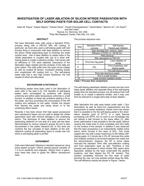
Step<br />
Standard POCl 3<br />
Self-doping<br />
process Paste/Laser Ablation<br />
1 Saw damage etch, texture, clean<br />
2 Diffusion in POCl 3 to ~50-80 Ω/□<br />
3 PSG removal<br />
4 SiN x deposition by PECVD<br />
5 Print front Ag paste<br />
Laser ablation of<br />
6 Dry<br />
nitride<br />
Print proprietary selfdoping<br />
paste<br />
7 Fire self-doping paste<br />
8 Print rear aluminum paste<br />
9 Fire in a belt furnace<br />
10 Laser junction isolation scribe<br />
Table 1 Process flow comparison<br />
The self-doping paste/laser ablation process has two more<br />
steps (laser ablation and separate firing of the self-doping<br />
paste) than the standard process, but we believe that it will<br />
enable us to create a selective emitter, and it may over<br />
time be reduced to a single extra step of laser ablation.<br />
After fabrication the cells were tested under static 1 Sun<br />
illumination as well as Suns-Voc measurement and the<br />
components of series resistance. Earlier work had shown<br />
that it is possible to fire the self-doping paste to the silversilicon<br />
eutectic point of 877°C in a rapid thermal<br />
processing unit (RTP), but no work to our knowledge has<br />
yet utilized a belt furnace to the same effect [1]. After<br />
some optimization it was possible to fire the paste, without<br />
causing the metal lines to melt completely and form balls<br />
on the surface of the sample. In addition it was observed<br />
that the laser processing in air inadvertently melted some<br />
silicon which formed a thin layer of SiO 2. This oxide<br />
capped the vias with a layer impervious to the fritless selfdoping<br />
paste. A 2 minute dip in 5% HF removed this oxide<br />
and enabled contacts to be formed between the metal and<br />
the semiconductor; however, the HF in some cases<br />
removed the standard 78nm SiN x anti-reflection coating<br />
and front passivation layer as well. Therefore a new<br />
process was developed in which thicker SiN x layers were<br />
deposited, ablated by the laser underneath the gridline<br />
locations, and then dipped the 5% HF solution. This<br />
solution completely removed the thin layer of oxide<br />
blocking the vias, but only partially etched away the SiN x.<br />
The cell efficiency results are shown in Figure 1 below.<br />
978-1-4244-5892-9/10/$26.00 ©2010 IEEE 003577
Eff(%)<br />
RESULTS & DISCUSSION<br />
The thicker nitride has had an adverse impact on the cell<br />
open circuit voltage. These samples did not have their<br />
nitride deposited in one continuous run, but were removed<br />
from the reactor in between shorter nitride depositions.<br />
Overall the cell open circuit voltage is much lower than our<br />
standard process which yields ~620mV. We hypothesize<br />
that the ~5 minutes the samples spend at 950°C during<br />
the self-doping paste firing is killing the sample bulk<br />
lifetime which accounts for this observed low V oc. A<br />
cleaner firing environment (e.g. RTA unit or cleaner<br />
furnace) should mitigate this problem.<br />
Figure 1 shows the solar cell efficiency as a function<br />
of different nitride thicknesses (in nm). Plus signs<br />
represent 45µJ/pulse and circles represent<br />
30µJ/pulse.<br />
FF(%)<br />
Comparing these cells’ efficiency to those of the baseline<br />
cells (see Table 2 below) shows the inadequacy of the<br />
current procedure.<br />
Cell<br />
Type<br />
Eff.<br />
(%)<br />
J sc<br />
(mA/cm 2 )<br />
V oc<br />
(mV)<br />
FF<br />
(%)<br />
R series<br />
(Ω·cm 2 )<br />
Std. 17.58 36.75 624 76.7 0.80<br />
New 13.19 32.53 566 71.7 1.80<br />
Table 2 best cell efficiency<br />
Figure 3 shows the fill factor of the cells. Control cells<br />
fabricated using a fritted paste had FF ~77% (see<br />
Table 2).<br />
Some of the difficulties encountered included aligning the<br />
screen-printed paste to the vias in the SiN x. This task was<br />
made easier by using a screen with wider than normal<br />
openings to print lines ~220µm wide instead of the<br />
standard ~110µm. This increase in line width caused<br />
increased shading and a resulting decrease in the short<br />
circuit current density by approximately 2 mA/cm 2 . In<br />
addition we observed an extra loss of another 2 mA/cm 2<br />
due to an unoptimized AR coating after the HF dip.<br />
Rser att (Ohm*cm2)<br />
Voc(V)<br />
Figure 4 shows the cell series resistance.<br />
Figure 2 shows the change in open circuit voltage<br />
with nitride thickness<br />
These values are coming from the higher than normal<br />
contact resistance. We have measured the other<br />
components of the series resistance, emitter sheet &<br />
gridlines being the two main ones. These components<br />
together contribute only ~0.5Ω·cm 2 to the normalized<br />
series resistance meaning that the contact resistance is<br />
still surprisingly large—larger than for the standard POCl 3<br />
process.<br />
978-1-4244-5892-9/10/$26.00 ©2010 IEEE 003578
Pseudo-FF<br />
more exact formulation from equation 1 does not change<br />
the results substantially. We have further correlated this<br />
indirect measurement of contact resistance with a<br />
measurement of the transfer length method. We cut up a<br />
finished cell into a 10mm wide strip by laser cutting on the<br />
rear and cleaving. The resistance was measured between<br />
adjacent gridlines and then plotted as a function of the<br />
number of gridline spacings.<br />
100<br />
TLM<br />
R = 65 Ohm/sq. (by 4 pt. probe)<br />
sheet<br />
R = 760 mOhm*cm 2 (metal area)<br />
contact<br />
80<br />
Figure 5 Pseudo-fill factor from the Suns-Voc<br />
measurement.<br />
60<br />
No HF strip<br />
y = 76 + 1.9x R= 0.4615<br />
Some slight decrease in PFF is observed for thicker<br />
nitrides, but in general these values are not so small<br />
compared to POCl 3 diffused cells with full Al rear.<br />
∆FF = -(J sc/V oc)·R series,tot·FF ideal (1)<br />
Equation (1) describes the loss in fill factor for a given cell<br />
with known J sc, V oc, and total area normalized series<br />
resistance [5]. For the cells described in this paper FF ideal<br />
≈ 0.8 in the best case. ∆FF = 0.083 for the self-doping<br />
paste cells and 0.038 for the control samples.<br />
The major cause of loss of fill factor is the increase in<br />
series resistance from 0.80 Ω·cm 2 up to 1.80Ω·cm 2 .<br />
Components<br />
Std. Self-doping<br />
Process Paste<br />
Grid 0.325 0.231<br />
Emitter 0.312 0.312<br />
Back Al 0.036 0.036<br />
Within busbar 0.004 0.004<br />
Substrate 0.032 0.032<br />
Sum of components 0.71 0.615<br />
Total (from I-V curve) 0.80 1.80<br />
Contact = Total – Sum 0.09 1.185<br />
Metal area specific<br />
contact resistance<br />
7.2 mΩ·cm 2 ~95 mΩ·cm 2<br />
Table 3 Components of Series Resistance in Ω·cm 2<br />
(cell area) except the last row.<br />
From Table 3 we observe that although the major<br />
components of series resistance are the grid and the<br />
emitter sheet resistance. For the standard, fritted paste the<br />
contact resistance is small relative to these two<br />
components. For the self-doping paste in contrast, the<br />
contact resistance is much larger than anticipated. This<br />
result implies a metal contact area specific contact<br />
resistance of nearly 100mΩ·cm 2 . Taking into account the<br />
40<br />
20<br />
5 min HF<br />
y = 1.85 + 12.342x R= 0.99968<br />
R = 51 Ohm/sq..<br />
sheet<br />
R = 18.5 mOhm*cm 2 (metal area)<br />
contact<br />
0<br />
0 1 2 3 4 5<br />
Spacing (Gridlines)<br />
Figure 6 plots resistance between gridlines as a<br />
function of spacing.<br />
The inset equations to Figure 6 are derived from linear<br />
fitting to the measured data. The slope of the equation<br />
confirms the emitter sheet resistance and the intercept is<br />
twice the contact resistance. The contact resistance has<br />
been normalized to the metal contact area for the two<br />
cases shown. The sample depicted in red did not have the<br />
laser-grown oxide stripped by HF and has a<br />
correspondingly high contact resistance. The sample<br />
depicted in blue had its nitride completely removed by 5<br />
minute HF dip and has a relatively low contact resistance.<br />
The indirectly calculated contact resistance values<br />
reported in Table 3 were confirmed to by this method.<br />
We have two interpretations of these results. Our first<br />
thought is that the laser may have damaged the diffused<br />
emitter layer. Ablation of a significant portion of the emitter<br />
means that the silver paste is trying to form an electrical<br />
contact with less heavily doped silicon which is known to<br />
be difficult. Furthermore because the paste is fritless, only<br />
that portion of the paste which is printed onto the via can<br />
contact the underlying silicon. The contact area of the selfdoping<br />
paste is less than that of the standard, fritted paste<br />
because the silver sinters only in those locations where<br />
the laser ablated the silicon nitride. Since this contact area<br />
is smaller than for the standard paste the contact<br />
resistance, other things being equal, should be greater.<br />
The entire point of the experiment is that the self-doping<br />
978-1-4244-5892-9/10/$26.00 ©2010 IEEE 003579
paste should allow lower contact resistance due to the<br />
presence of extra dopant underneath the metal contacts<br />
which can enable a selective emitter by decreasing the<br />
doping in the space between the gridlines. After confirming<br />
that the contact resistance was indeed very large, we were<br />
forced to ask the question whether the self-doping paste<br />
was functioning as named. To confirm the operation of the<br />
paste, we used the SIMS technique.<br />
alloying reaction of the Ag-Si on the mirror polished wafers<br />
did not take place uniformly as it did on the textured<br />
wafers. Micrographs showing the results are shown in<br />
Figure 7 after most of the paste was removed by a nitric<br />
acid solution followed by HF/HCl. For some portions of the<br />
sample all the silver was removed (upper photo), but for<br />
others the silver remained (lower photo).<br />
Figure 7 shows also the difficulty of obtaining accurate<br />
SIMS results given that the size of the alloyed areas is<br />
only ~25-50µm per side—still smaller than the SIMS ion<br />
beam. The alloying appears to take place only along the<br />
crystal planes. Ref 1 showed that the alloying resulted in<br />
triangles when the paste was printed on (111) oriented<br />
silicon. Here on the (100) silicon it alloys preferentially in<br />
rectangles.<br />
In Figure 8 below the concentration of phosphorus and<br />
silver are both shown as a function of depth. To our<br />
surprise the phosphorus concentration is lower than<br />
expected which can explain the large contact resistances<br />
observed. If there were truly an eutectic formation then we<br />
would expect a deep junction as as is observed for the<br />
eutectic formation with Al and Si on the rear of the cell.<br />
The phosphorus and silver are present only in a very<br />
shallow region indicating that we have not achieved true<br />
alloying in this case. The silver concentration is also<br />
significantly greater than anticipated in the silicon and<br />
might cause problems with shunting the device. Based on<br />
this data, coupled with the high measured contact<br />
resistance we conclude that we were unsuccessful in<br />
getting the silver-silicon interface to form the eutectic, or if<br />
so, only in small portions.<br />
SIMS Data for Self-doping Paste<br />
31-P Conc (cm -3 )<br />
Ag Conc (cm -3 )<br />
Figure 7 shows surface after firing and removal of the<br />
silver by acid etch. The area shown in both cases is<br />
225µm by 250µm. The upper photo also contains<br />
rough depth data with some pits as deep as 19 µm. In<br />
the lower photo the silver paste was not completely<br />
removed even after ultrasonic agitation in nitric acid.<br />
Secondary ion mass spectroscopy (SIMS) is not well<br />
suited to analyzing textured substrates since the size of<br />
the pyramids is smaller than the ion beam size in the<br />
SIMS measurement making it impossible to achieve any<br />
depth resolution. To overcome this difficulty (100) oriented<br />
mirror polished silicon wafers were processed similarly to<br />
the solar cells including SiN x deposition, laser ablation, HF<br />
dip, screen printing of the self-doping paste, and firing in a<br />
belt furnace. These samples were sent out for SIMS<br />
analysis. Diffusion was explicitly excluded on these<br />
samples so as to make the analysis easier. Any<br />
phosphorus measured in these samples must be<br />
attributed to the paste. Unfortunately after firing the<br />
10 21<br />
10 20<br />
10 19<br />
10 18<br />
10 17<br />
0 20 40 60 80 100<br />
Depth (nm)<br />
Figure 8 shows the concentration of phosphorus and<br />
silver as a function of depth. The silver is going<br />
deeper into the silicon and causing some shunting of<br />
the devices describe elsewhere in this report.<br />
978-1-4244-5892-9/10/$26.00 ©2010 IEEE 003580
CONCLUSIONS<br />
While the cells fabricated for this project were not better<br />
than the standard process and the contact resistance is<br />
still higher due to lack of significant phosphorus diffusion,<br />
we successfully used a laser ablation process to fabricate<br />
selective emitter solar cells on 125mm pseudo-square<br />
wafers. A peak cell efficiency of 13% was achieved. Cell<br />
efficiency was limited by lower open circuit voltage, most<br />
likely caused by decreased bulk lifetime, as well as low fill<br />
factor caused by increased series resistance. The<br />
decrease in J sc is explained well by the extra shading and<br />
unoptimized AR coating thickness. The analysis of the<br />
components of the series resistance indicates that contact<br />
resistance approximately 100 times greater for this<br />
process than for the standard fritted paste process. The<br />
root causes of this higher contact resistance are ablation<br />
of part of the emitter lowering the phosphorus<br />
concentration under the laser-ablated vias, decreased<br />
contact area due to the laser ablated holes being the only<br />
contact points and mainly that too little phosphorus<br />
diffused into the silicon underneath the gridlines.<br />
ACKNOWLEDGEMENTS<br />
This work is partially supported by the DOE under contract<br />
No. DE-EE0000584. We thank Alan Carroll of Dupont for<br />
a helpful discussion. Thanks also go to Don Tremblay for<br />
some of the measurements.<br />
REFERENCES<br />
[1] D. L. Meier et al., “Production of Thin (70-100 µm)<br />
Crystalline Silicon Cells for Conformable Modules,”<br />
29 th IEEE PVSC, 2002, pp. 110-113.<br />
[2] M. Hilali et al., “Optimization of Self-Doping Ag Paste<br />
Firing to Achieve High Fill Factors on Screen-Printed<br />
Silicon Solar Cells with a 100 Ω/sq. Emitter,” 29 th<br />
IEEE PVSC, 2002, pp. 356-359.<br />
[3] Peter Engelhart et al., “Laser Ablation of SiO 2 for<br />
Locally Contacted Si Solar Cells With Ultra-short<br />
Pulses,” Prog. Photovolt. Res. Appl. 15, 2007, pp.<br />
521–527.<br />
[4] Stuart Wenham and Martin Green, US Pat. 6,429,037<br />
B1.<br />
[5] D.L. Meier, E. A. Good, R. A. Garcia, B.L. Bingham,<br />
S. Yamanaka, V. Chandrasekaran, and C. Bucher,<br />
“Determining components of series resistance from<br />
measurements on a finished cell”, 32 th IEEE PVSC<br />
2006, pp. 1315-1318.<br />
978-1-4244-5892-9/10/$26.00 ©2010 IEEE 003581