Datasheet - Omron
Datasheet - Omron
Datasheet - Omron

Create successful ePaper yourself
Turn your PDF publications into a flip-book with our unique Google optimized e-Paper software.
CONTENTS<br />
Selection Guide . . . . . . . . . . . . . . . . . . . . . . . . . . . . . . . . . . . . 2<br />
Microphotonic Devices<br />
Manuscript Paper Sensors . . . . . . . . . . . . . . . . . . . . . . . . . . . . . . . . . 6<br />
Photomicrosensors<br />
Technical Information . . . . . . . . . . . . . . . . . . . . . . . . . . . . . . . . . . . . 12<br />
Precautions . . . . . . . . . . . . . . . . . . . . . . . . . . . . . . . . . . . . . . . . . . . . . 25<br />
Application Examples . . . . . . . . . . . . . . . . . . . . . . . . . . . . . . . . . . . . 28<br />
Transmissive Photomicrosensors . . . . . . . . . . . . . . . . . . . . . . . . . . . . 30<br />
Reflective Photomicrosensors . . . . . . . . . . . . . . . . . . . . . . . . . . . . . . 150<br />
General Information<br />
Reliability. . . . . . . . . . . . . . . . . . . . . . . . . . . . . . . . . . . . . . . . . . . . . . 176<br />
Security Trade Control . . . . . . . . . . . . . . . . . . . . . . . . . . . . . . . . . . . . 185<br />
1
Selection Guide<br />
Sensing<br />
method<br />
Sensing distance Model Output configuration Features Page<br />
Transmissive 1.0 mm EE-SX1107 Phototransistor Ultra-compact, surface mounting 62<br />
2.0 mm EE-SX1018 Phototransistor Compact, general purpose 30<br />
EE-SX1049 Phototransistor Compact, general purpose 40<br />
EE-SX1103 Phototransistor Ultra-compact, general purpose 56<br />
EE-SX1105 Phototransistor Ultra-compact, general purpose 58<br />
EE-SX1108 Phototransistor Ultra-compact, surface mounting 66<br />
EE-SX1131 Phototransistor Ultra-compact, surface mounting, dualchannel<br />
78<br />
output<br />
EE-SX4134 Photo-IC Ultra-compact, surface mounting 136<br />
EE-SX493 Photo-IC High resolution 130<br />
2.8 mm EE-SX1055 Phototransistor Compact, excellent cost performance 42<br />
3.0 mm EE-SX1046 Phototransistor With a horizontal aperture 38<br />
EE-SX1106 Phototransistor Ultra-compact, general purpose 60<br />
EE-SX1109 Phototransistor Ultra-compact, surface mounting 70<br />
EE-SX129 Phototransistor High resolution 88<br />
EE-SX198 Phototransistor General purpose 94<br />
EE-SX199 Phototransistor With a positioning boss 96<br />
EE-SX298 Photo-Darlington transistor General purpose 116<br />
EE-SX398/498 Photo-IC General purpose 132<br />
3.4 mm EE-SX1071 Phototransistor General purpose 48<br />
EE-SX1088 Phototransistor Screw mounting 52<br />
EE-SX1096 Phototransistor With a horizontal aperture 54<br />
EE-SX138 Phototransistor Screw mounting 90<br />
EE-SX153 Phototransistor Screw mounting 92<br />
EE-SH3 series Phototransistor Screw mounting 108<br />
EE-SJ3 series Phototransistor Screw mounting 110<br />
EE-SV3 series Phototransistor Screw mounting 114<br />
EE-SX301/401 Photo-IC General purpose 118<br />
EE-SX3088/4088 Photo-IC Screw mounting 124<br />
3.5 mm EE-SX384/484 Photo-IC General purpose 128<br />
3.6 mm EE-SX1057 Phototransistor Dust-proof construction, general purpose 44<br />
EE-SG3(-B) Phototransistor Dust-proof construction 106<br />
4.2 mm EE-SX1128 Phototransistor With a horizontal aperture 76<br />
5.0 mm EE-SX1041 Phototransistor General purpose 34<br />
EE-SX1042 Phototransistor High profile 36<br />
EE-SX1081 Phototransistor General purpose 50<br />
EE-SX1115 Phototransistor High profile with positioning pins 74<br />
EE-SX1137 Phototransistor General purpose 82<br />
EE-SX1235A-P2 Phototransistor Snap-in mounting 86<br />
5.0 mm EE-SJ5-B Phototransistor General purpose 112<br />
3.6 mm EE-SX3148-P1 Photo-IC Screw mounting 126<br />
2 Selection Guide
Sensing<br />
method<br />
Sensing distance Model Output configuration Features Page<br />
Transmissive 5.0 mm EE-SX3081/4081 Photo-IC General purpose 122<br />
EE-SX3239-P2 Photo-IC Snap-in mounting 142<br />
EE-SX3009-P1/ Photo-IC Screw mounting 134<br />
4009-P1<br />
EE-SX4235A-P2 Photo-IC Snap-in mounting 140<br />
EE-SX460-P1 Photo-IC Snap-in mounting 144<br />
5.2 mm EE-SX1035 Phototransistor Compact, wide 32<br />
8.0 mm EE-SX1070 Phototransistor General purpose 46<br />
EE-SX3070/4070 Photo-IC General purpose 120<br />
15.0 mm EE-SX461-P11 Photo-IC Easy to mount 146<br />
14 mm EE-SX1140 Phototransistor Wide, high profile 84<br />
Actuator mounting<br />
--- EE-SA102 Phototransistor General purpose 98<br />
EE-SA104 Phototransistor Compact 100<br />
EE-SA407-P2 Photo-IC Easy to mount 148<br />
Actuator --- EE-SA105 Phototransistor General purpose 102<br />
EE-SA113 Phototransistor General purpose 104<br />
Reflective 1.0 mm EE-SY193 Phototransistor Ultra-compact, surface mounting 162<br />
3.5 mm EE-SY171 Phototransistor Thin 160<br />
4.0 mm EE-SY169 Phototransistor High resolution (red LED) 154<br />
EE-SY169A Phototransistor High resolution (infrared LED) 156<br />
EE-SY169B Phototransistor High resolution (red LED) 158<br />
4.4 mm EE-SY113 Phototransistor Dust-proof 152<br />
EE-SY313/413 Photo-IC Dust-proof 172<br />
5.0 mm EE-SY110 Phototransistor General purpose 150<br />
EE-SB5(-B) Phototransistor Screw mounting 166<br />
EE-SF5(-B) Phototransistor Dust-proof 168<br />
EE-SY310/410 Photo-IC General purpose 170<br />
Selection Guide 3
4 Selection Guide
Microphotonic Devices<br />
Manuscript Paper Sensors<br />
EY3A-1051 . . . . . . . . . . . . . . . . . . . . . . . . . . . . . . . . . . . . . . . . . . . . . . . 6<br />
EY3A-1081 . . . . . . . . . . . . . . . . . . . . . . . . . . . . . . . . . . . . . . . . . . . . . . . 8<br />
5
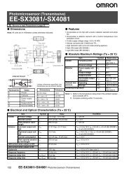
Manuscript Paper Sensor (1 Beam: 50 mm)<br />
EY3A-1051<br />
Be sure to read Precautions on page 25.<br />
■ Dimensions<br />
Note: All units are in millimeters unless otherwise indicated.<br />
Positioning boss Center of detector<br />
8.3 dia.<br />
■ Features<br />
• Ensures higher sensitivity and external light interference resistivity<br />
than any other photomicrosensor.<br />
• Narrow sensing range ensures stable sensing of a variety of sensing<br />
objects.<br />
■ Absolute Maximum Ratings (Ta = 25°C)<br />
8 dia.<br />
Pin no. Remarks<br />
Name<br />
7.9 dia.<br />
Center of emitter<br />
Pin no. 1<br />
3 +0<br />
-0.2 dia.<br />
1 O Output (OUT)<br />
2 V Power supply<br />
(Vcc)<br />
3 G Ground (GND)<br />
Unless otherwise specified, the<br />
tolerances are as shown below.<br />
3.2 +0.2<br />
-0 dia.<br />
0.5<br />
15<br />
Item Symbol Rated value<br />
Power supply voltage V CC 7 V<br />
Load voltage V OUT 7 V<br />
Load current I OUT 10 mA<br />
Ambient temperature<br />
Operating Topr 0°C to 60°C<br />
Storage Tstg –15°C to<br />
70°C<br />
Note: Make sure there is no icing or condensation when operating the<br />
Sensor.<br />
Dimensions Tolerance<br />
3 mm max. ±0.3<br />
3 < mm ≤ 6 ±0.375<br />
6 < mm ≤ 10 ±0.45<br />
10 < mm ≤ 18 ±0.55<br />
18 < mm ≤ 30 ±0.65<br />
30 < mm ≤ 50 ±0.8<br />
Recommended Mating Connectors:<br />
Japan Molex 51090-0300 (crimp connector)<br />
52484-0310 (press-fit connector)<br />
■ Electrical and Optical Characteristics (Ta = 0°C to 60°C)<br />
Item Value Condition<br />
Power supply voltage 5 V ±5% ---<br />
Current consumption 50 mA max. V CC = 5 V, R L = ∞<br />
Peak current consumption 200 mA max. V CC = 5 V, R L = ∞<br />
Low-level output voltage 0.6 V max. V CC = 5 V, I OL = 4 mA (see note 1)<br />
High-level output voltage 3.5 V min. V CC = 5 V, R L = 4.7 kΩ (see note 2)<br />
Response delay time (High to Low) 1.5 ms max. The time required for the output to become “Lo” after placing<br />
sensing object.<br />
Response delay time (Low to high) 1.5 ms max. The time required for the output to become “Hi” after removing<br />
sensing object.<br />
Note: 1. These conditions are for the sensing of lusterless paper with an OD of 0.9 maximum located at the correct sensing position of the Sensor<br />
as shown in the optical path arrangement on page 7.<br />
2. These conditions are for the sensing of the paper supporting plate with an OD of 0.05 located using the glass plate without paper as<br />
shown in the optical path arrangement on page 7.<br />
6 EY3A-1051 Manuscript Paper Sensor (1 Beam: 50 mm)
■ Characteristics (Paper Table Glass: t = 6 mm max., Transparency Rate: 90% min.)<br />
(Ta =0°C to 60°C)<br />
Sensing density<br />
Note: 1. The data shown are initial data.<br />
2. Optical darkness (OD) is defined by the following formula:<br />
P IN (mW):<br />
Item<br />
Light power incident upon the document<br />
P OUT (mW): Reflected light power from the document<br />
■ Optical Path Arrangement<br />
Characteristic value<br />
Lusterless paper with an OD of 0.9 max. (sensing distance: 50 mm) (see note)<br />
Non-sensing distance 85 mm (from the top of the sensor), OD: 0.05<br />
Paper sensing distance<br />
Ambient illumination<br />
OD = − log 10<br />
POUT<br />
PIN<br />
50 mm (from the top of the sensor)<br />
Sunlight: 3,000 lx max., fluorescent light: 2,000 lx max.<br />
85 (see note 2)<br />
10 dia.<br />
(see note 1)<br />
50 (standard value)<br />
8.9<br />
■ Engineering Data<br />
Distance Characteristics (Typical)<br />
Paper supporting plate<br />
Glass<br />
Note: 1. The part with oblique lines indicates the paper sensing area of the EY3A-1051, which is practically<br />
determined by the diameter of the beam and its tolerance.<br />
2. The non-sensing distance of the EY3A-1051 is determined using a paper with an OD of 0.05.<br />
4.75 V<br />
5.0 V<br />
5.25 V<br />
OD (value)<br />
Distance (mm)<br />
EY3A-1051 Manuscript Paper Sensor (1 Beam: 50 mm) 7
Manuscript Paper Sensor (1 Beam: 80 mm)<br />
EY3A-1081<br />
Be sure to read Precautions on page 25.<br />
■ Dimensions<br />
Note: All units are in millimeters unless otherwise indicated.<br />
Positioning boss<br />
Center of detector<br />
■ Features<br />
• Ensures higher sensitivity and external light interference resistivity<br />
than any other photomicrosensor.<br />
• Narrow sensing range ensures stable sensing of a variety of sensing<br />
objects.<br />
■ Absolute Maximum Ratings (Ta = 25°C)<br />
7.9 dia. 8.3 dia. Item Symbol Rated value<br />
Center of emitter<br />
Pin no.1<br />
3 0<br />
-0.2 dia.<br />
3.2 +0.2<br />
0 dia.<br />
Power supply voltage V CC 7 V<br />
Load voltage V OUT 7 V<br />
Load current I OUT 10 mA<br />
Ambient temperature<br />
Operating Topr 0°C to 60°C<br />
Storage Tstg –15°C to<br />
70°C<br />
Note: Make sure there is no icing or condensation when operating the<br />
Sensor.<br />
Pin no. Remarks Name<br />
1 O Output (OUT)<br />
2 V Power supply (Vcc)<br />
3 G Ground (GND)<br />
Unless otherwise specified, the<br />
tolerances are as shown below.<br />
Dimensions Tolerance<br />
3 mm max. ±0.3<br />
3 < mm ≤ 6 ±0.375<br />
6 < mm ≤ 10 ±0.45<br />
10 < mm ≤ 18 ±0.55<br />
18 < mm ≤ 30 ±0.65<br />
30 < mm ≤ 50 ±0.8<br />
Recommended Mating Connectors:<br />
Japan Molex 51090-0300 (crimp connector)<br />
52484-0310 (press-fit connector)<br />
50 < mm ≤ 80 ±0.95<br />
■ Electrical and Optical Characteristics (Ta = 0°C to 60°C)<br />
Item Value Condition<br />
Power supply voltage 5 V ±5% ---<br />
Current consumption 50 mA max. V CC = 5 V, R L = ∞<br />
Peak current consumption 200 mA max. V CC = 5 V, R L = ∞<br />
Low-level output voltage 0.6 V max. V CC = 5 V, I OL = 4 mA (see note 1)<br />
High-level output voltage 3.5 V min. V CC = 5 V, R L = 4.7 kΩ (see note 2)<br />
Response delay time (High to Low) 1.5 ms max. The time required for the output to become “Lo” after placing<br />
sensing object.<br />
Response delay time (Low to high) 1.5 ms max. The time required for the output to become “Hi” after removing<br />
sensing object.<br />
Note: 1. These conditions are for the sensing of lusterless paper with an OD of 0.7 maximum located at the correct sensing position of the Sensor<br />
as shown in the optical path arrangement on page 9.<br />
2. These conditions are for the sensing of the paper supporting plate with an OD of 0.05 located using the glass plate without paper as<br />
shown in the optical path arrangement on page 9.<br />
8 EY3A-1081 Manuscript Paper Sensor (1 Beam: 80 mm)
■ Characteristics (Paper Table Glass: t = 6 mm max., Transparency Rate: 90% min.)<br />
(Ta =0°C to 60°C)<br />
Sensing density<br />
Item<br />
Note: 1. The data shown are initial data.<br />
2. Optical darkness (OD) is defined by the following formula:<br />
P IN (mW):Light power incident upon the document<br />
P OUT (mW):Reflected light power from the document<br />
■ Optical Path Arrangement<br />
Characteristic value<br />
Lusterless paper with an OD of 0.7 max. (sensing distance: 80 mm) (see note)<br />
Non-sensing distance 120 mm (from the top of the sensor), OD: 0.05<br />
Paper sensing distance<br />
Ambient illumination<br />
OD = − log 10<br />
POUT<br />
PIN<br />
80 mm (from the top of the sensor)<br />
Sunlight: 3,000 lx max., fluorescent light: 2,000 lx max.<br />
120 (see note 2)<br />
10 dia. (see note 1)<br />
80 (Standard value)<br />
Note: 1. The part with oblique lines indicates the paper sensing area of the EY3A-1081, which is practically determined by the diameter of the<br />
beam and its tolerance.<br />
2. The non-sensing distance of the EY3A-1081 is determined using a paper with an OD of 0.05.<br />
■ Engineering Data<br />
Distance Characteristics (Typical)<br />
Paper supporting plate<br />
Glass<br />
OD (value)<br />
4.75 V<br />
5.0 V<br />
5.25 V<br />
Distance (mm)<br />
EY3A-1081 Manuscript Paper Sensor (1 Beam: 80 mm) 9
10 EY3A-1081 Manuscript Paper Sensor (1 Beam: 80 mm)
Photomicrosensors<br />
Transmissive Sensors<br />
Technical Information . . . . . . . . . . . . . . 12<br />
Precautions . . . . . . . . . . . . . . . . . . . . . 25<br />
Application Examples . . . . . . . . . . . . . . 28<br />
EE-SX1018. . . . . . . . . . . . . . . . . . . . . . 30<br />
EE-SX1035. . . . . . . . . . . . . . . . . . . . . . 32<br />
EE-SX1041. . . . . . . . . . . . . . . . . . . . . . 34<br />
EE-SX1042. . . . . . . . . . . . . . . . . . . . . . 36<br />
EE-SX1046. . . . . . . . . . . . . . . . . . . . . . 38<br />
EE-SX1049. . . . . . . . . . . . . . . . . . . . . . 40<br />
EE-SX1055. . . . . . . . . . . . . . . . . . . . . . 42<br />
EE-SX1057. . . . . . . . . . . . . . . . . . . . . . 44<br />
EE-SX1070. . . . . . . . . . . . . . . . . . . . . . 46<br />
EE-SX1071. . . . . . . . . . . . . . . . . . . . . . 48<br />
EE-SX1081. . . . . . . . . . . . . . . . . . . . . . 50<br />
EE-SX1088. . . . . . . . . . . . . . . . . . . . . . 52<br />
EE-SX1096. . . . . . . . . . . . . . . . . . . . . . 54<br />
EE-SX1103. . . . . . . . . . . . . . . . . . . . . . 56<br />
EE-SX1105. . . . . . . . . . . . . . . . . . . . . . 58<br />
EE-SX1106. . . . . . . . . . . . . . . . . . . . . . 60<br />
EE-SX1107. . . . . . . . . . . . . . . . . . . . . . 62<br />
EE-SX1108. . . . . . . . . . . . . . . . . . . . . . 66<br />
EE-SX1109. . . . . . . . . . . . . . . . . . . . . . 70<br />
EE-SX1115. . . . . . . . . . . . . . . . . . . . . . 74<br />
EE-SX1128. . . . . . . . . . . . . . . . . . . . . . 76<br />
EE-SX1131. . . . . . . . . . . . . . . . . . . . . . 78<br />
EE-SX1137. . . . . . . . . . . . . . . . . . . . . . 82<br />
EE-SX1140. . . . . . . . . . . . . . . . . . . . . . 84<br />
EE-SX1235A-P2. . . . . . . . . . . . . . . . . . 86<br />
EE-SX129. . . . . . . . . . . . . . . . . . . . . . . 88<br />
EE-SX138 . . . . . . . . . . . . . . . . . . . . . . 90<br />
EE-SX153 . . . . . . . . . . . . . . . . . . . . . . 92<br />
EE-SX198 . . . . . . . . . . . . . . . . . . . . . . 94<br />
EE-SX199 . . . . . . . . . . . . . . . . . . . . . . 96<br />
EE-SA102 . . . . . . . . . . . . . . . . . . . . . . 98<br />
EE-SA104 . . . . . . . . . . . . . . . . . . . . . . 100<br />
EE-SA105 . . . . . . . . . . . . . . . . . . . . . . 102<br />
EE-SA113 . . . . . . . . . . . . . . . . . . . . . . 104<br />
EE-SG3/EE-SG3-B . . . . . . . . . . . . . . . 106<br />
EE-SH3 Series. . . . . . . . . . . . . . . . . . . 108<br />
EE-SJ3 Series . . . . . . . . . . . . . . . . . . . 110<br />
EE-SJ5-B . . . . . . . . . . . . . . . . . . . . . . . 112<br />
EE-SV3 Series . . . . . . . . . . . . . . . . . . . 114<br />
EE-SX298 . . . . . . . . . . . . . . . . . . . . . . 116<br />
EE-SX301/-SX401 . . . . . . . . . . . . . . . . 118<br />
EE-SX3070/-SX4070 . . . . . . . . . . . . . . 120<br />
EE-SX3081/-SX4081 . . . . . . . . . . . . . . 122<br />
EE-SX3088/-SX4088 . . . . . . . . . . . . . . 124<br />
EE-SX3148-P1. . . . . . . . . . . . . . . . . . . 126<br />
EE-SX384/-SX484 . . . . . . . . . . . . . . . . 128<br />
EE-SX493 . . . . . . . . . . . . . . . . . . . . . . 130<br />
EE-SX398/498 . . . . . . . . . . . . . . . . . . . 132<br />
EE-SX3009-P1/-SX4009-P1 . . . . . . . . 134<br />
EE-SX4134 . . . . . . . . . . . . . . . . . . . . . 136<br />
EE-SX4235A-P2 . . . . . . . . . . . . . . . . . 140<br />
EE-SX3239-P2. . . . . . . . . . . . . . . . . . . 142<br />
EE-SX460-P1. . . . . . . . . . . . . . . . . . . . 144<br />
EE-SX461-P11. . . . . . . . . . . . . . . . . . . 146<br />
EE-SA407-P2. . . . . . . . . . . . . . . . . . . . 148<br />
Reflective Sensors<br />
EE-SY110. . . . . . . . . . . . . . . . . . . . . . . 150<br />
EE-SY113. . . . . . . . . . . . . . . . . . . . . . . 152<br />
EE-SY169. . . . . . . . . . . . . . . . . . . . . . . 154<br />
EE-SY169A . . . . . . . . . . . . . . . . . . . . . 156<br />
EE-SY169B . . . . . . . . . . . . . . . . . . . . . 158<br />
EE-SY171. . . . . . . . . . . . . . . . . . . . . . . 160<br />
EE-SY193. . . . . . . . . . . . . . . . . . . . . . . 162<br />
EE-SB5(-B). . . . . . . . . . . . . . . . . . . . . . 166<br />
EE-SF5(-B). . . . . . . . . . . . . . . . . . . . . . 168<br />
EE-SY310/-SY410 . . . . . . . . . . . . . . . . 170<br />
EE-SY313/-SY413 . . . . . . . . . . . . . . . . 172<br />
11
Technical Information<br />
Features of Photomicrosensors<br />
The Photomicrosensor is a compact optical sensor that senses objects or object positions with an optical beam. The transmissive Photomicrosensor<br />
and reflective Photomicrosensor are typical Photomicrosensors.<br />
The transmissive Photomicrosensor incorporates an emitter and a transmissive that face each other as shown in Figure 1. When an object is located<br />
in the sensing position between the emitter and the detector, the object intercepts the optical beam of the emitter, thus reducing the amount<br />
of optical energy reaching the detector.<br />
The reflective Photomicrosensor incorporates an emitter and a detector as shown in Figure 2. When an object is located in the sensing area of the<br />
reflective Photomicrosensor, the object reflects the optical beam of the emitter, thus changing the amount of optical energy reaching the detector.<br />
“Photomicrosensor” is an OMRON product name. Generally, the Photomicrosensor is called a photointerrupter.<br />
Figure 1. Transmissive Photomicrosensor<br />
Figure 2. Reflective Photomicrosensor<br />
LED Phototransistor LED Phototransistor<br />
<strong>Datasheet</strong><br />
■ Absolute Maximum Ratings and<br />
Electrical and Optical Characteristics<br />
The datasheets of Photomicrosensors include the absolute<br />
maximum ratings and electrical and optical characteristics of the<br />
Photomicrosensors as well as the datasheets of transistors and ICs.<br />
It is necessary to understand the difference between the absolute<br />
maximum ratings and electrical and optical characteristics of various<br />
Photomicrosensors.<br />
■ Absolute Maximum Ratings<br />
The absolute maximum ratings of Photomicrosensors and other<br />
products with semiconductors specify the permissible operating<br />
voltage, current, temperature, and power limits of these products.<br />
The products must be operated absolutely within these limits.<br />
Therefore, when using any Photomicrosensor, do not ignore the<br />
absolute maximum ratings of the Photomicrosensor, or the<br />
Photomicrosensor will not operate precisely. Furthermore, the<br />
Photomicrosensor may be deteriorate or become damaged, in which<br />
case OMRON will not be responsible.<br />
Practically, Photomicrosensors should be used so that there will be<br />
some margin between their absolute maximum ratings and actual<br />
operating conditions.<br />
■ Electrical and Optical Characteristics<br />
The electrical and optical characteristics of Photomicrosensors<br />
indicate the performance of Photomicrosensors under certain<br />
conditions. Most items of the electrical and optical characteristics<br />
are indicated by maximum or minimum values. OMRON usually<br />
sells Photomicrosensors with standard electrical and optical<br />
characteristics. The electrical and optical characteristics of<br />
Photomicrosensors sold to customers may be changed upon<br />
request. All electrical and optical characteristic items of<br />
Photomicrosensors indicated by maximum or minimum values are<br />
checked and those of the Photomicrosensors indicated by typical<br />
values are regularly checked before shipping so that OMRON can<br />
guarantee the performance of the Photomicrosensors.<br />
In short, the absolute maximum ratings indicate the permissible<br />
operating limits of the Photomicrosensors and the electrical<br />
and optical characteristics indicate the maximum performance<br />
of the Photomicrosensors.<br />
12 Technical Information
Terminology<br />
The terms used in the datasheet of each Photomicrosensor with a phototransistor output circuit or a photo IC output circuit are explained below.<br />
■ Phototransistor Output Photomicrosensor<br />
Symbol Item Definition<br />
I FP Pulse forward current The maximum pulse current that is allowed to flow continuously from the anode to cathode of an LED<br />
under a specified temperature, a repetition period, and a pulse width condition.<br />
I C Collector current The current that flows to the collector junction of a phototransistor.<br />
P C Collector dissipation The maximum power that is consumed by the collector junction of a phototransistor.<br />
I D Dark current The current leakage of the phototransistor when a specified bias voltage is imposed on the phototransistor<br />
so that the polarity of the collector is positive and that of the emitter is negative on condition that<br />
the illumination of the Photomicrosensor is 0 lx.<br />
I L Light current The collector current of a phototransistor under a specified input current condition and at a specified<br />
bias voltage.<br />
V CE (sat)<br />
Collector-emitter saturated<br />
voltage<br />
The ON-state voltage between the collector and emitter of a phototransistor under a specified bias current<br />
condition.<br />
I LEAK Leakage current The collector current of a phototransistor under a specified input current condition and at a specified<br />
bias voltage when the phototransistor is not exposed to light.<br />
tr Rising time The time required for the leading edge of an output waveform of a phototransistor to rise from 10% to<br />
90% of its final value when a specified input current and bias condition is given to the phototransistor.<br />
tf Falling time The time required for the trailing edge of an output waveform of a phototransistor to decrease from 90%<br />
to 10% of its final value when a specified input current and bias condition is given to the phototransistor.<br />
V CEO Collector-emitter voltage The maximum positive voltage that can be applied to the collector of a phototransistor with the emitter<br />
at reference potential.<br />
V ECO Emitter-collector voltage The maximum positive voltage that can be applied to the emitter of a phototransistor with the collector<br />
at reference potential.<br />
■ Phototransistor/Photo IC Output Photomicrosensor<br />
Symbol Item Definition<br />
I F Forward current The maximum DC voltage that is allowed to flow continuously from the anode of the LED to the cathode<br />
of the LED under a specified temperature condition.<br />
V R Reverse voltage The maximum negative voltage that can be applied to the anode of the LED with the cathode at reference<br />
potential.<br />
V CC Supply voltage The maximum positive voltage that can be applied to the voltage terminals of the photo IC with the<br />
ground terminal at reference potential.<br />
V OUT Output voltage The maximum positive voltage that can be applied to the output terminal with the ground terminal of<br />
the photo IC at reference potential.<br />
I OUT Output current The maximum current that is allowed to flow in the collector junction of the output transistor of the photo<br />
IC.<br />
P OUT Output permissible dissipation<br />
The maximum power that is consumed by the collector junction of the output transistor of the photo IC.<br />
V F Forward voltage The voltage drop across the LED in the forward direction when a specified bias current is applied to<br />
the photo IC.<br />
I R Reverse current The reverse leakage current across the LED when a specified negative bias is applied to the anode<br />
with the cathode at reference potential.<br />
V OL Output low voltage The voltage drop in the output of the photo IC when the IC output is turned ON under a specified voltage<br />
and output current applied to the photo IC.<br />
V OH Output high voltage The voltage output by the photo IC when the IC output is turned OFF under a specified supply voltage<br />
and bias condition given to the photo IC.<br />
I CC Current consumption The current that will flow into the sensor when a specified positive bias voltage is applied from the power<br />
source with the ground of the photo IC at reference potential.<br />
I FT<br />
(I FT OFF )<br />
I FT<br />
(I FT ON )<br />
LED current when output is<br />
turned OFF<br />
LED current when output is<br />
turned ON<br />
The forward LED current value that turns OFF the output of the photo IC when the forward current to<br />
the LED is increased under a specified voltage applied to the photo IC.<br />
The forward LED current value that turns ON the output of the photo IC when the forward current to<br />
the LED is increased under a specified voltage applied to the photo IC.<br />
ΔH Hysteresis The difference in forward LED current value, expressed in percentage, calculated from the respective<br />
forward LED currents when the photo IC is turned ON and when the photo IC is turned OFF.<br />
f Response frequency The number of revolutions of a disk with a specified shape rotating in the light path, expressed by the<br />
number of pulse strings during which the output logic of the photo IC can be obtained under a specified<br />
bias condition given to the LED and photo IC (the number of pulse strings to which the photo IC can<br />
respond in a second).<br />
Technical Information 13
Design<br />
The following explains how systems using Photomicrosensors must<br />
be designed.<br />
■ Emitter<br />
Characteristics of Emitter<br />
The emitter of each Photomicrosensor has an infrared LED or red<br />
LED. Figure 3 shows how the LED forward current characteristics of<br />
the EE-SX1018, which has an emitter with an infrared LED, and<br />
those of the EE-SY169B, which has an emitter with a red LED, are<br />
changed by the voltages imposed on the EE-SX1018 and EE-<br />
SY169B. As shown in this figure, the LED forward current<br />
characteristics of the EE-SX1018 greatly differ from those of the EE-<br />
SY169B. The LED forward current characteristics of any<br />
Photomicrosensor indicate how the voltage drop of the LED<br />
incorporated by the emitter of the Photomicrosensor is changed by<br />
the LED’s forward current (I F ) flowing from the anode to cathode.<br />
Figure 3 shows that the forward voltage (V F ) of the red LED is higher<br />
than that of the infrared LED.<br />
The forward voltage (V F ) of the infrared LED is approximately 1.2 V<br />
and that of the red LED is approximately 2 V provided that the<br />
practical current required by the infrared LED and that required by<br />
the red LED flow into these LEDs respectively.<br />
Driving Current Level<br />
It is especially important to decide the level of the forward current (I F )<br />
of the emitter incorporated by any Photomicrosensor. The forward<br />
current must not be too large or too small.<br />
Before using any Photomicrosensor, refer to the absolute maximum<br />
ratings in the datasheet of the Photomicrosensor to find the emitter’s<br />
forward current upper limit. For example, the first item in the<br />
absolute maximum ratings in the datasheet of the EE-SX1018<br />
shows that the forward current (I F ) of its emitter is 50 mA at a Ta<br />
(ambient temperature) of 25°C. This means the forward current (I F )<br />
of the emitter is 50 mA maximum at a Ta of 25°C. As shown in<br />
Figure 4, the forward current must be reduced according to changes<br />
in the ambient temperature.<br />
Figure 4 indicates that the forward current (I F ) is approximately<br />
27 mA maximum if the EE-SX1018 is used at a Ta of 60°C. This<br />
means that a current exceeding 27 mA must not flow into the emitter<br />
incorporated by the EE-SX1018 at a Ta of 60°C.<br />
As for the lower limit, a small amount of forward current will be<br />
required because the LED will not give any output if the forward<br />
current I F is zero.<br />
Figure 4. Temperature Characteristics (EE-SX1018)<br />
P C<br />
Figure 3. LED Forward Current vs. Forward Voltage<br />
Characteristics (Typical)<br />
Forward current IF (mA)<br />
EE-SX1018 (infrared LED)<br />
EE-SY169B (red LED)<br />
Forward current IF (mA)<br />
I F<br />
Collector dissipation PC (mW)<br />
Forward Voltage V F<br />
Forward voltage V F (V)<br />
2.4<br />
Ambient temperature Ta (°C)<br />
In short, the forward current lower limit of the emitter of any<br />
Photomicrosensor must be 5 mA minimum if the emitter has an<br />
infrared LED and 2 mA minimum if the emitter has a red LED. If the<br />
forward current of the emitter is too low, the optical output of the<br />
emitter will not be stable. To find the ideal forward current value of<br />
the Photomicrosensor, refer to the light current (I L ) shown in the<br />
datasheet of the Photomicrosensor. The light current (I L ) indicates<br />
the relationship between the forward current (I F ) of the LED<br />
incorporated by the Photomicrosensor and the output of the LED.<br />
The light current (I L ) is one of the most important characteristics. If<br />
the forward current specified by the light current (I L ) flows into the<br />
emitter, even though there is no theoretical ground, the output of the<br />
emitter will be stable. This characteristic makes it possible to design<br />
the output circuits of the Photomicrosensor easily. For example, the<br />
datasheet of EE-SX1018 indicates that a forward current (I F ) of 20<br />
mA is required.<br />
14 Technical Information
Design Method<br />
The following explains how the constants of a Photomicrosensor<br />
must be determined. Figure 5 shows a basic circuit that drives the<br />
LED incorporated by a Photomicrosensor.<br />
The basic circuit absolutely requires a limiting resistor (R). If the LED<br />
is imposed with a forward bias voltage without the limiting resistor,<br />
the current of the LED is theoretically limitless because the forward<br />
impedance of the LED is low. As a result the LED will burn out.<br />
Users often ask OMRON about the appropriate forward voltage to<br />
be imposed on the LED incorporated by each Photomicrosensor<br />
model that they use. There is no upper limit of the forward voltage<br />
imposed on the LED provided that an appropriate limiting resistor is<br />
connected to the LED. There is, however, the lower limit of the<br />
forward voltage imposed on the LED. As shown in Figure 3, the<br />
lower limit of the forward voltage imposed on the LED must be at<br />
least 1.2 to 2 V, or no forward current will flow into the LED. The<br />
supply voltage of a standard electronic circuit is 5 V minimum.<br />
Therefore, a minimum of 5 V should be imposed on the LED. A<br />
system incorporating any Photomicrosensor must be designed by<br />
considering the following.<br />
1. Forward current (I F )<br />
2. Limiting resistor (R) (refer to Figure 5)<br />
As explained above, determine the optimum level of the forward<br />
current (I F ) of the LED. The forward current (I F ) of the EE-SX1018,<br />
for example, is 20 mA. Therefore, the resistance of the limiting<br />
resistor connected to the LED must be decided so that the forward<br />
current of the LED will be approximately 20 mA. The resistance of<br />
the limiting resistor is obtained from the following.<br />
The positions of the limiting resistor (R) and the LED in Figure 5 are<br />
interchangeable. If the LED is imposed with reverse voltages<br />
including noise and surge voltages, add a rectifier diode to the circuit<br />
as shown in Figure 6. LEDs can be driven by pulse voltages, the<br />
method of which is, however, rarely applied to Photomicrosensors.<br />
In short, the following are important points required to operate any<br />
Photomicrosensor.<br />
A forward voltage (V F ) of approximately 1.2 V is required if the<br />
Photomicrosensor has an infrared LED and a forward voltage (V F ) of<br />
approximately 2 V is required if the Photomicrosensor has a red<br />
LED.<br />
The most ideal level of the forward current (I F ) must flow into the<br />
LED incorporated by the Photomicrosensor.<br />
Decide the resistance of the limiting resistor connected to the LED<br />
after deciding the value of the forward current (I F ).<br />
If the LED is imposed with a reverse voltage, connect a rectifier<br />
diode to the LED in parallel with and in the direction opposite to the<br />
direction of the LED.<br />
Figure 6. Reverse Voltage Protection Circuit<br />
R = V CC − V F<br />
I F<br />
In this case 5 V must be substituted for the supply voltage (V CC ). The<br />
forward voltage (V F ) obtained from Figure 3 is approximately 1.2 V<br />
when the forward current (I F ) of the LED is 20 mA. Therefore, the<br />
following resistance is obtained.<br />
V CC − V F 5 to 1.2 V<br />
R =<br />
I<br />
= = 190 Ω<br />
F 20 mA<br />
= approx. 180 to 220 Ω<br />
The forward current (I F ) varies with changes in the supply voltage<br />
(V CC ), forward voltage (V F ), or resistance. Therefore, make sure that<br />
there is some margin between the absolute maximum ratings and<br />
the actual operating conditions of the Photomicrosensor.<br />
Figure 5. Basic Circuit<br />
V CC<br />
I F<br />
R<br />
VF<br />
GND (ground)<br />
Technical Information 15
■ Design of Systems Incorporating<br />
Photomicrosensors (1)<br />
Phototransistor Output<br />
Characteristics of Detector Element<br />
The changes in the current flow of the detector element with and<br />
without an optical input are important characteristics of a detector<br />
element. Figure 7 shows a circuit used to check how the current flow<br />
of the phototransistor incorporated by a Photomicrosensor is<br />
changed by the LED with or without an appropriate forward current<br />
(I F ) flow, provided that the ambient illumination of the<br />
Photomicrosensor is ideal (i.e., 0 lx). When there is no forward<br />
current (I F ) flowing into the LED or the optical beam emitted from the<br />
LED is intercepted by an opaque object, the ammeter indicates<br />
several nanoamperes due to a current leaking from the<br />
phototransistor. This current is called the dark current (I D ). When the<br />
forward current (I F ) flows into the LED with no object intercepting the<br />
optical beam emitted from the LED, the ammeter indicates several<br />
milliamperes. This current is called the light current (I L ).<br />
The difference between the dark current and light current is 10 6<br />
times larger as shown below.<br />
• When optical beam to the phototransistor is interrupted<br />
Dark current I D : 10 –9 A<br />
• When optical beam to the phototransistor is not interrupted<br />
Light current I L : 10 –3 A<br />
The standard light current of a phototransistor is 10 6 times as large<br />
as the dark current of the phototransistor. This difference in current<br />
can be applied to the sensing of a variety of objects.<br />
Figure 7. Measuring Circuit<br />
Ammeter<br />
The ambient illumination of the LED and phototransistor<br />
incorporated by the Photomicrosensor in actual operation is not 0 lx.<br />
Therefore, a current larger than the dark current of the<br />
phototransistor will flow into the phototransistor when the optical<br />
beam emitted from the LED is interrupted. This current is rather<br />
large and must not be ignored if the Photomicrosensor has a<br />
photoelectric Darlington transistor, which is highly sensitive, as the<br />
detector element of the Photomicrosensor. The dark current of the<br />
phototransistor incorporated by any reflective Photomicrosensor<br />
flows if there is no reflective object in the sensing area of the<br />
reflective Photomicrosensor. Furthermore, due to the structure of the<br />
reflective Photomicrosensor, a small portion of the optical beam<br />
emitted from the LED reaches the phototransistor after it is reflected<br />
inside the reflective Photomicrosensor. Therefore, the dark current<br />
and an additional current will flow into the phototransistor if there is<br />
no sensing object in the sensing area. This additional current is<br />
called leakage current (I LEAK ). The leakage current of the<br />
phototransistor is several hundred nanoamperes and the dark<br />
current of the phototransistor is several nanoamperes.<br />
The dark current temperature and light current temperature<br />
dependencies of the phototransistor incorporated by any<br />
Photomicrosensor must not be ignored. The dark current<br />
temperature dependency of the phototransistor increases when the<br />
ambient temperature of the Photomicrosensor in operation is high or<br />
the Photomicrosensor has a photoelectric Darlington transistor as<br />
the detector element of the Photomicrosensor. Figure 8 shows the<br />
dark current temperature dependency of the phototransistor<br />
incorporated by the EE-SX1018.<br />
Dark current ID<br />
Figure 8. Dark Current vs. Ambient Temperature<br />
Characteristics (Typical) (EE-SX1018)<br />
V CE = 10 V<br />
0 lx<br />
Ambient temperature Ta (°C)<br />
Due to the temperature dependency of the phototransistor, the light<br />
current (I L ) of the phototransistor as the detector element of the<br />
Photomicrosensor increases according to a rise in the ambient<br />
temperature. As shown in Figure 9, however, the output of the LED<br />
decreases according to a rise in the ambient temperature due to the<br />
temperature dependency of the LED. An increase in the light current<br />
of the phototransistor is set off against a decrease in the output of<br />
the LED and consequently the change of the output of the<br />
Photomicrosensor according to the ambient temperature is<br />
comparatively small. Refer to Figure 10 for the light current<br />
temperature dependency of the phototransistor incorporated by the<br />
EE-SX1018.<br />
The light current temperature dependency shown in Figure 10 is,<br />
however, a typical example. The tendency of the light current<br />
temperature dependency of each phototransistor is indefinite. This<br />
means the temperature compensation of any Photomicrosensor is<br />
difficult.<br />
16 Technical Information
Figure 9. LED and Phototransistor Temperature<br />
Characteristics (Typical)<br />
Relative value (%)<br />
Ambient temperature Ta (°C)<br />
Figure 10. Relative Light Current vs. Ambient<br />
Temperature Characteristics (EE-SX1018)<br />
Relative light current (%)<br />
LED optical<br />
output<br />
Phototransistor light<br />
current<br />
Measurement condition<br />
I F = 20 mA<br />
V CE = 5 V<br />
A relative value of 100 is<br />
based on a Ta of 25°C.<br />
Ambient temperature Ta (°C)<br />
Changes in Characteristics<br />
The following explains the important points required for the<br />
designing of systems incorporating Photomicrosensors by<br />
considering worst case design technique. Worst case design<br />
technique is a method to design systems so that the<br />
Photomicrosensors will operate normally even if the characteristics<br />
of the Photomicrosensors are at their worst. A system incorporating<br />
any Photomicrosensor must be designed so that they will operate<br />
even if the light current (I L ) of the phototransistor is minimal and the<br />
dark current (I D ) and leakage current of the phototransistor are<br />
maximal. This means that the system must be designed so that it will<br />
operate even if the difference in the current flow of the<br />
phototransistor between the time that the Photomicrosensor senses<br />
an object and the time that the Photomicrosensor does not sense<br />
the object is minimal.<br />
The worst light current (I L ) and dark current (I D ) values of the<br />
phototransistor incorporated by any Photomicrosensor is specified in<br />
the datasheet of the Photomicrosensor. (These values are specified<br />
in the specifications either as the minimum value or maximum<br />
value.)<br />
Table 1 shows the dark current (I D ) upper limit and light current (I L )<br />
lower limit values of the phototransistors incorporated by a variety of<br />
Photomicrosensors.<br />
Systems must be designed by considering the dark current (I D )<br />
upper limit and light current (I L ) lower limit values of the<br />
phototransistors. Not only these values but also the following factors<br />
must be taken into calculation to determine the upper limit of the<br />
dark current (I D ) of each of the phototransistors.<br />
• External light interference<br />
• Temperature rise<br />
• Power supply voltage<br />
• Leakage current caused by internal light reflection if the systems<br />
use reflective Photomicrosensors.<br />
The above factors increase the dark current (I D ) of each<br />
phototransistor.<br />
As for the light current (I L ) lower limit of each phototransistor, the<br />
following factors must be taken into calculation.<br />
• Temperature change<br />
• Secular change<br />
The above factors decrease the light current (I L ) of each<br />
phototransistor.<br />
Table 2 shows the increments of the dark current (I D ) and the<br />
decrements of the light current (I D ) of the phototransistors.<br />
Therefore, if the EE-SX1018 is operated at a Ta of 60°C maximum<br />
and a V CC of 10 V for approximately 50,000 hours, for example, the<br />
dark current (I D ) of the phototransistor incorporated by the EE-<br />
SX1018 will be approximately 4 μA and the light current (I L ) of the<br />
phototransistor will be approximately 0.5 mA because the dark<br />
current (I D ) of the phototransistor at a Ta of 25°C is 200<br />
nanoamperes maximum and the light current (I L ) of the<br />
phototransistor at a Ta of 25°C is 0.5 mA minimum.<br />
Table 3 shows the estimated worst values of a variety of<br />
Photomicrosensors, which must be considered when designing<br />
systems using these Photomicrosensors.<br />
The dispersion of the characteristics of the Photomicrosensors must<br />
be also considered, which is explained in detail later. The light<br />
current (I L ) of the phototransistor incorporated by each reflective<br />
Photomicrosensor shown in its datasheet was measured under the<br />
standard conditions specified by OMRON for its reflective<br />
Photomicrosensors. The light current (I L ) of any reflective<br />
Photomicrosensor greatly varies with its sensing object and sensing<br />
distance.<br />
Technical Information 17
Table 1. Rated Dark Current (I D ) and Light Current (I L ) Values<br />
Model Upper limit (I D ) Lower limit (I L ) Condition<br />
EE-SG3(-B) 200 nA 2 mA I F = 15 mA<br />
EE-SX1018, -SX1055<br />
200 nA 0.5 mA I F = 20 mA<br />
EE-SX1041, -SX1042<br />
EE-SX1070, -SX1071<br />
EE-SX198, -SX199<br />
EE-SB5(-B)<br />
200 nA 0.2 mA I F = 20 mA (see note)<br />
EE-SF5(-B)<br />
EE-SY110<br />
Condition<br />
V CE = 10 V, 0 lx<br />
Ta = 25°C<br />
V CE = 10 V<br />
Ta = 25°C<br />
---<br />
Note: These values were measured under the standard conditions specified by OMRON for the corresponding Photomicrosensors.<br />
Table 2. Dependency of Detector Elements on Various Factors<br />
Elements Phototransistor Photo-Darlington transistor<br />
Dark current I D External light interference To be checked using experiment To be checked using experiment<br />
Temperature rise<br />
Increased by approximately 10 times with<br />
a temperature rise of 25°C.<br />
Increased by approximately 28 times with<br />
a temperature rise of 25°C.<br />
Supply voltage See Figure 11. See Figure 12.<br />
Light current I L Temperature change Approximately –20% to 10% Approximately –20% to 10%<br />
Secular change<br />
(20,000 to 50,000 hours)<br />
Note: For an infrared LED.<br />
Figure 11. Dark Current Imposed Voltage Dependency<br />
(Typical) (EE-SX1018)<br />
Decreased to approximately one-half of<br />
the initial value considering the temperature<br />
changes of the element.<br />
Decreased to approximately one-half of<br />
the initial value considering the temperature<br />
changes of the element.<br />
Relative dark current ID (%)<br />
A relative dark current value of 100<br />
is based on a Ta of 25°C and a V CE<br />
of 10 V.<br />
Collector-emitter voltage V CE (V)<br />
18 Technical Information
Table 3. Estimated Worst Values of a Variety of Photomicrosensors<br />
Model Estimated worst value (I D ) Estimated worst value (I L ) Condition<br />
EE-SG3(-B) 4 nA 1 mA I F = 15 mA<br />
EE-SX1018, -SX1055<br />
4 nA 0.25 mA I F = 20 mA<br />
EE-SX1041, -SX1042<br />
EE-SX1070, -SX1071<br />
EE-SX198, -SX199<br />
EE-SB5(-B)<br />
4 nA 0.1 mA I F = 20 mA (see note)<br />
EE-SF5(-B)<br />
EE-SY110<br />
Condition<br />
V CE = 10 V, 0 lx<br />
Ta = 60°C<br />
V CE = 10 V,<br />
Operating hours = 50,000 to<br />
100,000 hrs<br />
Ta = Topr<br />
---<br />
Note: These values were measured under the standard conditions specified by OMRON for the corresponding Photomicrosensors with an Infrared<br />
LED.<br />
Design of Basic Circuitry<br />
The following explains the basic circuit incorporated by a typical<br />
Photomicrosensor and the important points required for the basic<br />
circuit.<br />
The flowing currents (i.e., I L and I D ) of the phototransistor<br />
incorporated by the Photomicrosensor must be processed to obtain<br />
the output of the Photomicrosensor. Refer to Figure 13 for the basic<br />
circuit. The light current (I L ) of the phototransistor will flow into the<br />
resistor (R L ) if the phototransistor receives an optical input and the<br />
dark current (I D ) and leakage current of the phototransistor will flow<br />
into the resistor (R L ) if the phototransistor does not receive any<br />
optical input. Therefore, if the phototransistor receives an optical<br />
input, the output voltage imposed on the resistor (R L ) will be<br />
obtained from the following.<br />
IL x RL<br />
If the phototransistor does not receive any optical input, the output<br />
voltage imposed on the resistor (R L ) will be obtained from the<br />
following.<br />
(I D + leakage current) x R L<br />
The output voltage of the phototransistor is obtained by simply<br />
connecting the resistor (R L ) to the phototransistor. For example, to<br />
obtain an output of 4 V minimum from the phototransistor when it is<br />
ON and an output of 1 V maximum when the phototransistor is OFF<br />
on condition that the light current (I L ) of the phototransistor is 1 mA<br />
and the leakage current of the phototransistor is 0.1 mA, and these<br />
are the worst light current and leakage current values of the<br />
phototransistor, the resistance of the resistor (R L ) must be<br />
approximately 4.7 kΩ. Then, an output of 4.7 V (i.e., 1 mA x 4.7 kΩ)<br />
will be obtained when the phototransistor is ON and an output of<br />
0.47 V (i.e., 0.1 mA x 4.7 kΩ) will be obtained when the<br />
phototransistor is OFF. Practically, the output voltage of the<br />
phototransistor will be more than 4.7 V when the phototransistor is<br />
ON and less than 0.47 V when the phototransistor is OFF because<br />
the above voltage values are based on the worst light current and<br />
leakage current values of the phototransistor. The outputs obtained<br />
from the phototransistor are amplified and input to ICs to make<br />
practical use of the Photomicrosensor.<br />
Figure 13. Basic Circuit<br />
Figure 14. Output Example<br />
or<br />
Output<br />
V CC = 10 V<br />
Output voltage<br />
R L = 4.7 kΩ<br />
EE-SX1018<br />
Technical Information 19
Design of Applied Circuit<br />
The following explains the designing of the applied circuit shown in<br />
Figure 15.<br />
The light current (I L ) of the phototransistor flows into R 1 and R 2 when<br />
the phototransistor receives the optical beam emitted from the LED.<br />
Part of the light current (I L ) will flow into the base and emitter of Q 1<br />
when the voltage imposed on R 2 exceeds the bias voltage (i.e.,<br />
approximately 0.6 to 0.9 V) imposed between the base and emitter<br />
of the transistor (Q 1 ). The light current flowing into the base turns Q 1<br />
ON. A current will flow into the collector of Q 1 through R 3 when Q 1 is<br />
ON. Then, the electric potential of the collector will drop to a low<br />
logic level. The dark current and leakage current of the<br />
phototransistor flow when the optical beam emitted from the LED is<br />
intercepted. The electric potential of the output of the phototransistor<br />
(i.e., (I D + leakage current) x R 2 ) is, however, lower than the bias<br />
voltage between the base and emitter of Q 1 . Therefore, no current<br />
will flow into the base of Q 1 and Q 1 will be OFF. The output of Q 1 will<br />
be at a high level. As shown in Figure 16, when the phototransistor<br />
is ON, the phototransistor will be seemingly short-circuited through<br />
the base and emitter of the Q 1 , which is equivalent to a diode, and if<br />
the light current (I L ) of the phototransistor is large and R 1 is not<br />
connected to the phototransistor, the light current (I L ) will flow into Q 1<br />
and the collector dissipation of the phototransistor will be<br />
excessively large.<br />
The following items are important when designing the above applied<br />
circuit:<br />
• The voltage output (i.e., I L x R 2 ) of the phototransistor receiving the<br />
optical beam emitted from the LED must be much higher than the<br />
bias voltage between the base and emitter of Q 1 .<br />
• The voltage output (i.e., (I D + leakage current) x R 2 ) of the phototransistor<br />
not receiving the optical beam emitted from the LED<br />
must be much lower than the bias voltage between the base and<br />
emitter of Q 1 .<br />
Therefore, it is important to determine the resistance of R 2 . Figure 17<br />
shows a practical applied circuit example using the EE-SX1018<br />
Photomicrosensor at a supply voltage (V CC ) of 5V to drive a 74-<br />
series TTL IC. This applied circuit example uses R 1 and R 2 with<br />
appropriate resistance values.<br />
Figure 15. Applied Circuit<br />
EE-SX1018<br />
Figure 16. Equivalent Circuit<br />
Output<br />
Figure 17. Applied Circuit Example<br />
EE-SX1018<br />
R 1<br />
200 Ω<br />
I C1<br />
R 2<br />
10 kΩ<br />
Calculation of R 2<br />
The resistance of R 2 should be decided using the following so that<br />
the appropriate bias voltage (V BE (ON)) between the base and<br />
emitter of the transistor (Q 1 ) to turn Q 1 ON will be obtained.<br />
I C1 × R 2 > V BE(ON)<br />
I C1 = I L − I B<br />
∴(I L − I B ) x R2 > V BE(ON)<br />
V BE(ON)<br />
∴R 2 ><br />
I L − I B<br />
The bias voltage (V BE (ON)) between the base and emitter of Q 1 is<br />
approximately 0.8 V and the base current (I B ) of Q 1 is approximately<br />
20 μA if Q 1 is a standard transistor controlling small signals. The<br />
estimated worst value of the light current (I L ) of the phototransistor is<br />
0.25 mA according to Table 3.<br />
Therefore, the following is obtained.<br />
0.8 V<br />
R 2 ><br />
= approx. 3.48 kΩ<br />
0.25 mA − 20 μA<br />
R 2 must be larger than the above result. Therefore, the actual<br />
resistance of R 2 must be two to three times as large as the above<br />
result. In the above applied circuit example, the resistance of R 2 is<br />
10 kΩ.<br />
Verification of R 2 Value<br />
R3<br />
4.7 kW<br />
V CC = 5 V<br />
74-series TTL IC<br />
The resistance of R 2 obtained from the above turns Q 1 ON. The<br />
following explains the way to confirm whether the resistance of R 2<br />
obtained from the above can turns Q 1 OFF as well. The condition<br />
required to turn Q 1 OFF is obtained from the following.<br />
(I D + α) x R 2 < V BE(OFF)<br />
Substitute 10 kΩ for R 2 , 4 μA for the dark current (I D ) according to<br />
Table 3, and 10 μA for the leakage current on the assumption that<br />
the leakage current is 10 μA in formula 3. The following is obtained.<br />
(I D + a) × R 2 > V BE(ON)<br />
(4 μA + 10 μA) × 10 kΩ = 0.140 V<br />
V BE(OFF) = 0.4 V<br />
∴0.140 V < 0.4 V<br />
The above result verifies that the resistance of R 2 satisfies the<br />
condition required to turn Q 1 OFF.<br />
If the appropriateness of the resistance of R 2 has been verified, the<br />
design of the circuit is almost complete.<br />
20 Technical Information
R 1<br />
As shown in Figure 16, when the phototransistor is ON, the<br />
phototransistor will be seemingly short-circuited through the base<br />
and emitter of the Q 1 , and if the light current (I L ) of the<br />
phototransistor is large and R 1 is not connected to the<br />
phototransistor, the light current will flow into Q 1 and the collector<br />
dissipation of the phototransistor will be excessively large. The<br />
resistance of R 1 depends on the maximum permissible collector<br />
dissipation (P C ) of the phototransistor, which can be obtained from<br />
the datasheet of the Photomicrosensor. The resistance of R 1 of a<br />
phototransistor is several hundred ohms. In the above applied circuit<br />
example, the resistance of R 1 is 200 Ω.<br />
If the resistance of R 1 is determined, the design of the circuit is<br />
complete.<br />
It is important to connect a transistor to the phototransistor<br />
incorporated by the Photomicrosensor to amplify the output of the<br />
phototransistor, which increases the reliability and stability of the<br />
Photomicrosensor. Such reliability and stability of the<br />
Photomicrosensor cannot be achieved if the output of the<br />
phototransistor is not amplified. The response speed and other<br />
performance characteristics of the circuit shown in Figure 15 are far<br />
superior to those of the circuit shown in Figure 13 because the<br />
apparent impedance (i.e., load resistance) of the Photomicrosensor<br />
is determined by R 1 , the resistance of which is comparatively small.<br />
Recently, Photomicrosensors that have photo IC amplifier circuits<br />
are increasing in number because they are easy to use and make it<br />
possible to design systems using Photomicrosensors without<br />
problem.<br />
■ Design of Systems Incorporating<br />
Photomicrosensors (2)<br />
Photo IC Output<br />
Figure 18 shows the circuit configuration of the EE-SX301 or EE-<br />
SX401 Photomicrosensor incorporating a photo IC output circuit.<br />
The following explains the structure of a typical Photomicrosensor<br />
with a photo IC output circuit.<br />
Figure 18. Circuit Configuration<br />
A<br />
K<br />
Input<br />
(GaAs infrared LED)<br />
Temperature<br />
compensation<br />
preamplifier<br />
Schmitt<br />
switching<br />
circuit<br />
Output (Si photo IC)<br />
Voltage<br />
stabilizer<br />
Output<br />
transistor<br />
+<br />
OUT<br />
-<br />
LED Forward Current (I F ) Supply Circuit<br />
The LED in the above circuitry is an independent component, to<br />
which an appropriate current must be supplied from an external<br />
power supply. This is the most important item required by the<br />
Photomicrosensor.<br />
It is necessary to determine the appropriate forward current (I F ) of<br />
the LED that turns the photo IC ON. If the appropriate forward<br />
current is determined, the Photomicrosensor can be easily used by<br />
simply supplying power to the detector circuitry (i.e., the photo IC).<br />
Refer to the datasheet of the Photomicrosensor to find the current of<br />
the LED turning the photo IC ON. Table 4 is an extract of the<br />
datasheet of the EE-SX301/EE-SX401.<br />
Table 4. Abstract of Characteristics<br />
Item Symbol EE-SX301, -SX401<br />
LED current when output I FTOFF<br />
is turned OFF (EE-SX301)<br />
LED current when output I FTON<br />
is turned ON (EE-SX401)<br />
Value Condition<br />
8 mA max. V CC = 4.5 to 16 V<br />
Ta = 25°C<br />
To design systems incorporating EE-SX301 or EE-SX401<br />
Photomicrosensors, the following are important points.<br />
• A forward current equivalent to or exceeding the I FTOFF value must<br />
flow into the LED incorporated by each EE-SX301 Photomicrosensors.<br />
• A forward current equivalent to or exceeding the I FTON value must<br />
flow into the LED incorporated by the EE-SX401 Photomicrosensors.<br />
The I FTON value of the EE-SX301 is 8 mA maximum and so is the<br />
I FON value of the EE-SX401. The forward current (I F ) of LED<br />
incorporated by the EE-SX301 in actual operation must be 8 mA or<br />
more and so must the actual forward current of (I F ) the LED<br />
incorporated by the EE-SX401 in actual operation. The actual<br />
forward currents of the LEDs incorporated by the EE-SX301 and EE-<br />
SX401 are limited by their absolute maximum forward currents<br />
respectively. The upper limit of the actual forward current of the LED<br />
incorporated by the EE-SX301 and that of the LED incorporated by<br />
the EE-SX401 must be decided according Figure 19, which shows<br />
the temperature characteristics of the EE-SX301 and EE-SX401.<br />
The forward current (I F ) of the EE-SX301 must be as large as<br />
possible within the absolute maximum forward current and<br />
maximum ambient temperature shown in Figure 19 and so must be<br />
the forward current (I F ) of the EE-SX401. The forward current (I F ) of<br />
the EE-SX301 or that of the EE-SX401 must not be close to 8 mA,<br />
otherwise the photo IC of the EE-SX301 or that of the EE-SX401<br />
may not operate if there is any ambient temperature change, secular<br />
change that reduces the optical output of the LED, or dust sticking to<br />
the LED. The forward current (I F ) values of the EE-SX301 and the<br />
EE-SX401 in actual operation must be twice as large as the I FOFF<br />
values of the EE-SX301 and EE-SX401 respectively. Figure 20<br />
shows the basic circuit of a typical Photomicrosensor with a photo IC<br />
output circuit.<br />
If the Photomicrosensor with a photo IC output circuit is used to drive<br />
a relay, be sure to connect a reverse voltage absorption diode (D) to<br />
the relay in parallel as shown in Figure 21.<br />
Technical Information 21
Detector Circuit<br />
Supply a voltage within the absolute maximum supply voltage to the<br />
positive and negative terminals of the photo IC circuit shown in<br />
Figure 18 and obtain a current within the I OUT value of the output<br />
transistor incorporated by the photo IC circuit.<br />
Figure 19. Forward Current vs. Ambient Tempera<br />
ture Characteristics (EE-SX301/-SX401)<br />
Forward current IF (mA)<br />
I F • P C<br />
Figure 20. Basic Circuit<br />
Ambient temperature Ta (°C)<br />
Load<br />
V CC<br />
OUT<br />
Collector dissipation Pc (mW)<br />
Precautions<br />
The following provides the instructions required for the operation of<br />
Photomicrosensors.<br />
■ Transmissive Photomicrosensor<br />
Incorporating Phototransistor Output<br />
Circuit<br />
When using a transmissive Photomicrosensor to sense the following<br />
objects, make sure that the transmissive Photomicrosensor<br />
operates properly.<br />
• Highly permeable objects such as paper, film, and plastic<br />
• Objects smaller than the size of the optical beam emitted by the<br />
LED or the size of the aperture of the detector.<br />
The above objects do not fully intercept the optical beam emitted by<br />
the LED. Therefore, some part of the optical beam, which is<br />
considered noise, reaches the detector and a current flows from the<br />
phototransistor incorporated by the detector. Before sensing such<br />
type of objects, it is necessary to measure the light currents of the<br />
phototransistor with and without an object to make sure that the<br />
transmissive Photomicrosensor can sense objects without being<br />
interfered by noise. If the light current of the phototransistor sensing<br />
any one of the objects is I L (N) and that of the phototransistor sensing<br />
none of the objects is I L (S), the signal-noise ratio of the<br />
phototransistor due to the object is obtained from the following.<br />
S/N = I L (S)/I L (N)<br />
The light current (I L ) of the phototransistor varies with the ambient<br />
temperature and secular changes. Therefore, if the signal-noise ratio<br />
of the phototransistor is 4 maximum, it is necessary to pay utmost<br />
attention to the circuit connected to the transmissive<br />
Photomicrosensor so that the transmissive Photomicrosensor can<br />
sense the object without problem. The light currents of<br />
phototransistors are different to one another. Therefore, when<br />
multiple transmissive Photomicrosensors are required, a variable<br />
resistor must be connected to each transmissive Photomicrosensor<br />
as shown in Figure 22 if the light currents of the phototransistors<br />
greatly differ from one another.<br />
Figure 22. Sensitivity Adjustment<br />
V CC<br />
GND<br />
Figure 21. Connected to Inductive Load<br />
V CC<br />
Output<br />
Relay<br />
GND<br />
GND<br />
The optical beam of the emitter and the aperture of the detector<br />
must be as narrow as possible. An aperture each can be attached to<br />
the emitter and detector to make the optical beam of the emitter and<br />
the aperture of the detector narrower. If apertures are attached to<br />
both the emitter and detector, however, the light current (I L ) of the<br />
phototransistor incorporated by the detector will decrease. It is<br />
desirable to attach apertures to both the emitter and detector. If an<br />
aperture is attached to the detector only, the transmissive<br />
Photomicrosensor will have trouble sensing the above objects when<br />
they pass near the emitter.<br />
Figure 23. Aperture Example<br />
Aperture<br />
22 Technical Information
When using the transmissive Photomicrosensor to sense any object<br />
that vibrates, moves slowly, or has highly reflective edges, make<br />
sure to connect a proper circuit which processes the output of the<br />
transmissive Photomicrosensor so that the transmissive<br />
Photomicrosensor can operate properly, otherwise the transmissive<br />
Photomicrosensor may have a chattering output signal as shown in<br />
Figure 24. If this signal is input to a counter, the counter will have a<br />
counting error or operate improperly. To protect against this,<br />
connect a 0.01- to 0.02-μF capacitor to the circuit as shown in Figure<br />
25 or connect a Schmitt trigger circuit to the circuit as shown in<br />
Figure 26.<br />
Figure 24. Chattering Output Signal<br />
Figure 27. Configuration of Reflective Photomicrosensor<br />
Object<br />
Emitter element<br />
Detector element<br />
Housing<br />
V CC<br />
Output<br />
GND<br />
Figure 25. Chattering Prevention (1)<br />
Chattering<br />
output<br />
Figure 28. Light Interception Characteristics of Filters<br />
V CC<br />
Output<br />
GND<br />
Permeability (%)<br />
EE-SF5<br />
EE-SB5<br />
Figure 26. Chattering Prevention (2)<br />
V CC<br />
Output<br />
Schmitt trigger circuit (IC)<br />
GND<br />
■ Reflective Photomicrosensor<br />
Incorporating Phototransistor Output<br />
Circuit<br />
When using a reflective Photomicrosensor to sense objects, pay<br />
attention to the following so that the reflective Photomicrosensor<br />
operates properly.<br />
• External light interference<br />
• Background condition of sensing objects<br />
• Output level of the LED<br />
The reflective Photomicrosensor incorporates a detector element in<br />
the direction shown in Figure 27. Therefore, it is apt to be affected by<br />
external light interference. The reflective Photomicrosensor,<br />
therefore, incorporates a filter to intercept any light, the wavelength<br />
of which is shorter than a certain wavelength, to prevent external<br />
light interference. The filter does not, however, perfectly intercept<br />
the light. Refer to Figure 28 for the light interception characteristics<br />
of filters. A location with minimal external light interference is best<br />
suited for the reflective Photomicrosensor.<br />
Wavelength l (nm)<br />
Figure 29. Influence of Background Object<br />
Sensing object<br />
Sensor<br />
Background object<br />
With regard to the background conditions, the following description<br />
is based on the assumption that the background is totally dark.<br />
Figure 29 shows that the optical beam emitted from the LED<br />
incorporated by a reflective Photomicrosensor is reflected by a<br />
sensing object and background object. The optical beam reflected<br />
by the background object and received by the phototransistor<br />
incorporated by the detector is considered noise that lowers the<br />
signal-noise ratio of the phototransistor. If any reflective<br />
Photomicrosensor is used to sense paper passing through the<br />
sensing area of the reflective Photomicrosensor on condition that<br />
there is a stainless steel or zinc-plated object behind the paper, the<br />
light current (I L (N)) of the phototransistor not sensing the paper may<br />
be larger than the light current (I L (S)) of phototransistor sensing the<br />
paper, in which case remove the background object, make a hole<br />
larger than the area of the sensor surface in the background object<br />
as shown in Figure 30, coat the surface of the background object<br />
with black lusterless paint, or roughen the surface of the<br />
background. Most malfunctions of a reflective Photomicrosensor are<br />
caused by an object located behind the sensing objects of the<br />
reflective Photomicrosensor.<br />
Unlike the output (i.e., I L ) of any transmissive Photomicrosensor, the<br />
Technical Information 23
light current (I L ) of a reflective Photomicrosensor greatly varies<br />
according to sensing object type, sensing distance, and sensing<br />
object size.<br />
Figure 30. Example of Countermeasure<br />
Cutout<br />
Figure 31. Sensing Distance Characteristics<br />
(EE-SF5)<br />
Light current IL (μA)<br />
a: Aluminum<br />
b: White paper with a reflection factor<br />
of 90%<br />
c: Pink paper<br />
d: OHP sheet<br />
e: Tracing paper<br />
f: Black sponge<br />
Ta = 25°<br />
I F = 20 mA<br />
V CE =10 V<br />
The light current (I L ) of the phototransistor incorporated by the<br />
transmissive Photomicrosensor is output when there is no sensing<br />
object in the sensing groove of the transmissive Photomicrosensor.<br />
On the other hand, the light current (I L ) of the phototransistor<br />
incorporated by the reflective Photomicrosensor is output when<br />
there is a standard object specified by OMRON located in the<br />
standard sensing distance of the reflective Photomicrosensor. The<br />
light current (I L ) of the phototransistor incorporated by the reflective<br />
Photomicrosensor varies when the reflective Photomicrosensor<br />
senses any other type of sensing object located at a sensing<br />
distance other than the standard sensing distance. Figure 31 shows<br />
how the output of the phototransistor incorporated by the EE-SF5(-<br />
B) varies according to varieties of sensing objects and sensing<br />
distances. Before using the EE-SF5(-B) to sense any other type of<br />
sensing objects, measure the light currents of the phototransistor in<br />
actual operation with and without one of the sensing objects as<br />
shown in Figure 32. After measuring the light currents, calculate the<br />
signal-noise ratio of the EE-SF5(-B) due to the sensing object to<br />
make sure if the sensing objects can be sensed smoothly. The light<br />
current of the reflective Photomicrosensor is, however, several tens<br />
to hundreds of microamperes. This means that the absolute signal<br />
levels of the reflective Photomicrosensor are low. Even if the<br />
reflective Photomicrosensor in operation is not interfered by external<br />
light, the dark current (I D ) and leakage current (I LEAK ) of the reflective<br />
Photomicrosensor, which are considered noise, may amount to<br />
several to ten-odd microamperes due to a rise in the ambient<br />
temperature. This noise cannot be ignored. As a result, the signalnoise<br />
ratio of the reflective Photomicrosensor will be extremely low if<br />
the reflective Photomicrosensor senses any object with a low<br />
reflection ratio.<br />
Pay utmost attention when applying the reflective Photomicrosensor<br />
to the sensing of the following.<br />
• Marked objects (e.g., White objects with a black mark each)<br />
• Minute objects<br />
The above objects can be sensed if the signal-noise ratio of the<br />
reflective Photomicrosensor is not too low.<br />
The reflective Photomicrosensor must be used with great care,<br />
otherwise it will not operate properly.<br />
Figure 32. Output Current Measurement<br />
Distance d (mm)<br />
Actual operation<br />
24 Technical Information
Precautions<br />
■ Correct Use<br />
Do not use this product in sensing devices designed<br />
to provide human safety.<br />
· Use the product within the rated voltage range.<br />
Applying voltages beyond the rated voltage ranges may result in<br />
damage or malfunction to the product.<br />
· Wire the product correctly and be careful with the power supply polarities.<br />
Incorrect wiring may result in damage or malfunction to the product.<br />
· Connect the loads to the power supply. Do not short-circuit the<br />
loads.<br />
Short-circuiting the loads may result in damage or malfunction to<br />
the product.<br />
● Structure and Materials<br />
The emitter and detector elements of conventional<br />
Photomicrosensors are fixed with transparent epoxy resin and the<br />
main bodies are made of polycarbonate. Unlike ICs and transistors,<br />
which are covered with black epoxy resin, Photomicrosensors are<br />
subject to the following restrictions.<br />
1. Low Heat Resistivity<br />
The storage temperature of standard ICs and transistors is<br />
approximately 150°C. The storage temperature of highly resistant<br />
Photomicrosensors is 100°C maximum. The heat resistance of<br />
the EE-SY169 Series which use ABS resin in the case, is particularly<br />
low (80°C maximum).<br />
2. Low Mechanical Strength<br />
Black epoxy resin, which is used for the main bodies of ICs and<br />
transistors, contains additive agents including glass fiber to<br />
increase the heat resistivity and mechanical strength of the main<br />
bodies. Materials with additive agents cannot be used for the<br />
bodies of Photomicrosensors because Photomicrosensors must<br />
maintain good optical permeability. Unlike ICs and transistors,<br />
Photomicrosensors must be handled with utmost care because<br />
Photomicrosensors are not as heat or mechanically resistant as<br />
ICs and transistors. No excessive force must be imposed on the<br />
lead wires of Photomicrosensors.<br />
● Mounting<br />
WARNING<br />
Precautions for Safe Use<br />
Precautions for Correct Use<br />
Screw Mounting<br />
If Photomicrosensors have screw mounting holes, the<br />
Photomicrosensors can be mounted with screws. Unless otherwise<br />
specified, refer to the following when tighten the screws.<br />
Hole diameter Screw size Tightening torque<br />
1.5 dia. M1.4 0.20 N • m<br />
2.1 dia. M2 0.34 N • m<br />
3.2 dia. M3 0.54 N • m<br />
4.2 dia. M4 0.54 N • m<br />
Read the following before tightening the screws.<br />
1. The use of a torque screwdriver is recommended to tighten each<br />
of the screws so that the screws can be tightened to the tightening<br />
torque required.<br />
2. The use of a screw with a spring washer and flat washer for the<br />
mounting holes of a Photomicrosensor is recommended. If a<br />
screw with a spring washer but without a flat washer is used for<br />
any mounting hole, the part around the mounting hole may crack.<br />
3. Do not mount Photomicrosensors to plates stained with machining<br />
oil, otherwise the machining oil may cause cracks on the Photomicrosensors.<br />
4. Do not impose excessive forces on Photomicrosensors mounted<br />
to PCBs. Make sure that no continuous or instantaneous external<br />
force exceeding 500 g (4.9 N) is imposed on any lead wire of the<br />
Photomicrosensors.<br />
PCB Mounting Holes<br />
Unless otherwise specified, the PCB to which a Photomicrosensor is<br />
mounted must have the following mounting holes.<br />
Terminal<br />
pitch ±0.1<br />
Terminal<br />
pitch ±0.1<br />
● Soldering<br />
Four Terminals<br />
Terminal pitch ±0.1<br />
Five Terminals<br />
Terminal pitch ±0.1<br />
Four, 0.8±0.1 dia.<br />
Five, 0.8±0.1 dia.<br />
Terminal<br />
pitch ±0.1<br />
Lead Wires<br />
Make sure to solder the lead wires of Photomicrosensors so that no<br />
excessive force will be imposed on the lead wires. If an excessive<br />
forces is likely to be imposed on the lead wires, hold the bases of the<br />
lead wires.<br />
Soldering Temperature<br />
Regardless of the device being soldered, soldering should be<br />
completed quickly so that the devices are not subjected to thermal<br />
stress. Care is also required in the processing environment for<br />
processes other than soldering so that the devices are not subject to<br />
thermal stress or other external force.<br />
1. Manual Soldering<br />
Unless otherwise specified, the lead wires of Photomicrosensors<br />
can be soldered manually under the following conditions.<br />
These conditions must also be maintained when using lead-free<br />
solder, i.e., soldering with lead-free solder is possible as long as<br />
the following conditions are maintained.<br />
Soldering temperature: 350°C max. (The temperature of the<br />
tip of a 30-W soldering iron is approximately<br />
320°C when the soldering iron<br />
is heated up.)<br />
Soldering time:<br />
3 s max.<br />
Soldering position: At least 1.5 mm away from the bases<br />
of the lead wires.<br />
The temperature of the tip of any soldering iron depends on the<br />
shape of the tip. Check the temperature with a thermometer<br />
before soldering the lead wires. A highly resistive soldering iron<br />
incorporating a ceramic heater is recommended for soldering the<br />
lead wires.<br />
Precautions 25
2. Dip Soldering<br />
The lead wires of Photomicrosensors can be dip-soldered under<br />
the following conditions unless otherwise specified.<br />
Preheating temperature: Must not exceed the storage temperature<br />
of the Photomicrosensors.<br />
Soldering temperature: 260°C max. (the lead wires)<br />
Soldering time:<br />
10 s max.<br />
Soldering position: At least 0.3 mm away from the bases<br />
of the housing.<br />
The soldering temperature is specified as the temperature<br />
applied to the lead terminals. Do not subject the cases to<br />
temperatures higher than the maximum storage temperature. It is<br />
also possible for the sensor case to melt due to residual heat of<br />
the PCB. When using a PCB with a high thermal capacity (e.g.,<br />
those using fiber-glass reinforced epoxy substrates), confirm that<br />
the case is not deformed and install cooling devices as required<br />
to prevent distortion. Particular care is required for the EE-SY169<br />
Series, which use ABS resin in the case.<br />
Do not use non-washable flux when soldering EE-SA-series<br />
Photomicrosensors, otherwise the Photomicrosensors will have<br />
operational problems. For other Photomicrosensors, check the<br />
case materials and optical characteristics carefully to be sure that<br />
residual flux does not adversely affect them.<br />
3. Reflow Soldering<br />
The reflow soldering of Photomicrosensors is not possible except<br />
for the EE-SX1107, -SX1108, -SX1109, -SX1131, -SX4134 and<br />
EE-SY193. The reflow soldering of these products must be performed<br />
carefully under the conditions specified in the datasheets<br />
of these products, respectively. Before performing the reflow soldering<br />
of these products, make sure that the reflow soldering<br />
equipment satisfies the conditions.<br />
Compared to general ICs, optical devices have a lower resistance<br />
to heat. This means the reflow temperature must be set to<br />
a lower temperature. Observe the temperature provides provided<br />
in the specifications when mounting optical devices.<br />
4. External Forces Immediately Following Soldering<br />
The heat resistance and mechanical strength of Photomicrosensors<br />
are lower than those of ICs or transistors due to their physical<br />
properties. Care must thus be exercised immediately after<br />
soldering (particularly for dip soldering) so that external forces<br />
are not applied to the Photomicrosensors.<br />
External Forces<br />
The heat resistivity and mechanical strength of Photomicrosensors<br />
are lower than those of ICs or transistors. Do not to impose external<br />
force on Photomicrosensors immediately after the<br />
Photomicrosensors are soldered. Especially, do not impose external<br />
force on Photomicrosensors immediately after the<br />
Photomicrosensors are dip-soldered.<br />
● Cleaning Precautions<br />
Cleaning<br />
Photomicrosensors except the EE-SA105 and EE-SA113 can be<br />
cleaned subject to the following restrictions.<br />
1. Types of Detergent<br />
Polycarbonate is used for the bodies of most Photomicrosensors.<br />
Some types of detergent dissolve or crack polycarbonate. Before<br />
cleaning Photomicrosensors, refer to the following results of<br />
experiments, which indicate what types of detergent are suitable<br />
for cleaning Photomicrosensors other than the EE-SA105 and<br />
EE-SA113.<br />
Observe the law and prevent against any environmental damage<br />
when using any detergent.<br />
Results of Experiments<br />
Ethyl alcohol: OK<br />
Methyl alcohol: OK<br />
Isopropyl alcohol: OK<br />
Trichlene:<br />
NG<br />
Acetone:<br />
NG<br />
Methylbenzene: NG<br />
Water (hot water): The lead wires corrode depending on the<br />
conditions<br />
2. Cleaning Method<br />
Unless otherwise specified, Photomicrosensors other than the<br />
EE-SA105 and EE-SA113 can be cleaned under the following<br />
conditions. Do not apply an unclean detergent to the Photomicrosensors.<br />
DIP cleaning: OK<br />
Ultrasonic cleaning: Depends on the equipment and the PCB<br />
size. Before cleaning Photomicrosensors,<br />
conduct a cleaning test with a single<br />
Photomicrosensor and make sure that the<br />
Photomicrosensor has no broken lead<br />
wires after the Photomicrosensor is<br />
cleaned.<br />
Brushing:<br />
The marks on Photomicrosensors may be<br />
brushed off. The emitters and detectors of<br />
reflective Photomicrosensors may have<br />
scratches and deteriorate when they are<br />
brushed. Before brushing Photomicrosensors,<br />
conduct a brushing test with a single<br />
Photomicrosensor and make sure that the<br />
Photomicrosensor is not damaged after it<br />
is brushed.<br />
● Operating and Storage Temperatures<br />
Observe the upper and lower limits of the operating and storage<br />
temperature ranges for all devices and do not allow excessive<br />
changes in temperature. As explained in the restrictions given in<br />
Structure and Materials, elements use clear epoxy resin, giving them<br />
less resistance to thermal stress than normal ICs or transistors<br />
(which are sealed with black epoxy resin). Refer to reliability test<br />
results and design PCBs so that the devices are not subjected to<br />
excessive thermal stress.<br />
Even for applications within the operating temperature range, care<br />
must also be taken to control the humidity. As explained in the<br />
restrictions given in Structure and Materials, elements use clear<br />
epoxy resin, giving them less resistance to humidity than normal ICs<br />
or transistors (which are sealed with black epoxy resin). Refer to<br />
reliability test results and design PCBs so that the devices are not<br />
subjected to excessive thermal stress. Photomicrosensors are<br />
designed for application under normal humidities. When using them<br />
in humidified or dehumidified, high-humidity or low-humidity,<br />
environments, test performance sufficiently for the application.<br />
● LED Drive Currents<br />
Photomicrosensors consist of LEDs and light detectors. Generally<br />
speaking, temporal changes occur to LEDs when power is supplied<br />
to them (i.e., the amount of light emitted diminishes). With less light,<br />
the photoelectric current is reduced for a sensor with a<br />
phototransistor output or the threshold current is increased for a<br />
sensor with a photo-IC output. Design circuits with sufficient<br />
consideration to the decline in the emitted light level. The reduction<br />
in emitted light is far greater for red LEDs than for infrared LEDs.<br />
Also, with red LEDs that contain aluminum, aluminum oxide will form<br />
if they are powered under high humidities, calling for a greater need<br />
for consideration of the decline in the emitted light level.<br />
● Light Interceptors<br />
Select a material for the light interceptor with superior interception<br />
properties. If a material with inferior light interception properties,<br />
such as a plastic that is not black, is used, light may penetrate the<br />
interceptor and cause malfunction. With Photomicrosensors, most of<br />
which use infrared LEDs, a material that appears black to the human<br />
eye (i.e., in the visible light range) may be transparent to infrared<br />
light. Select materials carefully.<br />
26 Precautions
Guideline for Light Interceptors<br />
When measuring the light interception properties of the light<br />
interceptor, use 0.1% maximum light transmission as a guideline.<br />
I F<br />
Vcc<br />
I L<br />
R L<br />
R F<br />
OUT<br />
GND<br />
Criteria<br />
Where,<br />
I L1 is the I L for light reception<br />
I L2 is the I L for light interception by the intercepter<br />
V TH is the threshold voltage<br />
I F1 is the I F for measurement of I L given in product specifications<br />
I F2 is the I F in actual application ( = (V CC − V F )/R F = (V CC − 1.2)/R F )<br />
I LMAX is the standard upper limit of the optical current I L<br />
Then,<br />
Light transmission = I L2 /I L1 = α<br />
Here there should be no problems if the following equation is<br />
satisfied.<br />
V TH ≥ (I F2 /I F1 ) × I LMAX × R L × α<br />
Caution is required, however, because there are inconsistencies in<br />
light transmission.<br />
● Reflectors<br />
The reflectors for most Photomicrosensors are standardized to white<br />
paper with a reflection ratio of 90%. Design the system to allow for<br />
any differences in the reflection ratio of the detection object. With<br />
Photomicrosensors, most of which use infrared LEDs, a material that<br />
appears black to the human eye (i.e., in the visible light range) may<br />
have a higher reflection ratio. Select materials carefully. Concretely,<br />
marks made with dye-based inks or marks made with petroliumbased<br />
magic markers (felt pens) can have the same reflection ratio<br />
for infrared light as white paper.<br />
The reflectors for most Photomicrosensors are standardized to white<br />
paper with a reflection ratio of 90%. Paper, however, disperses light<br />
relatively easily, reducing the effect of the detection angle. Materials<br />
with mirrored surfaces, on the other hand, show abrupt changes in<br />
angle characteristics. Check the reflection ratio and angles<br />
sufficiently for the application.<br />
The output from most Photomicrosensors is determined at a<br />
specified distance. Characteristics will vary with the distance.<br />
Carefully check characteristics at the specific distance for the<br />
application.<br />
● Output Stabilization Time<br />
Photomicrosensors with photo-IC outputs require 100 ms for the<br />
internal IC to stabilize. Set the system so that the output is not read<br />
for 100 ms after the power supply is turned ON. Also be careful if the<br />
power supply is turned OFF in the application to save energy when<br />
the Photomicrosensor is not used.<br />
When using a Photomicrosensor with a phototransistor output<br />
outside of the saturation region, stabilization time is required to<br />
achieve thermal balance. Care is required when using a variable<br />
resistor or other adjustment.<br />
Precautions 27
Application Examples<br />
Most People May Not Realize the Fact that Photomicrosensors are Built Into Machines and Equipment that<br />
are Used Everyday<br />
Office Automation Machines<br />
Copy machines<br />
Facsimiles<br />
Printers<br />
X-Y plotters<br />
Mouse<br />
Image scanners<br />
FDD<br />
Photomicrosensor<br />
Household products<br />
VCRs<br />
Camcorders<br />
Audio equipment<br />
Microwave ovens<br />
Air conditioners<br />
Fan heaters<br />
Vacuum cleaners<br />
Others<br />
Automatic vending machines<br />
Cameras<br />
Slot machines<br />
Garage doors<br />
Pinball machines<br />
Game machines<br />
28 Application Examples
■ Application Examples<br />
Classification Products Sensing example<br />
Household products VCRs Rotating reel sensing and tape sensing<br />
Camcorders<br />
Laserdisc players<br />
Air conditioners/Fan heaters<br />
Microwave ovens<br />
Lens origin sensing and lens control<br />
Rotation sensing and disk size sensing<br />
Louver direction sensing and fan motor rotation sensing<br />
Turntable sensing<br />
Vacuum cleaners<br />
Carpet and floor discrimination<br />
Office automation machines<br />
Printers<br />
Origin sensing, paper sensing, paper size sensing, and ink ribbon<br />
end sensing<br />
Copy machines<br />
Paper sensing, cassette sensing, and toner sensing<br />
Facsimiles<br />
Paper sensing, black end mark sensing, paper size sensing<br />
Floppy disk drives<br />
Disk sensing, origin sensing, and write protect sensing<br />
Optical disk drives<br />
Disk sensing, disk type sensing, and write protection sensing<br />
Image scanners<br />
Origin sensing and movement value sensing<br />
Mouse<br />
Movement direction sensing and movement value sensing<br />
X-Y plotters<br />
Paper sensing, origin sensing, pen sensing, and movement value<br />
sensing<br />
Others Automatic vending machines/Ticket machines Coin sensing, coin discrimination, and ticket sensing<br />
Cameras<br />
Film forwarding, lens control, and motor control<br />
Cash dispensers<br />
Card sensing, bill sensing, mechanical control<br />
Robot/Machine tools<br />
Mechanical control<br />
Sewing machines<br />
Motor rotation sensing and needle position sensing<br />
Pinball machines<br />
Ball sensing, mechanical control, and sensing of remaining balls<br />
Slot machines<br />
Coil sensing and lever sensing<br />
Game machines<br />
Prize sensing, coil sensing, and mechanical control<br />
Garage doors<br />
Door opening and closing sensing<br />
Application Examples 29
Photomicrosensor (Transmissive)<br />
EE-SX1018<br />
Be sure to read Precautions on page 25.<br />
■ Dimensions<br />
Note: All units are in millimeters unless otherwise indicated.<br />
■ Features<br />
• Compact model with a 2-mm-wide slot.<br />
• PCB mounting type.<br />
• High resolution with a 0.5-mm-wide aperture.<br />
■ Absolute Maximum Ratings (Ta = 25°C)<br />
Four, 0.5<br />
K<br />
A<br />
Internal Circuit<br />
Terminal No.<br />
A<br />
K<br />
C<br />
E<br />
C<br />
E<br />
Name<br />
Anode<br />
Cathode<br />
Collector<br />
Emitter<br />
Four, C0.3<br />
Dimensions<br />
Optical<br />
axis<br />
Four, 0.25<br />
3 mm max. ±0.3<br />
Tolerance<br />
3 < mm ≤ 6 ±0.375<br />
6 < mm ≤ 10 ±0.45<br />
10 < mm ≤ 18 ±0.55<br />
18 < mm ≤ 30 ±0.65<br />
0.5±0.05<br />
Cross section AA<br />
Unless otherwise specified, the<br />
tolerances are as shown below.<br />
■ Electrical and Optical Characteristics (Ta = 25°C)<br />
Item Symbol Rated value<br />
Emitter Forward current I F 50 mA<br />
(see note 1)<br />
Pulse forward current I FP 1 A<br />
(see note 2)<br />
Reverse voltage V R 4 V<br />
Detector Collector–Emitter V CEO 30 V<br />
voltage<br />
Emitter–Collector V ECO ---<br />
voltage<br />
Collector current I C 20 mA<br />
Collector dissipation P C 100 mW<br />
(see note 1)<br />
Ambient temperature<br />
Operating Topr –25°C to 85°C<br />
Storage Tstg –30°C to<br />
100°C<br />
Soldering temperature Tsol 260°C<br />
(see note 3)<br />
Note: 1. Refer to the temperature rating chart if the ambient temperature<br />
exceeds 25°C.<br />
2. The pulse width is 10 μs maximum with a frequency of<br />
100 Hz.<br />
3. Complete soldering within 10 seconds.<br />
Item Symbol Value Condition<br />
Emitter Forward voltage V F 1.2 V typ., 1.5 V max. I F = 30 mA<br />
Reverse current I R 0.01 μA typ., 10 μA max. V R = 4 V<br />
Peak emission wavelength λ P 940 nm typ. I F = 20 mA<br />
Detector Light current I L 0.5 mA min., 14 mA max. I F = 20 mA, V CE = 10 V<br />
Dark current I D 2 nA typ., 200 nA max. V CE = 10 V, 0 lx<br />
Leakage current I LEAK --- ---<br />
Collector–Emitter saturated voltage V CE (sat) 0.1 V typ., 0.4 V max. I F = 20 mA, I L = 0.1 mA<br />
Peak spectral sensitivity wavelength λ P 850 nm typ. V CE = 10 V<br />
Rising time tr 4 μs typ. V CC = 5 V, R L = 100 Ω, I L = 5 mA<br />
Falling time tf 4 μs typ. V CC = 5 V, R L = 100 Ω, I L = 5 mA<br />
30 EE-SX1018 Photomicrosensor (Transmissive)
■ Engineering Data<br />
Forward Current vs. Collector<br />
Dissipation Temperature Rating<br />
Forward Current vs. Forward<br />
Voltage Characteristics (Typical)<br />
Light Current vs. Forward Current<br />
Characteristics (Typical)<br />
Forward current IF (mA)<br />
IF<br />
PC<br />
Collector dissipation PC (mW)<br />
Forward current IF (mA)<br />
Ta = −30°C<br />
Ta = 25°C<br />
Ta = 70°C<br />
Light current IL (mA)<br />
Ta = 25°C<br />
V CE = 10 V<br />
Ambient temperature Ta (°C)<br />
Light Current vs. Collector−Emitter<br />
Voltage Characteristics (Typical)<br />
Forward voltage V F (V)<br />
Relative Light Current vs. Ambient<br />
Temperature Characteristics<br />
(Typical)<br />
Forward current I F (mA)<br />
Dark Current vs. Ambient<br />
Temperature Characteristics<br />
(Typical)<br />
Light current IL (mA)<br />
Ta = 25°C<br />
I F = 50 mA<br />
I F = 40 mA<br />
I F = 30 mA<br />
I F = 20 mA<br />
I F = 10 mA<br />
Relative light current IL (%)<br />
I F = 20 mA<br />
V CE = 5 V<br />
Dark current ID (nA)<br />
V CE = 10 V<br />
0 lx<br />
Response time tr, tf (μs)<br />
Collector−Emitter voltage V CE (V)<br />
Response Time vs. Load Resistance<br />
Characteristics (Typical)<br />
V CC = 5 V<br />
Ta = 25°C<br />
Load resistance R L (kΩ)<br />
Response Time Measurement<br />
Circuit<br />
Ambient temperature Ta (°C)<br />
Sensing Position Characteristics<br />
(Typical)<br />
Relative light current IL (%)<br />
Distance d (mm)<br />
I F = 20 mA<br />
V CE = 10 V<br />
Ta = 25°C<br />
(Center of<br />
optical axis)<br />
Relative light current IL (%)<br />
Ambient temperature Ta (°C)<br />
Sensing Position Characteristics<br />
(Typical)<br />
120<br />
100<br />
80<br />
60<br />
40<br />
20<br />
0<br />
−2.0 −1.5 −1.0 −0.5 0 0.5 1.0 1.5 2.0<br />
Distance d (mm)<br />
d<br />
IF = 20 mA<br />
V CE = 10 V<br />
Ta = 25°C<br />
(Center of optical axis)<br />
Input<br />
Output<br />
90 %<br />
10 %<br />
Input<br />
Output<br />
EE-SX1018 Photomicrosensor (Transmissive) 31
Photomicrosensor (Transmissive)<br />
EE-SX1035<br />
■ Dimensions<br />
Note: All units are in millimeters unless otherwise indicated.<br />
Cross section AA<br />
K<br />
A<br />
1±0.1<br />
Be sure to read Precautions on page 25.<br />
Internal Circuit<br />
Terminal No.<br />
A<br />
K<br />
C<br />
E<br />
Four, 0.25<br />
C<br />
E<br />
Name<br />
Anode<br />
Cathode<br />
Collector<br />
Emitter<br />
6.3<br />
Optical axis<br />
1±0.1<br />
Cross section BB<br />
Dimensions Tolerance<br />
3 mm max. ±0.2<br />
3 < mm ≤ 6 ±0.24<br />
6 < mm ≤ 10 ±0.29<br />
10 < mm ≤ 18 ±0.35<br />
18 < mm ≤ 30 ±0.42<br />
1±0.1<br />
Four, 0.5<br />
Unless otherwise specified, the<br />
tolerances are as shown below.<br />
(2.5)<br />
■ Features<br />
• Compact model with a 5.2-mm-wide slot.<br />
• PCB mounting type.<br />
■ Absolute Maximum Ratings (Ta = 25°C)<br />
Item Symbol Rated value<br />
Emitter Forward current I F 50 mA<br />
(see note 1)<br />
Detector<br />
Ambient temperature<br />
Pulse forward current<br />
Note: 1. Refer to the temperature rating chart if the ambient temperature<br />
exceeds 25°C.<br />
2. The pulse width is 10 μs maximum with a frequency of<br />
100 Hz.<br />
3. Complete soldering within 10 seconds.<br />
I FP<br />
1 A<br />
(see note 2)<br />
Reverse voltage V R 4 V<br />
Collector–Emitter V CEO 30 V<br />
voltage<br />
Emitter–Collector V ECO 5 V<br />
voltage<br />
Collector current I C 20 mA<br />
Collector dissipation<br />
P C<br />
100 mW<br />
(see note 1)<br />
Operating Topr –25°C to 85°C<br />
Storage Tstg –30°C to<br />
100°C<br />
Soldering temperature Tsol 260°C<br />
(see note 3)<br />
■ Electrical and Optical Characteristics (Ta = 25°C)<br />
Item Symbol Value Condition<br />
Emitter Forward voltage V F 1.2 V typ., 1.5 V max. I F = 30 mA<br />
Reverse current I R 0.01 μA typ., 10 μA max. V R = 4 V<br />
Peak emission wavelength λ P 940 nm typ. I F = 20 mA<br />
Detector Light current I L 0.5 mA min. I F = 20 mA, V CE = 10 V<br />
Dark current I D 2 nA typ., 200 nA max. V CE = 10 V, 0 lx<br />
Leakage current I LEAK --- ---<br />
Collector–Emitter saturated voltage<br />
V CE (sat) 0.15 V typ., 0.4 V max. I F = 20 mA, I L = 0.1 mA<br />
Peak spectral sensitivity wavelength<br />
λ P 850 nm typ. V CE = 10 V<br />
Rising time tr 4 μs typ. V CC = 5 V, R L = 100 Ω, I L = 5 mA<br />
Falling time tf 4 μs typ. V CC = 5 V, R L = 100 Ω, I L = 5 mA<br />
32 EE-SX1035 Photomicrosensor (Transmissive)
■ Engineering Data<br />
Forward Current vs. Collector<br />
Dissipation Temperature Rating<br />
Forward Current vs. Forward<br />
Voltage Characteristics (Typical)<br />
Light Current vs. Forward Current<br />
Characteristics (Typical)<br />
Forward current IF (mA)<br />
IF<br />
PC<br />
Collector dissipation PC (mW)<br />
Forward current IF (mA)<br />
Ta = −30°C<br />
Ta = 25°C<br />
Ta = 70°C<br />
Light current IL (mA)<br />
Ta = 25°C<br />
V CE = 10 V<br />
Ambient temperature Ta (°C)<br />
Light Current vs. Collector−Emitter<br />
Voltage Characteristics (Typical)<br />
Forward voltage V F (V)<br />
Relative Light Current vs. Ambient<br />
Temperature Characteristics<br />
(Typical)<br />
Forward current I F (mA)<br />
Dark Current vs. Ambient<br />
Temperature Characteristics<br />
(Typical)<br />
Light current IL (mA)<br />
Ta = 25°C<br />
I F = 50 mA<br />
I F = 40 mA<br />
I F = 30 mA<br />
I F = 20 mA<br />
I F = 10 mA<br />
Relative light current IL (%)<br />
I F = 20 mA<br />
V CE = 5 V<br />
Dark current ID (nA)<br />
V CE = 10 V<br />
0 lx<br />
Collector−Emitter voltage V CE (V)<br />
Response Time vs. Load Resistance<br />
Characteristics (Typical)<br />
Response time tr, tf (μs)<br />
V CC = 5 V<br />
Ta = 25°C<br />
Load resistance R L (kΩ)<br />
Response Time Measurement<br />
Circuit<br />
Ambient temperature Ta (°C)<br />
Sensing Position Characteristics<br />
(Typical)<br />
Relative light current IL (%)<br />
I F = 20 mA<br />
V CE = 10 V<br />
Ta = 25°C<br />
(Center of<br />
optical axis)<br />
Distance d (mm)<br />
Relative light current IL (%)<br />
Ambient temperature Ta (°C)<br />
Sensing Position Characteristics<br />
(Typical)<br />
120<br />
100<br />
80<br />
60<br />
40<br />
20<br />
0<br />
−2.0 −1.5 −1.0 −0.5 0 0.5 1.0 1.5 2.0<br />
Distance d (mm)<br />
d<br />
IF = 20 mA<br />
V CE = 10 V<br />
Ta = 25°C<br />
(Center of optical axis)<br />
Input<br />
Output<br />
90 %<br />
10 %<br />
Input<br />
Output<br />
EE-SX1035 Photomicrosensor (Transmissive) 33
Photomicrosensor (Transmissive)<br />
EE-SX1041<br />
■ Dimensions<br />
Note: All units are in millimeters unless otherwise indicated.<br />
5 min.<br />
K<br />
A<br />
Be sure to read Precautions on page 25.<br />
(Two, 2.54)<br />
Four, 0.5<br />
Internal Circuit<br />
Terminal No.<br />
A<br />
K<br />
C<br />
E<br />
0.2<br />
10 0<br />
−0.2<br />
Two, 0.7± 0.1<br />
C<br />
E<br />
Name<br />
Anode<br />
Cathode<br />
Collector<br />
Emitter<br />
7.5±0.2<br />
6±0.2<br />
2.5<br />
0.2 max. 0.2 max.<br />
14±0.2<br />
Four, 0.25<br />
K<br />
A<br />
2.35±0.1<br />
Unless otherwise specified, the<br />
tolerances are as shown below.<br />
Dimensions<br />
E<br />
6.6±0.1<br />
Optical<br />
axis<br />
3 mm max. ±0.3<br />
Tolerance<br />
3 < mm ≤ 6 ±0.375<br />
6 < mm ≤ 10 ±0.45<br />
10 < mm ≤ 18 ±0.55<br />
18 < mm ≤ 30 ±0.65<br />
0.5±0.1<br />
5.2±0.1<br />
Two, 0.7±0.1 dia.<br />
■ Electrical and Optical Characteristics (Ta = 25°C)<br />
5 +0.2<br />
−0.1<br />
(9)<br />
C<br />
2.2<br />
■ Features<br />
• General-purpose model with a 5-mm-wide slot.<br />
• PCB mounting type.<br />
• High resolution with a 0.5-mm-wide aperture.<br />
■ Absolute Maximum Ratings (Ta = 25°C)<br />
Item Symbol Rated value<br />
Emitter Forward current I F 50 mA<br />
(see note 1)<br />
Detector<br />
Ambient temperature<br />
Pulse forward current<br />
Note: 1. Refer to the temperature rating chart if the ambient temperature<br />
exceeds 25°C.<br />
2. The pulse width is 10 μs maximum with a frequency of<br />
100 Hz.<br />
3. Complete soldering within 10 seconds.<br />
I FP<br />
1 A<br />
(see note 2)<br />
Reverse voltage V R 4 V<br />
Collector–Emitter V CEO 30 V<br />
voltage<br />
Emitter–Collector V ECO ---<br />
voltage<br />
Collector current I C 20 mA<br />
Collector dissipation<br />
P C<br />
100 mW<br />
(see note 1)<br />
Operating Topr –25°C to 95°C<br />
Storage Tstg –30°C to<br />
100°C<br />
Soldering temperature Tsol 260°C<br />
(see note 3)<br />
Item Symbol Value Condition<br />
Emitter Forward voltage V F 1.2 V typ., 1.5 V max. I F = 30 mA<br />
Reverse current I R 0.01 μA typ., 10 μA max. V R = 4 V<br />
Peak emission wavelength λ P 940 nm typ. I F = 20 mA<br />
Detector Light current I L 0.5 mA min., 14 mA max. I F = 20 mA, V CE = 10 V<br />
Dark current I D 2 nA typ., 200 nA max. V CE = 10 V, 0 lx<br />
Leakage current I LEAK --- ---<br />
Collector–Emitter saturated voltage<br />
V CE (sat) 0.1 V typ., 0.4 V max. I F = 20 mA, I L = 0.1 mA<br />
Peak spectral sensitivity wavelength<br />
λ P 850 nm typ. V CE = 10 V<br />
Rising time tr 4 μs typ. V CC = 5 V, R L = 100 Ω, I L = 5 mA<br />
Falling time tf 4 μs typ. V CC = 5 V, R L = 100 Ω, I L = 5 mA<br />
34 EE-SX1041 Photomicrosensor (Transmissive)
■ Engineering Data<br />
Forward Current vs. Collector<br />
Dissipation Temperature Rating<br />
Forward Current vs. Forward<br />
Voltage Characteristics (Typical)<br />
Light Current vs. Forward Current<br />
Characteristics (Typical)<br />
Forward current IF (mA)<br />
IF<br />
PC<br />
Collector dissipation PC (mW)<br />
Forward current IF (mA)<br />
Ta = −30°C<br />
Ta = 25°C<br />
Ta = 70°C<br />
Light current IL (mA)<br />
Ta = 25°C<br />
V CE = 10 V<br />
Ambient temperature Ta (°C)<br />
Light Current vs. Collector−Emitter<br />
Voltage Characteristics (Typical)<br />
Forward voltage V F (V)<br />
Relative Light Current vs. Ambient<br />
Temperature Characteristics<br />
(Typical)<br />
Forward current I F (mA)<br />
Dark Current vs. Ambient<br />
Temperature Characteristics<br />
(Typical)<br />
Light current IL (mA)<br />
Ta = 25°C<br />
I F = 50 mA<br />
I F = 40 mA<br />
I F = 30 mA<br />
I F = 20 mA<br />
I F = 10 mA<br />
Relative light current IL (%)<br />
I F = 20 mA<br />
V CE = 5 V<br />
Dark current ID (nA)<br />
V CE = 10 V<br />
0 lx<br />
Collector−Emitter voltage V CE (V)<br />
Response Time vs. Load Resistance<br />
Characteristics (Typical)<br />
Response time tr, tf (μs)<br />
Load resistance R L (kΩ)<br />
V CC = 5 V<br />
Ta = 25°C<br />
Response Time Measurement<br />
Circuit<br />
Sensing Position Characteristics<br />
(Typical)<br />
Relative light current IL (%)<br />
Ambient temperature Ta (°C)<br />
I F = 20 mA<br />
V CE = 10 V<br />
Ta = 25°C<br />
(Center of<br />
optical axis)<br />
Distance d (mm)<br />
Relative light current IL (%)<br />
Ambient temperature Ta (°C)<br />
Sensing Position Characteristics<br />
(Typical)<br />
120<br />
100<br />
80<br />
60<br />
40<br />
20<br />
0<br />
−2.0 −1.5 −1.0 −0.5 0 0.5 1.0 1.5 2.0<br />
Distance d (mm)<br />
d<br />
I F = 20 mA<br />
V CE = 10 V<br />
Ta = 25°C<br />
(Center of optical axis)<br />
Input<br />
Output<br />
90 %<br />
10 %<br />
Input<br />
Output<br />
EE-SX1041 Photomicrosensor (Transmissive) 35
Photomicrosensor (Transmissive)<br />
EE-SX1042<br />
■ Dimensions<br />
Note: All units are in millimeters unless otherwise indicated.<br />
K<br />
A<br />
Be sure to read Precautions on page 25.<br />
14.5<br />
Four, 0.25<br />
Internal Circuit<br />
Terminal No.<br />
A<br />
K<br />
C<br />
E<br />
C<br />
E<br />
Name<br />
Anode<br />
Cathode<br />
Collector<br />
Emitter<br />
(11.2)<br />
Four, C0.3<br />
5 min.<br />
Dimensions Tolerance<br />
3 mm max. ±0.3<br />
3 < mm ≤ 6 ±0.375<br />
6 < mm ≤ 10 ±0.45<br />
10 < mm ≤ 18 ±0.55<br />
18 < mm ≤ 30 ±0.65<br />
0.5±0.05<br />
(1.92)<br />
12±0.4<br />
Cross section AA<br />
Unless otherwise specified, the<br />
tolerances are as shown below.<br />
■ Features<br />
• 14.5-mm-tall model with a deep slot.<br />
• PCB mounting type.<br />
• High resolution with a 0.5-mm-wide aperture.<br />
■ Absolute Maximum Ratings (Ta = 25°C)<br />
Item Symbol Rated value<br />
Emitter Forward current I F 50 mA<br />
(see note 1)<br />
Detector<br />
Ambient temperature<br />
Pulse forward current<br />
Note: 1. Refer to the temperature rating chart if the ambient temperature<br />
exceeds 25°C.<br />
2. The pulse width is 10 μs maximum with a frequency of<br />
100 Hz.<br />
3. Complete soldering within 10 seconds.<br />
I FP<br />
1 A<br />
(see note 2)<br />
Reverse voltage V R 4 V<br />
Collector–Emitter V CEO 30 V<br />
voltage<br />
Emitter–Collector V ECO ---<br />
voltage<br />
Collector current I C 20 mA<br />
Collector dissipation<br />
P C<br />
100 mW<br />
(see note 1)<br />
Operating Topr –25°C to 85°C<br />
Storage Tstg –30°C to 100°C<br />
Soldering temperature Tsol 260°C<br />
(see note 3)<br />
■ Electrical and Optical Characteristics (Ta = 25°C)<br />
Item Symbol Value Condition<br />
Emitter Forward voltage V F 1.2 V typ., 1.5 V max. I F = 30 mA<br />
Reverse current I R 0.01 μA typ., 10 μA max. V R = 4 V<br />
Peak emission wavelength λ P 940 nm typ. I F = 20 mA<br />
Detector Light current I L 0.5 mA min., 10 mA max. I F = 20 mA, V CE = 10 V<br />
Dark current I D 2 nA typ., 200 nA max. V CE = 10 V, 0 lx<br />
Leakage current I LEAK --- ---<br />
Collector–Emitter saturated voltage<br />
V CE (sat) 0.1 V typ., 0.4 V max. I F = 20 mA, I L = 0.1 mA<br />
Peak spectral sensitivity wavelength<br />
λ P 850 nm typ. V CE = 10 V<br />
Rising time tr 4 μs typ. V CC = 5 V, R L = 100 Ω, I L = 5 mA<br />
Falling time tf 4 μs typ. V CC = 5 V, R L = 100 Ω, I L = 5 mA<br />
36 EE-SX1042 Photomicrosensor (Transmissive)
■ Engineering Data<br />
Forward Current vs. Collector<br />
Dissipation Temperature Rating<br />
Forward Current vs. Forward<br />
Voltage Characteristics (Typical)<br />
Light Current vs. Forward Current<br />
Characteristics (Typical)<br />
Forward current IF (mA)<br />
IF<br />
PC<br />
Collector dissipation PC (mW)<br />
Forward current IF (mA)<br />
Ta = −30°C<br />
Ta = 25°C<br />
Ta = 70°C<br />
Light current IL (mA)<br />
Ta = 25°C<br />
V CE = 10 V<br />
Ambient temperature Ta (°C)<br />
Light Current vs. Collector−Emitter<br />
Voltage Characteristics (Typical)<br />
Forward voltage V F (V)<br />
Relative Light Current vs. Ambient<br />
Temperature Characteristics<br />
(Typical)<br />
Forward current I F (mA)<br />
Dark Current vs. Ambient<br />
Temperature Characteristics<br />
(Typical)<br />
Light current IL (mA)<br />
Ta = 25°C<br />
I F = 50 mA<br />
I F = 40 mA<br />
I F = 30 mA<br />
I F = 20 mA<br />
I F = 10 mA<br />
Relative light current IL (%)<br />
I F = 20 mA<br />
V CE = 5 V<br />
Dark current ID (nA)<br />
V CE = 10 V<br />
0 lx<br />
Response time tr, tf (μs)<br />
Collector−Emitter voltage V CE (V)<br />
Response Time vs. Load Resistance<br />
Characteristics (Typical)<br />
V CC = 5 V<br />
Ta = 25°C<br />
Load resistance R L (kΩ)<br />
Response Time Measurement<br />
Circuit<br />
Ambient temperature Ta (°C)<br />
Sensing Position Characteristics<br />
(Typical)<br />
Relative light current IL (%)<br />
I F = 20 mA<br />
V CE = 10 V<br />
Ta = 25°C<br />
(Center of<br />
optical axis)<br />
Distance d (mm)<br />
Relative light current IL (%)<br />
Ambient temperature Ta (°C)<br />
Sensing Position Characteristics<br />
(Typical)<br />
120<br />
100<br />
80<br />
60<br />
40<br />
20<br />
0<br />
−2.0 −1.5 −1.0 −0.5 0 0.5 1.0 1.5 2.0<br />
Distance d (mm)<br />
d<br />
IF = 20 mA<br />
V CE = 10 V<br />
Ta = 25°C<br />
(Center of optical axis)<br />
Input<br />
Output<br />
90 %<br />
10 %<br />
Input<br />
Output<br />
EE-SX1042 Photomicrosensor (Transmissive) 37
Photomicrosensor (Transmissive)<br />
EE-SX1046<br />
Be sure to read Precautions on page 25.<br />
■ Dimensions<br />
Note: All units are in millimeters unless otherwise indicated.<br />
■ Features<br />
• With a horizontal sensing aperture.<br />
• PCB mounting type.<br />
• High resolution with a 0.5-mm-wide aperture.<br />
K<br />
A<br />
0.5±0.1<br />
Cross section BB<br />
Internal Circuit<br />
Terminal No.<br />
A<br />
K<br />
C<br />
E<br />
Optical axis<br />
0.5±0.1<br />
Optical<br />
axis<br />
Four, 0.25<br />
C<br />
E<br />
Name<br />
Anode<br />
Cathode<br />
Collector<br />
Emitter<br />
10±0.3<br />
2.5<br />
6.5<br />
Optical<br />
axis<br />
Four, 0.25<br />
9 min. 0.3 max.<br />
Unless otherwise specified, the<br />
tolerances are as shown below.<br />
Dimensions Tolerance<br />
3 mm max. ±0.3<br />
3 < mm ≤ 6 ±0.375<br />
6 < mm ≤ 10 ±0.45<br />
10 < mm ≤ 18 ±0.55<br />
18 < mm ≤ 30 ±0.65<br />
5<br />
0.25<br />
max.<br />
Cross section AA<br />
■ Absolute Maximum Ratings (Ta = 25°C)<br />
Item Symbol Rated value<br />
Emitter Forward current I F 50 mA<br />
(see note 1)<br />
Detector<br />
Ambient temperature<br />
Pulse forward current<br />
Note: 1. Refer to the temperature rating chart if the ambient temperature<br />
exceeds 25°C.<br />
2. The pulse width is 10 μs maximum with a frequency of<br />
100 Hz.<br />
3. Complete soldering within 10 seconds.<br />
I FP<br />
1 A<br />
(see note 2)<br />
Reverse voltage V R 4 V<br />
Collector–Emitter V CEO 30 V<br />
voltage<br />
Emitter–Collector V ECO ---<br />
voltage<br />
Collector current I C 20 mA<br />
Collector dissipation<br />
P C<br />
100 mW<br />
(see note 1)<br />
Operating Topr –25°C to 85°C<br />
Storage Tstg –30°C to<br />
100°C<br />
Soldering temperature Tsol 260°C<br />
(see note 3)<br />
■ Electrical and Optical Characteristics (Ta = 25°C)<br />
Item Symbol Value Condition<br />
Emitter Forward voltage V F 1.2 V typ., 1.5 V max. I F = 30 mA<br />
Reverse current I R 0.01 μA typ., 10 μA max. V R = 4 V<br />
Peak emission wavelength λ P 920 nm typ. I F = 20 mA<br />
Detector Light current I L 1.2 mA min., 14 mA max. I F = 20 mA, V CE = 5 V<br />
Dark current I D 2 nA typ., 200 nA max. V CE = 10 V, 0 lx<br />
Leakage current I LEAK --- ---<br />
Collector–Emitter saturated voltage<br />
V CE (sat) 0.1 V typ., 0.4 V max. I F = 20 mA, I L = 0.1 mA<br />
Peak spectral sensitivity wavelength<br />
λ P 850 nm typ. V CE = 10 V<br />
Rising time tr 4 μs typ. V CC = 5 V, R L = 100 Ω, I L = 5 mA<br />
Falling time tf 4 μs typ. V CC = 5 V, R L = 100 Ω, I L = 5 mA<br />
38 EE-SX1046 Photomicrosensor (Transmissive)
■ Engineering Data<br />
Forward Current vs. Collector<br />
Dissipation Temperature Rating<br />
Forward Current vs. Forward<br />
Voltage Characteristics (Typical)<br />
Light Current vs. Forward Current<br />
Characteristics (Typical)<br />
Forward current IF (mA)<br />
IF<br />
PC<br />
Collector dissipation PC (mW)<br />
Forward current IF (mA)<br />
Ta = −30°C<br />
Ta = 25°C<br />
Ta = 70°C<br />
Light current IL (mA)<br />
Ta = 25°C<br />
V CE = 10 V<br />
Ambient temperature Ta (°C)<br />
Light Current vs. Collector−Emitter<br />
Voltage Characteristics (Typical)<br />
Forward voltage V F (V)<br />
Relative Light Current vs. Ambient<br />
Temperature Characteristics<br />
(Typical)<br />
Forward current I F (mA)<br />
Dark Current vs. Ambient<br />
Temperature Characteristics<br />
(Typical)<br />
Light current IL (mA)<br />
Ta = 25°C<br />
I F = 50 mA<br />
I F = 40 mA<br />
I F = 30 mA<br />
I F = 20 mA<br />
I F = 10 mA<br />
Relative light current IL (%)<br />
I F = 20 mA<br />
V CE = 5 V<br />
Dark current ID (nA)<br />
V CE = 10 V<br />
0 lx<br />
Collector−Emitter voltage V CE (V)<br />
Response Time vs. Load Resistance<br />
Characteristics (Typical)<br />
Response time tr, tf (μs)<br />
V CC = 5 V<br />
Ta = 25°C<br />
Load resistance R L (kΩ)<br />
Response Time Measurement<br />
Circuit<br />
Ambient temperature Ta (°C)<br />
Sensing Position Characteristics<br />
(Typical)<br />
Relative light current IL (%)<br />
120<br />
100<br />
80<br />
60<br />
40<br />
20<br />
I F = 20 mA<br />
V CE = 5 V<br />
Ta = 25°C<br />
0<br />
−0.75 −0.5 −0.25 0 0.25 0.5 0.75<br />
Distance d (mm)<br />
d<br />
(Center of optical axis)<br />
Relative light current IL (%)<br />
Ambient temperature Ta (°C)<br />
Sensing Position Characteristics<br />
(Typical)<br />
120<br />
100<br />
80<br />
60<br />
40<br />
20<br />
I F = 20 mA<br />
V CE = 10 V<br />
Ta = 25°C<br />
Distance d (mm)<br />
(Center of<br />
optical axis)<br />
d<br />
0<br />
−1.5 −1.0 −0.5 0 0.5 1.0 1.5<br />
Input<br />
Output<br />
90 %<br />
10 %<br />
Input<br />
Output<br />
EE-SX1046 Photomicrosensor (Transmissive) 39
Photomicrosensor (Transmissive)<br />
EE-SX1049<br />
■ Dimensions<br />
Note: All units are in millimeters unless otherwise indicated.<br />
2 max.<br />
K<br />
A<br />
Be sure to read Precautions on page 25.<br />
Two, 0.5<br />
Four, 0.5<br />
E 2.5 C<br />
Cross section AA<br />
Internal Circuit<br />
Terminal No.<br />
A<br />
K<br />
C<br />
E<br />
Optical<br />
axis 5.2<br />
0<br />
−0.2<br />
4<br />
1.5<br />
1.5<br />
1.2<br />
9 min.<br />
C0.3<br />
C<br />
E<br />
Name<br />
Anode<br />
Cathode<br />
Collector<br />
Emitter<br />
9<br />
Four, C0.3<br />
2<br />
A B<br />
0.7±0.1<br />
0<br />
1.2 −0.05 dia.<br />
A B<br />
6±0.2<br />
Unless otherwise specified, the<br />
tolerances are as shown below.<br />
Dimensions<br />
Optical<br />
axis<br />
2 max.<br />
Optical<br />
axis<br />
Four, 0.25<br />
3 mm max. ±0.3<br />
Tolerance<br />
3 < mm ≤ 6 ±0.375<br />
6 < mm ≤ 10 ±0.45<br />
10 < mm ≤ 18 ±0.55<br />
18 < mm ≤ 30 ±0.65<br />
Optical<br />
axis<br />
0.3 max.<br />
0.25 max.<br />
K 2.5 A<br />
Cross section BB<br />
■ Electrical and Optical Characteristics (Ta = 25°C)<br />
■ Features<br />
• Compact with a slot width of 2 mm.<br />
• PCB mounting type.<br />
• High resolution with a 0.5-mm-wide aperture.<br />
■ Absolute Maximum Ratings (Ta = 25°C)<br />
Item Symbol Rated value<br />
Emitter Forward current I F 50 mA<br />
(see note 1)<br />
Detector<br />
Ambient temperature<br />
Pulse forward current<br />
Note: 1. Refer to the temperature rating chart if the ambient temperature<br />
exceeds 25°C.<br />
2. The pulse width is 10 μs maximum with a frequency of<br />
100 Hz.<br />
3. Complete soldering within 10 seconds.<br />
I FP<br />
1 A<br />
(see note 2)<br />
Reverse voltage V R 4 V<br />
Collector–Emitter V CEO 30 V<br />
voltage<br />
Emitter–Collector V ECO ---<br />
voltage<br />
Collector current I C 20 mA<br />
Collector dissipation<br />
P C<br />
100 mW<br />
(see note 1)<br />
Operating Topr –25°C to 85°C<br />
Storage Tstg –30°C to 100°C<br />
Soldering temperature Tsol 260°C<br />
(see note 3)<br />
Item Symbol Value Condition<br />
Emitter Forward voltage V F 1.2 V typ., 1.5 V max. I F = 30 mA<br />
Reverse current I R 0.01 μA typ., 10 μA max. V R = 4 V<br />
Peak emission wavelength λ P 940 nm typ. I F = 20 mA<br />
Detector Light current I L 0.5 mA min., 14 mA max. I F = 20 mA, V CE = 10 V<br />
Dark current I D 2 nA typ., 200 nA max. V CE = 10 V, 0 lx<br />
Leakage current I LEAK --- ---<br />
Collector–Emitter saturated voltage<br />
V CE (sat) 0.1 V typ., 0.4 V max. I F = 20 mA, I L = 0.1 mA<br />
Peak spectral sensitivity wavelength<br />
λ P 850 nm typ. V CE = 10 V<br />
Rising time tr 4 μs typ. V CC = 5 V, R L = 100 Ω, I L = 5 mA<br />
Falling time tf 4 μs typ. V CC = 5 V, R L = 100 Ω, I L = 5 mA<br />
40 EE-SX1049 Photomicrosensor (Transmissive)
■ Engineering Data<br />
Forward Current vs. Collector<br />
Dissipation Temperature Rating<br />
Forward current IF (mA)<br />
Light current IL (mA)<br />
Response time tr, tf (μs)<br />
60<br />
150<br />
IF<br />
50<br />
PC<br />
40<br />
100<br />
30<br />
20<br />
50<br />
10<br />
0 0<br />
−40 −20 0 20 40 60 80 100<br />
Collector dissipation PC (mW)<br />
Ambient temperature Ta (°C)<br />
Light Current vs. Collector−Emitter<br />
Voltage Characteristics (Typical)<br />
20<br />
18<br />
16<br />
14<br />
12<br />
10<br />
8<br />
6<br />
4<br />
2<br />
Collector−Emitter voltage V CE (V)<br />
Response Time vs. Load Resistance<br />
Characteristics (Typical)<br />
10,000<br />
1,000<br />
100<br />
10<br />
Ta = 25°C<br />
I F = 50 mA<br />
I F = 40 mA<br />
I F = 30 mA<br />
I F = 20 mA<br />
I F = 10 mA<br />
0 1 2 3 4 5 6 7 8 9 10<br />
tf<br />
V CC = 5 V<br />
Ta = 25°C<br />
tr<br />
Relative light current IL (%)<br />
Relative light current IL (%)<br />
Forward current IF (mA)<br />
Forward Current vs. Forward<br />
Voltage Characteristics (Typical)<br />
60<br />
50<br />
40<br />
30<br />
20<br />
10<br />
Ta = −30°C<br />
Ta = 25°C<br />
Ta = 70°C<br />
0<br />
0 0.2 0.4 0.6 0.8 1 1.2 1.4 1.6 1.8<br />
Forward voltage V F (V)<br />
Relative Light Current vs. Ambient<br />
Temperature Characteristics<br />
(Typical)<br />
Ambient temperature Ta (°C)<br />
Sensing Position Characteristics<br />
(Typical)<br />
I F = 20 mA<br />
V CE = 10 V<br />
Ta = 25°C<br />
Light current IL (mA)<br />
120<br />
10,000<br />
I F = 20 mA<br />
V CE = 10 V<br />
1,000<br />
110<br />
100<br />
100<br />
10<br />
90<br />
1<br />
80<br />
0.1<br />
70<br />
0.01<br />
60 −40 −20 0 20 40 60 80 100<br />
120<br />
100<br />
80<br />
60<br />
40<br />
20<br />
(Center of optical axis)<br />
d<br />
Relative light current IL (%)<br />
Dark current ID (nA)<br />
Light Current vs. Forward Current<br />
Characteristics (Typical)<br />
10<br />
8<br />
6<br />
4<br />
2<br />
0<br />
0<br />
Ta = 25°C<br />
V CE = 10 V<br />
10 20 30 40 50<br />
Forward current I F (mA)<br />
Dark Current vs. Ambient<br />
Temperature Characteristics<br />
(Typical)<br />
V CE = 10 V<br />
0 lx<br />
0.001<br />
−30 −20 −10 0 10 20 30 40 50 60 70 80 90<br />
120<br />
100<br />
Ambient temperature Ta (°C)<br />
Sensing Position Characteristics<br />
(Typical)<br />
80<br />
60<br />
40<br />
20<br />
d<br />
IF = 20 mA<br />
VCE = 10 V<br />
Ta = 25°C<br />
(Center of optical axis)<br />
1<br />
0.01<br />
0.1 1<br />
10<br />
Load resistance R L (kΩ)<br />
Response Time Measurement<br />
Circuit<br />
0<br />
−0.5 −0.25 0 0.25 0.5 0.75 1.0<br />
Distance d (mm)<br />
0<br />
−2.0 −1.5 −1.0 −0.5 0 0.5 1.0 1.5 2.0<br />
Distance d (mm)<br />
Input<br />
0<br />
Output<br />
0<br />
t r<br />
90 %<br />
10 %<br />
t f<br />
t<br />
t<br />
Input<br />
IL<br />
VCC<br />
Output<br />
RL<br />
EE-SX1049 Photomicrosensor (Transmissive) 41
Photomicrosensor (Transmissive)<br />
EE-SX1055<br />
Be sure to read Precautions on page 25.<br />
■ Dimensions<br />
Note: All units are in millimeters unless otherwise indicated.<br />
0.2 max. 0.2 max.<br />
■ Features<br />
• Longer leads allow the sensor to be mounted to a 1.6-mm thick<br />
board.<br />
• 5.4-mm-tall compact model.<br />
• PCB mounting type.<br />
• High resolution with a 0.5-mm-wide aperture.<br />
White band<br />
5.4±0.2<br />
3.6±0.5<br />
Four, 0.5 Four, 0.25<br />
Internal Circuit<br />
K<br />
C<br />
A<br />
E<br />
Terminal No. Name<br />
A<br />
Anode<br />
K<br />
Cathode<br />
C<br />
Collector<br />
E<br />
Emitter<br />
Four, 5° 0.5±0.05<br />
Dimensions<br />
Optical<br />
axis<br />
Unless otherwise specified, the<br />
tolerances are as shown below.<br />
3 mm max. ±0.3<br />
Tolerance<br />
3 < mm ≤ 6 ±0.375<br />
6 < mm ≤ 10 ±0.45<br />
10 < mm ≤ 18 ±0.55<br />
18 < mm ≤ 30 ±0.65<br />
Cross section AA<br />
■ Absolute Maximum Ratings (Ta = 25°C)<br />
Item Symbol Rated value<br />
Emitter Forward current I F 50 mA<br />
(see note 1)<br />
Detector<br />
Ambient temperature<br />
Pulse forward current<br />
Note: 1. Refer to the temperature rating chart if the ambient temperature<br />
exceeds 25°C.<br />
2. The pulse width is 10 μs maximum with a frequency of<br />
100 Hz.<br />
3. Complete soldering within 10 seconds.<br />
I FP<br />
1 A<br />
(see note 2)<br />
Reverse voltage V R 4 V<br />
Collector–Emitter V CEO 30 V<br />
voltage<br />
Emitter–Collector V ECO ---<br />
voltage<br />
Collector current I C 20 mA<br />
Collector dissipation<br />
P C<br />
100 mW<br />
(see note 1)<br />
Operating Topr –25°C to 85°C<br />
Storage Tstg –30°C to 100°C<br />
Soldering temperature Tsol 260°C<br />
(see note 3)<br />
■ Electrical and Optical Characteristics (Ta = 25°C)<br />
Item Symbol Value Condition<br />
Emitter Forward voltage V F 1.2 V typ., 1.5 V max. I F = 30 mA<br />
Reverse current I R 0.01 μA typ., 10 μA max. V R = 4 V<br />
Peak emission wavelength λ P 940 nm typ. I F = 20 mA<br />
Detector Light current I L 0.5 mA min., 14 mA max. I F = 20 mA, V CE = 10 V<br />
Dark current I D 2 nA typ., 200 nA max. V CE = 10 V, 0 lx<br />
Leakage current I LEAK --- ---<br />
Collector–Emitter saturated voltage<br />
V CE (sat) 0.1 V typ., 0.4 V max. I F = 20 mA, I L = 0.1 mA<br />
Peak spectral sensitivity wavelength<br />
λ P 850 nm typ. V CE = 10 V<br />
Rising time tr 4 μs typ. V CC = 5 V, R L = 100 Ω, I L = 5 mA<br />
Falling time tf 4 μs typ. V CC = 5 V, R L = 100 Ω, I L = 5 mA<br />
42 EE-SX1055 Photomicrosensor (Transmissive)
■ Engineering Data<br />
Forward Current vs. Collector<br />
Dissipation Temperature Rating<br />
Forward Current vs. Forward<br />
Voltage Characteristics (Typical)<br />
Light Current vs. Forward Current<br />
Characteristics (Typical)<br />
Forward current IF (mA)<br />
IF<br />
PC<br />
Collector dissipation PC (mW)<br />
Forward current IF (mA)<br />
Ta = −30°C<br />
Ta = 25°C<br />
Ta = 70°C<br />
Light current IL (mA)<br />
Ta = 25°C<br />
V CE = 10 V<br />
Ambient temperature Ta (°C)<br />
Light Current vs. Collector−Emitter<br />
Voltage Characteristics (Typical)<br />
Forward voltage V F (V)<br />
Relative Light Current vs. Ambient<br />
Temperature Characteristics<br />
(Typical)<br />
Forward current I F (mA)<br />
Dark Current vs. Ambient<br />
Temperature Characteristics<br />
(Typical)<br />
Light current IL (mA)<br />
Ta = 25°C<br />
I F = 50 mA<br />
I F = 40 mA<br />
I F = 30 mA<br />
I F = 20 mA<br />
I F = 10 mA<br />
Relative light current IL (%)<br />
I F = 20 mA<br />
V CE = 5 V<br />
Dark current ID (nA)<br />
V CE = 10 V<br />
0 lx<br />
Response time tr, tf (μs)<br />
Collector−Emitter voltage V CE (V)<br />
Response Time vs. Load Resistance<br />
Characteristics (Typical)<br />
Response Time Measurement<br />
Circuit<br />
Input<br />
Load resistance R L (kΩ)<br />
V CC = 5 V<br />
Ta = 25°C<br />
Ambient temperature Ta (°C)<br />
Sensing Position Characteristics<br />
(Typical)<br />
Relative light current IL (%)<br />
I F = 20 mA<br />
V CE = 10 V<br />
Ta = 25°C<br />
(Center of<br />
optical axis)<br />
Distance d (mm)<br />
Relative light current IL (%)<br />
Ambient temperature Ta (°C)<br />
Sensing Position Characteristics<br />
(Typical)<br />
120<br />
100<br />
80<br />
60<br />
40<br />
20<br />
0<br />
−2.0 −1.5 −1.0 −0.5 0 0.5 1.0 1.5 2.0<br />
Distance d (mm)<br />
d<br />
IF = 20 mA<br />
VCE = 10 V<br />
Ta = 25°C<br />
(Center of optical axis)<br />
Output<br />
90 %<br />
10 %<br />
Input<br />
Output<br />
EE-SX1055 Photomicrosensor (Transmissive) 43
Photomicrosensor (Transmissive)<br />
EE-SX1057<br />
Be sure to read Precautions on page 25.<br />
■ Dimensions<br />
Note: All units are in millimeters unless otherwise indicated.<br />
Internal Circuit<br />
■ Features<br />
• Compact model with a 3.6-mm-wide slot.<br />
• PCB mounting type.<br />
■ Absolute Maximum Ratings (Ta = 25°C)<br />
Item Symbol Rated value<br />
Emitter Forward current I F 50 mA<br />
(see note 1)<br />
Detector<br />
Ambient temperature<br />
Pulse forward current<br />
I FP<br />
1 A<br />
(see note 2)<br />
Reverse voltage V R 4 V<br />
Collector–Emitter V CEO 30 V<br />
voltage<br />
Emitter–Collector V ECO 5 V<br />
voltage<br />
Collector current I C 20 mA<br />
Collector dissipation<br />
P C<br />
100 mW<br />
(see note 1)<br />
Operating Topr –25°C to 85°C<br />
Storage Tstg –30°C to 100°C<br />
Soldering temperature Tsol 260°C<br />
(see note 3)<br />
K<br />
A<br />
Terminal No.<br />
A<br />
K<br />
C<br />
E<br />
C<br />
E<br />
Name<br />
Anode<br />
Cathode<br />
Collector<br />
Emitter<br />
Unless otherwise specified, the<br />
tolerances are as shown below.<br />
Dimensions<br />
Tolerance<br />
3 mm max. ±0.2<br />
3 < mm ≤ 6 ±0.24<br />
6 < mm ≤ 10 ±0.29<br />
10 < mm ≤ 18 ±0.35<br />
18 < mm ≤ 30 ±0.42<br />
■ Electrical and Optical Characteristics (Ta = 25°C)<br />
Note: 1. Refer to the temperature rating chart if the ambient temperature<br />
exceeds 25°C.<br />
2. The pulse width is 10 μs maximum with a frequency of<br />
100 Hz.<br />
3. Complete soldering within 10 seconds.<br />
Item Symbol Value Condition<br />
Emitter Forward voltage V F 1.15 V typ., 1.5 V max. I F = 30 mA<br />
Reverse current I R 0.01 μA typ., 10 μA max. V R = 4 V<br />
Peak emission wavelength λ P 940 nm typ. I F = 20 mA<br />
Detector Light current I L 1.5 mA min., 8 mA typ., 30 mA max. I F = 15 mA, V CE = 2 V<br />
Dark current I D 2 nA typ., 200 nA max. V CE = 10 V, 0 lx<br />
Leakage current I LEAK --- ---<br />
Collector–Emitter saturated V CE (sat) 0.4 V max. I F = 30 mA, I L = 1 mA<br />
voltage<br />
Peak spectral sensitivity wavelength<br />
λ P 850 nm typ. V CE = 10 V<br />
Rising time tr 4 μs typ., 20 μA max. V CC = 10 V, R L = 100 Ω, I L = 5 mA<br />
Falling time tf 4 μs typ., 20 μA max. V CC = 10 V, R L = 100 Ω, I L = 5 mA<br />
44 EE-SX1057 Photomicrosensor (Transmissive)
■ Engineering Data<br />
Forward Current vs. Collector<br />
Dissipation Temperature Rating<br />
Forward Current vs. Forward<br />
Voltage Characteristics (Typical)<br />
Light Current vs. Forward Current<br />
Characteristics (Typical)<br />
Forward current IF (mA)<br />
IF<br />
PC<br />
Collector dissipation PC (mW)<br />
Forward current IF (mA)<br />
Ta = −30°C<br />
Ta = 25°C<br />
Ta = 70°C<br />
Light current IL (mA)<br />
Ta = 25°C<br />
V CE = 10 V<br />
Ambient temperature Ta (°C)<br />
Light Current vs. Collector−Emitter<br />
Voltage Characteristics (Typical)<br />
Forward voltage V F (V)<br />
Relative Light Current vs. Ambient<br />
Temperature Characteristics<br />
(Typical)<br />
Forward current I F (mA)<br />
Dark Current vs. Ambient<br />
Temperature Characteristics<br />
(Typical)<br />
Light current IL (mA)<br />
Ta = 25°C<br />
I F = 50 mA<br />
I F = 40 mA<br />
I F = 30 mA<br />
I F = 20 mA<br />
I F = 10 mA<br />
Relative light current IL (%)<br />
I F = 20 mA<br />
V CE = 5 V<br />
Dark current ID (nA)<br />
V CE = 10 V<br />
0 lx<br />
Collector−Emitter voltage V CE (V)<br />
Response Time vs. Load Resistance<br />
Characteristics (Typical)<br />
Response time tr, tf (μs)<br />
Response Time Measurement<br />
Circuit<br />
Input<br />
Load resistance R L (kΩ)<br />
V CC = 5 V<br />
Ta = 25°C<br />
Ambient temperature Ta (°C)<br />
Sensing Position Characteristics<br />
(Typical)<br />
Relative light current IL (%)<br />
I F = 20 mA<br />
V CE = 10 V<br />
Ta = 25°C<br />
(Center of<br />
optical axis)<br />
Distance d (mm)<br />
Relative light current IL (%)<br />
Ambient temperature Ta (°C)<br />
Sensing Position Characteristics<br />
(Typical)<br />
120<br />
100<br />
80<br />
60<br />
40<br />
20<br />
0<br />
−2.0 −1.5 −1.0 −0.5 0 0.5 1.0 1.5 2.0<br />
Distance d (mm)<br />
d<br />
IF = 20 mA<br />
VCE = 10 V<br />
Ta = 25°C<br />
(Center of optical axis)<br />
Output<br />
90 %<br />
10 %<br />
Input<br />
Output<br />
EE-SX1057 Photomicrosensor (Transmissive) 45
Photomicrosensor (Transmissive)<br />
EE-SX1070<br />
Be sure to read Precautions on page 25.<br />
■ Dimensions<br />
Note: All units are in millimeters unless otherwise indicated.<br />
17.7<br />
■ Features<br />
• Wide model with a 8-mm-wide slot.<br />
• PCB mounting type.<br />
• High resolution with a 0.5-mm-wide aperture.<br />
6±0.2<br />
JAPAN<br />
■ Absolute Maximum Ratings (Ta = 25°C)<br />
Two, C1<br />
10 0<br />
−0.2<br />
7.5±0.2<br />
2.5<br />
8 +0.2<br />
−0.1<br />
Optical<br />
axis<br />
0.5±0.1<br />
2.2<br />
Item Symbol Rated value<br />
Emitter Forward current I F 50 mA<br />
(see note 1)<br />
Pulse forward current<br />
I FP<br />
1 A<br />
(see note 2)<br />
Reverse voltage V R 4 V<br />
6.2<br />
Two, 0.7±0.1<br />
Detector<br />
Collector–Emitter<br />
voltage<br />
V CEO<br />
30 V<br />
(2.5)<br />
Four, 0.5 Four, 0.25<br />
Internal Circuit<br />
K<br />
A<br />
(13.8)<br />
2.35±0.1<br />
6.6±0.1<br />
C<br />
E<br />
Two, 0.7±0.1 dia.<br />
(2.5)<br />
5.2±0.1<br />
Ambient temperature<br />
Emitter–Collector V ECO ---<br />
voltage<br />
Collector current I C 20 mA<br />
Collector dissipation<br />
P C<br />
100 mW<br />
(see note 1)<br />
Operating Topr –25°C to 95°C<br />
Storage Tstg –30°C to<br />
100°C<br />
K<br />
A<br />
Terminal No.<br />
A<br />
K<br />
C<br />
C<br />
E<br />
Name<br />
Anode<br />
Cathode<br />
Collector<br />
Unless otherwise specified, the<br />
tolerances are as shown below.<br />
Dimensions Tolerance<br />
3 mm max. ±0.3<br />
3 < mm ≤ 6 ±0.375<br />
6 < mm ≤ 10 ±0.45<br />
10 < mm ≤ 18 ±0.55<br />
Soldering temperature Tsol 260°C<br />
(see note 3)<br />
Note: 1. Refer to the temperature rating chart if the ambient temperature<br />
exceeds 25°C.<br />
2. The pulse width is 10 μs maximum with a frequency of<br />
100 Hz.<br />
3. Complete soldering within 10 seconds.<br />
E<br />
Emitter<br />
18 < mm ≤ 30 ±0.65<br />
■ Electrical and Optical Characteristics (Ta = 25°C)<br />
Item Symbol Value Condition<br />
Emitter Forward voltage V F 1.2 V typ., 1.5 V max. I F = 30 mA<br />
Reverse current I R 0.01 μA typ., 10 μA max. V R = 4 V<br />
Peak emission wavelength λ P 940 nm typ. I F = 20 mA<br />
Detector Light current I L 0.5 mA min., 14 mA max. I F = 20 mA, V CE = 10 V<br />
Dark current I D 2 nA typ., 200 nA max. V CE = 10 V, 0 lx<br />
Leakage current I LEAK --- ---<br />
Collector–Emitter saturated voltage<br />
V CE (sat) 0.1 V typ., 0.4 V max. I F = 20 mA, I L = 0.1 mA<br />
Peak spectral sensitivity wavelength<br />
λ P 850 nm typ. V CE = 10 V<br />
Rising time tr 4 μs typ. V CC = 5 V, R L = 100 Ω, I L = 5 mA<br />
Falling time tf 4 μs typ. V CC = 5 V, R L = 100 Ω, I L = 5 mA<br />
46 EE-SX1070 Photomicrosensor (Transmissive)
■ Engineering Data<br />
Forward Current vs. Collector<br />
Dissipation Temperature Rating<br />
Forward current IF (mA)<br />
60<br />
150<br />
IF<br />
50<br />
PC<br />
40<br />
100<br />
30<br />
20<br />
50<br />
10<br />
0 0<br />
−40 −20 0 20 40 60 80 100<br />
Ambient temperature Ta (°C)<br />
Collector dissipation PC (mW)<br />
Light Current vs. Collector−Emitter<br />
Voltage Characteristics (Typical)<br />
Forward Current vs. Forward<br />
Voltage Characteristics (Typical)<br />
Forward current IF (mA)<br />
Ta = −30°C<br />
Ta = 25°C<br />
Ta = 70°C<br />
Forward voltage V F (V)<br />
Relative Light Current vs. Ambient<br />
Temperature Characteristics<br />
(Typical)<br />
Light Current vs. Forward Current<br />
Characteristics (Typical)<br />
Light current IL (mA)<br />
Ta = 25°C<br />
V CE = 10 V<br />
Forward current I F (mA)<br />
Dark Current vs. Ambient<br />
Temperature Characteristics<br />
(Typical)<br />
Light current IL (mA)<br />
Ta = 25°C<br />
I F = 50 mA<br />
I F = 40 mA<br />
I F = 30 mA<br />
I F = 20 mA<br />
I F = 10 mA<br />
Relative light current IL (%)<br />
I F = 20 mA<br />
V CE = 5 V<br />
Dark current ID (nA)<br />
V CE = 10 V<br />
0 lx<br />
Response time tr, tf (μs)<br />
Collector−Emitter voltage V CE (V)<br />
Response Time vs. Load Resistance<br />
Characteristics (Typical)<br />
Response Time Measurement<br />
Circuit<br />
Input<br />
Load resistance R L (kΩ)<br />
V CC = 5 V<br />
Ta = 25°C<br />
Ambient temperature Ta (°C)<br />
Sensing Position Characteristics<br />
(Typical)<br />
Relative light current IL (%)<br />
I F = 20 mA<br />
V CE = 10 V<br />
Ta = 25°C<br />
(Center of<br />
optical axis)<br />
Distance d (mm)<br />
Relative light current IL (%)<br />
Ambient temperature Ta (°C)<br />
Sensing Position Characteristics<br />
(Typical)<br />
120<br />
100<br />
80<br />
60<br />
40<br />
20<br />
0<br />
−2.0 −1.5 −1.0 −0.5 0 0.5 1.0 1.5 2.0<br />
Distance d (mm)<br />
d<br />
I F = 20 mA<br />
VCE = 10 V<br />
Ta = 25°C<br />
(Center of optical axis)<br />
Output<br />
90 %<br />
10 %<br />
Input<br />
Output<br />
EE-SX1070 Photomicrosensor (Transmissive) 47
Photomicrosensor (Transmissive)<br />
EE-SX1071<br />
■ Dimensions<br />
Note: All units are in millimeters unless otherwise indicated.<br />
K<br />
A<br />
Be sure to read Precautions on page 25.<br />
(2.54)<br />
Cross section AA<br />
Internal Circuit<br />
Terminal No.<br />
A<br />
K<br />
C<br />
E<br />
0.2<br />
10.2<br />
Four, 0.5<br />
6.2<br />
C<br />
E<br />
Name<br />
Anode<br />
Cathode<br />
Collector<br />
Emitter<br />
Four, C0.3<br />
Four, 0.25<br />
Dimensions<br />
Optical<br />
axis<br />
3 mm max. ±0.3<br />
Cross section BB<br />
Tolerance<br />
3 < mm ≤ 6 ±0.375<br />
6 < mm ≤ 10 ±0.45<br />
10 < mm ≤ 18 ±0.55<br />
18 < mm ≤ 30 ±0.65<br />
■ Electrical and Optical Characteristics (Ta = 25°C)<br />
0.5<br />
Unless otherwise specified, the<br />
tolerances are as shown below.<br />
2.1<br />
7.2<br />
■ Features<br />
• General-purpose model with a 3.4-mm-wide slot.<br />
• PCB mounting type.<br />
• High resolution with a 0.5-mm-wide aperture.<br />
■ Absolute Maximum Ratings (Ta = 25°C)<br />
Item Symbol Rated value<br />
Emitter Forward current I F 50 mA<br />
(see note 1)<br />
Detector<br />
Ambient temperature<br />
Pulse forward current<br />
Note: 1. Refer to the temperature rating chart if the ambient temperature<br />
exceeds 25°C.<br />
2. The pulse width is 10 μs maximum with a frequency of<br />
100 Hz.<br />
3. Complete soldering within 10 seconds.<br />
I FP<br />
1 A<br />
(see note 2)<br />
Reverse voltage V R 4 V<br />
Collector–Emitter V CEO 30 V<br />
voltage<br />
Emitter–Collector V ECO ---<br />
voltage<br />
Collector current I C 20 mA<br />
Collector dissipation<br />
P C<br />
100 mW<br />
(see note 1)<br />
Operating Topr –25°C to 85°C<br />
Storage Tstg –30°C to<br />
100°C<br />
Soldering temperature Tsol 260°C<br />
(see note 3)<br />
Item Symbol Value Condition<br />
Emitter Forward voltage V F 1.2 V typ., 1.5 V max. I F = 30 mA<br />
Reverse current I R 0.01 μA typ., 10 μA max. V R = 4 V<br />
Peak emission wavelength λ P 940 nm typ. I F = 20 mA<br />
Detector Light current I L 0.5 mA min., 14 mA max. I F = 20 mA, V CE = 10 V<br />
Dark current I D 2 nA typ., 200 nA max. V CE = 10 V, 0 lx<br />
Leakage current I LEAK --- ---<br />
Collector–Emitter saturated voltage<br />
V CE (sat) 0.1 V typ., 0.4 V max. I F = 20 mA, I L = 0.1 mA<br />
Peak spectral sensitivity wavelength<br />
λ P 850 nm typ. V CE = 10 V<br />
Rising time tr 4 μs typ. V CC = 5 V, R L = 100 Ω, I L = 5 mA<br />
Falling time tf 4 μs typ. V CC = 5 V, R L = 100 Ω, I L = 5 mA<br />
48 EE-SX1071 Photomicrosensor (Transmissive)
■ Engineering Data<br />
Forward Current vs. Collector<br />
Dissipation Temperature Rating<br />
Forward Current vs. Forward<br />
Voltage Characteristics (Typical)<br />
Light Current vs. Forward Current<br />
Characteristics (Typical)<br />
Forward current IF (mA)<br />
IF<br />
PC<br />
Collector dissipation PC (mW)<br />
Forward current IF (mA)<br />
Ta = −30°C<br />
Ta = 25°C<br />
Ta = 70°C<br />
Light current IL (mA)<br />
Ta = 25°C<br />
V CE = 10 V<br />
Ambient temperature Ta (°C)<br />
Light Current vs. Collector−Emitter<br />
Voltage Characteristics (Typical)<br />
Light current IL (mA)<br />
Ta = 25°C<br />
I F = 50 mA<br />
I F = 40 mA<br />
I F = 30 mA<br />
I F = 20 mA<br />
I F = 10 mA<br />
Forward voltage V F (V)<br />
Relative Light Current vs. Ambient<br />
Temperature Characteristics<br />
(Typical)<br />
Relative light current IL (%)<br />
I F = 20 mA<br />
V CE = 5 V<br />
Forward current I F (mA)<br />
Dark Current vs. Ambient<br />
Temperature Characteristics<br />
(Typical)<br />
Dark current ID (nA)<br />
V CE = 10 V<br />
0 lx<br />
Response time tr, tf (μs)<br />
Collector−Emitter voltage V CE (V)<br />
Response Time vs. Load Resistance<br />
Characteristics (Typical)<br />
Response Time Measurement<br />
Circuit<br />
Input<br />
Load resistance R L (kΩ)<br />
V CC = 5 V<br />
Ta = 25°C<br />
Ambient temperature Ta (°C)<br />
Sensing Position Characteristics<br />
(Typical)<br />
Relative light current IL (%)<br />
I F = 20 mA<br />
V CE = 10 V<br />
Ta = 25°C<br />
(Center of<br />
optical axis)<br />
Distance d (mm)<br />
Relative light current IL (%)<br />
Ambient temperature Ta (°C)<br />
Sensing Position Characteristics<br />
(Typical)<br />
120<br />
100<br />
80<br />
60<br />
40<br />
20<br />
0<br />
−2.0 −1.5 −1.0 −0.5 0 0.5 1.0 1.5 2.0<br />
Distance d (mm)<br />
d<br />
I F = 20 mA<br />
V CE = 10 V<br />
Ta = 25°C<br />
(Center of optical axis)<br />
Output<br />
90 %<br />
10 %<br />
Input<br />
Output<br />
EE-SX1071 Photomicrosensor (Transmissive) 49
Photomicrosensor (Transmissive)<br />
EE-SX1081<br />
■ Dimensions<br />
Note: All units are in millimeters unless otherwise indicated.<br />
0.5±0.1<br />
8.5±0.1<br />
K<br />
A<br />
Be sure to read Precautions on page 25.<br />
5+0.1<br />
Cross section BB<br />
Internal Circuit<br />
Terminal No.<br />
A<br />
K<br />
C<br />
E<br />
Two, C1±0.3<br />
Four, 6.2±0.5<br />
0.5±0.1 Four, 0.25±0.1<br />
C<br />
E<br />
Name<br />
Anode<br />
Cathode<br />
Collector<br />
Emitter<br />
Four, C0.3<br />
10±0.2 7.5±0.2 13.7±0.3<br />
(10.5)<br />
2.5±0.2<br />
Dimensions Tolerance<br />
3 mm max. ±0.3<br />
3 < mm ≤ 6 ±0.375<br />
6 < mm ≤ 10 ±0.45<br />
10 < mm ≤ 18 ±0.55<br />
18 < mm ≤ 30 ±0.65<br />
(Optical axis)<br />
6.5±0.1<br />
Unless otherwise specified, the<br />
tolerances are as shown below.<br />
Cross section AA<br />
■ Electrical and Optical Characteristics (Ta = 25°C)<br />
■ Features<br />
• General-purpose model with a 5-mm-wide slot.<br />
• PCB mounting type.<br />
• High resolution with a 0.5-mm-wide aperture.<br />
■ Absolute Maximum Ratings (Ta = 25°C)<br />
Item Symbol Rated value<br />
Emitter Forward current I F 50 mA<br />
(see note 1)<br />
Detector<br />
Ambient temperature<br />
Pulse forward current<br />
Note: 1. Refer to the temperature rating chart if the ambient temperature<br />
exceeds 25°C.<br />
2. The pulse width is 10 μs maximum with a frequency of<br />
100 Hz.<br />
3. Complete soldering within 10 seconds.<br />
I FP<br />
1 A<br />
(see note 2)<br />
Reverse voltage V R 4 V<br />
Collector–Emitter V CEO 30 V<br />
voltage<br />
Emitter–Collector V ECO ---<br />
voltage<br />
Collector current I C 20 mA<br />
Collector dissipation<br />
P C<br />
100 mW<br />
(see note 1)<br />
Operating Topr –25°C to 85°C<br />
Storage Tstg –30°C to 100°C<br />
Soldering temperature Tsol 260°C<br />
(see note 3)<br />
Item Symbol Value Condition<br />
Emitter Forward voltage V F 1.2 V typ., 1.5 V max. I F = 30 mA<br />
Reverse current I R 0.01 μA typ., 10 μA max. V R = 4 V<br />
Peak emission wavelength λ P 940 nm typ. I F = 20 mA<br />
Detector Light current I L 0.5 mA min., 14 mA max. I F = 20 mA, V CE = 10 V<br />
Dark current I D 2 nA typ., 200 nA max. V CE = 10 V, 0 lx<br />
Leakage current I LEAK --- ---<br />
Collector–Emitter saturated voltage<br />
V CE (sat) 0.1 V typ., 0.4 V max. I F = 20 mA, I L = 0.1 mA<br />
Peak spectral sensitivity wavelength<br />
λ P 850 nm typ. V CE = 10 V<br />
Rising time tr 4 μs typ. V CC = 5 V, R L = 100 Ω, I L = 5 mA<br />
Falling time tf 4 μs typ. V CC = 5 V, R L = 100 Ω, I L = 5 mA<br />
50 EE-SX1081 Photomicrosensor (Transmissive)
■ Engineering Data<br />
Forward Current vs. Collector<br />
Dissipation Temperature Rating<br />
Forward Current vs. Forward<br />
Voltage Characteristics (Typical)<br />
Light Current vs. Forward Current<br />
Characteristics (Typical)<br />
Forward current IF (mA)<br />
IF<br />
PC<br />
Collector dissipation PC (mW)<br />
Forward current IF (mA)<br />
Ta = −30°C<br />
Ta = 25°C<br />
Ta = 70°C<br />
Light current IL (mA)<br />
Ta = 25°C<br />
V CE = 10 V<br />
Ambient temperature Ta (°C)<br />
Light Current vs. Collector−Emitter<br />
Voltage Characteristics (Typical)<br />
Forward voltage V F (V)<br />
Relative Light Current vs. Ambient<br />
Temperature Characteristics<br />
(Typical)<br />
Forward current I F (mA)<br />
Dark Current vs. Ambient<br />
Temperature Characteristics<br />
(Typical)<br />
Light current IL (mA)<br />
Ta = 25°C<br />
I F = 50 mA<br />
I F = 40 mA<br />
I F = 30 mA<br />
I F = 20 mA<br />
I F = 10 mA<br />
Relative light current IL (%)<br />
I F = 20 mA<br />
V CE = 5 V<br />
Dark current ID (nA)<br />
V CE = 10 V<br />
0 lx<br />
Collector−Emitter voltage V CE (V)<br />
Response Time vs. Load Resistance<br />
Characteristics (Typical)<br />
Response time tr, tf (μs)<br />
V CC = 5 V<br />
Ta = 25°C<br />
Load resistance R L (kΩ)<br />
Response Time Measurement<br />
Circuit<br />
Ambient temperature Ta (°C)<br />
Sensing Position Characteristics<br />
(Typical)<br />
Relative light current IL (%)<br />
I F = 20 mA<br />
V CE = 10 V<br />
Ta = 25°C<br />
(Center of<br />
optical axis)<br />
Distance d (mm)<br />
Relative light current IL (%)<br />
Ambient temperature Ta (°C)<br />
Sensing Position Characteristics<br />
(Typical)<br />
120<br />
100<br />
80<br />
60<br />
40<br />
20<br />
0<br />
−2.0 −1.5 −1.0 −0.5 0 0.5 1.0 1.5 2.0<br />
Distance d (mm)<br />
d<br />
IF = 20 mA<br />
V CE = 10 V<br />
Ta = 25°C<br />
(Center of optical axis)<br />
Input<br />
Output<br />
90 %<br />
10 %<br />
Input<br />
Output<br />
EE-SX1081 Photomicrosensor (Transmissive) 51
Photomicrosensor (Transmissive)<br />
EE-SX1088<br />
■ Dimensions<br />
Note: All units are in millimeters unless otherwise indicated.<br />
K<br />
A<br />
8.4±0.1<br />
3±0.4<br />
Be sure to read Precautions on page 25.<br />
Two, R1<br />
Two, 3.2±0.2 dia. holes<br />
0.5±0.1<br />
Cross section BB<br />
Internal Circuit<br />
Terminal No.<br />
A<br />
K<br />
C<br />
E<br />
Four, 0.25<br />
C<br />
E<br />
Name<br />
Anode<br />
Cathode<br />
Collector<br />
Emitter<br />
25±0.2<br />
19±0.15<br />
Four, C0.3<br />
5±0.2 6±0.2<br />
Two, C2<br />
(Optical axis)<br />
10±0.2<br />
7.2±0.2<br />
2.5±0.1<br />
Four, 0.5<br />
Dimensions Tolerance<br />
3 mm max. ±0.3<br />
3 < mm ≤ 6 ±0.375<br />
6 < mm ≤ 10 ±0.45<br />
10 < mm ≤ 18 ±0.55<br />
18 < mm ≤ 30 ±0.65<br />
0.5±0.1<br />
Cross section AA<br />
Unless otherwise specified, the<br />
tolerances are as shown below.<br />
6.5±0.1<br />
■ Electrical and Optical Characteristics (Ta = 25°C)<br />
■ Features<br />
• General-purpose model with a 3.4-mm-wide slot.<br />
• Mounts to PCBs or connects to connectors.<br />
• High resolution with a 0.5-mm-wide aperture.<br />
• OMRON’s XK8-series Connectors can be connected without soldering.<br />
Contact your OMRON representative for information on<br />
obtaining XK8-series Connectors.<br />
■ Absolute Maximum Ratings (Ta = 25°C)<br />
Item Symbol Rated value<br />
Emitter Forward current I F 50 mA<br />
(see note 1)<br />
Detector<br />
Ambient temperature<br />
Pulse forward current<br />
Note: 1. Refer to the temperature rating chart if the ambient temperature<br />
exceeds 25°C.<br />
2. The pulse width is 10 μs maximum with a frequency of<br />
100 Hz.<br />
3. Complete soldering within 10 seconds.<br />
I FP<br />
1 A<br />
(see note 2)<br />
Reverse voltage V R 4 V<br />
Collector–Emitter V CEO 30 V<br />
voltage<br />
Emitter–Collector V ECO ---<br />
voltage<br />
Collector current I C 20 mA<br />
Collector dissipation<br />
P C<br />
100 mW<br />
(see note 1)<br />
Operating Topr –25°C to 85°C<br />
Storage Tstg –30°C to<br />
100°C<br />
Soldering temperature Tsol 260°C<br />
(see note 3)<br />
Item Symbol Value Condition<br />
Emitter Forward voltage V F 1.2 V typ., 1.5 V max. I F = 30 mA<br />
Reverse current I R 0.01 μA typ., 10 μA max. V R = 4 V<br />
Peak emission wavelength λ P 940 nm typ. I F = 20 mA<br />
Detector Light current I L 0.5 mA min., 14 mA max. I F = 20 mA, V CE = 10 V<br />
Dark current I D 2 nA typ., 200 nA max. V CE = 10 V, 0 lx<br />
Leakage current I LEAK --- ---<br />
Collector–Emitter saturated voltage<br />
V CE (sat) 0.15 V typ., 0.4 V max. I F = 20 mA, I L = 0.1 mA<br />
Peak spectral sensitivity wavelength<br />
λ P 850 nm typ. V CE = 10 V<br />
Rising time tr 4 μs typ. V CC = 5 V, R L = 100 Ω, I L = 5 mA<br />
Falling time tf 4 μs typ. V CC = 5 V, R L = 100 Ω, I L = 5 mA<br />
52 EE-SX1088 Photomicrosensor (Transmissive)
■ Engineering Data<br />
Forward Current vs. Collector<br />
Dissipation Temperature Rating<br />
Forward Current vs. Forward<br />
Voltage Characteristics (Typical)<br />
Light Current vs. Forward Current<br />
Characteristics (Typical)<br />
Forward current IF (mA)<br />
IF<br />
PC<br />
Collector dissipation PC (mW)<br />
Forward current IF (mA)<br />
Ta = −30°C<br />
Ta = 25°C<br />
Ta = 70°C<br />
Light current IL (mA)<br />
Ta = 25°C<br />
V CE = 10 V<br />
Ambient temperature Ta (°C)<br />
Light Current vs. Collector−Emitter<br />
Voltage Characteristics (Typical)<br />
Forward voltage V F (V)<br />
Relative Light Current vs. Ambient<br />
Temperature Characteristics<br />
(Typical)<br />
Forward current I F (mA)<br />
Dark Current vs. Ambient<br />
Temperature Characteristics<br />
(Typical)<br />
Light current IL (mA)<br />
Ta = 25°C<br />
I F = 50 mA<br />
I F = 40 mA<br />
I F = 30 mA<br />
I F = 20 mA<br />
I F = 10 mA<br />
Relative light current IL (%)<br />
I F = 20 mA<br />
V CE = 5 V<br />
Dark current ID (nA)<br />
V CE = 10 V<br />
0 lx<br />
Collector−Emitter voltage V CE (V)<br />
Response Time vs. Load Resistance<br />
Characteristics (Typical)<br />
Response time tr, tf (μs)<br />
Response Time Measurement<br />
Circuit<br />
Input<br />
V CC = 5 V<br />
Ta = 25°C<br />
Load resistance R L (kΩ)<br />
Ambient temperature Ta (°C)<br />
Sensing Position Characteristics<br />
(Typical)<br />
Relative light current IL (%)<br />
I F = 20 mA<br />
V CE = 10 V<br />
Ta = 25°C<br />
(Center of<br />
optical axis)<br />
Distance d (mm)<br />
Relative light current IL (%)<br />
Ambient temperature Ta (°C)<br />
Sensing Position Characteristics<br />
(Typical)<br />
120<br />
100<br />
80<br />
60<br />
40<br />
20<br />
0<br />
−2.0 −1.5 −1.0 −0.5 0 0.5 1.0 1.5 2.0<br />
Distance d (mm)<br />
d<br />
IF = 20 mA<br />
VCE = 10 V<br />
Ta = 25°C<br />
(Center of optical axis)<br />
Output<br />
90 %<br />
10 %<br />
Input<br />
Output<br />
EE-SX1088 Photomicrosensor (Transmissive) 53
Photomicrosensor (Transmissive)<br />
EE-SX1096<br />
■ Dimensions<br />
Note: All units are in millimeters unless otherwise indicated.<br />
K<br />
A<br />
3±0.4<br />
Be sure to read Precautions on page 25.<br />
Two, R1<br />
Internal Circuit<br />
Terminal No.<br />
A<br />
K<br />
C<br />
E<br />
Two, 3.2±0.2 dia. holes<br />
2.1±0.15<br />
Cross section BB<br />
0.5±0.1<br />
Four, 0.25<br />
C<br />
E<br />
Name<br />
Anode<br />
Cathode<br />
Collector<br />
Emitter<br />
25±0.2<br />
19±0.15<br />
Four, C0.3<br />
5±0.2 6±0.2<br />
Two, C2<br />
2.1±0.15<br />
0.5±0.1<br />
(Optical axis)<br />
7.2±0.2 10±0.2<br />
2.5±0.1<br />
Four, 0.5<br />
Unless otherwise specified, the<br />
tolerances are as shown below.<br />
Dimensions Tolerance<br />
3 mm max. ±0.3<br />
3 < mm ≤ 6 ±0.375<br />
6 < mm ≤ 10 ±0.45<br />
10 < mm ≤ 18 ±0.55<br />
18 < mm ≤ 30 ±0.65<br />
Cross section AA<br />
■ Electrical and Optical Characteristics (Ta = 25°C)<br />
■ Features<br />
• General-purpose model with a 3.4-mm-wide slot.<br />
• Mounts to PCBs or connects to connectors.<br />
• High resolution with a 0.5-mm-wide aperture.<br />
• With a horizontal sensing slot.<br />
• OMRON’s XK8-series Connectors can be connected without soldering.<br />
Contact your OMRON representative for information on<br />
obtaining XK8-series Connectors.<br />
■ Absolute Maximum Ratings (Ta = 25°C)<br />
Item Symbol Rated value<br />
Emitter Forward current I F 50 mA<br />
(see note 1)<br />
Detector<br />
Ambient temperature<br />
Pulse forward current<br />
Note: 1. Refer to the temperature rating chart if the ambient temperature<br />
exceeds 25°C.<br />
2. The pulse width is 10 μs maximum with a frequency of<br />
100 Hz.<br />
3. Complete soldering within 10 seconds.<br />
I FP<br />
1 A<br />
(see note 2)<br />
Reverse voltage V R 4 V<br />
Collector–Emitter V CEO 30 V<br />
voltage<br />
Emitter–Collector V ECO ---<br />
voltage<br />
Collector current I C 20 mA<br />
Collector dissipation<br />
P C<br />
100 mW<br />
(see note 1)<br />
Operating Topr –25°C to 85°C<br />
Storage Tstg –30°C to 100°C<br />
Soldering temperature Tsol 260°C<br />
(see note 3)<br />
Item Symbol Value Condition<br />
Emitter Forward voltage V F 1.2 V typ., 1.5 V max. I F = 30 mA<br />
Reverse current I R 0.01 μA typ., 10 μA max. V R = 4 V<br />
Peak emission wavelength λ P 940 nm typ. I F = 20 mA<br />
Detector Light current I L 0.5 mA min., 14 mA max. I F = 20 mA, V CE = 10 V<br />
Dark current I D 2 nA typ., 200 nA max. V CE = 10 V, 0 lx<br />
Leakage current I LEAK --- ---<br />
Collector–Emitter saturated voltage<br />
V CE (sat) 0.1 V typ., 0.4 V max. I F = 20 mA, I L = 0.1 mA<br />
Peak spectral sensitivity wavelength<br />
λ P 850 nm typ. V CE = 10 V<br />
Rising time tr 4 μs typ. V CC = 5 V, R L = 100 Ω, I L = 5 mA<br />
Falling time tf 4 μs typ. V CC = 5 V, R L = 100 Ω, I L = 5 mA<br />
54 EE-SX1096 Photomicrosensor (Transmissive)
■ Engineering Data<br />
Forward Current vs. Collector<br />
Dissipation Temperature Rating<br />
Forward Current vs. Forward<br />
Voltage Characteristics (Typical)<br />
Light Current vs. Forward Current<br />
Characteristics (Typical)<br />
Forward current IF (mA)<br />
IF<br />
PC<br />
Collector dissipation PC (mW)<br />
Forward current IF (mA)<br />
Ta = −30°C<br />
Ta = 25°C<br />
Ta = 70°C<br />
Light current IL (mA)<br />
Ta = 25°C<br />
V CE = 10 V<br />
Ambient temperature Ta (°C)<br />
Light Current vs. Collector−Emitter<br />
Voltage Characteristics (Typical)<br />
Light current IL (mA)<br />
Ta = 25°C<br />
I F = 50 mA<br />
I F = 40 mA<br />
I F = 30 mA<br />
I F = 20 mA<br />
I F = 10 mA<br />
Relative light current IL (%)<br />
Forward voltage V F (V)<br />
Relative Light Current vs. Ambient<br />
Temperature Characteristics<br />
(Typical)<br />
I F = 20 mA<br />
V CE = 5 V<br />
Forward current I F (mA)<br />
Dark Current vs. Ambient<br />
Temperature Characteristics<br />
(Typical)<br />
Dark current ID (nA)<br />
V CE = 10 V<br />
0 lx<br />
Collector−Emitter voltage V CE (V)<br />
Response Time vs. Load Resistance<br />
Characteristics (Typical)<br />
Response time tr, tf (μs)<br />
Response Time Measurement<br />
Circuit<br />
Input<br />
V CC = 5 V<br />
Ta = 25°C<br />
Load resistance R L (kΩ)<br />
Ambient temperature Ta (°C)<br />
Sensing Position Characteristics<br />
(Typical)<br />
Relative light current IL (%)<br />
120<br />
100<br />
80<br />
60<br />
40<br />
20<br />
0<br />
d<br />
Distance d (mm)<br />
I F = 20 mA<br />
V CE = 10 V<br />
Ta = 25°C<br />
−0.5 −0.25 0 0.25 0.5 0.75 1.0<br />
(Center of optical axis)<br />
Relative light current IL (%)<br />
Ambient temperature Ta (°C)<br />
Sensing Position Characteristics<br />
(Typical)<br />
120<br />
100<br />
80<br />
60<br />
40<br />
20<br />
0<br />
−2.0 −1.5 −1.0 −0.5 0 0.5 1.0 1.5 2.0<br />
Distance d (mm)<br />
I F = 20 mA<br />
V CE = 10 V<br />
Ta = 25°C<br />
(Center of<br />
optical axis)<br />
d<br />
Output<br />
90 %<br />
10 %<br />
Input<br />
Output<br />
EE-SX1096 Photomicrosensor (Transmissive) 55
Photomicrosensor (Transmissive)<br />
EE-SX1103<br />
Be sure to read Precautions on page 25.<br />
■ Dimensions<br />
Note: All units are in millimeters unless otherwise indicated.<br />
■ Features<br />
• Ultra-compact with a sensor width of 5 mm and a slot width of<br />
2 mm.<br />
• PCB mounting type.<br />
• High resolution with a 0.4-mm-wide aperture.<br />
Two, C0.5<br />
Four, 0.5 Four, 0.2<br />
Internal Circuit<br />
dia.<br />
5 min.<br />
Optical<br />
axis<br />
Two, C0.3<br />
Gate<br />
■ Absolute Maximum Ratings (Ta = 25°C)<br />
Item Symbol Rated value<br />
Emitter Forward current I F 50 mA<br />
(see note 1)<br />
Pulse forward current<br />
I FP ---<br />
Reverse voltage V R 5 V<br />
Detector Collector–Emitter V CEO 30 V<br />
voltage<br />
Emitter–Collector V ECO 4.5 V<br />
voltage<br />
Collector current I C 30 mA<br />
Ambient temperature<br />
Collector dissipation<br />
P C<br />
80 mW<br />
(see note 1)<br />
Operating Topr –25°C to 85°C<br />
Storage Tstg –30°C to 100°C<br />
Soldering temperature Tsol 260°C<br />
(see note 2)<br />
Terminal No.<br />
A<br />
K<br />
C<br />
Name<br />
Anode<br />
Cathode<br />
Collector<br />
Unless otherwise specified, the<br />
tolerances are ±0.2 mm.<br />
Note: 1. Refer to the temperature rating chart if the ambient temperature<br />
exceeds 25°C.<br />
2. Complete soldering within 3 seconds.<br />
E<br />
Emitter<br />
■ Electrical and Optical Characteristics (Ta = 25°C)<br />
Item Symbol Value Condition<br />
Emitter Forward voltage V F 1.3 V typ., 1.6 V max. I F = 50 mA<br />
Reverse current I R 10 μA max. V R = 5 V<br />
Peak emission wavelength λ P 950 nm typ. I F = 50 mA<br />
Detector Light current I L 0.5 mA min. I F = 20 mA, V CE = 5 V<br />
Dark current I D 500 nA max. V CE = 10 V, 0 lx<br />
Leakage current I LEAK --- ---<br />
Collector–Emitter saturated voltage<br />
V CE (sat) 0.4 V max. I F = 20 mA, I L = 0.3 mA<br />
Peak spectral sensitivity wavelength<br />
λ P 800 nm typ. V CE = 5 V<br />
Rising time tr 10 μs typ. V CC = 5 V, R L = 100 Ω,<br />
I F = 20 mA<br />
Falling time tf 10 μs typ. V CC = 5 V, R L = 100 Ω,<br />
I F = 20 mA<br />
56 EE-SX1103 Photomicrosensor (Transmissive)
■ Engineering Data<br />
Forward Current vs. Collector<br />
Dissipation Temperature Rating<br />
Forward Current vs. Forward<br />
Voltage Characteristics (Typical)<br />
Light Current vs. Forward Current<br />
Characteristics (Typical)<br />
Forward current IF (mA)<br />
Collector dissipation PC (mW)<br />
Forward current IF (mA)<br />
Light current IL (mA)<br />
Ta = 25°C<br />
V CE = 5 V<br />
Ambient temperature Ta (°C)<br />
Forward voltage V F (V)<br />
Forward current I F (mA)<br />
Light Current vs. Collector−Emitter<br />
Voltage Characteristics (Typical)<br />
Relative Light Current vs. Ambient<br />
Temperature Characteristics<br />
(Typical)<br />
Dark Current vs. Ambient<br />
Temperature Characteristics<br />
(Typical)<br />
Light current IL (mA)<br />
Ta = 25°C<br />
I F = 50 mA<br />
I F = 40 mA<br />
I F = 30 mA<br />
I F = 20 mA<br />
I F = 10 mA<br />
Relative light current IL (%)<br />
I F = 20 mA<br />
V CE = 5 V<br />
Dark current ID (nA)<br />
V CE = 30 V<br />
V CE = 20 V<br />
V CE = 10 V<br />
Collector−Emitter voltage V CE (V)<br />
Response Time vs. Light Current<br />
Characteristics (Typical)<br />
Response time tr, tf (μs)<br />
V CC = 5 V<br />
Ta = 25°C<br />
Ambient temperature Ta (°C)<br />
Sensing Position Characteristics<br />
(Typical)<br />
Relative light current IL (%)<br />
I F = 20 mA<br />
V CE = 5 V<br />
Ta = 25°C<br />
Relative light current IL (%)<br />
Ambient temperature Ta (°C)<br />
Sensing Position Characteristics<br />
(Typical)<br />
I F = 20 mA<br />
V CE = 5 V<br />
Ta = 25°C<br />
Light current I t (mA)<br />
Response Time Measurement Circuit<br />
Input<br />
Distance d (mm)<br />
Distance d (mm)<br />
Output<br />
90 %<br />
10 %<br />
Input<br />
Output<br />
EE-SX1103 Photomicrosensor (Transmissive) 57
Photomicrosensor (Transmissive)<br />
EE-SX1105<br />
Be sure to read Precautions on page 25.<br />
■ Dimensions<br />
Note: All units are in millimeters unless otherwise indicated.<br />
Two, C0.7<br />
Four, 0.5<br />
Four, 0.4 Two, R0.15<br />
5 min.<br />
Two, R0.3<br />
Cross section AA<br />
Internal Circuit<br />
Terminal No.<br />
A<br />
K<br />
C<br />
E<br />
Name<br />
Anode<br />
Cathode<br />
Collector<br />
Emitter<br />
Optical<br />
axis<br />
Four,<br />
Unless otherwise specified,<br />
the tolerances are ±0.2 mm.<br />
Gate<br />
■ Features<br />
• Ultra-compact with a sensor width of 4.9 mm and a slot width of<br />
2 mm.<br />
• Low-height of 3.3 mm.<br />
• PCB mounting type.<br />
• High resolution with a 0.4-mm-wide aperture.<br />
■ Absolute Maximum Ratings (Ta = 25°C)<br />
Note:<br />
Item Symbol Rated value<br />
Emitter Forward current I F 50 mA<br />
(see note 1)<br />
Pulse forward I FP ---<br />
current<br />
Reverse voltage V R 5 V<br />
Detector Collector–Emitter V CEO 30 V<br />
voltage<br />
Emitter–Collector V ECO 4.5 V<br />
voltage<br />
Collector current I C 30 mA<br />
Ambient temperature<br />
Collector<br />
dissipation<br />
1. Refer to the temperature rating chart if the ambient temperature<br />
exceeds 25°C.<br />
2. Complete soldering within 3 seconds.<br />
P C<br />
80 mW<br />
(see note 1)<br />
Operating Topr –25°C to 85°C<br />
Storage Tstg –30°C to 85°C<br />
Soldering temperature Tsol 260°C<br />
(see note 2)<br />
■ Electrical and Optical Characteristics (Ta = 25°C)<br />
Item Symbol Value Condition<br />
Emitter Forward voltage V F 1.3 V typ., 1.6 V max. I F = 50 mA<br />
Reverse current I R 10 μA max. V R = 5 V<br />
Peak emission wavelength λ P 950 nm typ. I F = 50 mA<br />
Detector Light current I L 0.2 mA min. I F = 20 mA, V CE = 5 V<br />
Dark current I D 500 nA max. V CE = 10 V, 0 lx<br />
Leakage current I LEAK --- ---<br />
Collector–Emitter saturated voltage<br />
V CE (sat) 0.4 V max. I F = 20 mA, I L = 0.1 mA<br />
Peak spectral sensitivity wavelength<br />
λ P 800 nm typ. V CE = 5 V<br />
Rising time tr 10 μs typ. V CC = 5 V, R L = 100 Ω,<br />
I F = 20 mA<br />
Falling time tf 10 μs typ. V CC = 5 V, R L = 100 Ω,<br />
I F = 20 mA<br />
58 EE-SX1105 Photomicrosensor (Transmissive)
■ Engineering Data<br />
Forward Current vs. Collector<br />
Dissipation Temperature Rating<br />
Forward current IF (mA)<br />
Light Current vs. Collector−Emitter<br />
Voltage Characteristics (Typical)<br />
Light current IL (mA)<br />
Ambient temperature Ta (°C)<br />
Ta = 25°C<br />
I F = 50 mA<br />
I F = 40 mA<br />
I F = 30 mA<br />
I F = 20 mA<br />
I F = 10 mA<br />
Collector dissipation Pc (mW)<br />
Forward Current vs. Forward<br />
Voltage Characteristics (Typical)<br />
Forward current IF (mA)<br />
Relative light current I L (%)<br />
Forward voltage V F (V)<br />
Relative Light Current vs. Ambient<br />
Temperature Characteristics<br />
(Typical)<br />
160<br />
140<br />
120<br />
100<br />
80<br />
60<br />
40<br />
20<br />
I F = 20 mA<br />
V CE = 5 V<br />
Light Current vs. Forward Current<br />
Characteristics (Typical)<br />
Dark current ID (nA) Light current I L (mA)<br />
2.5<br />
2<br />
1.5<br />
1<br />
0.5<br />
Ta = 25°C<br />
V CE = 5 V<br />
Dark Current vs. Ambient<br />
Temperature Characteristics<br />
(Typical)<br />
V CE = 30 V<br />
V CE = 20 V<br />
V CE = 10 V<br />
Forward current I F (mA)<br />
0<br />
−40 −20 0 20 40 60 80 100<br />
Collector−Emitter voltage V CE (V)<br />
Response Time vs. Light Current<br />
Characteristics (Typical)<br />
Ambient temperature Ta (°C)<br />
Sensing Position Characteristics<br />
(Typical)<br />
Ambient temperature Ta (°C)<br />
Sensing Position Characteristics<br />
(Typical)<br />
Response time tr, tf (μs)<br />
Ta = 25°C<br />
V CE = 5 V<br />
RL = 1K Ω<br />
RL = 500 Ω<br />
RL = 100 Ω<br />
Relative light current IL (%)<br />
I F = 20 mA<br />
V CE = 5 V<br />
Ta = 25°C<br />
Relative light current IL (%)<br />
I F = 20 mA<br />
V CE = 5 V<br />
Ta = 25°C<br />
Response Time Measurement Circuit<br />
Input<br />
Light current l t (mA)<br />
Distance d (mm)<br />
Distance d (mm)<br />
Output<br />
90 %<br />
10 %<br />
Input<br />
Output<br />
EE-SX1105 Photomicrosensor (Transmissive) 59
Photomicrosensor (Transmissive)<br />
EE-SX1106<br />
Be sure to read Precautions on page 25.<br />
■ Dimensions<br />
Note: All units are in millimeters unless otherwise indicated.<br />
■ Features<br />
• Ultra-compact with a slot width of 3 mm.<br />
• PCB mounting type.<br />
• High resolution with a 0.4-mm-wide aperture.<br />
■ Absolute Maximum Ratings (Ta = 25°C)<br />
Item Symbol Rated value<br />
Two, C0.7<br />
5.4<br />
Optical<br />
axis<br />
Gate<br />
Emitter Forward current I F 50 mA<br />
(see note 1)<br />
Pulse forward current<br />
I FP ---<br />
Reverse voltage V R 5 V<br />
5 min.<br />
Two, C0.2<br />
Two, R1<br />
Four, 0.2<br />
Detector<br />
Collector–Emitter<br />
voltage<br />
Emitter–Collector<br />
voltage<br />
V CEO<br />
V ECO<br />
30 V<br />
4.5 V<br />
Four, 0.5<br />
Collector current I C 30 mA<br />
Collector dissipation<br />
P C<br />
80 mW<br />
(see note 1)<br />
Internal Circuit<br />
1 0<br />
−0.1dia<br />
Ambient temperature<br />
Operating Topr –25°C to 85°C<br />
Storage Tstg –30°C to 85°C<br />
1.4 0<br />
−0.1dia<br />
Soldering temperature Tsol 260°C<br />
(see note 2)<br />
Note: 1. Refer to the temperature rating chart if the ambient temperature<br />
exceeds 25°C.<br />
2. Complete soldering within 3 seconds.<br />
Terminal No.<br />
A<br />
K<br />
C<br />
E<br />
Name<br />
Anode<br />
Cathode<br />
Collector<br />
Emitter<br />
Unless otherwise specified,<br />
the tolerances are ±0.2 mm.<br />
■ Electrical and Optical Characteristics (Ta = 25°C)<br />
Item Symbol Value Condition<br />
Emitter Forward voltage V F 1.3 V typ., 1.6 V max. I F = 50 mA<br />
Reverse current I R 10 μA max. V R = 5 V<br />
Peak emission wavelength λ P 950 nm typ. I F = 50 mA<br />
Detector Light current I L 0.2 mA min. I F = 20 mA, V CE = 5 V<br />
Dark current I D 500 nA max. V CE = 10 V, 0 lx<br />
Leakage current I LEAK --- ---<br />
Collector–Emitter saturated voltage<br />
V CE (sat) 0.4 V max. I F = 20 mA, I L = 0.1 mA<br />
Peak spectral sensitivity wavelength<br />
λ P 800 nm typ. V CE = 5 V<br />
Rising time tr 10 μs typ. V CC = 5 V, R L = 100 Ω,<br />
I F = 20 mA<br />
Falling time tf 10 μs typ. V CC = 5 V, R L = 100 Ω,<br />
I F = 20 mA<br />
60 EE-SX1106 Photomicrosensor (Transmissive)
■ Engineering Data<br />
Forward Current vs. Collector<br />
Dissipation Temperature Rating<br />
Forward Current vs. Forward<br />
Voltage Characteristics (Typical)<br />
Light Current vs. Forward Current<br />
Characteristics (Typical)<br />
Forward current IF (mA)<br />
Collector dissipation PC (mW)<br />
Forward current IF (mA)<br />
Light current IL (mA)<br />
Ta = 25°C<br />
V CE = 5 V<br />
Ambient temperature Ta (°C)<br />
Light Current vs. Collector−Emitter<br />
Voltage Characteristics (Typical)<br />
Forward voltage V F (V)<br />
Relative Light Current vs. Ambient<br />
Temperature Characteristics<br />
(Typical)<br />
Forward current I F (mA)<br />
Dark Current vs. Ambient<br />
Temperature Characteristics<br />
(Typical)<br />
Light current IL (mA)<br />
Ta = 25°C<br />
I F = 25 mA<br />
I F = 20 mA<br />
I F = 15 mA<br />
I F = 10 mA<br />
I F = 5 mA<br />
Relative light current IL (%)<br />
I F = 20 mA<br />
V CE = 5 V<br />
Dark current ID (nA)<br />
V CE = 30 V<br />
V CE =20 V<br />
V CE = 10 V<br />
Collector−Emitter voltage V CE (V)<br />
Response Time vs. Light Current<br />
Characteristics (Typical)<br />
Response time tr, tf (μs)<br />
V CE = 5 V<br />
Ta = 25°C<br />
RL = 1K Ω<br />
RL = 500 Ω<br />
RL = 100 Ω<br />
Ambient temperature Ta (°C)<br />
Sensing Position Characteristics<br />
(Typical)<br />
Relative light current IL (%)<br />
I F = 20 mA<br />
V CE = 5 V<br />
Ta = 25°C<br />
Relative light current IL (%)<br />
Ambient temperature Ta (°C)<br />
Sensing Position Characteristics<br />
(Typical)<br />
I F = 20 mA<br />
V CE = 5 V<br />
Ta = 25°C<br />
Light current I t (mA)<br />
Response Time Measurement Circuit<br />
Input<br />
Distance d (mm)<br />
Distance d (mm)<br />
Output<br />
90 %<br />
10 %<br />
Input<br />
Output<br />
EE-SX1106 Photomicrosensor (Transmissive) 61
Photomicrosensor (Transmissive)<br />
EE-SX1107<br />
Be sure to read Precautions on page 25.<br />
■ Dimensions<br />
Note: All units are in millimeters unless otherwise indicated.<br />
■ Features<br />
• Ultra-compact with a 3.4-mm-wide sensor and a 1-mm-wide slot.<br />
• PCB surface mounting type.<br />
• High resolution with a 0.15-mm-wide aperture.<br />
■ Absolute Maximum Ratings (Ta = 25°C)<br />
Cross section AA<br />
Internal Circuit<br />
Terminal No.<br />
A<br />
K<br />
C<br />
E<br />
Optical<br />
axis<br />
Name<br />
Anode<br />
Cathode<br />
Collector<br />
Emitter<br />
Recommended Soldering<br />
Pattern<br />
Unless otherwise specified, the<br />
tolerances are ±0.15 mm.<br />
■ Electrical and Optical Characteristics (Ta = 25°C)<br />
Item Symbol Rated value<br />
Emitter Forward current I F 25 mA<br />
(see note 1)<br />
Detector<br />
Ambient temperature<br />
Pulse forward current<br />
Note: 1. Refer to the temperature rating chart if the ambient temperature<br />
exceeds 25°C.<br />
2. Duty: 1/100; Pulse width: 0.1 ms<br />
3. Complete soldering within 10 seconds for reflow soldering<br />
and within 3 seconds for manual soldering.<br />
I FP<br />
100 mA<br />
(see note 2)<br />
Reverse voltage V R 5 V<br />
Collector–Emitter V CEO 20 V<br />
voltage<br />
Emitter–Collector V ECO 5 V<br />
voltage<br />
Collector current I C 20 mA<br />
Collector dissipation<br />
P C<br />
75 mW<br />
(see note 1)<br />
Operating Topr –30°C to 85°C<br />
Storage Tstg –40°C to 90°C<br />
Reflow soldering Tsol 255°C<br />
(see note 3)<br />
Manual soldering Tsol 350°C<br />
(see note 3)<br />
Item Symbol Value Condition<br />
Emitter Forward voltage V F 1.1 V typ., 1.3 V max. I F = 5 mA<br />
Reverse current I R 10 μA max. V R = 5 V<br />
Peak emission wavelength λ P 940 nm typ. I F = 20 mA<br />
Detector Light current I L 50 μA min., 150 μA typ., I F = 5 mA, V CE = 5 V<br />
500 μA max.<br />
Dark current I D 100 nA max. V CE = 10 V, 0 lx<br />
Leakage current I LEAK --- ---<br />
Collector–Emitter saturated voltage V CE (sat) 0.1 V typ., 0.4 V max. I F = 20 mA, I L = 50 μA<br />
Peak spectral sensitivity wavelength λ P 900 nm typ. ---<br />
Rising time tr 10 μs typ. V CC = 5 V, R L = 1 kΩ,<br />
I L = 100 μA<br />
Falling time tf 10 μs typ. V CC = 5 V, R L = 1 kΩ,<br />
I L = 100 μA<br />
62 EE-SX1107 Photomicrosensor (Transmissive)
■ Engineering Data<br />
Forward Current vs. Collector<br />
Dissipation Temperature Rating<br />
Forward Current vs. Forward<br />
Voltage Characteristics (Typical)<br />
Light Current vs. Forward Current<br />
Characteristics (Typical)<br />
Forward current IF (mA)<br />
Collector dissipation PC (mW)<br />
Forward current IF (mA)<br />
Light current IL (mA)<br />
Ta = 25°C<br />
V CE = 5 V<br />
Ambient temperature Ta (°C)<br />
Light Current vs. Collector−Emitter<br />
Voltage Characteristics (Typical)<br />
Forward voltage V F (V)<br />
Forward current I F (mA)<br />
Relative Light Current vs. Ambient Dark Current vs. Ambient Temperature<br />
Characteristics Temperature Characteristics (Typical) (Typical)<br />
Light current IL (mA)<br />
I F = 10 mA<br />
I F = 5 mA<br />
Ta = 25°C<br />
Relative light current IL (%)<br />
I F = 5 mA<br />
V CE = 5 V<br />
Dark current ID (nA)<br />
V CE = 10 V<br />
V CE =2 V<br />
Collector−Emitter voltage V CE (V)<br />
Response Time vs. Load Resistance<br />
Characteristics (Typical)<br />
Ambient temperature Ta (°C)<br />
Sensing Position Characteristics<br />
(Typical)<br />
Ambient temperature Ta (°C)<br />
Sensing Position Characteristics<br />
(Typical)<br />
Response time tr, tf (μs)<br />
V CC = 5 V<br />
Ta = 25°C<br />
Relative light current IL (%)<br />
I F = 5 mA<br />
V CE = 5 V<br />
Relative light current IL (%)<br />
I F = 5 mA<br />
V CE = 5 V<br />
Load resistance R L (kΩ)<br />
Response Time Measurement<br />
Circuit<br />
Input<br />
Distance d (mm)<br />
Distance d (mm)<br />
Output<br />
90 %<br />
10 %<br />
Input<br />
Output<br />
EE-SX1107 Photomicrosensor (Transmissive) 63
Unit: mm (inch)<br />
■ Tape and Reel<br />
Reel<br />
21±0.8 dia.<br />
2±0.5<br />
13±<br />
0.5 dia.<br />
80±1 dia.<br />
330±2 dia.<br />
Product name<br />
Quantity<br />
Lot number<br />
18.4 max.<br />
12.4 +2<br />
0<br />
Tape<br />
1.5 dia.<br />
Tape configuration<br />
Terminating part<br />
(40 mm min.)<br />
Parts mounted<br />
Leading part<br />
(400 mm min.)<br />
Pull-out direction<br />
Empty<br />
(40 mm min.)<br />
Tape quantity<br />
2,500 pcs./reel<br />
64 EE-SX1107 Photomicrosensor (Transmissive)
Precautions<br />
■ Soldering Information<br />
Reflow soldering<br />
• The following soldering paste is recommended:<br />
Melting temperature: 216 to 220°C<br />
Composition: Sn 3.5 Ag 0.75 Cu<br />
• The recommended thickness of the metal mask for screen printing is between 0.2 and 0.25 mm.<br />
• Set the reflow oven so that the temperature profile shown in the following chart is obtained for the upper surface of the product being soldered.<br />
260°C max.<br />
1 to 5°C/s 255°C max.<br />
Temperature<br />
1 to 5°C/s<br />
150 to 180°C<br />
120 sec<br />
10 sec max.<br />
230°C max.<br />
40 sec max.<br />
Time<br />
Manual soldering<br />
• Use ”Sn 60” (60% tin and 40% lead) or solder with silver content.<br />
• Use a soldering iron of less than 25 W, and keep the temperature of the iron tip at 350°C or below.<br />
• Solder each point for a maximum of three seconds.<br />
• After soldering, allow the product to return to room temperature before handling it.<br />
Storage<br />
To protect the product from the effects of humidity until the package is opened, dry-box storage is recommended. If this is not possible, store the<br />
product under the following conditions:<br />
Temperature: 10 to 30°C<br />
Humidity: 60% max.<br />
The product is packed in a humidity-proof envelope. Reflow soldering must be done within 48 hours after opening the envelope, during which time<br />
the product must be stored under 30°C at 80% maximum humidity.<br />
If it is necessary to store the product after opening the envelope, use dry-box storage or reseal the envelope.<br />
Baking<br />
If a product has remained packed in a humidity-proof envelope for six months or more, or if more than 48 hours have lapsed since the envelope<br />
was opened, bake the product under the following conditions before use:<br />
Reel: 60°C for 24 hours or more<br />
Bulk: 80°C for 4 hours or more<br />
EE-SX1107 Photomicrosensor (Transmissive) 65
Photomicrosensor (Transmissive)<br />
EE-SX1108<br />
Be sure to read Precautions on page 25.<br />
■ Dimensions<br />
Note: All units are in millimeters unless otherwise indicated.<br />
■ Features<br />
• Ultra-compact with a 5-mm-wide sensor and a 1-mm-wide slot.<br />
• PCB surface mounting type.<br />
• High resolution with a 0.3-mm-wide aperture.<br />
■ Absolute Maximum Ratings (Ta = 25°C)<br />
Cross section AA<br />
Internal Circuit<br />
Terminal No.<br />
A<br />
K<br />
C<br />
E<br />
Optical<br />
axis<br />
Name<br />
Anode<br />
Cathode<br />
Collector<br />
Emitter<br />
Recommended<br />
Soldering Pattern<br />
Unless otherwise specified, the<br />
tolerances are ±0.15 mm.<br />
■ Electrical and Optical Characteristics (Ta = 25°C)<br />
Item Symbol Rated value<br />
Emitter Forward current I F 25 mA<br />
(see note 1)<br />
Detector<br />
Ambient temperature<br />
Pulse forward current<br />
Note: 1. Refer to the temperature rating chart if the ambient temperature<br />
exceeds 25°C.<br />
2. Duty: 1/100; Pulse width: 0.1 ms<br />
3. Complete soldering within 10 seconds for reflow soldering<br />
and within 3 seconds for manual soldering.<br />
I FP<br />
100 mA<br />
(see note 2)<br />
Reverse voltage V R 5 V<br />
Collector–Emitter V CEO 20 V<br />
voltage<br />
Emitter–Collector V ECO 5 V<br />
voltage<br />
Collector current I C 20 mA<br />
Collector dissipation<br />
P C<br />
75 mW<br />
(see note 1)<br />
Operating Topr –30°C to 85°C<br />
Storage Tstg –40°C to 90°C<br />
Reflow soldering Tsol 255°C<br />
(see note 3)<br />
Manual soldering Tsol 350°C<br />
(see note 3)<br />
Item Symbol Value Condition<br />
Emitter Forward voltage V F 1.1 V typ., 1.3 V max. I F = 5 mA<br />
Reverse current I R 10 μA max. V R = 5 V<br />
Peak emission wavelength λ P 940 nm typ. I F = 20 mA<br />
Detector Light current I L 50 μA min., 150 μA typ., I F = 5 mA, V CE = 5 V<br />
500 μA max.<br />
Dark current I D 100 nA max. V CE = 10 V, 0 lx<br />
Leakage current I LEAK --- ---<br />
Collector–Emitter saturated voltage V CE (sat) 0.1 V typ., 0.4 V max. I F = 20 mA, I L = 50 μA<br />
Peak spectral sensitivity wavelength λ P 900 nm typ. ---<br />
Rising time tr 10 μs typ. V CC = 5 V, R L = 1 kΩ,<br />
I L = 100 μA<br />
Falling time tf 10 μs typ. V CC = 5 V, R L = 1 kΩ,<br />
I L = 100 μA<br />
66 EE-SX1108 Photomicrosensor (Transmissive)
■ Engineering Data<br />
Forward Current vs. Collector<br />
Dissipation Temperature Rating<br />
Forward Current vs. Forward<br />
Voltage Characteristics (Typical)<br />
Light Current vs. Forward Current<br />
Characteristics (Typical)<br />
Forward current IF (mA)<br />
Collector dissipation PC (mW)<br />
Forward current IF (mA)<br />
Light current IL (mA)<br />
Ta = 25°C<br />
V CE = 5 V<br />
Ambient temperature Ta (°C)<br />
Light Current vs. Collector−Emitter<br />
Voltage Characteristics (Typical)<br />
Forward voltage V F (V)<br />
Forward current I F (mA)<br />
Relative Light Current vs. Ambient Dark Current vs. Ambient Temperature<br />
Characteristics Temperature Characteristics (Typical)<br />
(Typical)<br />
Light current IL (mA)<br />
Ta = 25°C<br />
I F = 10 mA<br />
I F = 5 mA<br />
Relative light current IL (%)<br />
I F = 5 mA<br />
V CE = 5 V<br />
Dark current ID (nA)<br />
V CE = 10 V<br />
V CE = 2 V<br />
Collector−Emitter voltage V CE (V)<br />
Response Time vs. Load Resistance<br />
Characteristics (Typical)<br />
Response time tr, tf (μs)<br />
V CC = 5 V<br />
Ta = 25°C<br />
Load resistance R L (kΩ)<br />
Response Time Measurement Circuit<br />
Ambient temperature Ta (°C)<br />
Sensing Position Characteristics<br />
(Typical)<br />
Relative light current IL (%)<br />
Distance d (mm)<br />
I F = 5 mA<br />
V CE = 5 V<br />
Ambient temperature Ta (°C)<br />
Sensing Position Characteristics<br />
(Typical)<br />
Relative light current IL (%)<br />
Distance d (mm)<br />
I F = 5 mA<br />
V CE = 5 V<br />
Input<br />
Output<br />
90 %<br />
10 %<br />
Input<br />
Output<br />
EE-SX1108 Photomicrosensor (Transmissive) 67
Unit: mm (inch)<br />
■ Tape and Reel<br />
Reel<br />
21±0.8 dia.<br />
2±0.5<br />
13±<br />
0.5 dia.<br />
80±1 dia.<br />
330±2 dia.<br />
Product name<br />
Quantity<br />
Lot number<br />
Tape<br />
12.4 +2<br />
0<br />
18.4 max.<br />
1.5 dia.<br />
Tape configuration<br />
Terminating part<br />
(40 mm min.)<br />
Parts mounted<br />
Leading part<br />
(400 mm min.)<br />
Pull-out direction<br />
Empty<br />
(40 mm min.)<br />
Tape quantity<br />
2,000 pcs./reel<br />
68 EE-SX1108 Photomicrosensor (Transmissive)
Precautions<br />
■ Soldering Information<br />
Reflow soldering<br />
• The following soldering paste is recommended:<br />
Melting temperature: 216 to 220°C<br />
Composition: Sn 3.5 Ag 0.75 Cu<br />
• The recommended thickness of the metal mask for screen printing is between 0.2 and 0.25 mm.<br />
• Set the reflow oven so that the temperature profile shown in the following chart is obtained for the upper surface of the product being soldered.<br />
260°C max.<br />
1 to 5°C/s 255°C max.<br />
Temperature<br />
1 to 5°C/s<br />
150 to 180°C<br />
120 sec<br />
10 sec max.<br />
230°C max.<br />
40 sec max.<br />
Time<br />
Manual soldering<br />
• Use ”Sn 60” (60% tin and 40% lead) or solder with silver content.<br />
• Use a soldering iron of less than 25 W, and keep the temperature of the iron tip at 300°C or below.<br />
• Solder each point for a maximum of three seconds.<br />
• After soldering, allow the product to return to room temperature before handling it.<br />
Storage<br />
To protect the product from the effects of humidity until the package is opened, dry-box storage is recommended. If this is not possible, store the<br />
product under the following conditions:<br />
Temperature: 10 to 30°C<br />
Humidity: 60% max.<br />
The product is packed in a humidity-proof envelope. Reflow soldering must be done within 48 hours after opening the envelope, during which time<br />
the product must be stored under 30°C at 80% maximum humidity.<br />
If it is necessary to store the product after opening the envelope, use dry-box storage or reseal the envelope.<br />
Baking<br />
If a product has remained packed in a humidity-proof envelope for six months or more, or if more than 48 hours have lapsed since the envelope<br />
was opened, bake the product under the following conditions before use:<br />
Reel: 60°C for 24 hours or more<br />
Bulk: 80°C for 4 hours or more<br />
EE-SX1108 Photomicrosensor (Transmissive) 69
Photomicrosensor (Transmissive)<br />
EE-SX1109<br />
Be sure to read Precautions on page 25.<br />
■ Dimensions<br />
Note: All units are in millimeters unless otherwise indicated.<br />
Cross section AA<br />
Internal Circuit<br />
Terminal No.<br />
A<br />
K<br />
C<br />
E<br />
Optical<br />
axis<br />
Name<br />
Anode<br />
Cathode<br />
Collector<br />
Emitter<br />
Recommended<br />
Soldering Pattern<br />
Unless otherwise specified, the<br />
tolerances are ±0.15 mm.<br />
■ Features<br />
■ Electrical and Optical Characteristics (Ta = 25°C)<br />
• Ultra-compact with a 6-mm-wide sensor and a 3-mm-wide slot.<br />
• PCB surface mounting type.<br />
• High resolution with a 0.5-mm-wide aperture.<br />
■ Absolute Maximum Ratings<br />
(Ta = 25°C)<br />
Item Symbol Rated value<br />
Emitter Forward current I F 25 mA<br />
(see note 1)<br />
Detector<br />
Ambient temperature<br />
Pulse forward current<br />
Note: 1. Refer to the temperature rating chart if the ambient temperature<br />
exceeds 25°C.<br />
2. Duty: 1/100; Pulse width: 0.1 ms<br />
3. Complete soldering within 10 seconds for reflow soldering<br />
and within 3 seconds for manual soldering.<br />
I FP<br />
100 mA<br />
(see note 2)<br />
Reverse voltage V R 5 V<br />
Collector–Emitter V CEO 20 V<br />
voltage<br />
Emitter–Collector V ECO 5 V<br />
voltage<br />
Collector current I C 20 mA<br />
Collector dissipation<br />
P C<br />
75 mW<br />
(see note 1)<br />
Operating Topr –30°C to 85°C<br />
Storage Tstg –40°C to 90°C<br />
Reflow soldering Tsol 255°C<br />
(see note 3)<br />
Manual soldering Tsol 350°C<br />
(see note 3)<br />
Item Symbol Value Condition<br />
Emitter Forward voltage V F 1.1 V typ., 1.3 V max. I F = 5 mA<br />
Reverse current I R 10 μA max. V R = 5 V<br />
Peak emission wavelength λ P 940 nm typ. I F = 20 mA<br />
Detector Light current I L 50 μA min., 150 μA typ.,<br />
I F = 5 mA, V CE = 5 V<br />
500 μA max.<br />
Dark current I D 100 nA max. V CE = 10 V, 0 lx<br />
Leakage current I LEAK --- ---<br />
Collector–Emitter saturated voltage<br />
V CE (sat) 0.1 V typ., 0.4 V max. I F = 20 mA, I L = 50 μA<br />
Peak spectral sensitivity wavelength<br />
λ P 900 nm typ. ---<br />
Rising time tr 10 μs typ. V CC = 5 V, R L = 1 kΩ,<br />
I L = 100 μA<br />
Falling time tf 10 μs typ. V CC = 5 V, R L = 1 kΩ,<br />
I L = 100 μA<br />
70 EE-SX1109 Photomicrosensor (Transmissive)
■ Engineering Data<br />
Forward Current vs. Collector Dissipation<br />
Temperature Rating<br />
Forward Current vs. Forward<br />
Voltage Characteristics (Typical)<br />
Light Current vs. Forward Current<br />
Characteristics (Typical)<br />
Forward current IF (mA)<br />
Collector dissipation PC (mW)<br />
Forward current IF (mA)<br />
Light current IL (mA)<br />
Ta = 25°C<br />
V CE = 5 V<br />
Ambient temperature Ta (°C)<br />
Light Current vs. Collector−Emitter<br />
Voltage Characteristics (Typical)<br />
Forward voltage V F (V)<br />
Forward current I F (mA)<br />
Relative Light Current vs. Ambient<br />
Temperature Characteristics (Typical)<br />
Dark Current vs. Ambient Temperature<br />
Characteristics (Typical)<br />
Light current IL (mA)<br />
Ta = 25°C<br />
I F = 10 mA<br />
I F = 5 mA<br />
Relative light current IL (%)<br />
I F = 5 mA<br />
V CE = 5 V<br />
Dark current ID (nA)<br />
V CE = 10 V<br />
V CE = 2 V<br />
Response Time Measurement<br />
Circuit<br />
Input<br />
Collector−Emitter voltage V CE (V)<br />
Response Time vs. Load Resistance<br />
Characteristics (Typical)<br />
Response time tr, tf (μs)<br />
V CC = 5 V<br />
Ta = 25°C<br />
Load resistance R L (kΩ)<br />
Ambient temperature Ta (°C)<br />
Sensing Position Characteristics<br />
(Typical)<br />
Relative light current IL (%)<br />
Distance d (mm)<br />
I F = 5 mA<br />
V CE = 5 V<br />
Ambient temperature Ta (°C)<br />
Sensing Position Characteristics<br />
(Typical)<br />
Relative light current IL (%)<br />
Distance d (mm)<br />
I F = 5 mA<br />
V CE = 5 V<br />
Output<br />
90 %<br />
10 %<br />
Input<br />
Output<br />
EE-SX1109 Photomicrosensor (Transmissive) 71
Unit: mm (inch)<br />
■ Tape and Reel<br />
Reel<br />
21±0.8 dia.<br />
2±0.5<br />
13±<br />
0.5 dia.<br />
80±1 dia.<br />
330+2 dia.<br />
Product name<br />
Quantity<br />
Lot No.<br />
18.4 max.<br />
12.4 +2 0<br />
Tape<br />
1.5 dia.<br />
Tape configuration<br />
Terminating part<br />
(40 mm min.)<br />
Parts mounted<br />
Leading part<br />
(400 mm min.)<br />
Pull-out direction<br />
Empty<br />
(40 mm min.)<br />
Tape quantity<br />
1,000 pcs./reel<br />
72 EE-SX1109 Photomicrosensor (Transmissive)
Precautions<br />
■ Soldering Information<br />
Reflow soldering<br />
• The following soldering paste is recommended:<br />
Melting temperature: 216 to 220°C<br />
Composition: Sn 3.5 Ag 0.75 Cu<br />
• The recommended thickness of the metal mask for screen printing is between 0.2 and 0.25 mm.<br />
• Set the reflow oven so that the temperature profile shown in the following chart is obtained for the upper surface of the product being soldered.<br />
260°C max.<br />
1 to 5°C/s 255°C max.<br />
Temperature<br />
1 to 5°C/s<br />
150 to 180°C<br />
120 sec<br />
10 sec max.<br />
230°C max.<br />
40 sec max.<br />
Time<br />
Manual soldering<br />
• Use ”Sn 60” (60% tin and 40% lead) or solder with silver content.<br />
• Use a soldering iron of less than 25 W, and keep the temperature of the iron tip at 300°C or below.<br />
• Solder each point for a maximum of three seconds.<br />
• After soldering, allow the product to return to room temperature before handling it.<br />
Storage<br />
To protect the product from the effects of humidity until the package is opened, dry-box storage is recommended. If this is not possible, store the<br />
product under the following conditions:<br />
Temperature: 10 to 30°C<br />
Humidity: 60% max.<br />
The product is packed in a humidity-proof envelope. Reflow soldering must be done within 48 hours after opening the envelope, during which time<br />
the product must be stored under 30°C at 80% maximum humidity.<br />
If it is necessary to store the product after opening the envelope, use dry-box storage or reseal the envelope.<br />
Baking<br />
If a product has remained packed in a humidity-proof envelope for six months or more, or if more than 48 hours have lapsed since the envelope<br />
was opened, bake the product under the following conditions before use:<br />
Reel: 60°C for 24 hours or more<br />
Bulk: 80°C for 4 hours or more<br />
EE-SX1109 Photomicrosensor (Transmissive) 73
Photomicrosensor (Transmissive)<br />
EE-SX1115<br />
■ Dimensions<br />
Note: All units are in millimeters unless otherwise indicated.<br />
Four, R0.1<br />
K<br />
A<br />
+0.06<br />
1.35 +0.06<br />
−0.01 1.35 −0.01<br />
14<br />
Part B 0.2 5<br />
Four, R0.1<br />
1.35 +0.06<br />
−0.01<br />
Be sure to read Precautions on page 25.<br />
1.03<br />
1.35 +0.06<br />
−0.01<br />
Part C<br />
1.03<br />
Internal Circuit<br />
Terminal No.<br />
A<br />
K<br />
C<br />
E<br />
14.5<br />
5<br />
2.5<br />
Four, 0.25<br />
K<br />
C<br />
E<br />
Name<br />
Anode<br />
Cathode<br />
Collector<br />
Emitter<br />
A<br />
B<br />
(2.1)<br />
Four, C0.3<br />
(11.2)<br />
A<br />
A<br />
4.2±0.1<br />
C<br />
Unless otherwise specified, the<br />
tolerances are as shown below.<br />
Dimensions<br />
Optical axis<br />
Tolerance<br />
3 mm max. ±0.3<br />
3 < mm ≤ 6 ±0.375<br />
6 < mm ≤ 10 ±0.45<br />
10 < mm ≤ 18 ±0.55<br />
18 < mm ≤ 30 ±0.65<br />
C<br />
E<br />
2-2<br />
5 min.<br />
0.5±0.05<br />
12±0.4<br />
Four, 0.5<br />
(1.94)<br />
Cross section AA<br />
■ Features<br />
• 14.5-mm-tall model with a deep slot.<br />
• PCB mounting type.<br />
• High resolution with a 0.5-mm-wide aperture.<br />
■ Absolute Maximum Ratings (Ta = 25°C)<br />
Item Symbol Rated value<br />
Emitter Forward current I F 50 mA<br />
(see note 1)<br />
Detector<br />
Ambient temperature<br />
Pulse forward current<br />
Note: 1. Refer to the temperature rating chart if the ambient temperature<br />
exceeds 25°C.<br />
2. The pulse width is 10 μs maximum with a frequency of<br />
100 Hz.<br />
3. Complete soldering within 10 seconds.<br />
I FP<br />
1 A<br />
(see note 2)<br />
Reverse voltage V R 4 V<br />
Collector–Emitter V CEO 30 V<br />
voltage<br />
Emitter–Collector V ECO ---<br />
voltage<br />
Collector current I C 20 mA<br />
Collector dissipation<br />
P C<br />
100 mW<br />
(see note 1)<br />
Operating Topr –25°C to 85°C<br />
Storage Tstg –30°C to<br />
100°C<br />
Soldering temperature Tsol 260°C<br />
(see note 3)<br />
■ Electrical and Optical Characteristics (Ta = 25°C)<br />
Item Symbol Value Condition<br />
Emitter Forward voltage V F 1.2 V typ., 1.5 V max. I F = 30 mA<br />
Reverse current I R 0.01 μA typ., 10 μA max. V R = 4 V<br />
Peak emission wavelength λ P 940 nm typ. I F = 20 mA<br />
Detector Light current I L 0.5 mA min., 14 mA max. I F = 20 mA, V CE = 10 V<br />
Dark current I D 2 nA typ., 200 nA max. V CE = 10 V, 0 lx<br />
Leakage current I LEAK --- ---<br />
Collector–Emitter saturated voltage<br />
V CE (sat) 0.1 V typ., 0.4 V max. I F = 20 mA, I L = 0.1 mA<br />
Peak spectral sensitivity wavelength<br />
λ P 850 nm typ. V CE = 10 V<br />
Rising time tr 4 μs typ. V CC = 5 V, R L = 100 Ω, I L = 5 mA<br />
Falling time tf 4 μs typ. V CC = 5 V, R L = 100 Ω, I L = 5 mA<br />
74 EE-SX1115 Photomicrosensor (Transmissive)
■ Engineering Data<br />
Forward Current vs. Collector<br />
Dissipation Temperature Rating<br />
Forward Current vs. Forward<br />
Voltage Characteristics (Typical)<br />
Light Current vs. Forward Current<br />
Characteristics (Typical)<br />
Forward current IF (mA)<br />
IF<br />
PC<br />
Collector dissipation PC (mW)<br />
Forward current IF (mA)<br />
Ta = −30°C<br />
Ta = 25°C<br />
Ta = 70°C<br />
Light current IL (mA)<br />
Ta = 25°C<br />
V CE = 10 V<br />
Ambient temperature Ta (°C)<br />
Light Current vs. Collector−Emitter<br />
Voltage Characteristics (Typical)<br />
Light current IL (mA)<br />
I F = 50 mA<br />
I F = 40 mA<br />
I F = 30 mA<br />
I F = 20 mA<br />
I F = 10 mA<br />
Ta = 25°C<br />
Forward voltage V F (V)<br />
Relative Light Current vs. Ambient<br />
Temperature Characteristics<br />
(Typical)<br />
Relative light current IL (%)<br />
I F = 20 mA<br />
V CE = 5 V<br />
Forward current I F (mA)<br />
Dark Current vs. Ambient<br />
Temperature Characteristics<br />
(Typical)<br />
Dark current ID (nA)<br />
V CE = 10 V<br />
0 lx<br />
Collector−Emitter voltage V CE (V)<br />
Response Time vs. Load Resistance<br />
Characteristics (Typical)<br />
Response time tr, tf (μs)<br />
Response Time Measurement<br />
Circuit<br />
Input<br />
Load resistance R L (kΩ)<br />
V CC = 5 V<br />
Ta = 25°C<br />
Ambient temperature Ta (°C)<br />
Sensing Position Characteristics<br />
(Typical)<br />
Relative light current IL (%)<br />
I F = 20 mA<br />
V CE = 10 V<br />
Ta = 25°C<br />
(Center of<br />
optical axis)<br />
Distance d (mm)<br />
Relative light current IL (%)<br />
Ambient temperature Ta (°C)<br />
Sensing Position Characteristics<br />
(Typical)<br />
120<br />
100<br />
80<br />
60<br />
40<br />
20<br />
0<br />
−2.0 −1.5 −1.0 −0.5 0 0.5 1.0 1.5 2.0<br />
Distance d (mm)<br />
d<br />
I F = 20 mA<br />
V CE = 10 V<br />
Ta = 25°C<br />
(Center of optical axis)<br />
Output<br />
90 %<br />
10 %<br />
Input<br />
Output<br />
EE-SX1115 Photomicrosensor (Transmissive) 75
Photomicrosensor (Transmissive)<br />
EE-SX1128<br />
Be sure to read Precautions on page 25.<br />
■ Dimensions<br />
Note: All units are in millimeters unless otherwise indicated.<br />
■ Features<br />
• General-purpose model with a 4.2-mm-wide slot.<br />
• PCB mounting type.<br />
• High resolution with a 0.5-mm-wide aperture.<br />
• Horizontal sensing aperture.<br />
Internal Circuit<br />
K<br />
C<br />
A<br />
E<br />
Terminal No. Name<br />
A<br />
Anode<br />
K<br />
Cathode<br />
C<br />
Collector<br />
E<br />
Emitter<br />
Unless otherwise specified, the<br />
tolerances are as shown below.<br />
Dimensions Tolerance<br />
0 < × ≤ 4 ±0.100<br />
4 < × ≤ 18 ±0.200<br />
■ Absolute Maximum Ratings (Ta = 25°C)<br />
Item Symbol Rated value<br />
Emitter Forward current I F 50 mA<br />
(see note 1)<br />
Detector<br />
Ambient temperature<br />
Pulse forward current<br />
Note: 1. Refer to the temperature rating chart if the ambient temperature<br />
exceeds 25°C.<br />
2. The pulse width is 10 μs maximum with a frequency of<br />
100 Hz.<br />
3. Complete soldering within 10 seconds.<br />
I FP<br />
1 A<br />
(see note 2)<br />
Reverse voltage V R 4 V<br />
Collector–Emitter V CEO 30 V<br />
voltage<br />
Emitter–Collector V ECO ---<br />
voltage<br />
Collector current I C 20 mA<br />
Collector dissipation<br />
P C<br />
100 mW<br />
(see note 1)<br />
Operating Topr –25°C to 85°C<br />
Storage Tstg –30°C to<br />
100°C<br />
Soldering temperature Tsol 260°C<br />
(see note 3)<br />
■ Electrical and Optical Characteristics (Ta = 25°C)<br />
Item Symbol Value Condition<br />
Emitter Forward voltage V F 1.2 V typ., 1.5 V max. I F = 30 mA<br />
Reverse current I R 0.01 μA typ., 10 μA max. V R = 4 V<br />
Peak emission wavelength λ P 940 nm typ. I F = 20 mA<br />
Detector Light current I L 0.5 mA min., 10 mA max. I F = 20 mA, V CE = 10 V<br />
Dark current I D 2 nA typ., 200 nA max. V CE = 10 V, 0 lx<br />
Leakage current I LEAK --- ---<br />
Collector–Emitter saturated voltage<br />
V CE (sat) 0.1 V typ., 0.4 V max. I F = 20 mA, I L = 0.1 mA<br />
Peak spectral sensitivity wavelength<br />
λ P 850 nm typ. V CE = 10 V<br />
Rising time tr 4 μs typ. V CC = 5 V, R L = 100 Ω, I L = 5 mA<br />
Falling time tf 4 μs typ. V CC = 5 V, R L = 100 Ω, I L = 5 mA<br />
76 EE-SX1128 Photomicrosensor (Transmissive)
■ Engineering Data<br />
Forward Current vs. Collector<br />
Dissipation Temperature Rating<br />
Forward current IF (mA)<br />
Collector dissipation PC (mW)<br />
Forward Current vs. Forward<br />
Voltage Characteristics (Typical)<br />
Forward current IF (mA)<br />
Ta = −30°C<br />
Ta = 25°C<br />
Ta = 70°C<br />
Light Current vs. Forward Current<br />
Characteristics (Typical)<br />
Light current IL (mA)<br />
20<br />
18<br />
16<br />
14<br />
12<br />
10<br />
8<br />
6<br />
4<br />
2<br />
Ta = 25°C<br />
V CE = 10 V<br />
Ambient temperature Ta (°C)<br />
Light Current vs. Collector−Emitter<br />
Voltage Characteristics (Typical)<br />
Forward voltage V F (V)<br />
Relative Light Current vs. Ambient<br />
Temperature Characteristics<br />
(Typical)<br />
Forward current I F (mA)<br />
Dark Current vs. Ambient<br />
Temperature Characteristics<br />
(Typical)<br />
Light current IL (mA)<br />
20<br />
18<br />
16<br />
14<br />
12<br />
10<br />
8<br />
6<br />
4<br />
2<br />
Ta = 25°C<br />
I F = 50 mA<br />
I F = 40 mA<br />
I F = 30 mA<br />
I F = 20 mA<br />
I F = 10 mA<br />
Relative light current IL (%)<br />
I F = 20 mA<br />
V CE = 5 V<br />
Dark current ID (nA)<br />
V CE = 10 V<br />
0 lx<br />
Response time tr, tf (μs)<br />
Collector−Emitter voltage V CE (V)<br />
Response Time vs. Load Resistance<br />
Characteristics (Typical)<br />
V CC = 5 V<br />
Ta = 25°C<br />
Load resistance R L (kΩ)<br />
Response Time Measurement<br />
Circuit<br />
Ambient temperature Ta (°C)<br />
Sensing Position Characteristics<br />
(Typical)<br />
Relative light current IL (%)<br />
120<br />
100<br />
80<br />
60<br />
40<br />
20<br />
0<br />
d<br />
Distance d (mm)<br />
I F = 20 mA<br />
V CE = 10 V<br />
Ta = 25°C<br />
−0.5 −0.25 0 0.25 0.5 0.75 1.0<br />
(Center of optical axis)<br />
Ambient temperature Ta (°C)<br />
Sensing Position Characteristics<br />
(Typical)<br />
120<br />
80<br />
60<br />
40<br />
20<br />
0<br />
−2.0 −1.5 −1.0 −0.5 0 0.5 1.0 1.5 2.0<br />
Relative light current IL (%) 100<br />
Distance d (mm)<br />
d<br />
IF = 20 mA<br />
V CE = 10 V<br />
Ta = 25°C<br />
(Center of optical axis)<br />
Input<br />
Output<br />
90 %<br />
10 %<br />
Input<br />
Output<br />
EE-SX1128 Photomicrosensor (Transmissive) 77
Photomicrosensor (Transmissive)<br />
EE-SX1131<br />
Be sure to read Precautions on page 25.<br />
■ Dimensions<br />
Note: All units are in millimeters unless otherwise indicated.<br />
■ Features<br />
• Ultra-compact with a 5-mm-wide sensor and a 2-mm-wide slot.<br />
• PCB surface mounting type.<br />
• High resolution with a 0.3-mm-wide aperture.<br />
• Dual-channel output.<br />
■ Absolute Maximum Ratings (Ta = 25°C)<br />
Cross section AA<br />
Internal Circuit<br />
Optical<br />
axis<br />
Terminal No. Name<br />
A<br />
Anode<br />
NC<br />
Not connected.<br />
K<br />
Cathode<br />
C<br />
Collector<br />
E1 Emitter 1<br />
E2 Emitter 2<br />
Recommended Soldering Pattern<br />
Unless otherwise specified, the<br />
tolerances are ±0.15 mm.<br />
■ Electrical and Optical Characteristics (Ta = 25°C)<br />
Item Symbol Rated value<br />
Emitter Forward current I F 25 mA<br />
(see note 1)<br />
Detector<br />
Ambient temperature<br />
Pulse forward current<br />
Note: 1. Refer to the temperature rating chart if the ambient temperature<br />
exceeds 25°C.<br />
2. Duty: 1/100; Pulse width: 0.1 ms<br />
3. Complete soldering within 10 seconds for reflow soldering<br />
and within 3 seconds for manual soldering.<br />
I FP<br />
100 mA<br />
(see note 2)<br />
Reverse voltage V R 5 V<br />
Collector–Emitter V CEO 20 V<br />
voltage<br />
Emitter–Collector V ECO 5 V<br />
voltage<br />
Collector current I C 20 mA<br />
Collector dissipation<br />
P C<br />
75 mW<br />
(see note 1)<br />
Operating Topr –30°C to 85°C<br />
Storage Tstg –40°C to 90°C<br />
Reflow soldering Tsol 255°C<br />
(see note 3)<br />
Manual soldering Tsol 350°C<br />
(see note 3)<br />
Item Symbol Value Condition<br />
Emitter Forward voltage V F 1.1 V typ., 1.3 V max. I F = 5 mA<br />
Reverse current I R 10 μA max. V R = 5 V<br />
Peak emission wavelength λ P 940 nm typ. I F = 20 mA<br />
Detector Light current I L1 /I L2 50 μA min., 150 μA typ., I F = 5 mA, V CE = 5 V<br />
500 μA max.<br />
Dark current I D 100 nA max. V CE = 10 V, 0 lx<br />
Leakage current I LEAK --- ---<br />
Collector–Emitter saturated voltage V CE (sat) 0.1 V typ., 0.4 V max. I F = 20 mA, I L = 50 μA<br />
Peak spectral sensitivity wavelength λ P 900 nm typ. ---<br />
Rising time tr 10 μs typ. V CC = 5 V, R L = 1 kΩ,<br />
I L = 100 μA<br />
Falling time tf 10 μs typ. V CC = 5 V, R L = 1 kΩ,<br />
I L = 100 μA<br />
78 EE-SX1131 Photomicrosensor (Transmissive)
■ Engineering Data<br />
Forward Current vs. Collector<br />
Dissipation Temperature Rating<br />
Forward Current vs. Forward<br />
Voltage Characteristics (Typical)<br />
Light Current vs. Forward Current<br />
Characteristics (Typical)<br />
Forward current IF (mA)<br />
Collector dissipation PC (mW)<br />
Forward current IF (mA)<br />
Ta = 25°C<br />
Light current IL (mA)<br />
Ta = 25°C<br />
V CE = 5 V<br />
Ambient temperature Ta (°C)<br />
Light Current vs. Collector−Emitter<br />
Voltage Characteristics (Typical)<br />
Forward voltage V F (V)<br />
Forward current I F (mA)<br />
Relative Light Current vs. Ambient<br />
Temperature Characteristics (Typical)<br />
Dark Current vs. Ambient Temperature<br />
Characteristics (Typical)<br />
Light current IL (mA)<br />
Ta = 25°C<br />
I F = 10 mA<br />
I F = 5 mA<br />
Relative light current IL (%)<br />
I F = 5 mA<br />
V CE = 5 V<br />
Dark current ID (nA)<br />
V CE = 10 V<br />
V CE = 2 V<br />
Collector−Emitter voltage V CE (V)<br />
Response Time vs. Load Resistance<br />
Characteristics (Typical)<br />
Ambient temperature Ta (°C)<br />
Sensing Position Characteristics<br />
(Typical)<br />
Ambient temperature Ta (°C)<br />
Sensing Position Characteristics<br />
(Typical)<br />
Response time tr, tf (μs)<br />
V CC = 5 V<br />
Ta = 25°C<br />
Relative light current IL (%)<br />
I F = 5 mA<br />
V CE = 5 V<br />
Relative light current IL (%)<br />
I F = 5 mA<br />
V CE = 5 V<br />
Response Time Measurement<br />
Circuit<br />
Input<br />
Load resistance R L (kΩ)<br />
Distance d (mm)<br />
Distance d (mm)<br />
Output<br />
90 %<br />
10 %<br />
Input<br />
Output<br />
EE-SX1131 Photomicrosensor (Transmissive) 79
Unit: mm (inch)<br />
■ Tape and Reel<br />
Reel<br />
21±0.8 dia.<br />
2±0.5<br />
13±<br />
0.5 dia.<br />
80±1 dia.<br />
330±2 dia.<br />
Product name<br />
Quantity<br />
Lot number<br />
18.4 max.<br />
12.4 +2 0<br />
Tape<br />
1.5 dia.<br />
Tape configuration<br />
Terminating part<br />
(40 mm min.)<br />
Parts mounted<br />
Leading part<br />
(400 mm min.)<br />
Pull-out direction<br />
Empty<br />
(40 mm min.)<br />
Tape quantity<br />
2,000 pcs./reel<br />
80 EE-SX1131 Photomicrosensor (Transmissive)
Precautions<br />
■ Soldering Information<br />
Reflow soldering<br />
• The following soldering paste is recommended:<br />
Melting temperature: 216 to 220°C<br />
Composition: Sn 3.5 Ag 0.75 Cu<br />
• The recommended thickness of the metal mask for screen printing is between 0.2 and 0.25 mm.<br />
• Set the reflow oven so that the temperature profile shown in the following chart is obtained for the upper surface of the product being soldered.<br />
260°C max.<br />
1 to 5°C/s 255°C max.<br />
Temperature<br />
1 to 5°C/s<br />
150 to 180°C<br />
120 sec<br />
10 sec max.<br />
230°C max.<br />
40 sec max.<br />
Time<br />
Manual soldering<br />
• Use ”Sn 60” (60% tin and 40% lead) or solder with silver content.<br />
• Use a soldering iron of less than 25 W, and keep the temperature of the iron tip at 300°C or below.<br />
• Solder each point for a maximum of three seconds.<br />
• After soldering, allow the product to return to room temperature before handling it.<br />
Storage<br />
To protect the product from the effects of humidity until the package is opened, dry-box storage is recommended. If this is not possible, store the<br />
product under the following conditions:<br />
Temperature: 10 to 30°C<br />
Humidity: 60% max.<br />
The product is packed in a humidity-proof envelope. Reflow soldering must be done within 48 hours after opening the envelope, during which time<br />
the product must be stored under 30°C at 80% maximum humidity.<br />
If it is necessary to store the product after opening the envelope, use dry-box storage or reseal the envelope.<br />
Baking<br />
If a product has remained packed in a humidity-proof envelope for six months or more, or if more than 48 hours have lapsed since the envelope<br />
was opened, bake the product under the following conditions before use:<br />
Reel: 60°C for 24 hours or more<br />
Bulk: 80°C for 4 hours or more<br />
EE-SX1131 Photomicrosensor (Transmissive) 81
Photomicrosensor (Transmissive)<br />
EE-SX1137<br />
Be sure to read Precautions on page 25.<br />
■ Dimensions<br />
Note: All units are in millimeters unless otherwise indicated.<br />
■ Features<br />
• General-purpose model with a 5-mm-wide slot.<br />
• PCB mounting type.<br />
• High resolution with a 0.5-mm-wide aperture.<br />
■ Absolute Maximum Ratings (Ta = 25°C)<br />
K<br />
A<br />
Internal Circuit<br />
Terminal No.<br />
A<br />
K<br />
C<br />
E<br />
C<br />
E<br />
Name<br />
Anode<br />
Cathode<br />
Collector<br />
Emitter<br />
Unless otherwise specified, the<br />
tolerances are as shown below.<br />
Dimensions Tolerance<br />
3 mm max. ±0.3<br />
3 < mm ≤ 6 ±0.375<br />
6 < mm ≤ 10 ±0.45<br />
10 < mm ≤ 18 ±0.55<br />
18 < mm ≤ 30 ±0.65<br />
■ Electrical and Optical Characteristics (Ta = 25°C)<br />
Item Symbol Rated value<br />
Emitter Forward current I F 50 mA<br />
(see note 1)<br />
Detector<br />
Ambient temperature<br />
Pulse forward current<br />
Note: 1. Refer to the temperature rating chart if the ambient temperature<br />
exceeds 25°C.<br />
2. The pulse width is 10 μs maximum with a frequency of<br />
100 Hz.<br />
3. Complete soldering within 10 seconds.<br />
I FP<br />
1 A<br />
(see note 2)<br />
Reverse voltage V R 4 V<br />
Collector–Emitter V CEO 30 V<br />
voltage<br />
Emitter–Collector V ECO ---<br />
voltage<br />
Collector current I C 20 mA<br />
Collector dissipation<br />
P C<br />
100 mW<br />
(see note 1)<br />
Operating Topr –25°C to 85°C<br />
Storage Tstg –30°C to<br />
100°C<br />
Soldering temperature Tsol 260°C<br />
(see note 3)<br />
Item Symbol Value Condition<br />
Emitter Forward voltage V F 1.2 V typ., 1.5 V max. I F = 30 mA<br />
Reverse current I R 0.01 μA typ., 10 μA max. V R = 4 V<br />
Peak emission wavelength λ P 940 nm typ. I F = 20 mA<br />
Detector Light current I L 0.5 mA min., 14 mA max. I F = 20 mA, V CE = 10 V<br />
Dark current I D 2 nA typ., 200 nA max. V CE = 10 V, 0 lx<br />
Leakage current I LEAK --- ---<br />
Collector–Emitter saturated voltage<br />
V CE (sat) 0.1 V typ., 0.4 V max. I F = 20 mA, I L = 0.1 mA<br />
Peak spectral sensitivity wavelength<br />
λ P 850 nm typ. V CE = 10 V<br />
Rising time tr 4 μs typ. V CC = 5 V, R L = 100 Ω, I L = 5 mA<br />
Falling time tf 4 μs typ. V CC = 5 V, R L = 100 Ω, I L = 5 mA<br />
82 EE-SX1137 Photomicrosensor (Transmissive)
■ Engineering Data<br />
Forward Current vs. Collector<br />
Dissipation Temperature Rating<br />
Forward Current vs. Forward<br />
Voltage Characteristics (Typical)<br />
Light Current vs. Forward Current<br />
Characteristics (Typical)<br />
Forward current IF (mA)<br />
Collector dissipation PC (mW)<br />
Forward current IF (mA)<br />
Ta = −30°C<br />
Ta = 25°C<br />
Ta = 70°C<br />
Light current IL (mA)<br />
Ta = 25°C<br />
V CE = 10 V<br />
Ambient temperature Ta (°C)<br />
Light Current vs. Collector−Emitter<br />
Voltage Characteristics (Typical)<br />
Forward voltage V F (V)<br />
Relative Light Current vs. Ambient<br />
Temperature Characteristics<br />
(Typical)<br />
Forward current I F (mA)<br />
Dark Current vs. Ambient<br />
Temperature Characteristics<br />
(Typical)<br />
Light current IL (mA)<br />
Ta = 25°C<br />
I F = 50 mA<br />
I F = 40 mA<br />
I F = 30 mA<br />
I F = 20 mA<br />
I F = 10 mA<br />
Relative light current IL (%)<br />
I F = 20 mA<br />
V CE = 5 V<br />
Dark current ID (nA)<br />
V CE = 10 V<br />
0 lx<br />
Response time tr, tf (μs)<br />
Collector−Emitter voltage V CE (V)<br />
Response Time vs. Load Resistance<br />
Characteristics (Typical)<br />
V CC = 5 V<br />
Ta = 25°C<br />
Load resistance R L (kΩ)<br />
Response Time Measurement<br />
Circuit<br />
Relative light current IL (%)<br />
Ambient temperature Ta (°C)<br />
Sensing Position Characteristics<br />
(Typical)<br />
I F = 20 mA<br />
V CE = 10 V<br />
Ta = 25°C<br />
(Center of<br />
optical axis)<br />
Distance d (mm)<br />
Ambient temperature Ta (°C)<br />
Sensing Position Characteristics<br />
(Typical)<br />
120<br />
80<br />
60<br />
40<br />
20<br />
Relative light current IL (%)<br />
100<br />
0<br />
−2.0 −1.5 −1.0 −0.5 0 0.5 1.0 1.5 2.0<br />
Distance d (mm)<br />
d<br />
IF = 20 mA<br />
VCE = 10 V<br />
Ta = 25°C<br />
(Center of optical axis)<br />
Input<br />
Output<br />
90 %<br />
10 %<br />
Input<br />
Output<br />
EE-SX1137 Photomicrosensor (Transmissive) 83
Photomicrosensor (Transmissive)<br />
EE-SX1140<br />
■ Dimensions<br />
Note: All units are in millimeters unless otherwise indicated.<br />
E<br />
(2.5)<br />
Cross section AA<br />
K<br />
A<br />
1.5<br />
Be sure to read Precautions on page 25.<br />
Four, 0.5<br />
C<br />
Internal Circuit<br />
Terminal No.<br />
A<br />
K<br />
C<br />
E<br />
0.2<br />
Four, 0.8<br />
16.3<br />
12.5±0.15<br />
5.2<br />
2.8<br />
C<br />
E<br />
Name<br />
Anode<br />
Cathode<br />
Collector<br />
Emitter<br />
Four, C0.3<br />
3.2±0.1 dia. through-hole<br />
Four, 0.8<br />
14<br />
23<br />
A<br />
A<br />
B<br />
B<br />
(19.9)<br />
Four, 0.25<br />
Unless otherwise specified, the<br />
tolerances are as shown below.<br />
Dimensions<br />
Optical<br />
axis<br />
(13.5)<br />
3 5<br />
4.5±0.5<br />
3 mm max. ±0.3<br />
Tolerance<br />
3 < mm ≤ 6 ±0.375<br />
6 < mm ≤ 10 ±0.45<br />
10 < mm ≤ 18 ±0.55<br />
18 < mm ≤ 30 ±0.65<br />
K<br />
1.5<br />
A<br />
(2.5)<br />
Cross section BB<br />
■ Features<br />
• General-purpose model with a 14-mm-wide slot.<br />
• 16.3-mm-tall model with a deep slot.<br />
• PCB mounting type.<br />
■ Absolute Maximum Ratings (Ta = 25°C)<br />
Item Symbol Rated value<br />
Emitter Forward current I F 50 mA<br />
(see note 1)<br />
Detector<br />
Ambient temperature<br />
Pulse forward current<br />
Note: 1. Refer to the temperature rating chart if the ambient temperature<br />
exceeds 25°C.<br />
2. The pulse width is 10 μs maximum with a frequency of<br />
100 Hz.<br />
3. Complete soldering within 10 seconds.<br />
I FP<br />
1 A<br />
(see note 2)<br />
Reverse voltage V R 4 V<br />
Collector–Emitter V CEO 30 V<br />
voltage<br />
Emitter–Collector V ECO ---<br />
voltage<br />
Collector current I C 20 mA<br />
Collector dissipation<br />
P C<br />
100 mW<br />
(see note 1)<br />
Operating Topr –25°C to 85°C<br />
Storage Tstg –30°C to<br />
100°C<br />
Soldering temperature Tsol 260°C<br />
(see note 3)<br />
■ Electrical and Optical Characteristics (Ta = 25°C)<br />
Item Symbol Value Condition<br />
Emitter Forward voltage V F 1.2 V typ., 1.5 V max. I F = 30 mA<br />
Reverse current I R 0.01 μA typ., 10 μA max. V R = 4 V<br />
Peak emission wavelength λ P 940 nm typ. I F = 20 mA<br />
Detector Light current I L 0.4 mA min. I F = 20 mA, V CE = 10 V<br />
Dark current I D 2 nA typ., 200 nA max. V CE = 10 V, 0 lx<br />
Leakage current I LEAK --- ---<br />
Collector–Emitter saturated voltage<br />
V CE (sat) 0.1 V typ., 0.4 V max. I F = 20 mA, I L = 0.1 mA<br />
Peak spectral sensitivity wavelength<br />
λ P 850 nm typ. V CE = 10 V<br />
Rising time tr 4 μs typ. V CC = 5 V, R L = 100 Ω, I L = 5 mA<br />
Falling time tf 4 μs typ. V CC = 5 V, R L = 100 Ω, I L = 5 mA<br />
84 EE-SX1140 Photomicrosensor (Transmissive)
■ Engineering Data<br />
Forward current IF (mA)<br />
Forward Current vs. Collector<br />
Dissipation Temperature Rating<br />
Ambient temperature Ta (°C)<br />
Light Current vs. Collector−Emitter<br />
Voltage Characteristics (Typical)<br />
Light current IL (mA)<br />
Ta = 25°C<br />
I F = 40 mA<br />
I F = 30 mA<br />
I F = 20 mA<br />
I F = 10 mA<br />
Collector−Emitter voltage V CE (V)<br />
Response Time vs. Load Resistance<br />
Characteristics (Typical)<br />
Response time tr, tf (μs)<br />
60<br />
150<br />
IF<br />
50<br />
PC<br />
40<br />
100<br />
30<br />
20<br />
50<br />
10<br />
0 0<br />
−40 −20 0 20 40 60 80 100<br />
10<br />
9<br />
8<br />
7<br />
6<br />
5<br />
4<br />
3<br />
2<br />
1<br />
10,000<br />
1,000<br />
I F = 50 mA<br />
0 1 2 3 4 5 6 7 8 9 10<br />
100<br />
10<br />
1<br />
0.01<br />
V CC = 5 V<br />
Ta = 25°C<br />
Load resistance R L (kΩ)<br />
Response Time Measurement<br />
Circuit<br />
Input<br />
0<br />
Output<br />
0<br />
t r<br />
0.1 1<br />
10<br />
90%<br />
10%<br />
t f<br />
tf<br />
tr<br />
t<br />
t<br />
Collector dissipation PC (mW)<br />
Forward current IF (mA)<br />
Relative light current IL (%)<br />
Forward Current vs. Forward<br />
Voltage Characteristics (Typical)<br />
Ta = −30°C<br />
Ta = 25°C<br />
Ta = 70°C<br />
Forward voltage V F (V)<br />
Relative Light Current vs. Ambient<br />
Temperature Characteristics<br />
(Typical)<br />
Relative light current IL (%)<br />
60<br />
50<br />
40<br />
30<br />
20<br />
10<br />
0<br />
0 0.2 0.4 0.6 0.8 1 1.2 1.4 1.6 1.8<br />
Ambient temperature Ta (°C)<br />
Sensing Position Characteristics<br />
(Typical)<br />
Distance d (mm)<br />
Light current IL (mA)<br />
120<br />
10,000<br />
I F = 20 mA<br />
V CE = 5 V<br />
1,000<br />
110<br />
100<br />
100<br />
10<br />
90<br />
1<br />
80<br />
0.1<br />
70<br />
0.01<br />
60 −40 −20 0 20 40 60 80 100<br />
120<br />
100<br />
80<br />
60<br />
40<br />
20<br />
0<br />
I F = 20 mA<br />
V CE = 10 V<br />
Ta = 25°C<br />
(Center of optical axis)<br />
−1.5 −0.75 0 0.75 1.5 2.25 3<br />
d<br />
Dark current ID (nA)<br />
Light Current vs. Forward Current<br />
Characteristics (Typical)<br />
10<br />
8<br />
6<br />
4<br />
2<br />
0<br />
0<br />
Ta = 25°C<br />
V CE = 10 V<br />
10 20 30 40 50<br />
Forward current I F (mA)<br />
Dark Current vs. Ambient<br />
Temperature Characteristics<br />
(Typical)<br />
V CE = 10 V<br />
0 lx<br />
0.001<br />
−30 −20 −10 0 10 20 30 40 50 60 70 80 90<br />
Ambient temperature Ta (°C)<br />
Sensing Position Characteristics<br />
(Typical)<br />
120<br />
80<br />
60<br />
40<br />
20<br />
0<br />
−2.0 −1.5 −1.0 −0.5 0 0.5 1.0 1.5 2.0<br />
Relative light current IL (%) 100<br />
Distance d (mm)<br />
d<br />
IF = 20 mA<br />
VCE = 10 V<br />
Ta = 25°C<br />
(Center of optical axis)<br />
Input<br />
IL<br />
VCC<br />
Output<br />
RL<br />
EE-SX1140 Photomicrosensor (Transmissive) 85
Photomicrosensor (Transmissive)<br />
EE-SX1235A-P2<br />
■ Dimensions<br />
Note: All units are in millimeters unless otherwise indicated.<br />
3.2 (Aperture width)<br />
8.9<br />
Be sure to read Precautions on page 25.<br />
6<br />
Internal Circuit<br />
Terminal No.<br />
A<br />
C<br />
0.5 (Aperture width)<br />
3.3<br />
+0.1<br />
−0.05<br />
3 ±0.2<br />
+0.1<br />
5.8 −0.2<br />
+0.1<br />
7.3 −0.2<br />
Name<br />
Anode<br />
Collector<br />
K, E Cathode,<br />
Emitter<br />
A<br />
12.6<br />
8<br />
1.1<br />
±0.2<br />
7.6<br />
4<br />
5.6<br />
0.8<br />
5 5 5<br />
+0.1<br />
17 −0.15<br />
Four, R0.5<br />
8.5 (11)<br />
6<br />
+0.1<br />
3.5 −0.2<br />
+0.1<br />
5.8 −0.2<br />
+0.1<br />
7.3 −0.2<br />
(10)<br />
Note: The asterisked dimension is<br />
specified by datum A only.<br />
Dimensions<br />
3 mm max. ±0.3<br />
Tolerance<br />
3 < mm ≤ 6 ±0.375<br />
6 < mm ≤ 10 ±0.45<br />
10 < mm ≤ 18 ±0.55<br />
18 < mm ≤ 30 ±0.65<br />
Recommended Mating Connectors:<br />
Tyco Electronics AMP 173977-3 (press-fit connector)<br />
175778-3 (crimp connector)<br />
179228-3 (crimp connector)<br />
Post header 292250-3<br />
(Tyco Electronics AMP)<br />
(3) A<br />
(2) K, E<br />
(1) C<br />
Optical<br />
axis<br />
(see<br />
note)<br />
7.6 +1<br />
−0.3<br />
0.7 +0.15<br />
−0.1<br />
Unless otherwise specified, the<br />
tolerances are as shown below.<br />
■ Electrical and Optical Characteristics (Ta = 25°C)<br />
+0.1<br />
−0.05<br />
+0.1<br />
−0.05<br />
+0.15<br />
−0.05<br />
(5.8)<br />
1.1<br />
1.3<br />
1.7<br />
(1.2) (4.6)<br />
(10.1)<br />
A<br />
■ Features<br />
• Snap-in mounting model.<br />
• Mounts to 1.0-, 1.2- and 1.6-mm-thick PCBs.<br />
• High resolution with a 0.5-mm-wide aperture.<br />
• 5-mm-wide slot.<br />
• Connects to Tyco Electronics AMP’s CT-series connectors.<br />
■ Absolute Maximum Ratings (Ta = 25°C)<br />
Item Symbol Rated value<br />
Emitter Forward current I F 50 mA<br />
(see note)<br />
Pulse forward current<br />
I FP ---<br />
Reverse voltage V R 4 V<br />
Detector Collector–Emitter V CEO 30 V<br />
voltage<br />
Emitter–Collector V ECO 5 V<br />
voltage<br />
Collector current I C 20 mA<br />
Collector dissipation<br />
Note: Refer to the temperature rating chart if the ambient temperature<br />
exceeds 25°C.<br />
P C<br />
100 mW<br />
(see note)<br />
Ambient temperature<br />
Operating Topr –25°C to 95°C<br />
Storage Tstg –40°C to 100°C<br />
Soldering temperature Tsol ---<br />
Item Symbol Value Condition<br />
Emitter Forward voltage V F 1.2 V typ., 1.5 V max. I F = 30 mA<br />
Reverse current I R 0.01 μA typ., 10 μA max. V R = 4 V<br />
Peak emission wavelength λ P 940 nm typ. I F = 30 mA<br />
Detector Light current I L 0.6 mA min., 14 mA max. I F = 20 mA, V CE = 5 V<br />
Dark current I D 200 nA max. V CE = 10 V, 0 lx<br />
Leakage current I LEAK --- ---<br />
Collector–Emitter saturated voltage<br />
V CE (sat) 0.1 V typ., 0.4 V max. I F = 20 mA, I L = 0.3 mA<br />
Peak spectral sensitivity wavelength<br />
λ P 850 nm typ. V CE = 5 V<br />
Rising time tr 8 μs typ. V CC = 5 V, R L = 100 Ω, I L = 1 mA<br />
Falling time tf 8 μs typ. V CC = 5 V, R L = 100 Ω, I L = 1 mA<br />
86 EE-SX1235A-P2 Photomicrosensor (Transmissive)
■ Engineering Data<br />
Forward Current vs. Collector<br />
Dissipation Temperature Rating<br />
Forward Current vs. Forward<br />
Voltage Characteristics (Typical)<br />
Light Current vs. Forward Current<br />
Characteristics (Typical)<br />
Forward current IF (mA)<br />
IF<br />
PC<br />
Collector dissipation PC (mW)<br />
Forward current IF (mA)<br />
Ta = −30°C<br />
Ta = 25°C<br />
Ta = 70°C<br />
Light current IL (mA)<br />
Ta = 25°C<br />
V CE = 10 V<br />
Ambient temperature Ta (°C)<br />
Light Current vs. Collector−Emitter<br />
Voltage Characteristics (Typical)<br />
Forward voltage V F (V)<br />
Relative Light Current vs. Ambient<br />
Temperature Characteristics<br />
(Typical)<br />
Forward current I F (mA)<br />
Dark Current vs. Ambient<br />
Temperature Characteristics<br />
(Typical)<br />
Light current IL (mA)<br />
Ta = 25°C<br />
I F = 50 mA<br />
I F = 40 mA<br />
I F = 30 mA<br />
I F = 20 mA<br />
I F = 10 mA<br />
Relative light current IL (%)<br />
I F = 20 mA<br />
V CE = 5 V<br />
Dark current ID (nA)<br />
V CE = 10 V<br />
0 lx<br />
Response time tr, tf (μs)<br />
Collector−Emitter voltage V CE (V)<br />
Response Time vs. Load Resistance<br />
Characteristics (Typical)<br />
Response Time Measurement<br />
Circuit<br />
Input<br />
Load resistance R L (kΩ)<br />
V CC = 5 V<br />
Ta = 25°C<br />
Ambient temperature Ta (°C)<br />
Sensing Position Characteristics<br />
(Typical)<br />
Relative light current IL (%)<br />
(Center of<br />
optical axis)<br />
Distance d (mm)<br />
I F = 20 mA<br />
V CE = 10 V<br />
Ta = 25°C<br />
Relative light current IL (%)<br />
Ambient temperature Ta (°C)<br />
Sensing Position Characteristics<br />
(Typical)<br />
120<br />
100<br />
80<br />
60<br />
40<br />
20<br />
0<br />
−2.0 −1.5 −1.0 −0.5 0 0.5 1.0 1.5 2.0<br />
Distance d (mm)<br />
d<br />
I F = 20 mA<br />
V CE = 10 V<br />
Ta = 25°C<br />
(Center of optical axis)<br />
Output<br />
10%<br />
90%<br />
Input<br />
VCC<br />
Output<br />
GND<br />
Refer to EE-SX4235A-P2 on page 140.<br />
EE-SX1235A-P2 Photomicrosensor (Transmissive) 87
Photomicrosensor (Transmissive)<br />
EE-SX129<br />
■ Dimensions<br />
Note: All units are in millimeters unless otherwise indicated.<br />
0.5 min.<br />
E<br />
C<br />
Be sure to read Precautions on page 25.<br />
1 +0.5<br />
0<br />
Part B<br />
8<br />
Internal Circuit<br />
Terminal No.<br />
A<br />
K<br />
C<br />
E<br />
0.2<br />
5<br />
2<br />
3±0.3<br />
13.4±2<br />
0.25<br />
E<br />
C<br />
A<br />
K<br />
Name<br />
Anode<br />
Cathode<br />
Collector<br />
Emitter<br />
8<br />
5<br />
3<br />
E<br />
C<br />
13<br />
9.2±0.3<br />
A<br />
A<br />
A<br />
K<br />
6<br />
5<br />
R2.5 2.5<br />
B<br />
2.5<br />
Optical<br />
axis<br />
2.1 +0.2<br />
0 dia. holes<br />
A<br />
K<br />
Dimensions<br />
0.5<br />
0.8<br />
1.94±0.2<br />
Cross section AA<br />
Unless otherwise specified, the<br />
tolerances are as shown below.<br />
3 mm max. ±0.3<br />
0.2<br />
Tolerance<br />
3 < mm ≤ 6 ±0.375<br />
6 < mm ≤ 10 ±0.45<br />
10 < mm ≤ 18 ±0.55<br />
18 < mm ≤ 30 ±0.65<br />
2<br />
■ Features<br />
• High-resolution model with a 0.2-mm-wide sensing aperture.<br />
• PCB mounting type.<br />
■ Absolute Maximum Ratings (Ta = 25°C)<br />
Item Symbol Rated value<br />
Emitter Forward current I F 50 mA<br />
(see note 1)<br />
Detector<br />
Ambient temperature<br />
Pulse forward current<br />
Note: 1. Refer to the temperature rating chart if the ambient temperature<br />
exceeds 25°C.<br />
2. The pulse width is 10 μs maximum with a frequency of<br />
100 Hz.<br />
3. Complete soldering within 10 seconds.<br />
I FP<br />
1 A<br />
(see note 2)<br />
Reverse voltage V R 4 V<br />
Collector–Emitter V CEO 30 V<br />
voltage<br />
Emitter–Collector V ECO ---<br />
voltage<br />
Collector current I C 20 mA<br />
Collector dissipation<br />
P C<br />
100 mW<br />
(see note 1)<br />
Operating Topr –25°C to 85°C<br />
Storage Tstg –40°C to<br />
100°C<br />
Soldering temperature Tsol 260°C<br />
(see note 3)<br />
■ Electrical and Optical Characteristics (Ta = 25°C)<br />
Item Symbol Value Condition<br />
Emitter Forward voltage V F 1.2 V typ., 1.5 V max. I F = 30 mA<br />
Reverse current I R 0.01 μA typ., 10 μA max. V R = 4 V<br />
Peak emission wavelength λ P 920 nm typ. I F = 20 mA<br />
Detector Light current I L 0.2 mA min. I F = 20 mA, V CE = 10 V<br />
Dark current I D 2 nA typ., 200 nA max. V CE = 10 V, 0 lx<br />
Leakage current I LEAK --- ---<br />
Collector–Emitter saturated voltage<br />
V CE (sat) --- ---<br />
Peak spectral sensitivity wavelength<br />
λ P 850 nm typ. V CE = 10 V<br />
Rising time tr 4 μs typ. V CC = 5 V, R L = 100 Ω, I L = 5 mA<br />
Falling time tf 4 μs typ. V CC = 5 V, R L = 100 Ω, I L = 5 mA<br />
88 EE-SX129 Photomicrosensor (Transmissive)
■ Engineering Data<br />
Forward Current vs. Collector<br />
Dissipation Temperature Rating<br />
Forward Current vs. Forward<br />
Voltage Characteristics (Typical)<br />
Light Current vs. Forward Current<br />
Characteristics (Typical)<br />
Forward current IF (mA)<br />
IF<br />
PC<br />
Collector dissipation PC (mW)<br />
Forward current IF (mA)<br />
Ta = −30°C<br />
Ta = 25°C<br />
Ta = 70°C<br />
Light current IL (mA)<br />
Ta = 25°C<br />
V CE = 10 V<br />
Ambient temperature Ta (°C)<br />
Light Current vs. Collector−Emitter<br />
Voltage Characteristics (Typical)<br />
Forward voltage V F (V)<br />
Relative Light Current vs. Ambient<br />
Temperature Characteristics<br />
(Typical)<br />
Forward current I F (mA)<br />
Dark Current vs. Ambient<br />
Temperature Characteristics<br />
(Typical)<br />
Light current IL (mA)<br />
Ta = 25°C<br />
I F = 50 mA<br />
I F = 40 mA<br />
I F = 30 mA<br />
I F = 20 mA<br />
I F = 10 mA<br />
Relative light current IL (%)<br />
I F = 20 mA<br />
V CE = 5 V<br />
Dark current ID (nA)<br />
V CE = 10 V<br />
0 lx<br />
Response time tr, tf (μs)<br />
Collector−Emitter voltage V CE (V)<br />
Response Time vs. Load Resistance<br />
Characteristics (Typical)<br />
V CC = 5 V<br />
Ta = 25°C<br />
Load resistance R L (kΩ)<br />
Response Time Measurement<br />
Circuit<br />
Relative light current IL (%)<br />
Ambient temperature Ta (°C)<br />
Sensing Position Characteristics<br />
(Typical)<br />
(Center of<br />
optical axis)<br />
-0.2 -0.1 0 0.1 0.2 0.3 0.4<br />
Distance d (mm)<br />
I F = 20 mA<br />
V CE = 10 V<br />
Ta = 25°C<br />
Relative light current IL (%)<br />
Ambient temperature Ta (°C)<br />
Sensing Position Characteristics<br />
(Typical)<br />
120<br />
100<br />
80<br />
60<br />
40<br />
20<br />
0<br />
−2.0 −1.5 −1.0 −0.5 0 0.5 1.0 1.5 2.0<br />
Distance d (mm)<br />
d<br />
IF = 20 mA<br />
VCE = 10 V<br />
Ta = 25°C<br />
(Center of optical axis)<br />
Input<br />
Output<br />
90 %<br />
10 %<br />
Input<br />
Vcc<br />
Output<br />
EE-SX129 Photomicrosensor (Transmissive) 89
Photomicrosensor (Transmissive)<br />
EE-SX138<br />
■ Dimensions<br />
Note: All units are in millimeters unless otherwise indicated.<br />
E<br />
C<br />
Be sure to read Precautions on page 25.<br />
0.2<br />
Internal Circuit<br />
Terminal No.<br />
A<br />
K<br />
C<br />
E<br />
23.8<br />
A<br />
K<br />
Name<br />
Anode<br />
Cathode<br />
Collector<br />
Emitter<br />
13.6<br />
Four, 1 R<br />
Four, 0.25<br />
7.6±0.3<br />
Four, 0.1 taper<br />
Part A<br />
2.1 × 0.5 Aperture 4.75<br />
Four, R1.25<br />
(Optical axis)<br />
Dimensions Tolerance<br />
3 mm max. ±0.2<br />
3 < mm ≤ 6 ±0.24<br />
6 < mm ≤ 10 ±0.29<br />
10 < mm ≤ 18 ±0.35<br />
18 < mm ≤ 30 ±0.42<br />
Four, 0.5<br />
2.54±0.2<br />
■ Electrical and Optical Characteristics (Ta = 25°C)<br />
14.3<br />
Unless otherwise specified, the<br />
tolerances are as shown below.<br />
■ Features<br />
• General-purpose model with a 3.4-mm-wide slot.<br />
• PCB mounting type.<br />
• High resolution with a 0.5-mm-wide aperture.<br />
• Screw-mounting possible.<br />
■ Absolute Maximum Ratings (Ta = 25°C)<br />
Item Symbol Rated value<br />
Emitter Forward current I F 50 mA<br />
(see note 1)<br />
Detector<br />
Ambient temperature<br />
Pulse forward current<br />
Note: 1. Refer to the temperature rating chart if the ambient temperature<br />
exceeds 25°C.<br />
2. The pulse width is 10 μs maximum with a frequency of<br />
100 Hz.<br />
3. Complete soldering within 10 seconds.<br />
I FP<br />
1 A<br />
(see note 2)<br />
Reverse voltage V R 4 V<br />
Collector–Emitter V CEO 30 V<br />
voltage<br />
Emitter–Collector V ECO ---<br />
voltage<br />
Collector current I C 20 mA<br />
Collector dissipation<br />
P C<br />
100 mW<br />
(see note 1)<br />
Operating Topr –25°C to 85°C<br />
Storage Tstg –40°C to<br />
100°C<br />
Soldering temperature Tsol 260°C<br />
(see note 3)<br />
Item Symbol Value Condition<br />
Emitter Forward voltage V F 1.2 V typ., 1.5 V max. I F = 30 mA<br />
Reverse current I R 0.01 μA typ., 10 μA max. V R = 4 V<br />
Peak emission wavelength λ P 940 nm typ. I F = 20 mA<br />
Detector Light current I L 1.9 mA min., 14 mA max. I F = 20 mA, V CE = 10 V<br />
Dark current I D 2 nA typ., 200 nA max. V CE = 10 V, 0 lx<br />
Leakage current I LEAK --- ---<br />
Collector–Emitter saturated voltage<br />
V CE (sat) 0.1 V typ., 0.4 V max. I F = 20 mA, I L = 0.1 mA<br />
Peak spectral sensitivity wavelength<br />
λ P 850 nm typ. V CE = 10 V<br />
Rising time tr 4 μs typ. V CC = 5 V, R L = 100 Ω, I L = 5 mA<br />
Falling time tf 4 μs typ. V CC = 5 V, R L = 100 Ω, I L = 5 mA<br />
90 EE-SX138 Photomicrosensor (Transmissive)
■ Engineering Data<br />
Forward Current vs. Collector<br />
Dissipation Temperature Rating<br />
Forward Current vs. Forward<br />
Voltage Characteristics (Typical)<br />
Light Current vs. Forward Current<br />
Characteristics (Typical)<br />
Forward current IF (mA)<br />
IF<br />
PC<br />
Collector dissipation PC (mW)<br />
Forward current IF (mA)<br />
Ta = −30°C<br />
Ta = 25°C<br />
Ta = 70°C<br />
Light current IL (mA)<br />
Ta = 25°C<br />
V CE = 10 V<br />
Ambient temperature Ta (°C)<br />
Light Current vs. Collector−Emitter<br />
Voltage Characteristics (Typical)<br />
Forward voltage V F (V)<br />
Relative Light Current vs. Ambient<br />
Temperature Characteristics<br />
(Typical)<br />
Forward current I F (mA)<br />
Dark Current vs. Ambient<br />
Temperature Characteristics<br />
(Typical)<br />
Light current IL (mA)<br />
Ta = 25°C<br />
I F = 50 mA<br />
I F = 40 mA<br />
I F = 30 mA<br />
I F = 20 mA<br />
I F = 10 mA<br />
Relative light current IL (%)<br />
I F = 20 mA<br />
V CE = 5 V<br />
Dark current ID (nA)<br />
V CE = 10 V<br />
0 lx<br />
Response time tr, tf (μs)<br />
Collector−Emitter voltage V CE (V)<br />
Response Time vs. Load Resistance<br />
Characteristics (Typical)<br />
V CC = 5 V<br />
Ta = 25°C<br />
Load resistance R L (kΩ)<br />
Response Time Measurement<br />
Circuit<br />
Ambient temperature Ta (°C)<br />
Sensing Position Characteristics<br />
(Typical)<br />
Relative light current IL (%)<br />
(Center of<br />
optical axis)<br />
Distance d (mm)<br />
I F = 20 mA<br />
V CE = 10 V<br />
Ta = 25°C<br />
Relative light current IL (%)<br />
Ambient temperature Ta (°C)<br />
Sensing Position Characteristics<br />
(Typical)<br />
120<br />
100<br />
80<br />
60<br />
40<br />
20<br />
0<br />
−2.0 −1.5 −1.0 −0.5 0 0.5 1.0 1.5 2.0<br />
Distance d (mm)<br />
d<br />
IF = 20 mA<br />
VCE = 10 V<br />
Ta = 25°C<br />
(Center of optical axis)<br />
Input<br />
Output<br />
90 %<br />
10 %<br />
Input<br />
Vcc<br />
Output<br />
EE-SX138 Photomicrosensor (Transmissive) 91
Photomicrosensor (Transmissive)<br />
EE-SX153<br />
■ Dimensions<br />
Note: All units are in millimeters unless otherwise indicated.<br />
K<br />
A<br />
0.2<br />
10.2<br />
Be sure to read Precautions on page 25.<br />
6.2<br />
3<br />
JAPAN<br />
0.3<br />
Internal Circuit<br />
Terminal No.<br />
A<br />
K<br />
C<br />
E<br />
13.6<br />
C<br />
E<br />
Name<br />
Anode<br />
Cathode<br />
Collector<br />
Emitter<br />
6.4<br />
3.4±0.2<br />
A 3.2<br />
A<br />
7.6±0.2<br />
K C<br />
K<br />
A<br />
A<br />
C<br />
E<br />
E<br />
EE-SX<br />
153<br />
3.2±0.2dia. holes<br />
Two, R1<br />
Four, 0.25<br />
3<br />
0.5<br />
2<br />
6<br />
7.2±0.2<br />
Two, 2.54<br />
Cross section AA<br />
Unless otherwise specified, the<br />
tolerances are as shown below.<br />
Dimensions Tolerance<br />
3 mm max. ±0.3<br />
3 < mm ≤ 6 ±0.375<br />
6 < mm ≤ 10 ±0.45<br />
10 < mm ≤ 18 ±0.55<br />
18 < mm ≤ 30 ±0.65<br />
1.2<br />
0.6<br />
Four, 0.8<br />
Four, 1.5<br />
■ Electrical and Optical Characteristics (Ta = 25°C)<br />
7.8<br />
2.1<br />
0.5<br />
■ Features<br />
• General-purpose model with a 3.4-mm-wide slot.<br />
• PCB mounting type.<br />
• High resolution with a 0.5-mm-wide aperture.<br />
• With a horizontal sensing aperture.<br />
• Screw-mounting possible.<br />
■ Absolute Maximum Ratings (Ta = 25°C)<br />
Item Symbol Rated value<br />
Emitter Forward current I F 50 mA<br />
(see note 1)<br />
Detector<br />
Ambient temperature<br />
Pulse forward current<br />
Note: 1. Refer to the temperature rating chart if the ambient temperature<br />
exceeds 25°C.<br />
2. The pulse width is 10 μs maximum with a frequency of<br />
100 Hz.<br />
3. Complete soldering within 10 seconds.<br />
I FP<br />
1 A<br />
(see note 2)<br />
Reverse voltage V R 4 V<br />
Collector–Emitter V CEO 30 V<br />
voltage<br />
Emitter–Collector V ECO ---<br />
voltage<br />
Collector current I C 20 mA<br />
Collector dissipation<br />
P C<br />
100 mW<br />
(see note 1)<br />
Operating Topr –25°C to 85°C<br />
Storage Tstg –40°C to<br />
100°C<br />
Soldering temperature Tsol 260°C<br />
(see note 3)<br />
Item Symbol Value Condition<br />
Emitter Forward voltage V F 1.2 V typ., 1.5 V max. I F = 30 mA<br />
Reverse current I R 0.01 μA typ., 10 μA max. V R = 4 V<br />
Peak emission wavelength λ P 940 nm typ. I F = 20 mA<br />
Detector Light current I L 0.5 mA min., 14 mA max. I F = 20 mA, V CE = 10 V<br />
Dark current I D 2 nA typ., 200 nA max. V CE = 10 V, 0 lx<br />
Leakage current I LEAK --- ---<br />
Collector–Emitter saturated voltage<br />
V CE (sat) 0.1 V typ., 0.4 V max. I F = 20 mA, I L = 0.1 mA<br />
Peak spectral sensitivity wavelength<br />
λ P 850 nm typ. V CE = 10 V<br />
Rising time tr 4 μs typ. V CC = 5 V, R L = 100 Ω, I L = 5 mA<br />
Falling time tf 4 μs typ. V CC = 5 V, R L = 100 Ω, I L = 5 mA<br />
92 EE-SX153 Photomicrosensor (Transmissive)
■ Engineering Data<br />
Forward Current vs. Collector<br />
Dissipation Temperature Rating<br />
Forward Current vs. Forward<br />
Voltage Characteristics (Typical)<br />
Light Current vs. Forward Current<br />
Characteristics (Typical)<br />
Forward current IF (mA)<br />
IF<br />
PC<br />
Collector dissipation PC (mW)<br />
Forward current IF (mA)<br />
Ta = −30°C<br />
Ta = 25°C<br />
Ta = 70°C<br />
Light current IL (mA)<br />
Ta = 25°C<br />
V CE = 10 V<br />
Ambient temperature Ta (°C)<br />
Light Current vs. Collector−Emitter<br />
Voltage Characteristics (Typical)<br />
Forward voltage V F (V)<br />
Relative Light Current vs. Ambient<br />
Temperature Characteristics<br />
(Typical)<br />
Forward current I F (mA)<br />
Dark Current vs. Ambient<br />
Temperature Characteristics<br />
(Typical)<br />
Light current IL (mA)<br />
Ta = 25°C<br />
I F = 50 mA<br />
I F = 40 mA<br />
I F = 30 mA<br />
I F = 20 mA<br />
I F = 10 mA<br />
Relative light current IL (%)<br />
I F = 20 mA<br />
V CE = 5 V<br />
Dark current ID (nA)<br />
V CE = 10 V<br />
0 lx<br />
Response time tr, tf (μs)<br />
Collector−Emitter voltage V CE (V)<br />
Response Time vs. Load Resistance<br />
Characteristics (Typical)<br />
V CC = 5 V<br />
Ta = 25°C<br />
Relative light current IL (%)<br />
Ambient temperature Ta (°C)<br />
Sensing Position Characteristics<br />
(Typical)<br />
120<br />
100<br />
80<br />
60<br />
40<br />
20<br />
d<br />
I F = 20 mA<br />
V CE = 10 V<br />
Ta = 25°C<br />
(Center of optical axis)<br />
Relative light current IL (%)<br />
120<br />
100<br />
80<br />
60<br />
40<br />
20<br />
Ambient temperature Ta (°C)<br />
Sensing Position Characteristics<br />
(Typical)<br />
I F = 20 mA<br />
V CE = 10 V<br />
Ta = 25°C<br />
(Center of<br />
optical axis)<br />
d<br />
Load resistance R L (kΩ)<br />
Response Time Measurement<br />
Circuit<br />
0<br />
−0.5 −0.25 0 0.25 0.5 0.75 1.0<br />
Distance d (mm)<br />
0<br />
−2.0 −1.5 −1.0 −0.5 0 0.5 1.0 1.5 2.0<br />
Distance d (mm)<br />
Input<br />
Output<br />
90 %<br />
10 %<br />
Input<br />
Output<br />
EE-SX153 Photomicrosensor (Transmissive) 93
Photomicrosensor (Transmissive)<br />
EE-SX198<br />
Be sure to read Precautions on page 25.<br />
■ Dimensions<br />
Note: All units are in millimeters unless otherwise indicated.<br />
12.2±0.3<br />
■ Features<br />
• General-purpose model with a 3-mm-wide slot.<br />
• PCB mounting type.<br />
• High resolution with a 0.5-mm-wide aperture.<br />
■ Absolute Maximum Ratings (Ta = 25°C)<br />
8.5±0.1<br />
5±0.1<br />
0.5±0.1<br />
10±0.2<br />
Four, C0.3<br />
Optical<br />
axis<br />
6.5+0.1<br />
Two, C1±0.3<br />
Item Symbol Rated value<br />
Emitter Forward current I F 50 mA<br />
(see note 1)<br />
Pulse forward current<br />
I FP<br />
Reverse voltage V R 4 V<br />
1 A<br />
(see note 2)<br />
6.2±0.5<br />
Detector<br />
Collector–Emitter<br />
voltage<br />
V CEO<br />
30 V<br />
Cross section BB<br />
9.2±0.3<br />
Four, 0.25±0.1<br />
Cross section AA<br />
Four, 0.5±0.1<br />
2.5±0.1<br />
Emitter–Collector V ECO ---<br />
voltage<br />
Collector current I C 20 mA<br />
Collector dissipation<br />
P C<br />
100 mW<br />
(see note 1)<br />
K<br />
Internal Circuit<br />
C<br />
Ambient temperature<br />
Operating Topr –25°C to 85°C<br />
Storage Tstg –30°C to<br />
100°C<br />
Soldering temperature Tsol 260°C<br />
(see note 3)<br />
A<br />
Terminal No.<br />
A<br />
K<br />
C<br />
E<br />
E<br />
Name<br />
Anode<br />
Cathode<br />
Collector<br />
Emitter<br />
Unless otherwise specified,<br />
the tolerances are ±0.2 mm.<br />
Note: 1. Refer to the temperature rating chart if the ambient temperature<br />
exceeds 25°C.<br />
2. The pulse width is 10 μs maximum with a frequency of<br />
100 Hz.<br />
3. Complete soldering within 10 seconds.<br />
■ Electrical and Optical Characteristics (Ta = 25°C)<br />
Item Symbol Value Condition<br />
Emitter Forward voltage V F 1.2 V typ., 1.4 V max. I F = 30 mA<br />
Reverse current I R 0.01 μA typ., 10 μA max. V R = 4 V<br />
Peak emission wavelength λ P 940 nm typ. I F = 20 mA<br />
Detector Light current I L 0.5 mA min., 14 mA max. I F = 20 mA, V CE = 5 V<br />
Dark current I D 2 nA typ., 200 nA max. V CE = 20 V, 0 lx<br />
Leakage current I LEAK --- ---<br />
Collector–Emitter saturated voltage<br />
V CE (sat) 0.1 V typ., 0.4 V max. I F = 40 mA, I L = 0.5 mA<br />
Peak spectral sensitivity wavelength<br />
λ P 850 nm typ. V CE = 10 V<br />
Rising time tr 4 μs typ. V CC = 5 V, R L = 100 Ω, I L = 5 mA<br />
Falling time tf 4 μs typ. V CC = 5 V, R L = 100 Ω, I L = 5 mA<br />
94 EE-SX198 Photomicrosensor (Transmissive)
■ Engineering Data<br />
Forward Current vs. Collector<br />
Dissipation Temperature Rating<br />
Forward Current vs. Forward<br />
Voltage Characteristics (Typical)<br />
Light Current vs. Forward Current<br />
Characteristics (Typical)<br />
Forward current IF (mA)<br />
IF<br />
PC<br />
Collector dissipation PC (mW)<br />
Forward current IF (mA)<br />
Ta = −30°C<br />
Ta = 25°C<br />
Ta = 70°C<br />
Light current IL (mA)<br />
Ta = 25°C<br />
V CE = 10 V<br />
Ambient temperature Ta (°C)<br />
Light Current vs. Collector−Emitter<br />
Voltage Characteristics (Typical)<br />
Forward voltage V F (V)<br />
Relative Light Current vs. Ambient<br />
Temperature Characteristics<br />
(Typical)<br />
Forward current I F (mA)<br />
Dark Current vs. Ambient<br />
Temperature Characteristics<br />
(Typical)<br />
Light current IL (mA)<br />
Ta = 25°C<br />
I F = 50 mA<br />
I F = 40 mA<br />
I F = 30 mA<br />
I F = 20 mA<br />
I F = 10 mA<br />
Relative light current IL (%)<br />
I F = 20 mA<br />
V CE = 5 V<br />
Dark current ID (nA)<br />
V CE = 10 V<br />
0 lx<br />
Collector−Emitter voltage V CE (V)<br />
Response Time vs. Load Resistance<br />
Characteristics (Typical)<br />
Ambient temperature Ta (°C)<br />
Sensing Position Characteristics<br />
(Typical)<br />
Ambient temperature Ta (°C)<br />
Sensing Position Characteristics<br />
(Typical)<br />
Response time tr, tf (μs)<br />
V CC = 5 V<br />
Ta = 25°C<br />
Load resistance R L (kΩ)<br />
Response Time Measurement<br />
Circuit<br />
Relative light current IL (%)<br />
I F = 20 mA<br />
V CE = 10 V<br />
Ta = 25°C<br />
(Center of<br />
optical axis)<br />
Distance d (mm)<br />
Relative light current IL (%)<br />
120<br />
100<br />
80<br />
60<br />
40<br />
20<br />
0<br />
−2.0 −1.5 −1.0 −0.5 0 0.5 1.0 1.5 2.0<br />
Distance d (mm)<br />
d<br />
IF = 20 mA<br />
VCE = 10 V<br />
Ta = 25°C<br />
(Center of optical axis)<br />
Input<br />
Output<br />
90 %<br />
10 %<br />
Input<br />
Output<br />
EE-SX198 Photomicrosensor (Transmissive) 95
7Photomicrosensor (Transmissive)<br />
EE-SX199<br />
Be sure to read Precautions on page 25.<br />
■ Dimensions<br />
Note: All units are in millimeters unless otherwise indicated.<br />
12.2±0.3<br />
■ Features<br />
• General-purpose model with a 3-mm-wide slot.<br />
• PCB mounting type.<br />
• High resolution with a 0.5-mm-wide aperture.<br />
• With a positioning boss.<br />
8.5±0.1<br />
K<br />
A<br />
5±0.1<br />
Cross section BB<br />
0.5±0.1<br />
10±0.2<br />
6.2±0.5<br />
Internal Circuit<br />
Two, 0.7 0<br />
-0.1 dia.<br />
C<br />
E<br />
K<br />
A<br />
Four, C0.3 Two, C1±0.3<br />
Optical axis<br />
6.5±0.1<br />
Four, 0.25±0.1 Four, 0.5±0.1<br />
2.5±0.1<br />
9.2±0.3<br />
Cross section AA<br />
C<br />
4.3<br />
E<br />
■ Absolute Maximum Ratings (Ta = 25°C)<br />
Item Symbol Rated value<br />
Emitter Forward current I F 50 mA<br />
(see note 1)<br />
Detector<br />
Ambient temperature<br />
Pulse forward current<br />
I FP<br />
1 A<br />
(see note 2)<br />
Reverse voltage V R 4 V<br />
Collector–Emitter V CEO 30 V<br />
voltage<br />
Emitter–Collector V ECO ---<br />
voltage<br />
Collector current I C 20 mA<br />
Collector dissipation<br />
P C<br />
100 mW<br />
(see note 1)<br />
Operating Topr –25°C to 85°C<br />
Storage Tstg –40°C to<br />
100°C<br />
Soldering temperature Tsol 260°C<br />
(see note 3)<br />
Terminal No.<br />
A<br />
K<br />
C<br />
E<br />
Name<br />
Anode<br />
Cathode<br />
Collector<br />
Emitter<br />
Unless otherwise specified,<br />
the tolerances are ±0.2 mm.<br />
Note: 1. Refer to the temperature rating chart if the ambient temperature<br />
exceeds 25°C.<br />
2. The pulse width is 10 μs maximum with a frequency of<br />
100 Hz.<br />
3. Complete soldering within 10 seconds.<br />
■ Electrical and Optical Characteristics (Ta = 25°C)<br />
Item Symbol Value Condition<br />
Emitter Forward voltage V F 1.2 V typ., 1.4 V max. I F = 30 mA<br />
Reverse current I R 0.01 μA typ., 10 μA max. V R = 4 V<br />
Peak emission wavelength λ P 940 nm typ. I F = 20 mA<br />
Detector Light current I L 0.5 mA min., 14 mA max. I F = 20 mA, V CE = 5 V<br />
Dark current I D 2 nA typ., 200 nA max. V CE = 20 V, 0 lx<br />
Leakage current I LEAK --- ---<br />
Collector–Emitter saturated voltage<br />
V CE (sat) 0.1 V typ., 0.4 V max. I F = 40 mA, I L = 0.5 mA<br />
Peak spectral sensitivity wavelength<br />
λ P 850 nm typ. V CE = 10 V<br />
Rising time tr 4 μs typ. V CC = 5 V, R L = 100 Ω, I L = 5 mA<br />
Falling time tf 4 μs typ. V CC = 5 V, R L = 100 Ω, I L = 5 mA<br />
96 EE-SX199 Photomicrosensor (Transmissive)
■ Engineering Data<br />
Forward Current vs. Collector<br />
Dissipation Temperature Rating<br />
Forward Current vs. Forward<br />
Voltage Characteristics (Typical)<br />
Light Current vs. Forward Current<br />
Characteristics (Typical)<br />
Forward current IF (mA)<br />
IF<br />
PC<br />
Collector dissipation PC (mW)<br />
Forward current IF (mA)<br />
Ta = −30°C<br />
Ta = 25°C<br />
Ta = 70°C<br />
Light current IL (mA)<br />
Ta = 25°C<br />
V CE = 5 V<br />
Ambient temperature Ta (°C)<br />
Light Current vs. Collector−Emitter<br />
Voltage Characteristics (Typical)<br />
Forward voltage V F (V)<br />
Relative Light Current vs. Ambient<br />
Temperature Characteristics<br />
(Typical)<br />
Forward current I F (mA)<br />
Dark Current vs. Ambient<br />
Temperature Characteristics<br />
(Typical)<br />
Light current IL (mA)<br />
Ta = 25°C<br />
I F = 50 mA<br />
I F = 40 mA<br />
I F = 30 mA<br />
I F = 20 mA<br />
I F = 10 mA<br />
Relative light current IL (%)<br />
I F = 20 mA<br />
V CE = 5 V<br />
Dark current ID (nA)<br />
V CE = 10 V<br />
0 lx<br />
Response time tr, tf (μs)<br />
Collector−Emitter voltage V CE (V)<br />
Response Time vs. Load Resistance<br />
Characteristics (Typical)<br />
V CC = 5 V<br />
Ta = 25°C<br />
Load resistance R L (kΩ)<br />
Response Time Measurement<br />
Circuit<br />
Relative light current IL (%)<br />
Ambient temperature Ta (°C)<br />
Sensing Position Characteristics<br />
(Typical)<br />
I F = 20 mA<br />
V CE = 10 V<br />
Ta = 25°C<br />
(Center of<br />
optical axis)<br />
Distance d (mm)<br />
Relative light current IL (%)<br />
Ambient temperature Ta (°C)<br />
Sensing Position Characteristics<br />
(Typical)<br />
120<br />
100<br />
80<br />
60<br />
40<br />
20<br />
0<br />
−2.0 −1.5 −1.0 −0.5 0 0.5 1.0 1.5 2.0<br />
Distance d (mm)<br />
d<br />
I F = 20 mA<br />
V CE = 10 V<br />
Ta = 25°C<br />
(Center of optical axis)<br />
Input<br />
Output<br />
90 %<br />
10 %<br />
Input<br />
Output<br />
EE-SX199 Photomicrosensor (Transmissive) 97
Photomicrosensor (Actuator Mounted)<br />
EE-SA102<br />
Be sure to read Precautions on page 25.<br />
■ Dimensions<br />
Note: All units are in millimeters unless otherwise indicated.<br />
17<br />
■ Features<br />
• An actuator can be attached.<br />
• PCB mounting type.<br />
• High resolution with a 0.5-mm-wide aperture.<br />
■ Absolute Maximum Ratings (Ta = 25°C)<br />
6<br />
Item Symbol Rated value<br />
Emitter Forward current I F 50 mA<br />
(see note 1)<br />
0.5±0.1<br />
13.5<br />
11<br />
Optical<br />
axis<br />
Pulse forward current<br />
I FP<br />
Reverse voltage V R 4 V<br />
1 A<br />
(see note 2)<br />
6.2±0.5<br />
Two, 0.7<br />
Four, 0.5<br />
2.5<br />
1.25±0.1<br />
Two, R1<br />
Four, 0.25<br />
Cross section AA<br />
Detector<br />
Collector–Emitter V CEO 30 V<br />
voltage<br />
Emitter–Collector V ECO ---<br />
voltage<br />
Collector current I C 20 mA<br />
Cross section BB<br />
Collector dissipation<br />
P C<br />
100 mW<br />
(see note 1)<br />
Internal Circuit<br />
5±0.1<br />
Ambient temperature<br />
Operating Topr –25°C to 85°C<br />
Storage Tstg –30°C to<br />
100°C<br />
K<br />
C<br />
Two, 0.7 0 −0.1dia.<br />
60°<br />
Soldering temperature Tsol 260°C<br />
(see note 3)<br />
A<br />
Terminal No.<br />
A<br />
K<br />
C<br />
E<br />
E<br />
Name<br />
Anode<br />
Cathode<br />
Collector<br />
Emitter<br />
Two, R0.2<br />
0.4<br />
3<br />
Two, R0.2<br />
Unless otherwise specified,<br />
the tolerances are ±0.2 mm.<br />
0.5<br />
Part C<br />
1.8 +0.1<br />
−0.05dia.<br />
R3<br />
Two, R0.2<br />
Note: 1. Refer to the temperature rating chart if the ambient temperature<br />
exceeds 25°C.<br />
2. The pulse width is 10 μs maximum with a frequency of<br />
100 Hz.<br />
3. Complete soldering within 10 seconds.<br />
■ Electrical and Optical Characteristics (Ta = 25°C)<br />
Item Symbol Value Condition<br />
Emitter Forward voltage V F 1.2 V typ., 1.5 V max. I F = 30 mA<br />
Reverse current I R 0.01 μA typ., 10 μA max. V R = 4 V<br />
Peak emission wavelength λ P 940 nm typ. I F = 20 mA<br />
Detector Light current I L 0.5 mA min., 14 mA max. I F = 20 mA, V CE = 10 V<br />
Dark current I D 2 nA typ., 200 nA max. V CE = 10 V, 0 lx<br />
Leakage current I LEAK --- ---<br />
Collector–Emitter saturated voltage<br />
V CE (sat) 0.1 V typ., 0.4 V max. I F = 20 mA, I L = 0.1 mA<br />
Peak spectral sensitivity wavelength<br />
λ P 850 nm typ. V CE = 10 V<br />
Rising time tr 4 μs typ. V CC = 5 V, R L = 100 Ω, I L = 5 mA<br />
Falling time tf 4 μs typ. V CC = 5 V, R L = 100 Ω, I L = 5 mA<br />
98 EE-SA102 Photomicrosensor (Actuator Mounted)
■ Engineering Data<br />
Forward Current vs. Collector<br />
Dissipation Temperature Rating<br />
Forward Current vs. Forward<br />
Voltage Characteristics (Typical)<br />
Light Current vs. Forward Current<br />
Characteristics (Typical)<br />
Forward current IF (mA)<br />
IF<br />
PC<br />
Collector dissipation PC (mW)<br />
Forward current IF (mA)<br />
Ta = −30°C<br />
Ta = 25°C<br />
Ta = 70°C<br />
Light current IL (mA)<br />
Ta = 25°C<br />
V CE = 10 V<br />
Ambient temperature Ta (°C)<br />
Light Current vs. Collector−Emitter<br />
Voltage Characteristics (Typical)<br />
Forward voltage V F (V)<br />
Relative Light Current vs. Ambient<br />
Temperature Characteristics<br />
(Typical)<br />
Forward current I F (mA)<br />
Dark Current vs. Ambient<br />
Temperature Characteristics<br />
(Typical)<br />
Light current IL (mA)<br />
Ta = 25°C<br />
I F = 50 mA<br />
I F = 40 mA<br />
I F = 30 mA<br />
I F = 20 mA<br />
I F = 10 mA<br />
Relative light current IL (%)<br />
I F = 20 mA<br />
V CE = 5 V<br />
Dark current ID (nA)<br />
V CE = 10 V<br />
0 lx<br />
Response time tr, tf (μs)<br />
Collector−Emitter voltage V CE (V)<br />
Response Time vs. Load Resistance<br />
Characteristics (Typical)<br />
Response Time Measurement<br />
Circuit<br />
Input<br />
V CC = 5 V<br />
Ta = 25°C<br />
Load resistance R L (kΩ)<br />
Ambient temperature Ta (°C)<br />
Sensing Position Characteristics<br />
(Typical)<br />
Relative light current IL (%)<br />
Actuator Dimensions<br />
I F = 20 mA<br />
V CE = 10 V<br />
Ta = 25°C<br />
(Center of<br />
optical axis)<br />
Distance d (mm)<br />
Relative light current IL (%)<br />
Ambient temperature Ta (°C)<br />
Sensing Position Characteristics<br />
(Typical)<br />
120<br />
100<br />
80<br />
60<br />
40<br />
20<br />
0<br />
−2.0 −1.5 −1.0 −0.5 0 0.5 1.0 1.5 2.0<br />
Distance d (mm)<br />
d<br />
I F = 20 mA<br />
V CE = 10 V<br />
Ta = 25°C<br />
(Center of optical axis)<br />
Output<br />
90 %<br />
10 %<br />
2.5±0.2 dia.<br />
Input<br />
Output<br />
1.6 0<br />
−0.1dia.<br />
13.7±0.1<br />
17±0.2<br />
Note: 1. Make sure that the portions marked with dotted lines have no burrs.<br />
2. The material of the actuator must be selected by considering the infrared<br />
permeability of the actuator.<br />
EE-SA102 Photomicrosensor (Actuator Mounted) 99
Photomicrosensor (Actuator Mounted)<br />
EE-SA104<br />
■ Dimensions<br />
Note: All units are in millimeters unless otherwise indicated.<br />
1±0.08<br />
Be sure to read Precautions on page 25.<br />
1.6 +0.05<br />
0 dia.<br />
9<br />
6±0.15<br />
■ Features<br />
• An actuator can be attached.<br />
• PCB mounting type.<br />
• High resolution with a 0.5-mm-wide aperture.<br />
■ Absolute Maximum Ratings (Ta = 25°C)<br />
K<br />
A<br />
0.3±0.1<br />
0.3±0.1<br />
Part C<br />
Internal Circuit<br />
Terminal No.<br />
A<br />
K<br />
C<br />
E<br />
9.7<br />
0.3±0.1<br />
0.3±0.1<br />
C<br />
E<br />
Name<br />
Anode<br />
Cathode<br />
Collector<br />
Emitter<br />
Four, C0.3<br />
Optical<br />
axis<br />
9.3±1<br />
0.7±0.1<br />
1.2 +0.05<br />
0 dia.<br />
0.3 max. 0.25 max.<br />
Four, 0.25<br />
6.75±0.2<br />
Cross section BB<br />
Unless otherwise specified, the<br />
tolerances are as shown below.<br />
Dimensions Tolerance<br />
3 mm max. ±0.3<br />
3 < mm ≤ 6 ±0.375<br />
6 < mm ≤ 10 ±0.45<br />
10 < mm ≤ 18 ±0.55<br />
18 < mm ≤ 30 ±0.65<br />
Two, 0.5<br />
Cross section AA<br />
Four, 0.5<br />
■ Electrical and Optical Characteristics (Ta = 25°C)<br />
4.4<br />
Item Symbol Rated value<br />
Emitter Forward current I F 50 mA<br />
(see note 1)<br />
Detector<br />
Ambient temperature<br />
Pulse forward current<br />
Note: 1. Refer to the temperature rating chart if the ambient temperature<br />
exceeds 25°C.<br />
2. The pulse width is 10 μs maximum with a frequency of<br />
100 Hz.<br />
3. Complete soldering within 10 seconds.<br />
I FP<br />
1 A<br />
(see note 2)<br />
Reverse voltage V R 4 V<br />
Collector–Emitter V CEO 30 V<br />
voltage<br />
Emitter–Collector V ECO ---<br />
voltage<br />
Collector current I C 20 mA<br />
Collector dissipation<br />
P C<br />
100 mW<br />
(see note 1)<br />
Operating Topr –25°C to 85°C<br />
Storage Tstg –30°C to<br />
100°C<br />
Soldering temperature Tsol 260°C<br />
(see note 3)<br />
Item Symbol Value Condition<br />
Emitter Forward voltage V F 1.2 V typ., 1.5 V max. I F = 30 mA<br />
Reverse current I R 0.01 μA typ., 10 μA max. V R = 4 V<br />
Peak emission wavelength λ P 940 nm typ. I F = 20 mA<br />
Detector Light current I L 0.5 mA min., 14 mA max. I F = 20 mA, V CE = 10 V<br />
Dark current I D 2 nA typ., 200 nA max. V CE = 10 V, 0 lx<br />
Leakage current I LEAK --- ---<br />
Collector–Emitter saturated voltage<br />
V CE (sat) 0.1 V typ., 0.4 V max. I F = 20 mA, I L = 0.1 mA<br />
Peak spectral sensitivity wavelength<br />
λ P 850 nm typ. V CE = 10 V<br />
Rising time tr 4 μs typ. V CC = 5 V, R L = 100 Ω, I L = 5 mA<br />
Falling time tf 4 μs typ. V CC = 5 V, R L = 100 Ω, I L = 5 mA<br />
100 EE-SA104 Photomicrosensor (Actuator Mounted)
■ Engineering Data<br />
Forward Current vs. Collector<br />
Dissipation Temperature Rating<br />
Forward Current vs. Forward<br />
Voltage Characteristics (Typical)<br />
Light Current vs. Forward Current<br />
Characteristics (Typical)<br />
Forward current IF (mA)<br />
IF<br />
PC<br />
Collector dissipation PC (mW)<br />
Forward current IF (mA)<br />
Ta = −30°C<br />
Ta = 25°C<br />
Ta = 70°C<br />
Light current IL (mA)<br />
Ta = 25°C<br />
V CE = 10 V<br />
Ambient temperature Ta (°C)<br />
Light Current vs. Collector−Emitter<br />
Voltage Characteristics (Typical)<br />
Forward voltage V F (V)<br />
Relative Light Current vs. Ambient<br />
Temperature Characteristics<br />
(Typical)<br />
Forward current I F (mA)<br />
Dark Current vs. Ambient<br />
Temperature Characteristics<br />
(Typical)<br />
Light current IL (mA)<br />
Ta = 25°C<br />
I F = 50 mA<br />
I F = 40 mA<br />
I F = 30 mA<br />
I F = 20 mA<br />
I F = 10 mA<br />
Relative light current IL (%)<br />
I F = 20 mA<br />
V CE = 5 V<br />
Dark current ID (nA)<br />
V CE = 10 V<br />
0 lx<br />
Response time tr, tf (μs)<br />
Collector−Emitter voltage V CE (V)<br />
Response Time vs. Load Resistance<br />
Characteristics (Typical)<br />
Response Time Measurement<br />
Circuit<br />
Input<br />
V CC = 5 V<br />
Ta = 25°C<br />
Load resistance R L (kΩ)<br />
Ambient temperature Ta (°C)<br />
Sensing Position Characteristics<br />
(Typical)<br />
Relative light current IL (%)<br />
Actuator Dimensions<br />
I F = 20 mA<br />
V CE = 10 V<br />
Ta = 25°C<br />
(Center of<br />
optical axis)<br />
Distance d (mm)<br />
Relative light current IL (%)<br />
Ambient temperature Ta (°C)<br />
Sensing Position Characteristics<br />
(Typical)<br />
120<br />
100<br />
80<br />
60<br />
40<br />
20<br />
0<br />
−2.0 −1.5 −1.0 −0.5 0 0.5 1.0 1.5 2.0<br />
Distance d (mm)<br />
d<br />
I F = 20 mA<br />
V CE = 10 V<br />
Ta = 25°C<br />
(Center of optical axis)<br />
Output<br />
90 %<br />
10 %<br />
2.2±0.1 dia.<br />
1.5 0<br />
−0.1dia.<br />
Input<br />
Output<br />
Note: 1. Make sure that the portions marked with dotted lines have<br />
no burrs.<br />
2. The material of the actuator must be selected by<br />
considering the infrared permeability of the actuator.<br />
EE-SA104 Photomicrosensor (Actuator Mounted) 101
Photomicrosensor (Actuator)<br />
EE-SA105<br />
Be sure to read Precautions on page 25.<br />
■ Dimensions<br />
Note: All units are in millimeters unless otherwise indicated.<br />
■ Features<br />
• Model has an actuator.<br />
• Low operating force (0.15 N (15 gf)).<br />
• Connects to circuits with ease.<br />
■ Absolute Maximum Ratings (Ta = 25°C)<br />
K<br />
A<br />
R0.6<br />
Internal Circuit<br />
Terminal No.<br />
A<br />
K<br />
C<br />
E<br />
2.5<br />
1.4 dia.<br />
Four, 0.5<br />
■ Electrical and Optical Characteristics (Ta = 25°C)<br />
■ Mechanical Characteristics<br />
C<br />
E<br />
Name<br />
Anode<br />
Cathode<br />
Collector<br />
Emitter<br />
Actuator<br />
14.2±0.3<br />
9±1<br />
Dimensions<br />
6.8±0.5<br />
1.4<br />
6.2<br />
3 mm max. ±0.3<br />
Four, 0.25<br />
Tolerance<br />
3 < mm ≤ 6 ±0.375<br />
6 < mm ≤ 10 ±0.45<br />
10 < mm ≤ 18 ±0.55<br />
18 < mm ≤ 30 ±0.65<br />
8.2<br />
Collector mark<br />
Unless otherwise specified, the<br />
tolerances are as shown below.<br />
Item Symbol Rated value<br />
Emitter Forward current I F 50 mA<br />
(see note 1)<br />
Detector<br />
Ambient temperature<br />
Pulse forward current<br />
Note: 1. Refer to the temperature rating chart if the ambient temperature<br />
exceeds 25°C.<br />
2. The pulse width is 10 μs maximum with a frequency of<br />
100 Hz.<br />
3. Complete soldering within 10 seconds.<br />
I FP<br />
1 A<br />
(see note 2)<br />
Reverse voltage V R 4 V<br />
Collector–Emitter<br />
voltage<br />
V CEO 30 V<br />
Emitter–Collector V ECO 5 V<br />
voltage<br />
Collector current I C 20 mA<br />
Collector dissipation<br />
P C<br />
100 mW<br />
(see note 1)<br />
Operating Topr –25°C to 70°C<br />
Storage Tstg –40°C to<br />
100°C<br />
Soldering temperature Tsol 260°C<br />
(see note 3)<br />
Item Symbol Value Condition<br />
Emitter Forward voltage V F 1.2 V typ., 1.5 V max. I F = 30 mA<br />
Reverse current I R 0.01 μA typ., 10 μA max. V R = 4 V<br />
Peak emission wavelength λ P 940 nm typ. I F = 20 mA<br />
Detector Light current I L 0.5 mA min. I F = 20 mA, V CE = 5 V at free position (FP)<br />
Dark current I D 2 nA typ., 200 nA max. V CE = 10 V, 0 lx<br />
Leakage current I LEAK 10 μA max. I F = 20 mA, V CE = 5 V at operating position (OP)<br />
Collector–Emitter saturated V CE (sat) 0.15 V typ., 0.4 V max. I F = 20 mA, I L = 0.1 mA<br />
voltage<br />
Peak spectral sensitivity wavelength<br />
λ P 850 nm typ. V CE = 10 V<br />
Rising time tr --- ---<br />
Falling time tf --- ---<br />
Actuator operation<br />
(I F = 20 mA, V CE = 5 V)<br />
(see note 1)<br />
Operating force (see note 2)<br />
Mechanical life expectancy<br />
Free position (FP): 14.2±0.3 mm<br />
Operating position (OP): 13.0 mm min.<br />
Total travel position (TTP): 12.1 mm max.<br />
0.15 N (15 gf) max.<br />
500,000 operations min. (The actuator traveling from its FP to FP via TTP is regarded as one operation.)<br />
102 EE-SA105 Photomicrosensor (Actuator)
Note: 1. Free position (FP):<br />
Operating position (OP): The distance between the bottom of the housing<br />
to the top of the actuator when the actuator is<br />
pressed and the I L becomes I LEAK or less.<br />
Total travel position (TTP): The distance between the bottom of the housing<br />
to the top of the actuator when the actuator is fully<br />
pressed.<br />
2. Operating force: The force required to press the actuator from its FP to OP.<br />
■ Engineering Data<br />
Forward Current vs. Collector<br />
Dissipation Temperature Rating<br />
The distance between the bottom of the housing to the<br />
top of the actuator without any external force imposed<br />
on the actuator.<br />
Forward Current vs. Forward<br />
Voltage Characteristics (Typical)<br />
Light Current vs. Forward Current<br />
Characteristics (Typical)<br />
Forward current IF (mA)<br />
IF<br />
PC<br />
Collector dissipation PC (mW)<br />
Forward current IF (mA)<br />
Ta = −30°C<br />
Ta = 25°C<br />
Ta = 70°C<br />
Light current IL (mA)<br />
Ta = 25°C<br />
V CE = 10 V<br />
Ambient temperature Ta (°C)<br />
Light Current vs. Collector−Emitter<br />
Voltage Characteristics (Typical)<br />
Forward voltage V F (V)<br />
Relative Light Current vs. Ambient<br />
Temperature Characteristics<br />
(Typical)<br />
Forward current I F (mA)<br />
Dark Current vs. Ambient<br />
Temperature Characteristics<br />
(Typical)<br />
Light current IL (mA)<br />
Ta = 25°C<br />
I F = 50 mA<br />
I F = 40 mA<br />
I F = 30 mA<br />
I F = 20 mA<br />
I F = 10 mA<br />
Relative light current IL (%)<br />
I F = 20 mA<br />
V CE = 5 V<br />
Dark current ID (nA)<br />
V CE = 10 V<br />
0 lx<br />
Collector−Emitter voltage V CE (V)<br />
Sensing Position Characteristics<br />
(Typical)<br />
Ambient temperature Ta (°C)<br />
Ambient temperature Ta (°C)<br />
Relative light current IL (%)<br />
I F = 20 mA<br />
V CE = 10 V<br />
Ta = 25°C<br />
d (FP point: 0 mm)<br />
Distance d (mm)<br />
EE-SA105 Photomicrosensor (Actuator) 103
Photomicrosensor (Actuator)<br />
EE-SA113<br />
Be sure to read Precautions on page 25.<br />
■ Dimensions<br />
Note: All units are in millimeters unless otherwise indicated.<br />
■ Features<br />
• Model has an actuator.<br />
• Low operating force (0.15 N (15 gf)).<br />
• Connects to circuits with ease.<br />
■ Absolute Maximum Ratings (Ta = 25°C)<br />
K<br />
A<br />
Internal Circuit<br />
Terminal No.<br />
A<br />
K<br />
C<br />
E<br />
■ Electrical and Optical Characteristics (Ta = 25°C)<br />
■ Mechanical Characteristics<br />
C<br />
E<br />
Name<br />
Anode<br />
Cathode<br />
Collector<br />
Emitter<br />
Unless otherwise specified, the<br />
tolerances are as shown below.<br />
Dimensions Tolerance<br />
3 mm max. ±0.3<br />
3 < mm ≤ 6 ±0.375<br />
6 < mm ≤ 10 ±0.45<br />
10 < mm ≤ 18 ±0.55<br />
18 < mm ≤ 30 ±0.65<br />
Item Symbol Rated value<br />
Emitter Forward current I F 50 mA<br />
(see note 1)<br />
Detector<br />
Ambient temperature<br />
Pulse forward current<br />
Note: 1. Refer to the temperature rating chart if the ambient temperature<br />
exceeds 25°C.<br />
2. The pulse width is 10 μs maximum with a frequency of<br />
100 Hz.<br />
3. Complete soldering within 10 seconds.<br />
I FP<br />
1 A<br />
(see note 2)<br />
Reverse voltage V R 4 V<br />
Collector–Emitter<br />
voltage<br />
V CEO 30 V<br />
Emitter–Collector V ECO 5 V<br />
voltage<br />
Collector current I C 20 mA<br />
Collector dissipation<br />
P C<br />
100 mW<br />
(see note 1)<br />
Operating Topr –25°C to 70°C<br />
Storage Tstg –40°C to 85°C<br />
Soldering temperature Tsol 260°C<br />
(see note 3)<br />
Item Symbol Value Condition<br />
Emitter Forward voltage V F 1.2 V typ., 1.5 V max. I F = 30 mA<br />
Reverse current I R 0.01 μA typ., 10 μA max. V R = 4 V<br />
Peak emission wavelength λ P 940 nm typ. I F = 20 mA<br />
Detector Light current I L 0.5 mA min. I F = 20 mA, V CE = 5 V at free position (FP)<br />
Dark current I D 2 nA typ., 200 nA max. V CE = 10 V, 0 lx<br />
Leakage current I LEAK 10 μA max. I F = 20 mA, V CE = 5 V at operating position<br />
(OP)<br />
Collector–Emitter saturated voltage V CE (sat) 0.15 V typ., 0.4 V max. I F = 20 mA, I L = 0.1 mA<br />
Peak spectral sensitivity wavelength λ P 850 nm typ. V CE = 10 V<br />
Rising time tr --- ---<br />
Falling time tf --- ---<br />
Actuator operation<br />
(I F = 20 mA, V CE = 5 V)<br />
(see note 1)<br />
Operating force (see note 2)<br />
Mechanical life expectancy<br />
Free position (FP): 11.4±0.3 mm<br />
Operating position (OP): 10.2 mm min.<br />
Total travel position (TTP): 9.3 mm max.<br />
0.15 N (15 gf) max.<br />
500,000 operations min. (The actuator traveling from its FP to FP via TTP is regarded as one operation.)<br />
104 EE-SA113 Photomicrosensor (Actuator)
Note: 1. Free position (FP):<br />
Operating position (OP):<br />
Total travel position (TTP): The distance between the bottom of the housing<br />
to the top of the actuator when the actuator is fully<br />
pressed.<br />
2. Operating force: The force required to press the actuator from its FP to OP.<br />
■ Engineering Data<br />
Forward Current vs. Collector<br />
Dissipation Temperature Rating<br />
The distance between the bottom of the housing to<br />
the top of the actuator without any external force<br />
imposed on the actuator.<br />
The distance between the bottom of the housing to<br />
the top of the actuator when the actuator is<br />
pressed and the I L becomes I LEAK or less.<br />
Forward Current vs. Forward<br />
Voltage Characteristics (Typical)<br />
Light Current vs. Forward Current<br />
Characteristics (Typical)<br />
Forward current IF (mA)<br />
IF<br />
PC<br />
Collector dissipation PC (mW)<br />
Forward current IF (mA)<br />
Ta = −30°C<br />
Ta = 25°C<br />
Ta = 70°C<br />
Light current IL (mA)<br />
Ta = 25°C<br />
V CE = 10 V<br />
Ambient temperature Ta (°C)<br />
Light Current vs. Collector−Emitter<br />
Voltage Characteristics (Typical)<br />
Forward voltage V F (V)<br />
Relative Light Current vs. Ambient<br />
Temperature Characteristics<br />
(Typical)<br />
Forward current I F (mA)<br />
Dark Current vs. Ambient<br />
Temperature Characteristics<br />
(Typical)<br />
Light current IL (mA)<br />
Ta = 25°C<br />
I F = 50 mA<br />
I F = 40 mA<br />
I F = 30 mA<br />
I F = 20 mA<br />
I F = 10 mA<br />
Relative light current IL (%)<br />
I F = 20 mA<br />
V CE = 5 V<br />
Dark current ID (nA)<br />
V CE = 10 V<br />
0 lx<br />
Collector−Emitter voltage V CE (V)<br />
Sensing Position Characteristics<br />
(Typical)<br />
Relative light current IL (%)<br />
I F = 20 mA<br />
V CE = 5 V<br />
Ta = 25°C<br />
d (FP point: 0 mm)<br />
Ambient temperature Ta (°C)<br />
Ambient temperature Ta (°C)<br />
Distance d (mm)<br />
EE-SA113 Photomicrosensor (Actuator) 105
Photomicrosensor (Transmissive)<br />
EE-SG3/EE-SG3-B<br />
■ Dimensions<br />
Note: All units are in millimeters unless otherwise indicated.<br />
Two, 3.2±0.2<br />
dia. holes<br />
K<br />
Be sure to read Precautions on page 25.<br />
Optical axis<br />
3.6±0.2<br />
Internal Circuit<br />
13<br />
19±0.1<br />
25.4±0.2<br />
C<br />
Four, 0.25<br />
7.62±0.3<br />
1.2<br />
0.8 0.6<br />
Four, 1.5<br />
2.54<br />
Cross section AA<br />
Unless otherwise specified, the<br />
tolerances are as shown below.<br />
Four, 0.5<br />
2.54±0.3<br />
Cross section AA<br />
■ Features<br />
• Dust-proof model.<br />
• Solder terminal model (EE-SG3).<br />
• PCB terminal model (EE-SG3-B).<br />
■ Absolute Maximum Ratings (Ta = 25°C)<br />
Item Symbol Rated value<br />
Emitter Forward current I F 50 mA<br />
(see note 1)<br />
Detector<br />
Ambient temperature<br />
Pulse forward current<br />
I FP<br />
1 A<br />
(see note 2)<br />
Reverse voltage V R 4 V<br />
Collector–Emitter V CEO 30 V<br />
voltage<br />
Emitter–Collector V ECO ---<br />
voltage<br />
Collector current I C 20 mA<br />
Collector dissipation<br />
P C<br />
100 mW<br />
(see note 1)<br />
Operating Topr –25°C to 85°C<br />
Storage Tstg –30°C to 100°C<br />
Soldering temperature Tsol 260°C<br />
(see note 3)<br />
A<br />
Terminal No.<br />
A<br />
K<br />
C<br />
E<br />
E<br />
Name<br />
Anode<br />
Cathode<br />
Collector<br />
Emitter<br />
Dimensions<br />
Tolerance<br />
3 mm max. ±0.3<br />
3 < mm ≤ 6 ±0.375<br />
6 < mm ≤ 10 ±0.45<br />
10 < mm ≤ 18 ±0.55<br />
18 < mm ≤ 30 ±0.65<br />
■ Electrical and Optical Characteristics (Ta = 25°C)<br />
Note: 1. Refer to the temperature rating chart if the ambient temperature<br />
exceeds 25°C.<br />
2. The pulse width is 10 μs maximum with a frequency of<br />
100 Hz.<br />
3. Complete soldering within 10 seconds.<br />
Item Symbol Value Condition<br />
Emitter Forward voltage V F 1.2 V typ., 1.5 V max. I F = 30 mA<br />
Reverse current I R 0.01 μA typ., 10 μA max. V R = 4 V<br />
Peak emission wavelength λ P 940 nm typ. I F = 20 mA<br />
Detector Light current I L 2 mA min., 40 mA max. I F = 15 mA, V CE = 10 V<br />
Dark current I D 2 nA typ., 200 nA max. V CE = 10 V, 0 lx<br />
Leakage current I LEAK --- ---<br />
Collector–Emitter saturated voltage<br />
V CE (sat) 0.1 V typ., 0.4 V max. I F = 30 mA, I L = 1 mA<br />
Peak spectral sensitivity wavelength<br />
λ P 850 nm typ. V CE = 10 V<br />
Rising time tr 4 μs typ. V CC = 5 V, R L = 100 Ω, I L = 5 mA<br />
Falling time tf 4 μs typ. V CC = 5 V, R L = 100 Ω, I L = 5 mA<br />
106 EE-SG3/EE-SG3-B Photomicrosensor (Transmissive)
■ Engineering Data<br />
Forward Current vs. Collector<br />
Dissipation Temperature Rating<br />
Forward Current vs. Forward<br />
Voltage Characteristics (Typical)<br />
Light Current vs. Forward Current<br />
Characteristics (Typical)<br />
Forward current IF (mA)<br />
IF<br />
PC<br />
Collector dissipation PC (mW)<br />
Forward current IF (mA)<br />
Ta = −30°C<br />
Ta = 25°C<br />
Ta = 70°C<br />
Light current IL (mA)<br />
Ta = 25°C<br />
V CE = 10 V<br />
Ambient temperature Ta (°C)<br />
Light Current vs. Collector−Emitter<br />
Voltage Characteristics (Typical)<br />
Light current IL (mA)<br />
I F = 25 mA<br />
I F = 20 mA<br />
I F = 15 mA<br />
I F = 10 mA<br />
I F = 5 mA<br />
Ta = 25°C<br />
Relative light current IL (%)<br />
Forward voltage V F (V)<br />
Relative Light Current vs. Ambient<br />
Temperature Characteristics<br />
(Typical)<br />
I F = 20 mA<br />
V CE = 5 V<br />
Forward current I F (mA)<br />
Dark Current vs. Ambient<br />
Temperature Characteristics<br />
(Typical)<br />
Dark current ID (nA)<br />
V CE = 10 V<br />
0 lx<br />
Collector−Emitter voltage V CE (V)<br />
Response Time vs. Load Resistance<br />
Characteristics (Typical)<br />
Response time tr, tf (μs)<br />
V CC = 5 V<br />
Ta = 25°C<br />
Load resistance R L (kΩ)<br />
Response Time Measurement<br />
Circuit<br />
Ambient temperature Ta (°C)<br />
Sensing Position Characteristics<br />
(Typical)<br />
Relative light current IL (%)<br />
I F = 20 mA<br />
V CE = 10 V<br />
Ta = 25°C<br />
(Center of<br />
optical axis)<br />
Distance d (mm)<br />
Relative light current IL (%)<br />
Ambient temperature Ta (°C)<br />
Sensing Position Characteristics<br />
(Typical)<br />
120<br />
100<br />
80<br />
60<br />
40<br />
20<br />
0<br />
−2.0 −1.5 −1.0 −0.5 0 0.5 1.0 1.5 2.0<br />
Distance d (mm)<br />
d<br />
I F = 20 mA<br />
V CE = 10 V<br />
Ta = 25°C<br />
(Center of optical axis)<br />
Input<br />
Output<br />
90 %<br />
10 %<br />
Input<br />
Output<br />
EE-SG3/EE-SG3-B Photomicrosensor (Transmissive) 107
Photomicrosensor (Transmissive)<br />
EE-SH3 Series<br />
■ Dimensions<br />
Note: All units are in millimeters unless otherwise indicated.<br />
Four, R1<br />
Two, 3.2±0.2<br />
dia. holes<br />
K<br />
A<br />
Be sure to read Precautions on page 25.<br />
Internal Circuit<br />
Terminal No.<br />
A<br />
K<br />
C<br />
E<br />
19±0.15<br />
25.4<br />
7.6±0.3<br />
C<br />
E<br />
Name<br />
Anode<br />
Cathode<br />
Collector<br />
Emitter<br />
Four, 0.25<br />
Two, C1.5<br />
6.2<br />
Matted<br />
Center mark<br />
3.4±0.2<br />
10.2<br />
Solder terminal<br />
Cross section AA<br />
Unless otherwise specified, the<br />
tolerances are as shown below.<br />
Dimensions Tolerance<br />
3 mm max. ±0.2<br />
3 < mm ≤ 6 ±0.24<br />
6 < mm ≤ 10 ±0.29<br />
10 < mm ≤ 18 ±0.35<br />
18 < mm ≤ 30 ±0.42<br />
PCB terminal<br />
Cross section AA<br />
7.2±0.2 7.2±0.2<br />
2.54±0.2<br />
Model Aperture (a x b)<br />
EE-SH3(-B) 2.1 x 0.5<br />
EE-SH3-C(S) 2.1 x 1.0<br />
EE-SH3-D(S) 2.1 x 0.2<br />
EE-SH3-G(S) 0.5 x 2.1<br />
■ Electrical and Optical Characteristics (Ta = 25°C)<br />
■ Features<br />
• High-resolution model with a 0.2-mm-wide or 0.5-mm-wide sensing<br />
aperture, high-sensitivity model with a 1-mm-wide sensing aperture,<br />
and model with a horizontal sensing aperture are available.<br />
• Solder terminal models:<br />
EE-SH3/-SH3-CS/-SH3-DS/-SH3-GS<br />
• PCB terminal models:<br />
EE-SH3-B/-SH3-C/-SH3-D/-SH3-G<br />
■ Absolute Maximum Ratings (Ta = 25°C)<br />
Item Symbol Rated value<br />
Emitter Forward current I F 50 mA<br />
(see note 1)<br />
Detector<br />
Ambient temperature<br />
Pulse forward current<br />
Note: 1. Refer to the temperature rating chart if the ambient temperature<br />
exceeds 25°C.<br />
2. The pulse width is 10 μs maximum with a frequency of<br />
100 Hz.<br />
3. Complete soldering within 10 seconds.<br />
I FP<br />
1 A<br />
(see note 2)<br />
Reverse voltage V R 4 V<br />
Collector–Emitter V CEO 30 V<br />
voltage<br />
Emitter–Collector V ECO ---<br />
voltage<br />
Collector current I C 20 mA<br />
Collector dissipation<br />
P C<br />
100 mW<br />
(see note 1)<br />
Operating Topr –25°C to 85°C<br />
Storage Tstg –30°C to 100°C<br />
Soldering temperature Tsol 260°C<br />
(see note 3)<br />
Item Symbol Value Condition<br />
EE-SH3(-B) EE-SH3-C(S) EE-SH3-D(S) EE-SH3-G(S)<br />
Emitter Forward voltage V F 1.2 V typ., 1.5 V max. I F = 30 mA<br />
Reverse current I R 0.01 μA typ., 10 μA max. V R = 4 V<br />
Peak emission wavelength<br />
λ P 940 nm typ. I F = 20 mA<br />
Detector Light current I L 0.5 to 14 mA typ. 1 to 28 mA typ. 0.1 mA min. 0.5 to 14 mA I F = 20 mA,<br />
V CE = 10 V<br />
Dark current I D 2 nA typ., 200 nA max. V CE = 10 V,<br />
0 lx<br />
Leakage current I LEAK --- ---<br />
Collector–Emitter saturated<br />
voltage<br />
V CE (sat) 0.1 V typ., 0.4 V max. --- 0.1 V typ.,<br />
0.4 V max.<br />
I F = 20 mA,<br />
I L = 0.1 mA<br />
Peak spectral sensitivity λ P 850 nm typ. V CE = 10 V<br />
wavelength<br />
Rising time tr 4 μs typ. V CC = 5 V,<br />
Falling time tf 4 μs typ.<br />
R L = 100 Ω,<br />
I L = 5 mA<br />
108 EE-SH3 Series Photomicrosensor (Transmissive)
■ Engineering Data<br />
Forward Current vs. Collector<br />
Dissipation Temperature Rating<br />
Forward Current vs. Forward<br />
Voltage Characteristics (Typical)<br />
Light Current vs. Forward Current<br />
Characteristics (Typical)<br />
Forward current IF (mA)<br />
IF<br />
PC<br />
Collector dissipation PC (mW)<br />
Forward current IF (mA)<br />
Ta = −30°C<br />
Ta = 25°C<br />
Ta = 70°C<br />
Light current IL (mA)<br />
Ta = 25°C<br />
V CE = 10 V<br />
Ambient temperature Ta (°C)<br />
Light Current vs. Collector−Emitter<br />
Voltage Characteristics (EE-SH3(-B))<br />
Forward voltage V F (V)<br />
Relative Light Current vs. Ambient<br />
Temperature Characteristics<br />
(Typical)<br />
Forward current I F (mA)<br />
Dark Current vs. Ambient<br />
Temperature Characteristics<br />
(Typical)<br />
Light current IL (mA)<br />
Ta = 25°C<br />
I F = 50 mA<br />
I F = 40 mA<br />
I F = 30 mA<br />
I F = 20 mA<br />
I F = 10 mA<br />
Relative light current IL (%)<br />
I F = 20 mA<br />
V CE = 5 V<br />
Dark current ID (nA)<br />
V CE = 10 V<br />
0 lx<br />
Collector−Emitter voltage V CE (V)<br />
Response Time vs. Load Resistance<br />
Characteristics (Typical)<br />
Ambient temperature Ta (°C)<br />
Sensing Position Characteristics<br />
(EE-SH3-D(S))<br />
Ambient temperature Ta (°C)<br />
Sensing Position Characteristics<br />
(EE-SH3(-B))<br />
Response time tr, tf (μs)<br />
V CC = 5 V<br />
Ta = 25°C<br />
Relative light current IL (%)<br />
I F = 20 mA<br />
V CE = 10 V<br />
Ta = 25°C<br />
Center of optical axis<br />
Relative light current IL (%)<br />
I F = 20 mA<br />
V CE = 10 V<br />
Ta = 25°C<br />
Center of optical axis<br />
Load resistance R L (kΩ)<br />
Sensing Position Characteristics<br />
(EE-SH3-G(S))<br />
Distance d (mm)<br />
Sensing Position Characteristics<br />
(EE-SH3-C(S))<br />
Distance d (mm)<br />
Response Time Measurement<br />
Circuit<br />
Relative light current IL (%)<br />
I F = 20 mA<br />
V CE = 10 V<br />
Ta = 25°C<br />
−<br />
d<br />
0<br />
+<br />
Center of optical axis<br />
Relative light current IL (%)<br />
I F = 20 mA<br />
V CE = 10 V<br />
Ta = 25°C<br />
Center of optical axis<br />
Input<br />
Output<br />
Input<br />
90 %<br />
10 %<br />
Output<br />
Distance d (mm)<br />
Distance d (mm)<br />
EE-SH3 Series Photomicrosensor (Transmissive) 109
Photomicrosensor (Transmissive)<br />
EE-SJ3 Series<br />
■ Dimensions<br />
Note: All units are in millimeters unless otherwise indicated.<br />
K<br />
A<br />
Be sure to read Precautions on page 25.<br />
Cross section BB<br />
Internal Circuit<br />
Terminal No.<br />
A<br />
K<br />
C<br />
E<br />
7.2±0.2<br />
6<br />
C<br />
E<br />
Name<br />
Anode<br />
Cathode<br />
Collector<br />
Emitter<br />
0.3<br />
7.6±0.3<br />
Center mark<br />
Four, 0.25<br />
Model Aperture (a x b)<br />
EE-SJ3-C 2.1 x 1.0<br />
EE-SJ3-D 2.1 x 0.2<br />
EE-SJ3-G 0.5 x 2.1<br />
Unless otherwise specified, the<br />
tolerances are as shown below.<br />
Dimensions Tolerance<br />
3 mm max. ±0.3<br />
3 < mm ≤ 6 ±0.375<br />
6 < mm ≤ 10 ±0.45<br />
10 < mm ≤ 18 ±0.55<br />
18 < mm ≤ 30 ±0.65<br />
Four, 0.5<br />
2.54±0.2<br />
Cross section AA<br />
■ Electrical and Optical Characteristics (Ta = 25°C)<br />
6.2<br />
0.2<br />
10.2<br />
■ Features<br />
• High-resolution model with a 0.2-mm-wide sensing aperture, highsensitivity<br />
model with a 1-mm-wide sensing aperture, and model<br />
with a horizontal sensing aperture are available.<br />
■ Absolute Maximum Ratings (Ta = 25°C)<br />
Item Symbol Rated value<br />
Emitter Forward current I F 50 mA (see note 1)<br />
Pulse forward I FP 1 A (see note 2)<br />
current<br />
Reverse voltage V R 4 V<br />
Detector Collector–Emitter<br />
V CEO 30 V<br />
voltage<br />
Emitter–Collector<br />
V ECO ---<br />
voltage<br />
Collector current<br />
I C 20 mA<br />
Ambient temperature<br />
Collector dissipation<br />
Note: 1. Refer to the temperature rating chart if the ambient temperature<br />
exceeds 25°C.<br />
2. The pulse width is 10 μs maximum with a frequency of<br />
100 Hz.<br />
3. Complete soldering within 10 seconds.<br />
P C<br />
100 mW (see note<br />
1)<br />
Operating Topr –25°C to 85°C<br />
Storage Tstg –30°C to 100°C<br />
Soldering temperature Tsol 260°C<br />
(see note 3)<br />
Item Symbol Value Condition<br />
EE-SJ3-C EE-SJ3-D EE-SJ3-G<br />
Emitter Forward voltage V F 1.2 V typ., 1.5 V max. I F = 30 mA<br />
Reverse current I R 0.01 μA typ., 10 μA max. V R = 4 V<br />
Peak emission wavelength<br />
λ P 940 nm typ. I F = 20 mA<br />
Detector Light current I L 1 to 28 mA typ. 0.1 mA min. 0.5 to 14 mA I F = 20 mA, V CE = 10 V<br />
Dark current I D 2 nA typ., 200 nA max. V CE = 10 V, 0 lx<br />
Leakage current I LEAK --- ---<br />
Collector–Emitter saturated<br />
voltage<br />
V CE (sat) 0.1 V typ.,<br />
0.4 V max.<br />
--- 0.1 V typ.,<br />
0.4 V max.<br />
I F = 20 mA,<br />
I L = 0.1 mA<br />
Peak spectral sensitivity λ P 850 nm typ. V CE = 10 V<br />
wavelength<br />
Rising time tr 4 μs typ. V CC = 5 V,<br />
Falling time tf 4 μs typ.<br />
R L = 100 Ω,<br />
I L = 5 mA<br />
110 EE-SJ3 Series Photomicrosensor (Transmissive)
■ Engineering Data<br />
Forward Current vs. Collector<br />
Dissipation Temperature Rating<br />
Forward Current vs. Forward<br />
Voltage Characteristics (Typical)<br />
Light Current vs. Forward Current<br />
Characteristics (Typical)<br />
Forward current IF (mA)<br />
IF<br />
PC<br />
Collector dissipation PC (mW)<br />
Forward current IF (mA)<br />
Ta = −30°C<br />
Ta = 25°C<br />
Ta = 70°C<br />
Light current IL (mA)<br />
Ta = 25°C<br />
V CE = 10 V<br />
Ambient temperature Ta (°C)<br />
Light Current vs. Collector−Emitter<br />
Voltage Characteristics (EE-SJ3-G)<br />
Forward voltage V F (V)<br />
Relative Light Current vs. Ambient<br />
Temperature Characteristics<br />
(Typical)<br />
Forward current I F (mA)<br />
Dark Current vs. Ambient<br />
Temperature Characteristics<br />
(Typical)<br />
Light current IL (mA)<br />
Ta = 25°C<br />
I F = 50 mA<br />
I F = 40 mA<br />
I F = 30 mA<br />
I F = 20 mA<br />
I F = 10 mA<br />
Relative light current IL (%)<br />
I F = 20 mA<br />
V CE = 5 V<br />
Dark current ID (nA)<br />
V CE = 10 V<br />
0 lx<br />
Collector−Emitter voltage V CE (V)<br />
Response Time vs. Load Resistance<br />
Characteristics (Typical)<br />
Ambient temperature Ta (°C)<br />
Sensing Position Characteristics<br />
(EE-SJ3-D)<br />
Ambient temperature Ta (°C)<br />
Sensing Position Characteristics<br />
(EE-SJ3-G)<br />
Response time tr, tf (μs)<br />
V CC = 5 V<br />
Ta = 25°C<br />
Relative light current IL (%)<br />
I F = 20 mA<br />
V CE = 10 V<br />
Ta = 25°C<br />
Center of optical axis<br />
Relative light current IL (%)<br />
I F = 20 mA<br />
V CE = 10 V<br />
Ta = 25°C<br />
−<br />
d<br />
0<br />
+<br />
Center of optical axis<br />
Load resistance R L (kΩ)<br />
Sensing Position Characteristics<br />
(EE-SJ3-C)<br />
Distance d (mm)<br />
Response Time Measurement<br />
Circuit<br />
Distance d (mm)<br />
Relative light current IL (%)<br />
I F = 20 mA<br />
V CE = 10 V<br />
Ta = 25°C<br />
Center of optical axis<br />
Input<br />
Output<br />
Input<br />
90 %<br />
10 %<br />
Output<br />
Distance d (mm)<br />
EE-SJ3 Series Photomicrosensor (Transmissive) 111
Photomicrosensor (Transmissive)<br />
EE-SJ5-B<br />
Be sure to read Precautions on page 25.<br />
■ Dimensions<br />
Note: All units are in millimeters unless otherwise indicated.<br />
15.4<br />
■ Features<br />
• General-purpose model with a 5-mm-wide slot.<br />
• PCB mounting type.<br />
• High resolution with a 0.5-mm-wide aperture.<br />
■ Absolute Maximum Ratings (Ta = 25°C)<br />
5±0.2<br />
7.2±0.2<br />
9.2±0.3<br />
Internal Circuit<br />
K<br />
C<br />
A<br />
E<br />
Terminal No. Name<br />
A<br />
Anode<br />
K<br />
Cathode<br />
C<br />
Collector<br />
E<br />
Emitter<br />
Optical axis<br />
Four, 0.25<br />
Four, 0.5<br />
2.54±0.2<br />
Cross section AA<br />
Note: There is no difference in size<br />
between the slot on the emitter<br />
and that on the detector.<br />
Dimensions<br />
Tolerance<br />
3 mm max. ±0.3<br />
3 < mm ≤ 6 ±0.375<br />
6 < mm ≤ 10 ±0.45<br />
10 < mm ≤ 18 ±0.55<br />
18 < mm ≤ 30 ±0.65<br />
2.1 × 0.5 Aperture holes (see note)<br />
Unless otherwise specified, the<br />
tolerances are as shown below.<br />
Item Symbol Rated value<br />
Emitter Forward current I F 50 mA<br />
(see note 1)<br />
Detector<br />
Ambient temperature<br />
Pulse forward current<br />
Note: 1. Refer to the temperature rating chart if the ambient temperature<br />
exceeds 25°C.<br />
2. The pulse width is 10 μs maximum with a frequency of<br />
100 Hz.<br />
3. Complete soldering within 10 seconds.<br />
I FP<br />
1 A<br />
(see note 2)<br />
Reverse voltage V R 4 V<br />
Collector–Emitter V CEO 30 V<br />
voltage<br />
Emitter–Collector V ECO ---<br />
voltage<br />
Collector current I C 20 mA<br />
Collector dissipation<br />
P C<br />
100 mW<br />
(see note 1)<br />
Operating Topr –25°C to 85°C<br />
Storage Tstg –30°C to 100°C<br />
Soldering temperature Tsol 260°C<br />
(see note 3)<br />
■ Electrical and Optical Characteristics (Ta = 25°C)<br />
Item Symbol Value Condition<br />
Emitter Forward voltage V F 1.2 V typ., 1.5 V max. I F = 30 mA<br />
Reverse current I R 0.01 μA typ., 10 μA max. V R = 4 V<br />
Peak emission wavelength λ P 940 nm typ. I F = 20 mA<br />
Detector Light current I L 0.5 mA min., 14 mA max. I F = 20 mA, V CE = 10 V<br />
Dark current I D 2 nA typ., 200 nA max. V CE = 10 V, 0 lx<br />
Leakage current I LEAK --- ---<br />
Collector–Emitter saturated voltage<br />
V CE (sat) 0.1 V typ., 0.4 V max. I F = 20 mA, I L = 0.1 mA<br />
Peak spectral sensitivity wavelength<br />
λ P 850 nm typ. V CE = 10 V<br />
Rising time tr 4 μs typ. V CC = 5 V, R L = 100 Ω, I L = 5 mA<br />
Falling time tf 4 μs typ. V CC = 5 V, R L = 100 Ω, I L = 5 mA<br />
112 EE-SJ5-B Photomicrosensor (Transmissive)
■ Engineering Data<br />
Forward Current vs. Collector<br />
Dissipation Temperature Rating<br />
Forward Current vs. Forward<br />
Voltage Characteristics (Typical)<br />
Light Current vs. Forward Current<br />
Characteristics (Typical)<br />
Forward current IF (mA)<br />
IF<br />
PC<br />
Collector dissipation PC (mW)<br />
Forward current IF (mA)<br />
Ta = −30°C<br />
Ta = 25°C<br />
Ta = 70°C<br />
Light current IL (mA)<br />
Ta = 25°C<br />
V CE = 10 V<br />
Ambient temperature Ta (°C)<br />
Light Current vs. Collector−Emitter<br />
Voltage Characteristics (Typical)<br />
Forward voltage V F (V)<br />
Relative Light Current vs. Ambient<br />
Temperature Characteristics<br />
(Typical)<br />
Forward current I F (mA)<br />
Dark Current vs. Ambient<br />
Temperature Characteristics<br />
(Typical)<br />
Light current IL (mA)<br />
Ta = 25°C<br />
I F = 50 mA<br />
I F = 40 mA<br />
I F = 30 mA<br />
I F = 20 mA<br />
I F = 10 mA<br />
Relative light current IL (%)<br />
I F = 20 mA<br />
V CE = 5 V<br />
Dark current ID (nA)<br />
V CE = 10 V<br />
0 lx<br />
Response time tr, tf (μs)<br />
Collector−Emitter voltage V CE (V)<br />
Response Time vs. Load Resistance<br />
Characteristics (Typical)<br />
V CC = 5 V<br />
Ta = 25°C<br />
Load resistance R L (kΩ)<br />
Response Time Measurement<br />
Circuit<br />
Ambient temperature Ta (°C)<br />
Sensing Position Characteristics<br />
(Typical)<br />
Relative light current IL (%)<br />
I F = 20 mA<br />
V CE = 10 V<br />
Ta = 25°C<br />
(Center of<br />
optical axis)<br />
Distance d (mm)<br />
Relative light current IL (%)<br />
120<br />
100<br />
80<br />
60<br />
40<br />
20<br />
Ambient temperature Ta (°C)<br />
Sensing Position Characteristics<br />
(Typical)<br />
0<br />
−2.0 −1.5 −1.0 −0.5 0 0.5 1.0 1.5 2.0<br />
Distance d (mm)<br />
d<br />
I F = 20 mA<br />
V CE = 10 V<br />
Ta = 25°C<br />
(Center of optical axis)<br />
Input<br />
Output<br />
90 %<br />
10 %<br />
Input<br />
Output<br />
EE-SJ5-B Photomicrosensor (Transmissive) 113
Photomicrosensor (Transmissive)<br />
EE-SV3 Series<br />
■ Dimensions<br />
Note: All units are in millimeters unless otherwise indicated.<br />
Center mark<br />
K<br />
A<br />
Be sure to read Precautions on page 25.<br />
Two,<br />
Two,<br />
Four, 0.5<br />
Four, 0.25<br />
Four, 1.5<br />
3.2±0.2 dia.<br />
3.2±0.2 dia.<br />
2.54±0.2<br />
holes<br />
holes<br />
2.54±0.2<br />
Cross section AA<br />
Cross section AA<br />
Model Aperture (a x b)<br />
EE-SV3(-B) 2.1 x 0.5<br />
EE-SV3-C(S) 2.1 x 1.0<br />
EE-SV3-D(S) 2.1 x 0.2<br />
Internal Circuit<br />
EE-SV3-G(S) 0.5 x 2.1<br />
Terminal No.<br />
A<br />
K<br />
C<br />
E<br />
Four,<br />
R1<br />
C<br />
E<br />
Name<br />
Anode<br />
Cathode<br />
Collector<br />
Emitter<br />
Four, R1<br />
Unless otherwise specified, the<br />
tolerances are as shown below.<br />
Dimensions Tolerance<br />
3 mm max. ±0.2<br />
3 < mm ≤ 6 ±0.24<br />
6 < mm ≤ 10 ±0.29<br />
10 < mm ≤ 18 ±0.35<br />
18 < mm ≤ 30 ±0.42<br />
■ Electrical and Optical Characteristics (Ta = 25°C)<br />
■ Features<br />
• High-resolution model with a 0.2-mm-wide or 0.5-mm-wide sensing<br />
aperture, high-sensitivity model with a 1-mm-wide sensing aperture,<br />
and model with a horizontal sensing aperture are available.<br />
• Solder terminal models:<br />
EE-SV3/-SV3-CS/-SV3-DS/-SV3-GS<br />
• PCB terminal models<br />
EE-SV3-B/-SV3-C/-SV3-D/-SV3-G<br />
■ Absolute Maximum Ratings (Ta = 25°C)<br />
Item Symbol Rated value<br />
Emitter Forward current I F 50 mA<br />
(see note 1)<br />
Detector<br />
Ambient temperature<br />
Pulse forward<br />
current<br />
Note: 1. Refer to the temperature rating chart if the ambient temperature<br />
exceeds 25°C.<br />
2. The pulse width is 10 μs maximum with a frequency of<br />
100 Hz.<br />
3. Complete soldering within 10 seconds.<br />
I FP<br />
1 A<br />
(see note 2)<br />
Reverse voltage V R 4 V<br />
Collector–Emitter<br />
V CEO 30 V<br />
voltage<br />
Emitter–Collector<br />
V ECO ---<br />
voltage<br />
Collector current I C 20 mA<br />
Collector dissipation<br />
P C<br />
100 mW<br />
(see note 1)<br />
Operating Topr –25°C to<br />
85°C<br />
Storage Tstg –30°C to<br />
100°C<br />
Soldering temperature Tsol 260°C<br />
(see note 3)<br />
Item Symbol Value Condition<br />
EE-SV3(-B) EE-SV3-C(S) EE-SV3-D(S) EE-SV3-G(S)<br />
Emitter Forward voltage V F 1.2 V typ., 1.5 V max. I F = 30 mA<br />
Reverse current I R 0.01 μA typ., 10 μA max. V R = 4 V<br />
Peak emission wavelength<br />
λ P 940 nm typ. I F = 20 mA<br />
Detector Light current I L 0.5 to 14 mA 1 to 28 mA 0.1 mA min. 0.5 to 14 mA I F = 20 mA,<br />
V CE = 10 V<br />
Dark current I D 2 nA typ., 200 nA max. V CE = 10 V,<br />
0 lx<br />
Leakage current I LEAK --- ---<br />
Collector–Emitter saturated<br />
voltage<br />
V CE (sat) 0.1 V typ., 0.4 V max. --- 0.1 V typ.,<br />
0.4 V max.<br />
I F = 20 mA,<br />
I L = 0.1 mA<br />
Peak spectral sensitivity λ P 850 nm typ. V CE = 10 V<br />
wavelength<br />
Rising time tr 4 μs typ. V CC = 5 V,<br />
Falling time tf 4 μs typ.<br />
R L = 100 Ω,<br />
I L = 5 mA<br />
114 EE-SV3 Series Photomicrosensor (Transmissive)
■ Engineering Data<br />
Forward Current vs. Collector<br />
Dissipation Temperature Rating<br />
Forward Current vs. Forward<br />
Voltage Characteristics (Typical)<br />
Light Current vs. Forward Current<br />
Characteristics (Typical)<br />
Forward current IF (mA)<br />
IF<br />
PC<br />
Collector dissipation PC (mW)<br />
Forward current IF (mA)<br />
Ta = −30°C<br />
Ta = 25°C<br />
Ta = 70°C<br />
Light current IL (mA)<br />
Ta = 25°C<br />
V CE = 10 V<br />
Light Current vs. Collector−Emitter<br />
Voltage Characteristics (EE-SV3(-B))<br />
Light current IL (mA)<br />
Ambient temperature Ta (°C)<br />
Ta = 25°C<br />
I F = 50 mA<br />
I F = 40 mA<br />
I F = 30 mA<br />
I F = 20 mA<br />
I F = 10 mA<br />
Collector−Emitter voltage V CE (V)<br />
Response Time vs. Load Resistance<br />
Characteristics (Typical)<br />
Forward voltage V F (V)<br />
Relative Light Current vs. Ambient<br />
Temperature Characteristics<br />
(Typical)<br />
Relative light current IL (%)<br />
I F = 20 mA<br />
V CE = 5 V<br />
Ambient temperature Ta (°C)<br />
Sensing Position Characteristics<br />
(EE-SV3-D(S))<br />
Forward current I F (mA)<br />
Dark Current vs. Ambient<br />
Temperature Characteristics<br />
(Typical)<br />
Dark current ID (nA)<br />
V CE = 10 V<br />
0 lx<br />
Ambient temperature Ta (°C)<br />
Sensing Position Characteristics<br />
(EE-SV3(-B))<br />
Response time tr, tf (μs)<br />
V CC = 5 V<br />
Ta = 25°C<br />
Relative light current IL (%)<br />
I F = 20 mA<br />
V CE = 10 V<br />
Ta = 25°C<br />
Center of optical axis<br />
Relative light current IL (%)<br />
I F = 20 mA<br />
V CE = 10 V<br />
Ta = 25°C<br />
Center of optical axis<br />
Load resistance R L (kΩ)<br />
Distance d (mm)<br />
Distance d (mm)<br />
Sensing Position Characteristics<br />
(EE-SV3-G(S))<br />
Sensing Position Characteristics<br />
(EE-SV3-C(S))<br />
Response Time Measurement<br />
Circuit<br />
Relative light current IL (%)<br />
I F = 20 mA<br />
V CE = 10 V<br />
Ta = 25°C<br />
−<br />
d<br />
0<br />
+<br />
Center of optical axis<br />
Relative light current IL (%)<br />
I F = 20 mA<br />
V CE = 10 V<br />
Ta = 25°C<br />
Center of optical axis<br />
Input<br />
Output<br />
Input<br />
90 %<br />
10 %<br />
Output<br />
Distance d (mm)<br />
Distance d (mm)<br />
EE-SV3 Series Photomicrosensor (Transmissive) 115
Photomicrosensor (Transmissive)<br />
EE-SX298<br />
Be sure to read Precautions on page 25.<br />
■ Dimensions<br />
Note: All units are in millimeters unless otherwise indicated.<br />
12.2±0.3<br />
5±0.1<br />
■ Features<br />
• General-purpose model with a 3-mm-wide slot.<br />
• PCB mounting type.<br />
• High resolution with a 0.5-mm-wide aperture.<br />
• With a Photo-Darlington transistor as a detector element.<br />
■ Absolute Maximum Ratings (Ta = 25°C)<br />
0.5±0.1<br />
Four, C0.3<br />
Optical axis<br />
Two, C1±0.3<br />
Item Symbol Rated value<br />
Emitter Forward current I F 50 mA<br />
(see note 1)<br />
8.5±0.1<br />
10±0.2<br />
6.5±0.1<br />
Pulse forward current<br />
I FP<br />
1 A<br />
(see note 2)<br />
Reverse voltage V R 4 V<br />
6.2±0.5<br />
Cross section BB<br />
9.2±0.3<br />
Four, 0.25+0.1<br />
Cross section AA<br />
Four,<br />
0.5±0.1<br />
2.5±0.1<br />
Detector<br />
Collector–Emitter V CEO 35 V<br />
voltage<br />
Emitter–Collector V ECO ---<br />
voltage<br />
Collector current I C 20 mA<br />
Collector dissipation<br />
P C<br />
100 mW<br />
(see note 1)<br />
Internal Circuit<br />
Ambient temperature<br />
Operating Topr –25°C to 85°C<br />
Storage Tstg –30°C to 100°C<br />
K<br />
C<br />
Soldering temperature Tsol 260°C<br />
(see note 3)<br />
A<br />
Terminal No.<br />
A<br />
Name<br />
Anode<br />
E<br />
Note: 1. Refer to the temperature rating chart if the ambient temperature<br />
exceeds 25°C.<br />
2. The pulse width is 10 μs maximum with a frequency of<br />
100 Hz.<br />
3. Complete soldering within 10 seconds.<br />
K<br />
Cathode<br />
C<br />
E<br />
Collector<br />
Emitter<br />
Unless otherwise specified,<br />
the tolerances are ±0.2 mm.<br />
■ Electrical and Optical Characteristics (Ta = 25°C)<br />
Item Symbol Value Condition<br />
Emitter Forward voltage V F 1.2 V typ., 1.4 V max. I F = 20 mA<br />
Reverse current I R 0.01 μA typ., 10 μA max. V R = 4 V<br />
Peak emission wavelength λ P 940 nm typ. I F = 20 mA<br />
Detector Light current I L 0.5 mA min., 20 mA max. I F = 1 mA, V CE = 2 V<br />
Dark current I D 2 nA typ., 1,000 nA max. V CE = 10 V, 0 lx<br />
Leakage current I LEAK --- ---<br />
Collector–Emitter saturated voltage<br />
V CE (sat) 0.75 V typ., 1.0 V max. I F = 2 mA, I L = 0.5 mA<br />
Peak spectral sensitivity wavelength<br />
λ P 780 nm typ. V CE = 5 V<br />
Rising time tr 70 μs typ. V CC = 5 V, R L = 100 Ω,<br />
I L = 10 mA<br />
Falling time tf 70 μs typ. V CC = 5 V, R L = 100 Ω,<br />
I L = 10 mA<br />
116 EE-SX298 Photomicrosensor (Transmissive)
■ Engineering Data<br />
Forward Current vs. Collector<br />
Dissipation Temperature Rating<br />
Forward Current vs. Forward<br />
Voltage Characteristics (Typical)<br />
Light Current vs. Forward Current<br />
Characteristics (Typical)<br />
Forward current IF (mA)<br />
IF<br />
PC<br />
Collector dissipation PC (mW)<br />
Forward current IF (mA)<br />
Ta = −30°C<br />
Ta = 25°C<br />
Ta = 70°C<br />
Light current IL (mA)<br />
Ta = 25°C<br />
V CE = 2 V<br />
Ambient temperature Ta (°C)<br />
Light Current vs. Collector−Emitter<br />
Voltage Characteristics (Typical)<br />
Forward voltage V F (V)<br />
Relative Light Current vs. Ambient<br />
Temperature Characteristics<br />
(Typical)<br />
Forward current I F (mA)<br />
Dark Current vs. Ambient<br />
Temperature Characteristics<br />
(Typical)<br />
Light current IL (mA)<br />
Ta = 25°C<br />
I F = 3.5 mA<br />
I F = 3 mA<br />
I F = 2.5 mA<br />
I F = 2 mA<br />
I F = 1.5 mA<br />
I F = 1 mA<br />
Relative light current IL (%)<br />
I F = 1 mA<br />
V CE = 2 V<br />
Dark current ID (nA)<br />
V CE = 10 V<br />
0 lx<br />
Collector−Emitter voltage V CE (V)<br />
Response Time vs. Load Resistance<br />
Characteristics (Typical)<br />
Response time tr, tf (μs)<br />
V CC = 5 V<br />
Ta = 25°C<br />
Load resistance R L (kΩ)<br />
Response Time Measurement<br />
Circuit<br />
Ambient temperature Ta (°C)<br />
Sensing Position Characteristics<br />
(Typical)<br />
Relative light current IL (%)<br />
(Center of<br />
optical axis)<br />
Distance d (mm)<br />
I F = 20 mA<br />
V CE = 10 V<br />
Ta = 25°C<br />
Relative light current IL (%)<br />
120<br />
100<br />
Ambient temperature Ta (°C)<br />
Sensing Position Characteristics<br />
(Typical)<br />
80<br />
60<br />
40<br />
20<br />
0<br />
−2.0 −1.5 −1.0 −0.5 0 0.5 1.0 1.5 2.0<br />
Distance d (mm)<br />
d<br />
IF = 20 mA<br />
V CE = 10 V<br />
Ta = 25°C<br />
(Center of optical axis)<br />
Input<br />
Output<br />
90 %<br />
10 %<br />
Input<br />
Output<br />
EE-SX298 Photomicrosensor (Transmissive) 117
Photomicrosensor (Transmissive)<br />
EE-SX301/-SX401<br />
Be sure to read Precautions on page 25.<br />
■ Dimensions<br />
Note: All units are in millimeters unless otherwise indicated.<br />
Optical axis<br />
Center mark<br />
Optical<br />
axis<br />
3.4±0.2<br />
Optical<br />
axis<br />
■ Features<br />
• Incorporates an IC chip with a built-in detector element and amplifier.<br />
• Incorporates a detector element with a built-in temperature compensation<br />
circuit.<br />
• A wide supply voltage range: 4.5 to 16 VDC<br />
• Directly connects with C-MOS and TTL.<br />
• High resolution with a 0.5-mm-wide sensing aperture.<br />
• Dark ON model (EE-SX301)<br />
• Light ON model (EE-SX401)<br />
■ Absolute Maximum Ratings (Ta = 25°C)<br />
K<br />
A<br />
Cross section BB<br />
Terminal No.<br />
A<br />
K<br />
V<br />
O<br />
G<br />
Internal Circuit<br />
Name<br />
Anode<br />
Cathode<br />
Power supply<br />
(Vcc)<br />
V<br />
O<br />
G<br />
Output (OUT)<br />
Ground (GND)<br />
Five, 0.25<br />
Dimensions<br />
3 mm max. ±0.3<br />
Five, 0.5<br />
2.5±0.2<br />
Cross section AA<br />
Unless otherwise specified, the<br />
tolerances are as shown below.<br />
Tolerance<br />
3 < mm ≤ 6 ±0.375<br />
6 < mm ≤ 10 ±0.45<br />
10 < mm ≤ 18 ±0.55<br />
18 < mm ≤ 30 ±0.65<br />
Item Symbol Rated value<br />
Emitter Forward current I F 50 mA<br />
(see note 1)<br />
Reverse voltage V R 4 V<br />
Detector Power supply voltage<br />
V CC 16 V<br />
Output voltage V OUT 28 V<br />
Output current I OUT 16 mA<br />
Ambient temperature<br />
Permissible output<br />
dissipation<br />
P OUT<br />
250 mW (see<br />
note 1)<br />
Operating Topr –40°C to 75°C<br />
Storage Tstg –40°C to 85°C<br />
Soldering temperature Tsol 260°C<br />
(see note 2)<br />
Note: 1. Refer to the temperature rating chart if the ambient temperature<br />
exceeds 25°C.<br />
2. Complete soldering within 10 seconds.<br />
■ Electrical and Optical Characteristics (Ta = 25°C)<br />
Item Symbol Value Condition<br />
Emitter Forward voltage V F 1.2 V typ., 1.5 V max. I F = 20 mA<br />
Reverse current I R 0.01 μA typ., 10 μA max. V R = 4 V<br />
Peak emission wavelength<br />
λ P 940 nm typ. I F = 20 mA<br />
Detector Low-level output voltage V OL 0.12 V typ., 0.4 V max. Vcc = 4.5 to 16 V, I OL = 16 mA, I F = 0 mA (EE-SX301),<br />
I F = 8 mA (EE-SX401)<br />
High-level output voltage<br />
V OH 15 V min. Vcc = 16 V, R L = 1 kΩ, I F = 8 mA (EE-SX301), I F = 0 mA<br />
(EE-SX401)<br />
Current consumption I CC 3.2 mA typ., 10 mA max. V CC = 16 V<br />
Peak spectral sensitivity λ P 870 nm typ. V CC = 4.5 to 16 V<br />
wavelength<br />
LED current when output is OFF I FT 3 mA typ., 8 mA max. V CC = 4.5 to 16 V<br />
LED current when output is ON<br />
Hysteresis ΔH 15% typ. V CC = 4.5 to 16 V (see note 1)<br />
Response frequency f 3 kHz min. V CC = 4.5 to 16 V, I F = 15 mA, I OL = 16 mA (see note 2)<br />
Response delay time t PLH (t PHL ) 3 μs typ. V CC = 4.5 to 16 V, I F = 15 mA, I OL = 16 mA (see note 3)<br />
Response delay time t PHL (t PLH ) 20 μs typ. V CC = 4.5 to 16 V, I F = 15 mA, I OL = 16 mA (see note 3)<br />
118 EE-SX301/-SX401 Photomicrosensor (Transmissive)
Note: 1. Hysteresis denotes the difference in forward LED<br />
current value, expressed in percentage, calculated<br />
from the respective forward LED currents when the<br />
photo IC in turned from ON to OFF and when the<br />
photo IC in turned from OFF to ON.<br />
2. The value of the response frequency is measured<br />
by rotating the disk as shown below.<br />
3. The following illustrations show the definition of response<br />
delay time. The value in the parentheses applies to the EE-<br />
SX401.<br />
Input<br />
Output<br />
Input<br />
Output<br />
2.1 mm<br />
EE-SX301<br />
EE-SX401<br />
0.5 mm Disk<br />
0.5 mm<br />
■ Engineering Data<br />
Note: The values in the parentheses apply to the EE-SX401.<br />
Forward Current vs. Collector<br />
Dissipation Temperature Rating<br />
Forward current IF (mA)<br />
Ambient temperature Ta (°C)<br />
Output allowable dissipation PC (mW)<br />
LED Current vs. Ambient Temperature<br />
Characteristics (Typical)<br />
Forward Current vs. Forward<br />
Voltage Characteristics (Typical)<br />
Forward current IF (mA)<br />
Ta = −30°C<br />
Ta = 25°C<br />
Ta = 70°C<br />
Forward voltage V F (V)<br />
Low-level Output Voltage vs.<br />
Output Current (Typical)<br />
LED Current vs. Supply Voltage<br />
(Typical)<br />
LED current IFT (mA)<br />
I FT OFF (I FT ON)<br />
I FT ON (I FT OFF)<br />
Ta = 25°C<br />
R L = 1 kΩ<br />
Supply voltage V CC (V)<br />
Low-level Output Voltage vs. Ambient<br />
Temperature Characteristics<br />
(Typical)<br />
LED current IFT (mA)<br />
I FT OFF (I FT ON)<br />
I FT ON (I FT OFF)<br />
V CC = 5 V<br />
R L = 330 Ω<br />
Ambient temperature Ta (°C)<br />
Low level output voltage VOL (V)<br />
Ta = 25°C<br />
V CE = 5 V<br />
I F = 0 mA (15 mA)<br />
Output current I C (mA)<br />
Low level output voltage VOL (V)<br />
I OL = 16 mA<br />
V CC = 5 V<br />
I F = 0 mA (15 mA)<br />
I OL = 5 mA<br />
Ambient temperature Ta (°C)<br />
Current Consumption vs. Supply<br />
Voltage (Typical)<br />
Response Delay Time vs. Forward<br />
Current (Typical)<br />
Repeat Sensing Position<br />
Characteristics (Typical)<br />
Current consumption Icc (mA)<br />
Ta = 25°C<br />
I F = 0 mA (15 mA)<br />
Supply voltage V CC (V)<br />
Response delay time tPHL, tPLH (μs)<br />
VCC = 5 V<br />
R L = 330 Ω<br />
Ta = 25°C<br />
V OUT<br />
(EE-SX3@@)<br />
V OUT<br />
(EE-SX4@@)<br />
Forward current I F (mA)<br />
Output transistor<br />
Ta = 25°C<br />
I F = 15 mA<br />
V CC = 5 V<br />
R L = 330 Ω<br />
n = repeat 20 times<br />
Distance d (mm)<br />
d 1 = 0.01 mm<br />
Center of optical axis<br />
EE-SX301/-SX401 Photomicrosensor (Transmissive) 119
Photomicrosensor (Transmissive)<br />
EE-SX3070/-SX4070<br />
Be sure to read Precautions on page 25.<br />
■ Dimensions<br />
Note: All units are in millimeters unless otherwise indicated.<br />
Two, C1<br />
Optical<br />
axis<br />
■ Features<br />
• Incorporates an IC chip with a built-in detector element and amplifier.<br />
• Incorporates a detector element with a built-in temperature compensation<br />
circuit.<br />
• A wide supply voltage range: 4.5 to 16 VDC<br />
• Directly connects with C-MOS and TTL.<br />
• High resolution with a 0.5-mm-wide sensing aperture.<br />
• Dark ON model (EE-SX3070)<br />
• Light ON model (EE-SX4070)<br />
■ Absolute Maximum Ratings (Ta = 25°C)<br />
K<br />
A<br />
Internal Circuit<br />
Terminal No.<br />
A<br />
K<br />
V<br />
O<br />
G<br />
Two, 0.7<br />
Five, 0.25<br />
Five, 0.5<br />
V<br />
O<br />
G<br />
Name<br />
Anode<br />
Cathode<br />
Power supply<br />
(Vcc)<br />
Output (OUT)<br />
Ground (GND)<br />
(13.8)<br />
2.35±0.1<br />
(1.25)<br />
Two, 0.7±0.1 dia.<br />
Dimensions Tolerance<br />
3 mm max. ±0.3<br />
3 < mm ≤ 6 ±0.375<br />
6 < mm ≤ 10 ±0.45<br />
10 < mm ≤ 18 ±0.55<br />
18 < mm ≤ 30 ±0.65<br />
(1.25)<br />
Unless otherwise specified, the<br />
tolerances are as shown below.<br />
Item Symbol Rated value<br />
Emitter Forward current I F 50 mA<br />
(see note 1)<br />
Reverse voltage V R 4 V<br />
Detector Power supply voltage<br />
V CC 16 V<br />
Output voltage V OUT 28 V<br />
Output current I OUT 16 mA<br />
Ambient temperature<br />
Permissible output<br />
dissipation<br />
P OUT<br />
250 mW (see<br />
note 1)<br />
Operating Topr –40°C to 75°C<br />
Storage Tstg –40°C to 85°C<br />
Soldering temperature Tsol 260°C<br />
(see note 2)<br />
Note: 1. Refer to the temperature rating chart if the ambient temperature<br />
exceeds 25°C.<br />
2. Complete soldering within 10 seconds.<br />
■ Electrical and Optical Characteristics (Ta = 25°C)<br />
Item Symbol Value Condition<br />
Emitter Forward voltage V F 1.2 V typ., 1.5 V max. I F = 20 mA<br />
Reverse current I R 0.01 μA typ., 10 μA max. V R = 4 V<br />
Peak emission wavelength<br />
λ P 940 nm typ. I F = 20 mA<br />
Detector Low-level output voltage V OL 0.12 V typ., 0.4 V max. V CC = 4.5 to 16 V, I OL = 16 mA, I F = 0 mA (EE-SX3070),<br />
I F = 10 mA (EE-SX4070)<br />
High-level output voltage<br />
V OH 15 V min. V CC = 16 V, R L = 1 kΩ, I F = 10 mA (EE-SX3070),<br />
I F = 0 mA (EE-SX4070)<br />
Current consumption I CC 3.2 mA typ., 10 mA max. V CC = 16 V<br />
Peak spectral sensitivity λ P 870 nm typ. V CC = 4.5 to 16 V<br />
wavelength<br />
LED current when output is OFF I FT 10 mA max. V CC = 4.5 to 16 V<br />
LED current when output is ON<br />
Hysteresis ΔH 15% typ. V CC = 4.5 to 16 V (see note 1)<br />
Response frequency f 3 kHz min. V CC = 4.5 to 16 V, I F = 20 mA, I OL = 16 mA (see note 2)<br />
Response delay time t PLH (t PHL ) 3 μs typ. V CC = 4.5 to 16 V, I F = 20 mA, I OL = 16 mA (see note 3)<br />
Response delay time t PHL (t PLH ) 20 μs typ. V CC = 4.5 to 16 V, I F = 20 mA, I OL = 16 mA (see note 3)<br />
120 EE-SX3070/-SX4070 Photomicrosensor (Transmissive)
Note: 1. Hysteresis denotes the difference in forward LED<br />
current value, expressed in percentage, calculated<br />
from the respective forward LED currents when the<br />
photo IC in turned from ON to OFF and when the<br />
photo IC in turned from OFF to ON.<br />
2. The value of the response frequency is measured<br />
by rotating the disk as shown below.<br />
3. The following illustrations show the definition of response<br />
delay time. The value in the parentheses applies to the EE-<br />
SX4070.<br />
Input<br />
Output<br />
Input<br />
Output<br />
■ Engineering Data<br />
2.1 mm<br />
0.5 mm Disk<br />
0.5 mm<br />
Note: The values in the parentheses apply to the EE-SX4070.<br />
EE-SX3070<br />
EE-SX4070<br />
Forward Current vs. Collector<br />
Dissipation Temperature Rating<br />
Forward current IF (mA)<br />
Ambient temperature Ta (°C)<br />
Output allowable dissipation PC (mW)<br />
LED Current vs. Ambient Temperature<br />
Characteristics (Typical)<br />
Forward Current vs. Forward<br />
Voltage Characteristics (Typical)<br />
Forward current IF (mA)<br />
Ta = −30°C<br />
Ta = 25°C<br />
Ta = 70°C<br />
Forward voltage V F (V)<br />
Low-level Output Voltage vs.<br />
Output Current (Typical)<br />
LED Current vs. Supply Voltage<br />
(Typical)<br />
LED current IFT (mA)<br />
I FT OFF (I FT ON)<br />
I FT ON (I FT OFF)<br />
Ta = 25°C<br />
R L = 1 kΩ<br />
Supply voltage V CC (V)<br />
Low-level Output Voltage vs. Ambient<br />
Temperature Characteristics<br />
(Typical)<br />
LED current IFT (mA)<br />
I FT OFF (I FT ON)<br />
I FT ON (I FT OFF)<br />
V CC = 5 V<br />
R L = 330 Ω<br />
Ambient temperature Ta (°C)<br />
Low level output voltage VOL (V)<br />
Ta = 25°C<br />
V CC = 5 V<br />
I F = 0 mA (15 mA)<br />
Output current I C (mA)<br />
Low level output voltage VOL (V)<br />
I OL = 16 mA<br />
I OL = 5 mA<br />
V CC = 5 V<br />
I F = 0 mA (15 mA)<br />
Ambient temperature Ta (°C)<br />
Current Consumption vs. Supply<br />
Voltage (Typical)<br />
Current consumption Icc (mA)<br />
Ta = 25°C<br />
I F = 0 mA (15 mA)<br />
Supply voltage V CC (V)<br />
Response Delay Time vs. Forward<br />
Current (Typical)<br />
Response delay time tPHL, tPLH (μs)<br />
VCC = 5 V<br />
R L = 330 Ω<br />
Ta = 25°C<br />
V OUT<br />
(EE-SX3@@)<br />
V OUT<br />
(EE-SX4@@)<br />
Forward current I F (mA)<br />
Repeat Sensing Position<br />
Characteristics (Typical)<br />
Output transistor<br />
Ta = 25°C<br />
I F = 15 mA<br />
V CC = 5 V<br />
R L = 330 Ω<br />
n = repeat 20 times<br />
Distance d (mm)<br />
d 1 = 0.01 mm<br />
Center of optical axis<br />
EE-SX3070/-SX4070 Photomicrosensor (Transmissive) 121
Photomicrosensor (Transmissive)<br />
EE-SX3081/-SX4081<br />
Be sure to read Precautions on page 25.<br />
■ Dimensions<br />
Note: All units are in millimeters unless otherwise indicated.<br />
8.5±0.1<br />
8.2±0.5<br />
K<br />
A<br />
Internal Circuit<br />
Terminal No.<br />
A<br />
K<br />
V<br />
O<br />
G<br />
5±0.1<br />
Cross section BB<br />
Two, C1±0.3<br />
(Five, 0.5±0.1)<br />
(2.5)<br />
7.5±0.2<br />
10±0.2<br />
6.2±0.5<br />
V<br />
O<br />
G<br />
Name<br />
Anode<br />
Cathode<br />
Power supply<br />
(Vcc)<br />
Output (OUT)<br />
Ground (GND)<br />
13.7+0.3<br />
(10.5)<br />
Four, C0.3<br />
Optical<br />
axis<br />
Unless otherwise specified, the<br />
tolerances are as shown below.<br />
Dimensions<br />
2.5±0.2<br />
6.5±0.1<br />
2.5+0.1<br />
Five, 0.25±0.1<br />
Cross section AA<br />
Tolerance<br />
3 mm max. ±0.3<br />
3 < mm ≤ 6 ±0.375<br />
6 < mm ≤ 10 ±0.45<br />
10 < mm ≤ 18 ±0.55<br />
18 < mm ≤ 30 ±0.65<br />
■ Features<br />
• Incorporates an IC chip with a built-in detector element and amplifier.<br />
• Incorporates a detector element with a built-in temperature compensation<br />
circuit.<br />
• A wide supply voltage range: 4.5 to 16 VDC<br />
• Directly connects with C-MOS and TTL.<br />
• High resolution with a 0.5-mm-wide sensing aperture.<br />
• Dark ON model (EE-SX3081)<br />
• Light ON model (EE-SX4081)<br />
■ Absolute Maximum Ratings (Ta = 25°C)<br />
Item Symbol Rated value<br />
Emitter Forward current I F 50 mA<br />
(see note 1)<br />
Reverse voltage V R 4 V<br />
Detector Power supply voltage<br />
V CC 16 V<br />
Output voltage V OUT 28 V<br />
Output current I OUT 16 mA<br />
Ambient temperature<br />
Permissible output<br />
dissipation<br />
P OUT<br />
250 mW (see<br />
note 1)<br />
Operating Topr –40°C to 75°C<br />
Storage Tstg –40°C to 85°C<br />
Soldering temperature Tsol 260°C<br />
(see note 2)<br />
Note: 1. Refer to the temperature rating chart if the ambient temperature<br />
exceeds 25°C.<br />
2. Complete soldering within 10 seconds.<br />
■ Electrical and Optical Characteristics (Ta = 25°C)<br />
Item Symbol Value Condition<br />
Emitter Forward voltage V F 1.2 V typ., 1.5 V max. I F = 20 mA<br />
Reverse current I R 0.01 μA typ., 10 μA max. V R = 4 V<br />
Peak emission wavelength<br />
λ P 940 nm typ. I F = 20 mA<br />
Detector Low-level output voltage<br />
V OL 0.12 V typ., 0.4 V max. V CC = 4.5 to 16 V, I OL = 16 mA, I F = 0 mA (EE-SX3081),<br />
I F = 8 mA (EE-SX4081)<br />
High-level output voltage<br />
V OH 15 V min. V CC = 16 V, R L = 1 kΩ, I F = 8 mA (EE-SX3081),<br />
I F = 0 mA (EE-SX4081)<br />
Current consumption I CC 3.2 mA typ., 10 mA max. V CC = 16 V<br />
Peak spectral sensitivity<br />
λ P 870 nm typ. V CC = 4.5 to 16 V<br />
wavelength<br />
LED current when output is OFF I FT 8 mA max. V CC = 4.5 to 16 V<br />
LED current when output is ON<br />
Hysteresis ΔH 15% typ. V CC = 4.5 to 16 V (see note 1)<br />
Response frequency f 3 kHz min. V CC = 4.5 to 16 V, I F = 20 mA, I OL = 16 mA (see note 2)<br />
Response delay time t PLH (t PHL ) 3 μs typ. V CC = 4.5 to 16 V, I F = 20 mA, I OL = 16 mA (see note 3)<br />
Response delay time t PHL (t PLH ) 20 μs typ. V CC = 4.5 to 16 V, I F = 20 mA, I OL = 16 mA (see note 3)<br />
122 EE-SX3081/-SX4081 Photomicrosensor (Transmissive)
Note: 1. Hysteresis denotes the difference in forward LED<br />
current value, expressed in percentage, calculated<br />
from the respective forward LED currents when the<br />
photo IC in turned from ON to OFF and when the<br />
photo IC in turned from OFF to ON.<br />
2. The value of the response frequency is measured<br />
by rotating the disk as shown below.<br />
3. The following illustrations show the definition of response<br />
delay time. The value in the parentheses applies to the EE-<br />
SX4081.<br />
Input<br />
Output<br />
Input<br />
Output<br />
■ Engineering Data<br />
2.1 mm<br />
0.5 mm Disk<br />
0.5 mm<br />
Note: The values in the parentheses apply to the EE-SX4081.<br />
EE-SX3081<br />
EE-SX4081<br />
Forward Current vs. Collector<br />
Dissipation Temperature Rating<br />
Forward current IF (mA)<br />
LED current IFT (mA)<br />
Ambient temperature Ta (°C)<br />
Output allowable dissipation PC (mW)<br />
LED Current vs. Ambient Temperature<br />
Characteristics (Typical)<br />
I FT OFF (I FT ON)<br />
I FT ON (I FT OFF)<br />
V CC = 5 V<br />
R L = 330 Ω<br />
Ambient temperature Ta (°C)<br />
Current Consumption vs. Supply<br />
Voltage (Typical)<br />
Forward Current vs. Forward<br />
Voltage Characteristics (Typical)<br />
Forward current IF (mA)<br />
Low level output voltage VOL (V)<br />
Ta = −30°C<br />
Ta = 25°C<br />
Ta = 70°C<br />
Forward voltage V F (V)<br />
Low-level Output Voltage vs.<br />
Output Current (Typical)<br />
Ta = 25°C<br />
V CC = 5 V<br />
I F = 0 mA (15 mA)<br />
Output current I C (mA)<br />
Response Delay Time vs. Forward<br />
Current (Typical)<br />
LED Current vs. Supply Voltage<br />
(Typical)<br />
LED current IFT (mA)<br />
Low level output voltage VOL (V)<br />
I FT OFF (I FT ON)<br />
I FT ON (I FT OFF)<br />
Supply voltage V CC (V)<br />
I OL = 16 mA<br />
I OL = 5 mA<br />
Repeat Sensing Position<br />
Characteristics (Typical)<br />
Ta = 25°C<br />
R L = 1 kΩ<br />
Low-level Output Voltage vs. Ambient<br />
Temperature Characteristics<br />
(Typical)<br />
V CC = 5 V<br />
I F = 0 mA (15 mA)<br />
Ambient temperature Ta (°C)<br />
Current consumption Icc (mA)<br />
Ta = 25°C<br />
I F = 0 mA (15 mA)<br />
Supply voltage V CC (V)<br />
Response delay time tPHL, tPLH (μs)<br />
VCC = 5 V<br />
R L = 330 Ω<br />
Ta = 25°C<br />
V OUT<br />
(EE-SX3@@)<br />
V OUT<br />
(EE-SX4@@)<br />
Forward current I F (mA)<br />
Output transistor<br />
Ta = 25°C<br />
I F = 15 mA<br />
V CC = 5 V<br />
R L = 330 Ω<br />
n = repeat 20 times<br />
Distance d (mm)<br />
d 1 = 0.01 mm<br />
Center of optical axis<br />
EE-SX3081/-SX4081 Photomicrosensor (Transmissive) 123
Photomicrosensor (Transmissive)<br />
EE-SX3088/-SX4088<br />
■ Dimensions<br />
Note: All units are in millimeters unless otherwise indicated.<br />
K<br />
A<br />
Internal Circuit<br />
Terminal No.<br />
A<br />
K<br />
V<br />
O<br />
G<br />
Be sure to read Precautions on page 25.<br />
8.4±0.1<br />
3.5±0.4<br />
Two, R1<br />
Two, 3.2±0.2 dia. holes<br />
0.5±0.1<br />
Cross section BB<br />
Name<br />
Anode<br />
Cathode<br />
Four, 0.25<br />
V<br />
O<br />
G<br />
Power supply<br />
(Vcc)<br />
Output (OUT)<br />
Ground (GND)<br />
25±0.2<br />
19±0.15<br />
Four, C0.3<br />
Two, C2<br />
Optical axis<br />
Four, 0.5<br />
0.5±0.1<br />
Cross section AA<br />
Unless otherwise specified, the<br />
tolerances are as shown below.<br />
Dimensions Tolerance<br />
3 mm max. ±0.3<br />
3 < mm ≤ 6 ±0.375<br />
6 < mm ≤ 10 ±0.45<br />
10 < mm ≤ 18 ±0.55<br />
18 < mm ≤ 30 ±0.65<br />
■ Electrical and Optical Characteristics (Ta = 25°C)<br />
■ Features<br />
• Incorporates an IC chip with a built-in detector element and amplifier.<br />
• A wide supply voltage range: 4.5 to 16 VDC<br />
• Directly connects with C-MOS and TTL.<br />
• High resolution with a 0.5-mm-wide sensing aperture.<br />
• Dark ON model (EE-SX3088)<br />
• Light ON model (EE-SX4088)<br />
• OMRON’s XK8-series Connectors can be connected to the lead<br />
wires without a PCB. Contact your OMRON representative for information<br />
on obtaining XK8-series Connectors.<br />
■ Absolute Maximum Ratings (Ta = 25°C)<br />
Item Symbol Rated value<br />
Emitter Forward current I F 50 mA<br />
(see note 1)<br />
Reverse voltage V R 4 V<br />
Detector Power supply voltage<br />
V CC 16 V<br />
Output voltage V OUT 28 V<br />
Output current I OUT 16 mA<br />
Ambient temperature<br />
Permissible output<br />
dissipation<br />
P OUT<br />
250 mW (see<br />
note 1)<br />
Operating Topr –40°C to 75°C<br />
Storage Tstg –40°C to 85°C<br />
Soldering temperature Tsol 260°C<br />
(see note 2)<br />
Note: 1. Refer to the temperature rating chart if the ambient temperature<br />
exceeds 25°C.<br />
2. Complete soldering within 10 seconds.<br />
Item Symbol Value Condition<br />
Emitter Forward voltage V F 1.2 V typ., 1.5 V max. I F = 20 mA<br />
Reverse current I R 0.01 μA typ., 10 μA max. V R = 4 V<br />
Peak emission wavelength<br />
λ P 940 nm I F = 20 mA<br />
Detector Low-level output voltage<br />
V OL 0.12 V typ., 0.4 V max. V CC = 4.5 to 16 V, I OL = 16 mA, I F = 0 mA (EE-SX3088),<br />
I F = 5 mA (EE-SX4088)<br />
High-level output voltage<br />
V OH 15 V min. V CC = 16 V, R L = 1 kΩ, I F = 5 mA (EE-SX3088),<br />
I F = 0 mA (EE-SX4088)<br />
Current consumption I CC 3.2 mA typ., 10 mA max. V CC = 16 V<br />
Peak spectral sensitivity<br />
λ P 870 nm V CC = 4.5 to 16 V<br />
wavelength<br />
LED current when output is OFF I FT 2 mA typ., 5 mA max. V CC = 4.5 to 16 V<br />
LED current when output is ON<br />
Hysteresis ΔH 15% typ. V CC = 4.5 to 16 V (see note 1)<br />
Response frequency f 3kHz min. V CC = 4.5 to 16 V, I F = 15 mA, I OL = 16 mA (see note 2)<br />
Response delay time t PLH (t PHL ) 3 μs typ. V CC = 4.5 to 16 V, I F = 15 mA, I OL = 16 mA (see note 3)<br />
Response delay time t PHL (t PLH ) 20 μs typ. V CC = 4.5 to 16 V, I F = 15 mA, I OL = 16 mA (see note 3)<br />
124 EE-SX3088/-SX4088 Photomicrosensor (Transmissive)
Note: 1. Hysteresis denotes the difference in forward LED<br />
current value, expressed in percentage, calculated<br />
from the respective forward LED currents when the<br />
photo IC in turned from ON to OFF and when the<br />
photo IC in turned from OFF to ON.<br />
2. The value of the response frequency is measured<br />
by rotating the disk as shown below.<br />
3. The following illustrations show the definition of response<br />
delay time. The value in the parentheses applies to the EE-<br />
SX4088.<br />
Input<br />
Output<br />
Input<br />
Output<br />
■ Engineering Data<br />
2.1 mm<br />
0.5 mm Disk<br />
0.5 mm<br />
Note: The values in the parentheses apply to the EE-SX4088.<br />
EE-SX3088<br />
EE-SX4088<br />
Forward Current vs. Collector<br />
Dissipation Temperature Rating<br />
Forward current IF (mA)<br />
Ambient temperature Ta (°C)<br />
Output allowable dissipation PC (mW)<br />
LED Current vs. Ambient Temperature<br />
Characteristics (Typical)<br />
LED current IFT (mA)<br />
I FT OFF (I FT ON)<br />
I FT ON (I FT OFF)<br />
V CC = 5 V<br />
R L = 330 Ω<br />
Ambient temperature Ta (°C)<br />
Current Consumption vs. Supply<br />
Voltage (Typical)<br />
Forward Current vs. Forward<br />
Voltage Characteristics (Typical)<br />
Forward current IF (mA)<br />
Low-level Output Voltage vs.<br />
Output Current (Typical)<br />
Low level output voltage VOL (V)<br />
Ta = −30°C<br />
Ta = 25°C<br />
Ta = 70°C<br />
Forward voltage V F (V)<br />
Ta = 25°C<br />
V CC = 5 V<br />
I F = 0 mA (15 mA)<br />
Output current I C (mA)<br />
Response Delay Time vs. Forward<br />
Current (Typical)<br />
LED Current vs. Supply Voltage<br />
(Typical)<br />
LED current IFT (mA)<br />
Low level output voltage VOL (V)<br />
I FT OFF (I FT ON)<br />
I FT ON (I FT OFF)<br />
Supply voltage V CC (V)<br />
I OL = 16 mA<br />
I OL = 5 mA<br />
Repeat Sensing Position<br />
Characteristics (Typical)<br />
Ta = 25°C<br />
R L = 1 kΩ<br />
Low-level Output Voltage vs. Ambient<br />
Temperature Characteristics<br />
(Typical)<br />
V CC = 5 V<br />
I F = 0 mA (15 mA)<br />
Ambient temperature Ta (°C)<br />
Current consumption Icc (mA)<br />
Ta = 25°C<br />
I F = 0 mA (15 mA)<br />
Supply voltage V CC (V)<br />
Response delay time tPHL, tPLH (μs)<br />
VCC = 5 V<br />
R L = 330 Ω<br />
Ta = 25°C<br />
V OUT<br />
(EE-SX3@@)<br />
V OUT<br />
(EE-SX4@@)<br />
Forward current I F (mA)<br />
Output transistor<br />
Ta = 25°C<br />
I F = 15 mA<br />
V CC = 5 V<br />
R L = 330 Ω<br />
n = repeat 20 times<br />
Distance d (mm)<br />
d 1 = 0.01 mm<br />
Center of optical axis<br />
EE-SX3088/-SX4088 Photomicrosensor (Transmissive) 125
Photo IC Output Photomicrosensor (Transmissive)<br />
EE-SX3148-P1<br />
■ Dimensions<br />
Note: All units are in millimeters unless otherwise indicated.<br />
6.4±0.1<br />
3.2±0.2 dia.<br />
2.9±0.2<br />
7.5±0.2<br />
2.5<br />
Be sure to read Precautions on page 25.<br />
3.5<br />
Japan Solderless<br />
Terminal (JST)<br />
B3B-ZR<br />
26±0.2<br />
20.5±0.1<br />
2.6<br />
7.7±0.2<br />
11.3±0.2<br />
16.4±0.2<br />
(13.8)<br />
(3.6)<br />
16.4±0.2<br />
2.6<br />
2.5<br />
Four, R0.5<br />
0<br />
Two, 1.8 -0.1dia.<br />
Optical axis<br />
Two, C0.3<br />
1.5<br />
1.5<br />
0.5±0.1<br />
0.5±0.1<br />
(2)<br />
Unless otherwise specified, the<br />
tolerances are as shown below.<br />
■ Features<br />
• A boss on one side enables securing the Sensor with one M2 or M3<br />
screw.<br />
• Sensor can be installed from either top of bottom of mounting plate.<br />
• High resolution both vertically and horizontally (slot dimensions: 0.5<br />
x 0.5 mm)<br />
• 3.6-mm-wide slot.<br />
• Photo-IC output connects directly to CMOS and TTL devices.<br />
• Applicable to the ZH and ZR Connector Series from JST (Japan<br />
Solderless Terminal).<br />
■ Absolute Maximum Ratings (Ta = 25°C)<br />
Item Symbol Rated value<br />
Power supply voltage V CC 6 VDC<br />
Output voltage V OUT 28 V<br />
Output current I OUT 16 mA<br />
Permissible output dissipation P OUT 250 mW (see<br />
note)<br />
Ambient Operating Topr –20°C to 75°C<br />
temperature Storage Tstg –40°C to 85°C<br />
Soldering temperature Tsol ---<br />
Note: Refer to the temperature rating chart if the ambient temperature<br />
exceeds 25°C.<br />
Terminal No.<br />
1 2 3<br />
Name<br />
1 Power supply<br />
(Vcc)<br />
2 Output (OUT)<br />
3 Ground (GND)<br />
Dimensions Tolerance<br />
3 mm max. ±0.200<br />
3 < mm ≤ 6 ±0.240<br />
6 < mm ≤ 10 ±0.290<br />
10 < mm ≤ 18 ±0.350<br />
18 < mm ≤ 30 ±0.420<br />
Recommended Mating Connectors:<br />
JST (Japan Solderless Terminal) ZHR-3 Series (crimp connector)<br />
03ZR Series (press-fit connector)<br />
■ Electrical and Optical Characteristics (Ta = 25°C, V CC = 5 V ±10%)<br />
Item Symbol Value Condition<br />
Current consumption I CC 30 mA max. With and without incident<br />
Low-level output voltage V OL 0.3 V max. I OUT = 16 mA<br />
without incident<br />
High-level output voltage V OH (V CC x 0.9) V min. V OUT = V CC with incident<br />
R L = 47 kΩ<br />
Response frequency f 3 kHz min. V OUT = V CC , R L = 47 kΩ (see note)<br />
Note: The value of the response frequency is measured by<br />
rotating the disk as shown below.<br />
Disk<br />
2.1 mm<br />
0.5 mm<br />
0.5 mm<br />
126 EE-SX3148-P1 Photo IC Output Photomicrosensor (Transmissive)
■ Engineering Data<br />
Output Allowable Dissipation vs.<br />
Ambient Temperature Characteristics<br />
Output allowable dissipation Pout (mW)<br />
300<br />
250<br />
ON<br />
200<br />
(OFF)<br />
d1<br />
(Center of axis)<br />
150<br />
d<br />
100<br />
50<br />
OFF<br />
(ON)<br />
0<br />
-40 -20 0 20 40 60 80 100 -3<br />
Ambient temperature Ta (°C)<br />
Output transistor<br />
Sensing Position Characteristics<br />
(Typical)<br />
d 1 = 0±0.3 mm<br />
Light interrupting plate<br />
-2 -1 0 1 2 3<br />
Distance d (mm)<br />
V CC = 5 V<br />
Ta = 25°C<br />
R L = 47 kΩ<br />
Output transistor<br />
Sensing Position Characteristics<br />
(Typical)<br />
ON<br />
(OFF)<br />
OFF<br />
(ON)<br />
-3<br />
d 2 = 0±0.3mm<br />
-2 -1 0 1 2 3<br />
d2<br />
d<br />
Distance d (mm)<br />
V CC = 5 V<br />
Ta = 25°C<br />
R L = 47 kΩ<br />
(Center of axis)<br />
EE-SX3148-P1 Photo IC Output Photomicrosensor (Transmissive) 127
Photomicrosensor (Transmissive)<br />
EE-SX384/-SX484<br />
Be sure to read Precautions on page 25.<br />
■ Dimensions<br />
Note: All units are in millimeters unless otherwise indicated.<br />
0.5<br />
0.5<br />
■ Features<br />
• Incorporates an IC chip with a built-in detector element and amplifier.<br />
• Incorporates a detector element with a built-in temperature compensation<br />
circuit.<br />
• A wide supply voltage range: 4.5 to 16 VDC<br />
• Directly connects with C-MOS and TTL.<br />
• High resolution with a 0.5-mm-wide sensing aperture.<br />
• Dark ON model (EE-SX384)<br />
• Light ON model (EE-SX484)<br />
K<br />
A<br />
Internal Circuit<br />
Terminal No.<br />
A<br />
K<br />
V<br />
O<br />
G<br />
1.25 1.25<br />
5.5<br />
Cross section BB<br />
Five, 0.25<br />
Anode<br />
Name<br />
Cathode<br />
V<br />
0<br />
G<br />
Power supply<br />
(Vcc)<br />
Output (OUT)<br />
Ground (GND)<br />
8 5.5<br />
7 min. Five, 0.5<br />
2.5<br />
Cross section AA<br />
Unless otherwise specified,<br />
the tolerances are ±0.2 mm.<br />
■ Absolute Maximum Ratings (Ta = 25°C)<br />
Item Symbol Rated value<br />
Emitter Forward current I F 50 mA<br />
(see note 1)<br />
Reverse voltage V R 4 V<br />
Detector Power supply voltage<br />
V CC 16 V<br />
Output voltage V OUT 28 V<br />
Output current I OUT 16 mA<br />
Ambient temperature<br />
Permissible output<br />
dissipation<br />
P OUT<br />
250 mW (see<br />
note 1)<br />
Operating Topr –40°C to 75°C<br />
Storage Tstg –40°C to 85°C<br />
Soldering temperature Tsol 260°C<br />
(see note 2)<br />
Note: 1. Refer to the temperature rating chart if the ambient temperature<br />
exceeds 25°C.<br />
2. Complete soldering within 10 seconds.<br />
■ Electrical and Optical Characteristics (Ta = 25°C)<br />
Item Symbol Value Condition<br />
Emitter Forward voltage V F 1.2 V typ., 1.5 V max. I F = 20 mA<br />
Reverse current I R 0.01 μA typ., 10 μA max. V R = 4 V<br />
Peak emission wavelength<br />
λ P 940 nm typ. I F = 20 mA<br />
Detector Low-level output voltage<br />
V OL 0.12 V typ., 0.4 V max. V CC = 4.5 to 16 V, I OL = 16 mA, I F = 0 mA (EE-SX384),<br />
I F = 8 mA (EE-SX484)<br />
High-level output voltage<br />
V OH 15 V min. V CC = 16 V, R L = 1 kΩ, I F = 8 mA (EE-SX384), I F = 0 mA<br />
(EE-SX484)<br />
Current consumption I CC 3.2 mA typ., 10 mA max. V CC = 16 V<br />
Peak spectral sensitivity<br />
λ P 870 nm typ. V CC = 4.5 to 16 V<br />
wavelength<br />
LED current when output is OFF I FT 3 mA typ., 8 mA max. V CC = 4.5 to 16 V<br />
LED current when output is ON<br />
Hysteresis ΔH 15% typ. V CC = 4.5 to 16 V (see note 1)<br />
Response frequency f 3 kHz min. V CC = 4.5 to 16 V, I F = 15 mA, I OL = 16 mA (see note 2)<br />
Response delay time t PLH (t PHL ) 3 μs typ. V CC = 4.5 to 16 V, I F = 15 mA, I OL = 16 mA (see note 3)<br />
Response delay time t PHL (t PLH ) 20 μs typ. V CC = 4.5 to 16 V, I F = 15 mA, I OL = 16 mA (see note 3)<br />
128 EE-SX384/-SX484 Photomicrosensor (Transmissive)
Note: 1. Hysteresis denotes the difference in forward LED<br />
current value, expressed in percentage, calculated<br />
from the respective forward LED currents when the<br />
photo IC in turned from ON to OFF and when the<br />
photo IC in turned from OFF to ON.<br />
2. The value of the response frequency is measured<br />
by rotating the disk as shown below.<br />
3. The following illustrations show the definition of response<br />
delay time. The value in the parentheses applies to the EE-<br />
SX484.<br />
Input<br />
Output<br />
Input<br />
Output<br />
■ Engineering Data<br />
2.1 mm<br />
0.5 mm Disk<br />
0.5 mm<br />
Note: The values in the parentheses apply to the EE-SX484.<br />
EE-SX384<br />
EE-SX484<br />
Forward Current vs. Collector<br />
Dissipation Temperature Rating<br />
Forward current IF (mA)<br />
Ambient temperature Ta (°C)<br />
Output allowable dissipation PC (mW)<br />
LED Current vs. Ambient Temperature<br />
Characteristics (Typical)<br />
LED current IFT (mA)<br />
I FT OFF (I FT ON)<br />
I FT ON (I FT OFF)<br />
V CC = 5 V<br />
R L = 330 Ω<br />
Ambient temperature Ta (°C)<br />
Current Consumption vs. Supply<br />
Voltage (Typical)<br />
Forward Current vs. Forward<br />
Voltage Characteristics (Typical)<br />
Forward current IF (mA)<br />
Low-level Output Voltage vs.<br />
Output Current (Typical)<br />
Low level output voltage VOL (V)<br />
Ta = −30°C<br />
Ta = 25°C<br />
Ta = 70°C<br />
Forward voltage V F (V)<br />
Ta = 25°C<br />
V CC = 5 V<br />
I F = 0 mA (15 mA)<br />
Output current I C (mA)<br />
Response Delay Time vs. Forward<br />
Current (Typical)<br />
LED Current vs. Supply Voltage<br />
(Typical)<br />
LED current IFT (mA)<br />
Low level output voltage VOL (V)<br />
I FT OFF (I FT ON)<br />
I FT ON (I FT OFF)<br />
Supply voltage V CC (V)<br />
I OL = 16 mA<br />
I OL = 5 mA<br />
Repeat Sensing Position<br />
Characteristics (Typical)<br />
Ta = 25°C<br />
R L = 1 kΩ<br />
Low-level Output Voltage vs. Ambient<br />
Temperature Characteristics<br />
(Typical)<br />
V CC = 5 V<br />
I F = 0 mA (15 mA)<br />
Ambient temperature Ta (°C)<br />
Current consumption Icc (mA)<br />
Ta = 25°C<br />
I F = 0 mA (15 mA)<br />
Supply voltage V CC (V)<br />
Response delay time tPHL, tPLH (μs)<br />
VCC = 5 V<br />
R L = 330 Ω<br />
Ta = 25°C<br />
V OUT<br />
(EE-SX3@@)<br />
V OUT<br />
(EE-SX4@@)<br />
Forward current I F (mA)<br />
Output transistor<br />
Ta = 25°C<br />
I F = 15 mA<br />
V CC = 5 V<br />
R L = 330 Ω<br />
n = repeat 20 times<br />
Distance d (mm)<br />
d 1 = 0.01 mm<br />
Center of optical axis<br />
EE-SX384/-SX484 Photomicrosensor (Transmissive) 129
Photomicrosensor (Transmissive)<br />
EE-SX493<br />
■ Dimensions<br />
Note: All units are in millimeters unless otherwise indicated.<br />
K<br />
A<br />
Internal Circuit<br />
Terminal No.<br />
A<br />
K<br />
V<br />
O<br />
G<br />
Be sure to read Precautions on page 25.<br />
(1.25)<br />
Cross section AA<br />
0.2<br />
(1.25)<br />
6<br />
9.5<br />
V<br />
O<br />
G<br />
Name<br />
Anode<br />
Cathode<br />
Power supply<br />
(Vcc)<br />
Output (OUT)<br />
Ground (GND)<br />
7±0.1<br />
6.5±0.05<br />
6.9±0.5<br />
Five, 0.25<br />
Five, 0.5<br />
Cross section BB<br />
Two, 1 −0.2 0 dia. (Tip dimension)<br />
Dimensions Tolerance<br />
3 mm max. ±0.125<br />
3 < mm ≤ 6 ±0.150<br />
6 < mm ≤ 10 ±0.180<br />
10 < mm ≤ 18 ±0.215<br />
18 < mm ≤ 30 ±0.260<br />
Pull-off<br />
taper:<br />
1/25<br />
max.<br />
0.75±0.1<br />
Unless otherwise specified, the<br />
tolerances are as shown below.<br />
■ Features<br />
• Incorporates an IC chip with a built-in detector element and amplifier.<br />
• Incorporates a detector element with a built-in temperature compensation<br />
circuit.<br />
• A wide supply voltage range: 4.5 to 16 VDC<br />
• Directly connects with C-MOS and TTL.<br />
• Allows highly precise sensing with a 0.2-mm-wide sensing aperture.<br />
■ Absolute Maximum Ratings (Ta = 25°C)<br />
Item Symbol Rated value<br />
Emitter Forward current I F 50 mA<br />
(see note 1)<br />
Reverse voltage V R 4 V<br />
Detector Power supply voltage<br />
V CC 16 V<br />
Output voltage V OUT 28 V<br />
Output current I OUT 16 mA<br />
Ambient temperature<br />
Permissible output<br />
dissipation<br />
P OUT<br />
250 mW (see<br />
note 1)<br />
Operating Topr –40°C to 60°C<br />
Storage Tstg –40°C to 85°C<br />
Soldering temperature Tsol 260°C<br />
(see note 2)<br />
Note: 1. Refer to the temperature rating chart if the ambient temperature<br />
exceeds 25°C.<br />
2. Complete soldering within 10 seconds.<br />
■ Electrical and Optical Characteristics (Ta = 25°C)<br />
Item Symbol Value Condition<br />
Emitter Forward voltage V F 1.2 V typ., 1.5 V max. I F = 20 mA<br />
Reverse current I R 0.01 μA typ., 10 μA max. V R = 4 V<br />
Peak emission wavelength λ P 940 nm typ. I F = 20 mA<br />
Detector Low-level output voltage V OL 0.12 V typ., 0.4 V max. V CC = 4.5 to 16 V, I OL = 16 mA, I F = 15 mA<br />
High-level output voltage V OH 15 V min. V CC = 16 V, R L = 1 kΩ, I F = 0 mA<br />
Current consumption I CC 5 mA typ., 10 mA max. V CC = 16 V<br />
Peak spectral sensitivity λ P 870 nm typ. V CC = 4.5 to 16 V<br />
wavelength<br />
LED current when output is OFF I FT 10 mA typ., 15 mA max. V CC = 4.5 to 16 V<br />
LED current when output is ON<br />
Hysteresis ΔH 15% typ. V CC = 4.5 to 16 V (see note 1)<br />
Response frequency f 3 kHz min. V CC = 4.5 to 16 V, I F = 15 mA, I OL = 16 mA (see note 2)<br />
Response delay time t PLH (t PHL ) 3 μs typ. V CC = 4.5 to 16 V, I F = 15 mA, I OL = 16 mA (see note 3)<br />
Response delay time t PHL (t PLH ) 20 μs typ. V CC = 4.5 to 16 V, I F = 15 mA, I OL = 16 mA (see note 3)<br />
130 EE-SX493 Photomicrosensor (Transmissive)
Note: 1. Hysteresis denotes the difference in forward LED<br />
current value, expressed in percentage, calculated<br />
from the respective forward LED currents when the<br />
photo IC in turned from ON to OFF and when the<br />
photo IC in turned from OFF to ON.<br />
2. The value of the response frequency is measured<br />
by rotating the disk as shown below.<br />
3. The following illustrations show the definition of response<br />
delay time.<br />
Input<br />
Output<br />
2.1 mm<br />
0.2 mm<br />
0.2 mm<br />
Disk<br />
■ Engineering Data<br />
Forward Current vs. Collector<br />
Dissipation Temperature Rating<br />
Forward current IF (mA)<br />
Current Consumption vs. Supply<br />
Voltage (Typical)<br />
Current consumption Icc (mA)<br />
Ambient temperature Ta (°C)<br />
Ta = 25°C<br />
I F = 15 mA<br />
Supply voltage V CC (V)<br />
Output allowable dissipation PC (mW)<br />
LED Current vs. Ambient Temperature<br />
Characteristics (Typical)<br />
LED current IFT (mA)<br />
I FT ON<br />
I FT OFF<br />
V CC = 5 V<br />
R L = 330 Ω<br />
Ambient temperature Ta (°C)<br />
Forward Current vs. Forward<br />
Voltage Characteristics (Typical)<br />
Forward current IF (mA)<br />
Low-level Output Voltage vs.<br />
Output Current (Typical)<br />
Low level output voltage VOL (V)<br />
Response Delay Time vs. Forward<br />
Current (Typical)<br />
Response delay time tPHL, tPLH (μs)<br />
40<br />
35<br />
30<br />
25<br />
20<br />
15<br />
10<br />
5<br />
Ta = −30°C<br />
Ta = 25°C<br />
Ta = 70°C<br />
Forward voltage V F (V)<br />
Ta = 25°C<br />
V CC = 5 V<br />
I F = 15 mA<br />
Output current I C (mA)<br />
VCC = 5 V<br />
R L = 330 Ω<br />
tPHL (tPLH)<br />
VOUT<br />
(EE-SX4@@)<br />
0<br />
0 5 10 15 20 25 30 35 40<br />
Forward current I F (mA)<br />
IF<br />
IF<br />
tPHL<br />
ICC<br />
tPLH<br />
tPLH (tPHL)<br />
VCC<br />
RL<br />
OUT<br />
VOUT<br />
GND<br />
t<br />
t<br />
LED Current vs. Supply Voltage<br />
(Typical)<br />
Repeat Sensing Position<br />
Characteristics (Typical)<br />
Output transistor<br />
LED current IFT (mA)<br />
Low level output voltage VOL (V)<br />
I FT ON<br />
I FT OFF<br />
Supply voltage V CC (V)<br />
I OL = 16 mA<br />
I OL = 5 mA<br />
V CC = 5 V<br />
I F = 15 mA<br />
Ta = 25°C<br />
I F = 15 mA<br />
V CC = 5 V<br />
R L = 330 Ω<br />
n = repeat 20 times<br />
Distance d (mm)<br />
Ta = 25°C<br />
R L = 1 kΩ<br />
Low-level Output Voltage vs. Ambient<br />
Temperature Characteristics<br />
(Typical)<br />
Ambient temperature Ta (°C)<br />
d 1 = 0.01 mm<br />
EE-SX493 Photomicrosensor (Transmissive) 131
Photomicrosensor (Transmissive)<br />
EE-SX398/498<br />
Be sure to read Precautions on page 25.<br />
■ Dimensions<br />
Note: All units are in millimeters unless otherwise indicated.<br />
8.5±0.5<br />
0.5±0.1<br />
10±0.2<br />
12.2±0.3<br />
Four, C0.3<br />
Optical<br />
axis<br />
Two, C1±0.3<br />
6.5±0.1<br />
■ Features<br />
• Incorporates an IC chip with a built-in detector element and amplifier.<br />
• Incorporates a detector element with a built-in temperature compensation<br />
circuit.<br />
• A wide supply voltage range: 4.5 to 16 VDC<br />
• Directly connects with C-MOS and TTL.<br />
• High resolution with a 0.5-mm-wide sensing aperture.<br />
• Dark ON model (EE-SX398)<br />
• Light ON model (EE-SX498)<br />
■ Absolute Maximum Ratings (Ta = 25°C)<br />
8.2±0.5<br />
K<br />
A<br />
Internal Circuit<br />
Terminal No.<br />
A<br />
K<br />
V<br />
O<br />
G<br />
Cross section BB<br />
V<br />
O<br />
G<br />
Name<br />
Anode<br />
Cathode<br />
Power supply<br />
(Vcc)<br />
Output (OUT)<br />
Ground (GND)<br />
(9.2)<br />
6.2±0.5<br />
Five, 0.25±0.1 (2.5)<br />
Cross section AA<br />
Unless otherwise specified, the<br />
tolerances are as shown below.<br />
Dimensions Tolerance<br />
3 mm max. ±0.3<br />
3 < mm ≤ 6 ±0.375<br />
6 < mm ≤ 10 ±0.45<br />
10 < mm ≤ 18 ±0.55<br />
18 < mm ≤ 30 ±0.65<br />
Five,<br />
0.5±0.1<br />
Item Symbol Rated value<br />
Emitter Forward current I F 50 mA<br />
(see note 1)<br />
Reverse voltage V R 4 V<br />
Detector Power supply voltage<br />
V CC 16 V<br />
Output voltage V OUT 28 V<br />
Output current I OUT 16 mA<br />
Ambient temperature<br />
Permissible output<br />
dissipation<br />
P OUT<br />
250 mW (see<br />
note 1)<br />
Operating Topr –40°C to 75°C<br />
Storage Tstg –40°C to 85°C<br />
Soldering temperature Tsol 260°C<br />
(see note 2)<br />
Note: 1. Refer to the temperature rating chart if the ambient temperature<br />
exceeds 25°C.<br />
2. Complete soldering within 10 seconds.<br />
■ Electrical and Optical Characteristics (Ta = 25°C)<br />
Item Symbol Value Condition<br />
Emitter Forward voltage V F 1.2 V typ., 1.5 V max. I F = 20 mA<br />
Reverse current I R 0.01 μA typ., 10 μA max. V R = 4 V<br />
Peak emission wavelength<br />
λ P 940 nm typ. I F = 20 mA<br />
Detector Low-level output voltage<br />
V OL 0.12 V typ., 0.4 V max. V CC = 4.5 to 16 V, I OL = 16 mA, I F = 0 mA (EE-SX398),<br />
I F = 5 mA (EE-SX498)<br />
High-level output voltage<br />
V OH 15 V min. V CC = 16 V, R L = 1 kΩ, I F = 5 mA (EE-SX398), I F = 0 mA<br />
(EE-SX498)<br />
Current consumption I CC 3.2 mA typ., 10 mA max. V CC = 16 V<br />
Peak spectral sensitivity<br />
λ P 870 nm typ. V CC = 4.5 to 16 V<br />
wavelength<br />
LED current when output is OFF I FT 2 mA typ., 5 mA max. V CC = 4.5 to 16 V<br />
LED current when output is ON<br />
Hysteresis ΔH 15% typ. V CC = 4.5 to 16 V (see note 1)<br />
Response frequency f 3 kHz min. V CC = 4.5 to 16 V, I F = 15 mA, I OL = 16 mA (see note 2)<br />
Response delay time t PLH (t PHL ) 3 μs typ. V CC = 4.5 to 16 V, I F = 15 mA, I OL = 16 mA (see note 3)<br />
Response delay time t PHL (t PLH ) 20 μs typ. V CC = 4.5 to 16 V, I F = 15 mA, I OL = 16 mA (see note 3)<br />
132 EE-SX398/498 Photomicrosensor (Transmissive)
Note: 1. Hysteresis denotes the difference in forward LED<br />
current value, expressed in percentage, calculated<br />
from the respective forward LED currents when the<br />
photo IC in turned from ON to OFF and when the<br />
photo IC in turned from OFF to ON.<br />
2. The value of the response frequency is measured<br />
by rotating the disk as shown below.<br />
3. The following illustrations show the definition of response<br />
delay time. The value in the parentheses applies to the EE-<br />
SX498.<br />
Input<br />
Output<br />
Input<br />
Output<br />
■ Engineering Data<br />
2.1 mm<br />
0.5 mm Disk<br />
0.5 mm<br />
Note: The values in the parentheses apply to the EE-SX498.<br />
EE-SX398<br />
EE-SX498<br />
Forward Current vs. Collector<br />
Dissipation Temperature Rating<br />
Forward current IF (mA)<br />
Ambient temperature Ta (°C)<br />
Output allowable dissipation PC (mW)<br />
LED Current vs. Ambient Temperature<br />
Characteristics (Typical)<br />
LED current IFT (mA)<br />
I FT OFF (I FT ON)<br />
I FT ON (I FT OFF)<br />
V CC = 5 V<br />
R L = 330 Ω<br />
Ambient temperature Ta (°C)<br />
Current Consumption vs. Supply<br />
Voltage (Typical)<br />
Forward Current vs. Forward<br />
Voltage Characteristics (Typical)<br />
Low-level Output Voltage vs.<br />
Output Current (Typical)<br />
Low level output voltage VOL (V)<br />
Forward current IF (mA)<br />
Ta = −30°C<br />
Ta = 25°C<br />
Ta = 70°C<br />
Forward voltage V F (V)<br />
Ta = 25°C<br />
V CC = 5 V<br />
I F = 0 mA (15 mA)<br />
Output current I C (mA)<br />
Response Delay Time vs. Forward<br />
Current (Typical)<br />
LED Current vs. Supply Voltage<br />
(Typical)<br />
Low level output voltage VOL (V)<br />
LED current IFT (mA)<br />
I FT OFF (I FT ON)<br />
I FT ON (I FT OFF)<br />
Supply voltage V CC (V)<br />
I OL = 16 mA<br />
I OL = 5 mA<br />
Repeat Sensing Position<br />
Characteristics (Typical)<br />
Ta = 25°C<br />
R L = 1 kΩ<br />
Low-level Output Voltage vs. Ambient<br />
Temperature Characteristics<br />
(Typical)<br />
V CC = 5 V<br />
I F = 0 mA (15 mA)<br />
Ambient temperature Ta (°C)<br />
Current consumption Icc (mA)<br />
Ta = 25°C<br />
I F = 0 mA (15 mA)<br />
Supply voltage V CC (V)<br />
Response delay time tPHL, tPLH (μs)<br />
VCC = 5 V<br />
R L = 330 Ω<br />
Ta = 25°C<br />
V OUT<br />
(EE-SX3@@)<br />
V OUT<br />
(EE-SX4@@)<br />
Forward current I F (mA)<br />
Output transistor<br />
Ta = 25°C<br />
I F = 15 mA<br />
V CC = 5 V<br />
R L = 330 Ω<br />
n = repeat 20 times<br />
Distance d (mm)<br />
d 1 = 0.01 mm<br />
Center of optical axis<br />
EE-SX398/498 Photomicrosensor (Transmissive) 133
Photomicrosensor (Transmissive)<br />
EE-SX3009-P1/-SX4009-P1<br />
Be sure to read Precautions on page 25.<br />
■ Dimensions<br />
Note: All units are in millimeters unless otherwise indicated.<br />
34<br />
23±0.2<br />
171825-3<br />
(Tyco Electronics AMP)<br />
■ Features<br />
• Screw-mounting model.<br />
• High resolution with a 0.5-mm-wide sensing aperture.<br />
• With a 5-mm-wide groove.<br />
• Photo IC output signals directly connect with C-MOS and TTL.<br />
• Connects to Tyco Electronics AMP’s EI-series connectors.<br />
■ Absolute Maximum Ratings (Ta = 25°C)<br />
3±0.1 dia, depth: 2<br />
10.5<br />
7.5<br />
4 0<br />
−0.1 dia.<br />
Two, R1<br />
4.2±0.2 dia. hole<br />
0.5 (Aperture width)<br />
Optical<br />
axis<br />
Item Symbol Rated value<br />
Power supply voltage V CC 10 V<br />
Output voltage V OUT 28 V<br />
Output current I OUT 16 mA<br />
Permissible output dissipation P OUT 250 mW (see<br />
note)<br />
Ambient temperature<br />
Operating Topr –25°C to 75°C<br />
Storage Tstg –40°C to 85°C<br />
Soldering temperature Tsol ---<br />
Internal Circuit<br />
Note: Refer to the temperature rating chart if the ambient temperature<br />
exceeds 25°C.<br />
Terminal No.<br />
V<br />
O<br />
G<br />
Name<br />
V<br />
O<br />
G<br />
Power supply<br />
(Vcc)<br />
Output (OUT)<br />
Ground (GND)<br />
Unless otherwise specified, the<br />
tolerances are as shown below.<br />
Dimensions<br />
4 mm max. ±0.2<br />
4 < mm ≤ 16 ±0.3<br />
16 < mm ≤ 63 ±0.5<br />
Tolerance<br />
Recommended Mating Connectors:<br />
Tyco Electronics AMP 171822-3 (crimp connector)<br />
172142-3 (crimp connector)<br />
OMRON<br />
EE-1005 (with harness)<br />
■ Electrical and Optical Characteristics (Ta = 25°C, Vcc = 5 V ±10%)<br />
Item Symbol Value Condition<br />
Current consumption I CC 30 mA max. With and without incident<br />
Low-level output voltage V OL 0.3 V max. I OUT = 16 mA<br />
Without incident (EE-SX3009-P1)<br />
With incident (EE-SX4009-P1)<br />
High-level output voltage V OH (V CC x 0.9) V min. V OUT = V CC<br />
With incident (EE-SX3009-P1)<br />
Without incident (EE-SX4009-P1), R L = 47 kΩ<br />
Response frequency f 3 kHz min. V OUT = V CC , R L = 47 kΩ (see note)<br />
Note: The value of the response frequency is measured by<br />
rotating the disk as shown below.<br />
Disk<br />
2.1 mm<br />
0.5 mm<br />
0.5 mm<br />
t = 0.2 mm<br />
134 EE-SX3009-P1/-SX4009-P1 Photomicrosensor (Transmissive)
■ Engineering Data<br />
Note: The values in the parentheses apply to the EE-SX4009-P1.<br />
Output Allowable Dissipation vs.<br />
Ambient Temperature Characteristics<br />
Sensing Position Characteristics<br />
(Typical)<br />
Output allowable dissipation Pc (mW)<br />
Output transistor<br />
ON<br />
(OFF)<br />
OFF<br />
(ON)<br />
d 1 = 0±0.3 mm V CC = 5 V, Ta = 25°C<br />
R L = 47 kΩ<br />
Center of<br />
optical axis<br />
Light interrupting plate<br />
EE-1005 Connector<br />
Ambient temperature Ta (°C)<br />
1,000±20<br />
Distance d (mm)<br />
(1) (2)<br />
No. Name Model Quantity Maker<br />
1 Receptacle housing 171822-3 1 Tyco Electronics<br />
AMP<br />
2 Receptacle contact 170262-1 3 Tyco Electronics<br />
AMP<br />
3 Lead wire UL1007 AWG24 3 ---<br />
(3)<br />
Wiring<br />
Connector<br />
circuit no.<br />
Lead wire<br />
color<br />
1 Red V CC<br />
2 Orange GND<br />
3 Yellow OUT<br />
Output when connected<br />
to EE-SX4009-P1/EE-SX3009-P1<br />
EE-SX3009-P1/-SX4009-P1 Photomicrosensor (Transmissive) 135
Photomicrosensor (Transmissive)<br />
EE-SX4134<br />
■ Dimensions<br />
Note: All units are in millimeters unless otherwise indicated.<br />
A<br />
K<br />
Be sure to read Precautions on page 25.<br />
Internal Circuit<br />
Terminal No.<br />
A<br />
K<br />
Name<br />
Anode<br />
Cathode<br />
Optical axis<br />
V<br />
O<br />
G<br />
Unless otherwise specified, the<br />
tolerances are ±0.15 mm.<br />
■ Features<br />
• Ultra-compact model.<br />
• Photo IC output model.<br />
• Operates at a V CC of 2.2 to 7 V.<br />
• PCB surface mounting type.<br />
■ Absolute Maximum Ratings (Ta = 25°C)<br />
Item Symbol Rated value<br />
Emitter Forward current I F 25 mA (see note 1)<br />
Reverse voltage V R 5 V<br />
Detector Supply voltage V CC 9 V<br />
Output voltage V OUT 17 V<br />
Output current I OUT 8 mA<br />
Permissible output P OUT 80 mW (see note 1)<br />
dissipation<br />
Ambient Operating Topr –25°C to 85°C<br />
temperature Storage Tstg –40°C to 90°C<br />
Reflow soldering Tsol 255°C (see note 2)<br />
Manual soldering Tsol 350°C (see note 2)<br />
Note: 1. Refer to the temperature rating chart if the ambient temperature<br />
exceeds 25°C.<br />
2. Complete soldering within 10 seconds for reflow soldering<br />
and within 3 seconds for manual soldering.<br />
V<br />
O<br />
G<br />
Supply voltage<br />
(Vcc)<br />
Output (OUT)<br />
Ground (GND)<br />
■ Electrical and Optical Characteristics (Ta = 25°C)<br />
Item Symbol Value Condition<br />
Emitter Forward voltage V F 1.2 V typ., 1.4 V max. I F = 20 mA<br />
Reverse current I R 0.01 μA typ., 10 μA max. V R = 5 V<br />
Peak emission wavelength<br />
λ P 940 nm typ. I F = 20 mA<br />
Detector Power supply voltage V CC 2.2 V min., 7 V max. ---<br />
Low-level output voltage V OL 0.12 V typ., 0.4 V max. Vcc = 2.2 to 7 V, I OL = 8 mA, I F = 7 mA<br />
High-level output current I OH 10 μA max. Vcc = 2.2 to 7 V, I F = 0 mA, V OUT = 17 V<br />
Current consumption I CC 2.8 mA typ., 4 mA max. Vcc = 7 V<br />
Peak spectral sensitivity λ P 870 mm typ. Vcc = 2.2 to 7 V<br />
wavelength<br />
LED current when output is ON I FT 2.0 mA typ., 3.5 mA max. V CC = 2.2 to 7 V<br />
Hysteresis ΔH 21% typ. V CC = 2.2 to 7 V (see note 1)<br />
Response frequency f 3 kHz min. V CC = 2.2 to 7 V, I F = 5 mA, I OL = 8 mA (see note 2)<br />
Response delay time t PHL 7 μs typ. V CC = 2.2 to 7 V, I F = 5 mA, I OL = 8 mA (see note 3)<br />
Response delay time t PLH 18 μs typ. V CC = 2.2 to 7 V, I F = 5 mA, I OL = 8 mA (see note 3)<br />
136 EE-SX4134 Photomicrosensor (Transmissive)
Note: 1. Hysteresis denotes the difference in forward LED<br />
current value, expressed in percentage, calculated<br />
from the respective forward LED currents when the<br />
photo IC in turned from ON to OFF and when the<br />
photo IC in turned from OFF to ON.<br />
2. The value of the response frequency is measured by<br />
rotating the disk as shown below.<br />
Disk<br />
3. The following illustrations show the definition of response<br />
delay time.<br />
Input<br />
Output<br />
2.1 mm<br />
0.5 mm<br />
0.5 mm<br />
■ Engineering Data<br />
Forward Current vs. Collector<br />
Dissipation Temperature Rating<br />
Forward Current vs. Forward<br />
Voltage Characteristics (Typical)<br />
LED Current vs. Supply Voltage<br />
(Typical)<br />
Forward current IF (mA)<br />
Current Consumption vs. Supply<br />
Voltage (Typical)<br />
Current consumption Icc (mA)<br />
Ambient temperature Ta (°C)<br />
LED Current vs. Ambient Temperature<br />
Characteristics (Typical)<br />
LED current IFT (mA)<br />
V CC = 5 V<br />
R L = 4.7 kΩ<br />
Ambient temperature Ta (°C)<br />
Ta = 25°C<br />
I F = 0 mA<br />
Supply voltage V CC (V)<br />
Output allowable dissipation PC (mW)<br />
Forward current IF (mA)<br />
Low level output voltage VOL (V)<br />
Forward voltage V F (V)<br />
Low-level Output Voltage vs.<br />
Output Current (Typical)<br />
Response Delay Time vs. Forward<br />
Current (Typical)<br />
Response delay time tPHL, tPLH (μs)<br />
40<br />
35<br />
30<br />
25<br />
20<br />
15<br />
10<br />
5<br />
IF<br />
Ta = −30°C<br />
Ta = 25°C<br />
Ta = 70°C<br />
Ta = 25°C<br />
V CC = 5 V<br />
I OL = 8 mA<br />
I F = 7 mA<br />
Output current I C (mA)<br />
ICC<br />
VCC<br />
RL<br />
OUT<br />
VOUT<br />
GND<br />
INPUT<br />
OUTPUT<br />
0<br />
0 5 10 15 20 25 30<br />
Forward current I F (mA)<br />
IF<br />
Ta = 25°C<br />
VCC = 5 V<br />
R L = 4.7 kΩ<br />
tPHL<br />
tPLH<br />
tPLH<br />
tPHL<br />
t<br />
t<br />
LED current IFT (mA)<br />
Low level output voltage VOL (V)<br />
Repeat Sensing Position<br />
Characteristics (Typical)<br />
Output transistor<br />
Supply voltage V CC (V)<br />
I OL = 8 mA<br />
I OL = 0.5 mA<br />
0.01<br />
Ta = 25°C<br />
R L = 4.7 kΩ<br />
Low-level Output Voltage vs. Ambient<br />
Temperature Characteristics<br />
(Typical)<br />
V CC = 5 V<br />
I F = 7 mA<br />
Ambient temperature Ta (°C)<br />
Ta = 25°C<br />
I F = 5 mA<br />
V CC = 5 V<br />
R L = 4.7 kΩ<br />
n = repeat 20 times<br />
Distance d (mm)<br />
EE-SX4134 Photomicrosensor (Transmissive) 137
Unit: mm (inch)<br />
■ Tape and Reel<br />
Reel<br />
21±0.8 dia.<br />
2±0.5<br />
13±<br />
0.5 dia.<br />
80±1 dia.<br />
330±2 dia.<br />
Product name<br />
Quantity<br />
Lot number<br />
Tape<br />
18.4 max.<br />
12.4 +2<br />
0<br />
1.5 dia.<br />
Tape configuration<br />
Terminating part<br />
(40 mm min.)<br />
Parts mounted<br />
Leading part<br />
(400 mm min.)<br />
Pull-out direction<br />
Empty<br />
(40 mm min.)<br />
Tape quantity<br />
2,000 pcs./reel<br />
138 EE-SX4134 Photomicrosensor (Transmissive)
Precautions<br />
■ Soldering Information<br />
Reflow soldering<br />
• The following soldering paste is recommended:<br />
Melting temperature: 216 to 220°C<br />
Composition: Sn 3.5 Ag 0.75 Cu<br />
• The recommended thickness of the metal mask for screen printing<br />
is between 0.2 and 0.25 mm.<br />
• Set the reflow oven so that the temperature profile shown in the following<br />
chart is obtained for the upper surface of the product being<br />
soldered.<br />
260°C max.<br />
1 to 5°C/s 255°C max.<br />
Temperature<br />
1 to 5°C/s<br />
150 to 180°C<br />
120 sec<br />
10 sec max.<br />
230°C max.<br />
40 sec max.<br />
Time<br />
Manual soldering<br />
• Use”Sn 60” (60% tin and 40% lead) or solder with silver content.<br />
• Use a soldering iron of less than 25 W, and keep the temperature<br />
of the iron tip at 300°C or below.<br />
• Solder each point for a maximum of three seconds.<br />
• After soldering, allow the product to return to room temperature<br />
before handling it.<br />
Storage<br />
To protect the product from the effects of humidity until the package<br />
is opened, dry-box storage is recommended. If this is not possible,<br />
store the product under the following conditions:<br />
Temperature: 10 to 30°C<br />
Humidity: 60% max.<br />
The product is packed in a humidity-proof envelope. Reflow<br />
soldering must be done within 48 hours after opening the envelope,<br />
during which time the product must be stored under 30°C at 80%<br />
maximum humidity.<br />
If it is necessary to store the product after opening the envelope, use<br />
dry-box storage or reseal the envelope.<br />
Baking<br />
If a product has remained packed in a humidity-proof envelope for<br />
six months or more, or if more than 48 hours have lapsed since the<br />
envelope was opened, bake the product under the following<br />
conditions before use:<br />
Reel: 60°C for 24 hours or more<br />
Bulk: 80°C for 4 hours or more<br />
EE-SX4134 Photomicrosensor (Transmissive) 139
Photomicrosensor (Transmissive)<br />
EE-SX4235A-P2<br />
■ Dimensions<br />
Note: All units are in millimeters unless otherwise indicated.<br />
(1.2)<br />
3.2<br />
(Aperture<br />
width)<br />
Internal Circuit<br />
Terminal No.<br />
V<br />
O<br />
G<br />
Be sure to read Precautions on page 25.<br />
7.6±0.2<br />
0.5 (Aperture<br />
width)<br />
V<br />
O<br />
G<br />
Name<br />
Four, R0.5<br />
Power supply<br />
(Vcc)<br />
Output (OUT)<br />
Ground (GND)<br />
292250-3<br />
(Tyco Electronics AMP)<br />
Dimensions<br />
Optical<br />
axis<br />
(see<br />
note)<br />
Note: The dimension is specified<br />
by datum A only.<br />
Unless otherwise specified, the<br />
tolerances are as shown below.<br />
3 mm max. ±0.3<br />
Tolerance<br />
3 < mm ≤ 6 ±0.375<br />
6 < mm ≤ 10 ±0.45<br />
10 < mm ≤ 18 ±0.55<br />
18 < mm ≤ 30 ±0.65<br />
■ Features<br />
• Snap-in mounting model.<br />
• Mounts to 1.0-, 1.2- and 1.6-mm-thick panels.<br />
• High resolution with a 0.5-mm-wide sensing aperture.<br />
• With a 5-mm-wide slot.<br />
• Photo IC output signals directly connect with C-MOS and TTL.<br />
• Connects to Tyco Electronics AMP’s CT-series connectors.<br />
■ Absolute Maximum Ratings (Ta = 25°C)<br />
Item Symbol Rated value<br />
Power supply voltage V CC 7 V<br />
Output voltage V OUT 28 V<br />
Output current I OUT 16 mA<br />
Permissible output dissipation P OUT 250 mW (see<br />
note)<br />
Ambient temperature<br />
Operating Topr –25°C to 75°C<br />
Storage Tstg –40°C to 85°C<br />
Soldering temperature Tsol ---<br />
Note: Refer to the temperature rating chart if the ambient temperature<br />
exceeds 25°C.<br />
Recommended Mating Connectors:<br />
Tyco Electronics AMP 179228-3 (crimp connector)<br />
175778-3 (crimp connector)<br />
173977-3 (press-fit connector)<br />
■ Electrical and Optical Characteristics (Ta = 25°C, V CC = 5 V ±10%)<br />
Item Symbol Value Condition<br />
Current consumption I CC 16.5 mA max. With and without incident<br />
Low-level output voltage V OL 0.35 V max. I OUT = 16 mA with incident<br />
High-level output voltage V OH (V CC x 0.9) V min. V OUT = V CC without incident, R L = 47 kΩ<br />
Response frequency f 3 kHz min. V OUT = V CC , R L = 47 kΩ (see note)<br />
Note: The value of the response frequency is measured by<br />
rotating the disk as shown below.<br />
Disk<br />
2.1 mm<br />
0.5 mm<br />
0.5 mm<br />
t = 0.2 mm<br />
140 EE-SX4235A-P2 Photomicrosensor (Transmissive)
■ Engineering Data<br />
Output Allowable Dissipation vs.<br />
Ambient Temperature Characteristics<br />
Sensing Position Characteristics<br />
(Typical)<br />
Sensing Position Characteristics<br />
(Typical)<br />
Output allowable dissipation Pc (mW)<br />
Output transistor<br />
Ambient temperature Ta (°C)<br />
■ Recommended Mounting Holes<br />
d 1 = 0±0.3 mm<br />
Distance d (mm)<br />
V CC = 5 V<br />
Ta = 25°C<br />
R L = 47 kΩ<br />
Center of optical axis<br />
Light interrupting plate<br />
Output transistor<br />
OFF<br />
ON<br />
d 2 = 0±1.3 mm<br />
VCC = 5 V<br />
Ta = 25°C<br />
R L = 47 kΩ<br />
−3 −2 −1 0 1 2 3<br />
d<br />
Distance d (mm)<br />
d2<br />
Center of optical axis<br />
17.1±0.1<br />
(for t =1.0,1.2,1.6)<br />
3.7±0.1<br />
t = 1.0 mm<br />
t = 1.2 mm<br />
t = 1.6 mm<br />
• When mounting the Photomicrosensor to a panel with a hole opened by pressing, make sure that the hole has no burrs. The mounting strength<br />
of the Photomicrosensor will decrease if the hole has burrs.<br />
• When mounting the Photomicrosensor to a panel with a hole opened by pressing, be sure to mount the Photomicrosensor on the pressing side<br />
of the panel.<br />
• The mounting strength of the Photomicrosensor will increase if the Photomicrosensor is mounted to a panel with a hole that is only a little larger<br />
than the size of the Photomicrosensor, in which case, however, it will be difficult to mount the Photomicrosensor to the panel. The mounting<br />
strength of the Photomicrosensor will decrease if the Photomicrosensor is mounted to a panel with a hole that is comparatively larger than the<br />
size of the Photomicrosensor, in which case, however, it will be easy to mount the Photomicrosensor to the panel. When mounting the Photomicrosensor<br />
to a panel, open an appropriate hole for the Photomicrosensor according to the application.<br />
• After mounting the Photomicrosensor to any panel, make sure that the Photomicrosensor does not wobble.<br />
• When mounting the Photomicrosensor to a molding with a hole, make sure that the edges of the hole are sharp enough, otherwise the Photomicrosensor<br />
may fall out.<br />
EE-SX4235A-P2 Photomicrosensor (Transmissive) 141
Photomicrosensor (Transmissive)<br />
EE-SX3239-P2<br />
■ Dimensions<br />
Note: All units are in millimeters unless otherwise indicated.<br />
(2.4),<br />
Aperture<br />
width<br />
Internal Circuit<br />
Terminal No.<br />
V<br />
O<br />
G<br />
Be sure to read Precautions on page 25.<br />
0.5,<br />
Aperture width<br />
Name<br />
V<br />
O<br />
G<br />
Power supply<br />
(Vcc)<br />
Output (OUT)<br />
Ground (GND)<br />
Post header<br />
292250-3 (Tyco Electronics AMP)<br />
Note: The asterisked dimension<br />
is specified by datum A<br />
only.<br />
Unless otherwise specified, the<br />
tolerances are as shown below.<br />
Dimensions<br />
Tolerance<br />
3 mm max. ±0.3<br />
3 < mm ≤ 6 ±0.375<br />
6 < mm ≤ 10 ±0.45<br />
10 < mm ≤ 18 ±0.55<br />
18 < mm ≤ 30 ±0.65<br />
■ Features<br />
• Snap-in mounting model.<br />
• Mounts to 1.0-, 1.2- and 1.6-mm-thick panels.<br />
• High resolution with a 0.5-mm-wide sensing aperture.<br />
• With a 5-mm-wide slot.<br />
• Photo IC output signals directly connect with C-MOS and TTL.<br />
• Connects to Tyco Electronics AMP’s CT-series connectors.<br />
■ Absolute Maximum Ratings (Ta = 25°C)<br />
Item Symbol Rated value<br />
Power supply voltage V CC 7 V<br />
Output voltage V OUT 28 V<br />
Output current I OUT 16 mA<br />
Permissible output dissipation P OUT 250 mW (see<br />
note)<br />
Ambient temperature<br />
Operating Topr –20°C to 75°C<br />
Storage Tstg –40°C to 85°C<br />
Soldering temperature Tsol ---<br />
Note: Refer to the temperature rating chart if the ambient temperature<br />
exceeds 25°C.<br />
Recommended Mating Connectors:<br />
Tyco Electronics AMP 175778-3 (crimp connector)<br />
173977-3 (press-fit connector)<br />
179228-3 (crimp connector)<br />
■ Electrical and Optical Characteristics (Ta = 25°C, V CC = 5 V ±10%)<br />
Item Symbol Value Condition<br />
Current consumption I CC 16.5 mA max. With and without incident<br />
Low-level output voltage V OL 0.35 V max. I OUT = 16 mA<br />
without incident (EE-SX3239-P2)<br />
High-level output voltage V OH (V CC x 0.9) V min. V OUT = V CC with incident (EE-SX3239-P2),<br />
R L = 47 kΩ<br />
Response frequency f 3 kHz min. V OUT = V CC , R L = 47 kΩ (see note)<br />
Note: The value of the response frequency is measured by<br />
rotating the disk as shown below.<br />
Disk<br />
2.1 mm<br />
0.5 mm<br />
0.5 mm<br />
t = 0.2 mm<br />
142 EE-SX3239-P2 Photomicrosensor (Transmissive)
■ Engineering Data<br />
Output Allowable Dissipation vs.<br />
Ambient Temperature Characteristics<br />
Sensing Position Characteristics<br />
(Typical)<br />
Sensing Position Characteristics<br />
(Typical)<br />
Output allowable dissipation Pc (mW)<br />
Output transistor<br />
Ambient temperature Ta (°C)<br />
■ Recommended Mounting Holes<br />
d 1 = 0±0.3 mm<br />
Distance d (mm)<br />
Center of optical axis<br />
Light interrupting plate<br />
V CC = 5 V<br />
Ta = 25°C<br />
R L = 47 kΩ<br />
Output transistor<br />
OFF<br />
ON<br />
d 2 = 0±1.1 mm<br />
V CC = 5 V<br />
Ta = 25°C<br />
R L = 47 kΩ<br />
Distance d (mm)<br />
Center of optical axis<br />
−3 −2 −1 0 1 2 3<br />
d<br />
d2<br />
• When mounting the Photomicrosensor to a panel with a hole opened by pressing, make sure that the hole has no burrs. The mounting strength<br />
of the Photomicrosensor will decrease if the hole has burrs.<br />
• When mounting the Photomicrosensor to a panel with a hole opened by pressing, be sure to mount the Photomicrosensor on the pressing side<br />
of the panel.<br />
• The mounting strength of the Photomicrosensor will increase if the Photomicrosensor is mounted to a panel with a hole that is only a little larger<br />
than the size of the Photomicrosensor, in which case, however, it will be difficult to mount the Photomicrosensor to the panel. The mounting<br />
strength of the Photomicrosensor will decrease if the Photomicrosensor is mounted to a panel with a hole that is comparatively larger than the<br />
size of the Photomicrosensor, in which case, however, it will be easy to mount the Photomicrosensor to the panel. When mounting the Photomicrosensor<br />
to a panel, open an appropriate hole for the Photomicrosensor according to the application.<br />
• After mounting the Photomicrosensor to any panel, make sure that the Photomicrosensor does not wobble.<br />
• When mounting the Photomicrosensor to a molding with a hole, make sure that the edges of the hole are sharp enough, otherwise the Photomicrosensor<br />
may fall out.<br />
EE-SX3239-P2 Photomicrosensor (Transmissive) 143
Photomicrosensor (Transmissive)<br />
EE-SX460-P1<br />
Be sure to read Precautions on page 25.<br />
■ Dimensions<br />
Note: All units are in millimeters unless otherwise indicated.<br />
Optical<br />
axis<br />
Two,<br />
R1<br />
171826-3<br />
(Tyco Electronics AMP)<br />
Optical<br />
axis<br />
Mounting face<br />
0.5 (Aperture<br />
width)<br />
15±0.2<br />
■ Features<br />
• Snap-in mounting model.<br />
• Mounts to 0.8- to 1.6-mm-thick panels.<br />
• High resolution (aperture width of 0.5 mm)<br />
• With a 5-mm-wide slot.<br />
• Photo IC output signals directly connect with C-MOS and TTL.<br />
• Connects to Tyco Electronics AMP’s EI-series connectors.<br />
■ Absolute Maximum Ratings (Ta = 25°C)<br />
Item Symbol Rated value<br />
Power supply voltage V CC 10 V<br />
Output voltage V OUT 28 V<br />
Output current I OUT 16 mA<br />
Permissible output dissipation P OUT 250 mW (see<br />
note)<br />
Ambient temperature<br />
Operating Topr –20°C to 75°C<br />
Storage Tstg –40°C to 85°C<br />
Soldering temperature Tsol ---<br />
Internal Circuit<br />
Terminal No.<br />
V<br />
O<br />
G<br />
Name<br />
V<br />
O<br />
G<br />
Power supply<br />
(Vcc)<br />
Output (OUT)<br />
Ground (GND)<br />
Unless otherwise specified, the<br />
tolerances are as shown below.<br />
Dimensions<br />
3 mm max. ±0.3<br />
Tolerance<br />
3 < mm ≤ 6 ±0.375<br />
6 < mm ≤ 10 ±0.45<br />
10 < mm ≤ 18 ±0.55<br />
18 < mm ≤ 30 ±0.65<br />
Note: Refer to the temperature rating chart if the ambient temperature<br />
exceeds 25°C.<br />
Recommended Mating Connectors:<br />
Tyco Electronics AMP 171822-3 (crimp connector)<br />
172142-3 (crimp connector)<br />
OMRON<br />
EE-1005 (with harness)<br />
■ Electrical and Optical Characteristics (Ta = 25°C, V CC = 5 V±10%)<br />
Item Symbol Value Condition<br />
Current consumption I CC 30 mA max. With and without incident<br />
Low-level output voltage V OL 0.3 V max. I OUT = 16 mA with incident<br />
High-level output voltage V OH (V CC x 0.9) V min. V OUT = V CC without incident, R L = 47 kΩ<br />
Response frequency f 3 kHz min. V OUT = V CC , R L = 47 kΩ (see note)<br />
Note: The value of the response frequency is measured by<br />
rotating the disk as shown below.<br />
Disk<br />
2.1 mm<br />
0.5 mm<br />
0.5 mm<br />
t = 0.2 mm<br />
144 EE-SX460-P1 Photomicrosensor (Transmissive)
■ Engineering Data<br />
Output Allowable Dissipation vs.<br />
Ambient Temperature Characteristics<br />
Sensing Position Characteristics<br />
(Typical)<br />
Sensing Position Characteristics<br />
(Typical)<br />
Output allowable dissipation Pc (mW)<br />
EE-1005 Connector<br />
Ambient temperature Ta (°C)<br />
Output transistor<br />
1,000±20<br />
d 1 = 0±0.3 mm<br />
V CC = 5 V<br />
Ta = 25°C<br />
R L = 47 kΩ<br />
Center of optical axis<br />
Light interrupting plate<br />
Distance d (mm)<br />
Output transistor<br />
OFF<br />
ON<br />
d 2 = 0±1.1 mm<br />
V CC = 5 V<br />
Ta = 25°C<br />
R L = 47 kΩ<br />
Distance d (mm)<br />
Center of optical axis<br />
−3 −2 −1 0 1 2 3<br />
d<br />
d2<br />
(1) (2)<br />
No. Name Model Quantity Maker<br />
1 Receptacle<br />
housing<br />
2 Receptacle<br />
contact<br />
171822-3 1 Tyco Electronics<br />
AMP<br />
170262-1 3 Tyco Electronics<br />
AMP<br />
3 Lead wire UL1007 AWG24 3 ---<br />
(3)<br />
Wiring<br />
Connector<br />
circuit no.<br />
Lead wire color<br />
1 Red V CC<br />
2 Orange OUT<br />
3 Yellow GND<br />
Output when connected to<br />
EE-SX460-P1<br />
■ Recommended Mounting Hole Dimensions and Mounting and Dismounting Method<br />
Dismounting by Hand<br />
Squeeze the mounting tabs as shown in the following illustration and<br />
press the mounting tabs upwards.<br />
Center of sensing<br />
slot<br />
Optical axis<br />
EE-SX460-P1<br />
Sensor edge<br />
Sensor edge on<br />
connector side<br />
The Photomicrosensor can be mounted to 0.8- to 1.6-mm-thick<br />
panels.<br />
Refer to the above mounting hole dimensions and open the<br />
mounting holes in the panel to which the Photomicrosensor will be<br />
mounted.<br />
Insert into the holes the Photomicrosensor’s mounting portions with<br />
a force of three to five kilograms but do not press in the<br />
Photomicrosensor at one time. The Photomicrosensor can be easily<br />
mounted by inserting the mounting portions halfway and then slowly<br />
pressing the Photomicrosensor onto the panel.<br />
There are two ways to dismount the Photomicrosensor. Refer to the<br />
following.<br />
Dismounting with Screwdriver<br />
Press the mounting hooks of the Photomicrosensor with a flat-blade<br />
screwdriver as shown in the following illustration and pull up the<br />
Photomicrosensor.<br />
Panel<br />
Pressed mounting holes are ideal for mounting the<br />
Photomicrosensor. When mounting the Photomicrosensor to a panel<br />
that has pressed mounting holes for the Photomicrosensor, be sure<br />
to mount the Photomicrosensor on the pressing side of the panel,<br />
otherwise it may be difficult to mount the Photomicrosensor and an<br />
insertion force of five to six kilograms may be required.<br />
When mounting the Photomicrosensor to a panel that has mounting<br />
holes opened by pressing, make sure that the mounting holes have<br />
no burrs, otherwise the lock mechanism of the Photomicrosensor<br />
will not work perfectly. After mounting the Photomicrosensor to a<br />
panel, be sure to check if the lock mechanism is working perfectly.<br />
(1)<br />
(2)<br />
(1)<br />
EE-SX460-P1<br />
Flat-blade<br />
screwdriver<br />
(2)<br />
EE-SX460-P1<br />
(2)<br />
Flat-blade<br />
screwdriver<br />
(1)<br />
Mounting hook<br />
Panel<br />
(1)<br />
Mounting hook<br />
This tapered portion must be on<br />
the lower side of the panel, other<br />
wise the Photomicrosensor will<br />
not be locked in.<br />
Panel<br />
Mounting tab<br />
EE-SX460-P1 Photomicrosensor (Transmissive) 145
Photomicrosensor (Transmissive)<br />
EE-SX461-P11<br />
Be sure to read Precautions on page 25.<br />
■ Dimensions<br />
Note: All units are in millimeters unless otherwise indicated.<br />
171826-3 (Tyco<br />
Electronics AMP)<br />
■ Features<br />
• Snap-in-mounting model.<br />
• Mounts to 0.8- to 1.6-mm-thick panels.<br />
• With a 15-mm-wide slot.<br />
• Photo IC output signals directly connect with C-MOS and TTL.<br />
• Connects to Tyco Electronics AMP’s EI-series connectors.<br />
■ Absolute Maximum Ratings (Ta = 25°C)<br />
Two, R1<br />
(15)<br />
2 (Aperture<br />
width)<br />
Optical<br />
axis<br />
Item Symbol Rated value<br />
Power supply voltage V CC 7 V<br />
Output voltage V OUT 28 V<br />
Output current I OUT 16 mA<br />
Permissible output dissipation P OUT 250 mW (see<br />
note)<br />
Ambient temperature<br />
Operating Topr –20°C to 75°C<br />
Storage Tstg –40°C to 85°C<br />
Soldering temperature Tsol ---<br />
Internal Circuit<br />
Terminal No.<br />
V<br />
O<br />
G<br />
V<br />
O<br />
G<br />
Name<br />
Power supply<br />
(Vcc)<br />
Output (OUT)<br />
Ground (GND)<br />
Unless otherwise specified, the<br />
tolerances are as shown below.<br />
Dimensions<br />
Tolerance<br />
3 mm max. ±0.3<br />
3 < mm ≤ 6 ±0.375<br />
6 < mm ≤ 10 ±0.45<br />
10 < mm ≤ 18 ±0.55<br />
18 < mm ≤ 30 ±0.65<br />
Note: Refer to the temperature rating chart if the ambient temperature<br />
exceeds 25°C.<br />
Recommended Mating Connectors:<br />
Tyco Electronics AMP 171822-3 (crimp connector)<br />
172142-3 (crimp connector)<br />
OMRON<br />
EE-1005 (with harness)<br />
■ Electrical and Optical Characteristics (Ta = 25°C, V CC = 5 V±10%)<br />
Item Symbol Value Condition<br />
Current consumption I CC 35 mA max. With and without incident<br />
Low-level output voltage V OL 0.3 V max. I OUT = 16 mA with incident<br />
High-level output voltage V OH (V CC x 0.9) V min. V OUT = V CC without incident, R L = 47 kΩ<br />
Response frequency f 3 kHz min. V OUT = V CC , R L = 47 kΩ (see note)<br />
Note: The value of the response frequency is measured by<br />
rotating the disk as shown below.<br />
Disk<br />
2.1 mm<br />
0.5 mm<br />
0.5 mm<br />
t = 0.2 mm<br />
146 EE-SX461-P11 Photomicrosensor (Transmissive)
■ Engineering Data<br />
Output Allowable Dissipation vs.<br />
Ambient Temperature Characteristics<br />
Output allowable dissipation Pc (mW)<br />
EE-1005 Connector<br />
Ambient temperature Ta (°C)<br />
Sensing Position Characteristics<br />
(Typical)<br />
Output transistor<br />
1,000±20<br />
d 1 = 0±1.1 mm<br />
V CC = 5 V<br />
Ta = 25°C<br />
R L = 47 kΩ<br />
Center of optical axis<br />
Light interrupting plate<br />
Distance d (mm)<br />
Output transistor<br />
Sensing Position Characteristics<br />
(Typical)<br />
OFF<br />
ON<br />
d 2 = 0±1.1 mm<br />
V CC = 5 V<br />
Ta = 25°C<br />
R L = 47 kΩ<br />
Distance d (mm)<br />
Center of optical axis<br />
−3 −2 −1 0 1 2 3<br />
d<br />
d2<br />
(1) (2)<br />
No. Name Model Quantity Maker<br />
1 Receptacle<br />
housing<br />
2 Receptacle<br />
contact<br />
171822-3 1 Tyco Electronics<br />
AMP<br />
170262-1 3 Tyco Electronics<br />
AMP<br />
3 Lead wire UL1007 AWG24 3 ---<br />
(3)<br />
Wiring<br />
Connector<br />
circuit no.<br />
Lead wire color<br />
1 Red V CC<br />
2 Orange OUT<br />
3 Yellow GND<br />
Output when connected to<br />
EE-SX461-P11<br />
■ Recommended Mounting Hole Dimensions and Mounting and Dismounting Method<br />
Dismounting by Hand<br />
Squeeze the mounting tabs as shown in the following illustration and<br />
press the mounting tabs upwards.<br />
Optical axis<br />
EE-SX461-P11<br />
Sensor edge<br />
(to post header)<br />
Center of<br />
sensing<br />
slot<br />
Sensor edge<br />
The Photomicrosensor can be mounted to 0.8- to 1.6-mm-thick<br />
panels.<br />
Refer to the above mounting hole dimensions and open the<br />
mounting holes in the panel to which the Photomicrosensor will be<br />
mounted.<br />
Insert into the holes the Photomicrosensor’s mounting portions with<br />
a force of three to five kilograms but do not press in the<br />
Photomicrosensor at one time. The Photomicrosensor can be easily<br />
mounted by inserting the mounting portions halfway and then slowly<br />
pressing the Photomicrosensor onto the panel.<br />
There are two ways to dismount the Photomicrosensor. Refer to the<br />
following.<br />
Dismounting with Screwdriver<br />
Press the mounting hooks of the Photomicrosensor with a flat-blade<br />
screwdriver as shown in the following illustration and pull up the<br />
Photomicrosensor.<br />
Panel<br />
Pressed mounting holes are ideal for mounting the<br />
Photomicrosensor. When mounting the Photomicrosensor to a panel<br />
that has pressed mounting holes for the Photomicrosensor, be sure<br />
to mount the Photomicrosensor on the pressing side of the panel,<br />
otherwise it may be difficult to mount the Photomicrosensor and an<br />
insertion force of five to six kilograms may be required.<br />
When mounting the Photomicrosensor to a panel that has mounting<br />
holes opened by pressing, make sure that the mounting holes have<br />
no burrs, otherwise the lock mechanism of the Photomicrosensor<br />
will not work perfectly. After mounting the Photomicrosensor to a<br />
panel, be sure to check if the lock mechanism is working perfectly.<br />
(2)<br />
(1) (1)<br />
EE-SX461-P11<br />
EE-SX461-P11<br />
Flat-blade<br />
Flat-blade<br />
screwdriver<br />
screwdriver<br />
(2)<br />
(2)<br />
(1)<br />
(1)<br />
Mounting hook Panel Mounting hook<br />
This tapered portion must be on<br />
the lower side of the panel,<br />
otherwise the Photomicrosensor<br />
will not be locked in.<br />
Panel<br />
Mounting tab<br />
EE-SX461-P11 Photomicrosensor (Transmissive) 147
▲<br />
Photomicrosensor (Actuator Mounted)<br />
EE-SA407-P2<br />
■ Dimensions<br />
Note: All units are in millimeters unless otherwise indicated.<br />
Internal Circuit<br />
Terminal No.<br />
V<br />
O<br />
G<br />
Be sure to read Precautions on page 25.<br />
0.5 (Aperture width)<br />
Name<br />
V<br />
0<br />
G<br />
Power supply<br />
(Vcc)<br />
Output (OUT)<br />
Ground (GND)<br />
292250-3<br />
(Tyco Electronics AMP)<br />
Dimensions<br />
Optical axis<br />
(see note)<br />
3 mm max. ±0.3<br />
Tolerance<br />
3 < mm ≤ 6 ±0.375<br />
6 < mm ≤ 10 ±0.45<br />
10 < mm ≤ 18 ±0.55<br />
18 < mm ≤ 30 ±0.65<br />
2.2 +0.1<br />
0 dia.<br />
Note: The dimension is specified<br />
by datum A only.<br />
Unless otherwise specified, the<br />
tolerances are as shown below.<br />
▲<br />
■ Features<br />
• An actuator can be attached.<br />
• Snap-in mounting model.<br />
• Mounts to 1.0-, 1.2- and 1.6-mm-thick panels.<br />
• High resolution with a 0.5-mm-wide sensing aperture.<br />
• With a 3.6-mm-wide slot.<br />
• Photo IC output signals directly connect with logic circuit and TTL.<br />
• Connects to Tyco Electronics AMP’s CT-series connectors.<br />
■ Absolute Maximum Ratings (Ta = 25°C)<br />
Item Symbol Rated value<br />
Power supply voltage V CC 7 V<br />
Output voltage V OUT 28 V<br />
Output current I OUT 16 mA<br />
Permissible output dissipation P OUT 250 mW (see<br />
note)<br />
Ambient temperature<br />
Operating Topr –20°C to 75°C<br />
Storage Tstg –40°C to 85°C<br />
Soldering temperature Tsol ---<br />
Note: Refer to the temperature rating chart if the ambient temperature<br />
exceeds 25°C.<br />
Recommended Mating Connectors:<br />
Tyco Electronics AMP 179228-3 (crimp connector)<br />
175778-3 (crimp connector)<br />
173977-3 (press-fit connector)<br />
■ Electrical and Optical Characteristics (Ta = 25°C, V CC = 5 V ±10%)<br />
Item Symbol Value Condition<br />
Current consumption I CC 30 mA max. With and without incident<br />
Low-level output voltage V OL 0.35 V max. I OUT = 16 mA with incident<br />
High-level output voltage V OH (V CC x 0.9) V min. V OUT = V CC without incident, R L = 47 kΩ<br />
Response frequency f 3 kHz min. V OUT = V CC , R L = 47 kΩ (see note)<br />
Note: The value of the response frequency is measured by<br />
rotating the disk as shown below.<br />
Disk<br />
2.1 mm<br />
0.5 mm<br />
0.5 mm<br />
t = 0.2 mm<br />
148 EE-SA407-P2 Photomicrosensor (Actuator Mounted)
■ Engineering Data<br />
Output Allowable Dissipation vs.<br />
Ambient Temperature Characteristics<br />
Sensing Position Characteristics<br />
(Typical)<br />
Sensing Position Characteristics<br />
(Typical)<br />
Output allowable dissipation Pc (mW)<br />
Ambient temperature Ta (°C)<br />
Output transistor<br />
■ Recommended Mounting Holes<br />
d 1 = 0±0.3 mm<br />
Distance d (mm)<br />
V CC = 5 V<br />
Ta = 25°C<br />
R L = 47 kΩ<br />
Center of optical axis<br />
Light interrupting plate<br />
Output transistor<br />
OFF<br />
ON<br />
d 2 = 0±1.1 mm<br />
V CC = 5 V<br />
Ta = 25°C<br />
R L = 47 kΩ<br />
Distance d (mm)<br />
Center of optical axis<br />
−3 −2 −1 0 1 2 3<br />
d<br />
d2<br />
17.1±0.1<br />
(for t =1.0,1.2,1.6)<br />
t = 1.0 mm<br />
t = 1.2 mm<br />
t = 1.6 mm<br />
• When mounting the Photomicrosensor to a panel with a hole opened by pressing, make sure that the hole has no burrs. The mounting strength<br />
of the Photomicrosensor will decrease if the hole has burrs.<br />
• When mounting the Photomicrosensor to a panel with a hole opened by pressing, be sure to mount the Photomicrosensor on the pressing side<br />
of the panel.<br />
• The mounting strength of the Photomicrosensor will increase if the Photomicrosensor is mounted to a panel with a hole that is only a little larger<br />
than the size of the Photomicrosensor, in which case, however, it will be difficult to mount the Photomicrosensor to the panel. The mounting<br />
strength of the Photomicrosensor will decrease if the Photomicrosensor is mounted to a panel with a hole that is comparatively larger than the<br />
size of the Photomicrosensor, in which case, however, it will be easy to mount the Photomicrosensor to the panel. When mounting the Photomicrosensor<br />
to a panel, open an appropriate hole for the Photomicrosensor according to the application.<br />
• After mounting the Photomicrosensor to any panel, make sure that the Photomicrosensor does not wobble.<br />
• When mounting the Photomicrosensor to a molding with a hole, make sure that the edges of the hole are sharp enough, otherwise the Photomicrosensor<br />
may come fall out.<br />
Actuator Dimensions<br />
3 0<br />
−0.2dia.<br />
2±0.1 dia.<br />
Note: 1. Make sure that the portions<br />
marked with dotted lines<br />
have no burrs.<br />
2. The material of the actuator<br />
must be selected by<br />
considering the infrared<br />
permeability of the actuator.<br />
EE-SA407-P2 Photomicrosensor (Actuator Mounted) 149
Photomicrosensor (Reflective)<br />
EE-SY110<br />
Be sure to read Precautions on page 25.<br />
■ Dimensions<br />
Note: All units are in millimeters unless otherwise indicated.<br />
■ Features<br />
• Compact reflective model with a molded housing.<br />
■ Absolute Maximum Ratings (Ta = 25°C)<br />
A<br />
K<br />
Internal Circuit<br />
Terminal No.<br />
A<br />
K<br />
C<br />
E<br />
C<br />
E<br />
Name<br />
Anode<br />
Cathode<br />
Collector<br />
Emitter<br />
Four, 0.25<br />
15.2±0.2<br />
15 to 18<br />
Dimensions<br />
Four, R1.5<br />
Unless otherwise specified, the<br />
tolerances are as shown below.<br />
Tolerance<br />
3 mm max. ±0.2<br />
3 < mm ≤ 6 ±0.24<br />
6 < mm ≤ 10 ±0.29<br />
10 < mm ≤ 18 ±0.35<br />
18 < mm ≤ 30 ±0.42<br />
Four, 0.5<br />
■ Electrical and Optical Characteristics (Ta = 25°C)<br />
Note: The letter “d” indicates the distance between the top surface of the sensor and the sensing object.<br />
Item Symbol Rated value<br />
Emitter Forward current I F 50 mA<br />
(see note 1)<br />
Detector<br />
Ambient temperature<br />
Pulse forward current<br />
Note: 1. Refer to the temperature rating chart if the ambient temperature<br />
exceeds 25°C.<br />
2. The pulse width is 10 μs maximum with a frequency of<br />
100 Hz.<br />
3. Complete soldering within 10 seconds.<br />
I FP<br />
1 A<br />
(see note 2)<br />
Reverse voltage V R 4 V<br />
Collector–Emitter V CEO 30 V<br />
voltage<br />
Emitter–Collector V ECO ---<br />
voltage<br />
Collector current I C 20 mA<br />
Collector dissipation<br />
P C<br />
100 mW<br />
(see note 1)<br />
Operating Topr –40°C to 85°C<br />
Storage Tstg –40°C to 85°C<br />
Soldering temperature Tsol 260°C<br />
(see note 3)<br />
Item Symbol Value Condition<br />
Emitter Forward voltage V F 1.2 V typ., 1.5 V max. I F = 30 mA<br />
Reverse current I R 0.01 μA typ., 10 μA max. V R = 4 V<br />
Peak emission wavelength λ P 940 nm typ. I F = 20 mA<br />
Detector Light current I L 200 μA min., 2,000 μA max. I F = 20 mA, V CE = 10 V<br />
White paper with a reflection ratio of<br />
90%, d = 5 mm (see note)<br />
Dark current I D 2 nA typ., 200 nA max. V CE = 10 V, 0 lx<br />
Leakage current I LEAK 2 μA max. I F = 20 mA, V CE = 10 V with no reflection<br />
Collector–Emitter saturated voltage<br />
V CE (sat) --- ---<br />
Peak spectral sensitivity wavelength<br />
λ P 850 nm typ. V CE = 10 V<br />
Rising time tr 30 μs typ. V CC = 5 V, R L = 1 kΩ, I L = 1 mA<br />
Falling time tf 30 μs typ. V CC = 5 V, R L = 1 kΩ, I L = 1 mA<br />
150 EE-SY110 Photomicrosensor (Reflective)
■ Engineering Data<br />
Forward Current vs. Collector<br />
Dissipation Temperature Rating<br />
Forward current IF (mA)<br />
Ambient temperature Ta (°C)<br />
Relative Light Current vs.<br />
Ambient Temperature<br />
Characteristics (Typical)<br />
Relative light current IL (%)<br />
I F = 20 mA<br />
V CE = 5 V<br />
Collector dissipation Pc (mW)<br />
Light Current vs. Forward Current<br />
Characteristics (Typical)<br />
Light current IL (mA)<br />
Forward current I F (mA)<br />
Dark Current vs. Ambient<br />
Temperature Characteristics<br />
(Typical)<br />
Dark current ID (nA)<br />
V CE = 10 V<br />
0 x<br />
d = 5 mm<br />
V CE = 10 V<br />
Light Current vs. Collector−Emitter<br />
Voltage Characteristics (Typical)<br />
Light current IL (mA)<br />
Collector−Emitter voltage V CE (V)<br />
Response Time vs. Load<br />
Resistance Characteristics<br />
(Typical)<br />
Response time tr, tf (μs)<br />
Sensing object: White paper with a<br />
reflection factor of 90%<br />
Ta = 25°C<br />
d = 5 mm<br />
I F = 40 mA<br />
I F = 30 mA<br />
I F = 20 mA<br />
I F = 10 mA<br />
Vcc = 5 V<br />
Ta = 25°C<br />
Ambient temperature Ta (°C)<br />
Sensing Distance Characteristics<br />
(Typical)<br />
Light current IL (μA)<br />
Ta = 25°C<br />
I F = 20 mA<br />
V CE = 10 V<br />
Sensing object: White paper<br />
with a reflection factor of 90%<br />
Ambient temperature Ta (°C)<br />
Sensing Position Characteristics<br />
(Typical)<br />
Relative light current IL (%)<br />
I F = 20 mA<br />
V CE = 10 V<br />
Ta = 25°C<br />
d 1 = 5 mm<br />
Sensing object:<br />
White paper<br />
with a reflection<br />
factor of 90%<br />
Direction<br />
Load resistance R L (kΩ)<br />
Sensing Angle Characteristics<br />
(Typical)<br />
Relative light current IL (%)<br />
d<br />
V CE = 10 V<br />
I F = 20 mA<br />
d = 5 mm<br />
Sensing object:<br />
White paper<br />
with a reflection<br />
factor of 90%<br />
Distance d (mm)<br />
Response Time Measurement<br />
Circuit<br />
Distance d 2 (mm)<br />
Angle deviation θ (°)<br />
Input<br />
Output<br />
90 %<br />
10 %<br />
Input<br />
Output<br />
EE-SY110 Photomicrosensor (Reflective) 151
Photomicrosensor (Reflective)<br />
EE-SY113<br />
■ Dimensions<br />
Note: All units are in millimeters unless otherwise indicated.<br />
A<br />
K<br />
Be sure to read Precautions on page 25.<br />
Internal Circuit<br />
Terminal No.<br />
A<br />
K<br />
C<br />
E<br />
Four, 0.5<br />
C<br />
E<br />
Name<br />
Anode<br />
Cathode<br />
Collector<br />
Emitter<br />
15 to 18<br />
Dimensions Tolerance<br />
3 mm max. ±0.3<br />
3 < mm ≤ 6 ±0.375<br />
6 < mm ≤ 10 ±0.45<br />
10 < mm ≤ 18 ±0.55<br />
18 < mm ≤ 30 ±0.65<br />
Notch for directional discrimination<br />
Unless otherwise specified, the<br />
tolerances are as shown below.<br />
Four, 0.25<br />
■ Electrical and Optical Characteristics (Ta = 25°C)<br />
■ Features<br />
Note: The letter “d” indicates the distance between the top surface of the sensor and the sensing object.<br />
2.5<br />
• Compact reflective Photomicrosensor (EE-SY110) with a molded<br />
housing and a dust-tight cover.<br />
■ Absolute Maximum Ratings (Ta = 25°C)<br />
Item Symbol Rated value<br />
Emitter Forward current I F 50 mA<br />
(see note 1)<br />
Detector<br />
Ambient temperature<br />
Pulse forward current<br />
Note: 1. Refer to the temperature rating chart if the ambient temperature<br />
exceeds 25°C.<br />
2. The pulse width is 10 μs maximum with a frequency of<br />
100 Hz.<br />
3. Complete soldering within 10 seconds.<br />
I FP<br />
1 A<br />
(see note 2)<br />
Reverse voltage V R 4 V<br />
Collector–Emitter V CEO 30 V<br />
voltage<br />
Emitter–Collector V ECO ---<br />
voltage<br />
Collector current I C 20 mA<br />
Collector dissipation<br />
P C<br />
100 mW<br />
(see note 1)<br />
Operating Topr –40°C to 80°C<br />
Storage Tstg –40°C to 85°C<br />
Soldering temperature Tsol 260°C<br />
(see note 3)<br />
Item Symbol Value Condition<br />
Emitter Forward voltage V F 1.2 V typ., 1.5 V max. I F = 30 mA<br />
Reverse current I R 0.01 μA typ., 10 μA max. V R = 4 V<br />
Peak emission wavelength λ P 940 nm typ. I F = 20 mA<br />
Detector Light current I L 160 μA min., 1,600 μA max. I F = 20 mA, V CE = 10 V<br />
White paper with a reflection ratio of<br />
90%, d = 4.4 mm (see note)<br />
Dark current I D 2 nA typ., 200 nA max. V CE = 10 V, 0 lx<br />
Leakage current I LEAK 2 μA max. I F = 20 mA, V CE = 10 V with no reflection<br />
Collector–Emitter saturated voltage<br />
V CE (sat) --- ---<br />
Peak spectral sensitivity wavelength<br />
λ P 850 nm typ. V CE = 10 V<br />
Rising time tr 30 μs typ. V CC = 5 V, R L = 1 kΩ, I L = 1 mA<br />
Falling time tf 30 μs typ. V CC = 5 V, R L = 1 kΩ, I L = 1 mA<br />
152 EE-SY113 Photomicrosensor (Reflective)
■ Engineering Data<br />
Forward Current vs. Collector<br />
Dissipation Temperature Rating<br />
Forward current IF (mA)<br />
Relative Light Current vs.<br />
Ambient Temperature<br />
Characteristics (Typical)<br />
Relative light current IL (%)<br />
Ambient temperature Ta (°C)<br />
I F = 20 mA<br />
V CE = 5 V<br />
Collector dissipation Pc (mW)<br />
Light Current vs. Forward Current<br />
Characteristics (Typical)<br />
Light current IL (μA)<br />
Dark Current vs. Ambient<br />
Temperature Characteristics<br />
(Typical)<br />
Dark current ID (nA)<br />
V CE = 10 V<br />
d = 4.4 mm<br />
Sensing object: White paper<br />
with a reflection factor of 90%<br />
Forward current I F (mA)<br />
V CE = 10 V<br />
0 x<br />
Light Current vs. Collector−Emitter<br />
Voltage Characteristics (Typical)<br />
Light current IL (mA)<br />
Response Time vs. Load<br />
Resistance Characteristics<br />
(Typical)<br />
Response time tr, tf (μs)<br />
d = 4.4 mm<br />
Sensing object: White<br />
paper with a reflection<br />
factor of 90%<br />
I F = 40 mA<br />
I F = 30 mA<br />
I F = 20 mA<br />
I F = 10 mA<br />
Collector−Emitter voltage V CE (V)<br />
Vcc = 5 V<br />
Ta = 25°C<br />
Ambient temperature Ta (°C) Ambient temperature Ta (°C) Load resistance R L (kΩ)<br />
Sensing Distance Characteristics<br />
(Typical)<br />
Sensing Position Characteristics<br />
(Typical)<br />
Sensing Angle Characteristics<br />
(Typical)<br />
Light current IL (μA)<br />
Ta = 25°C<br />
I F = 20 mA<br />
V CE = 10 V<br />
Sensing object: White paper<br />
with a reflection factor of 90%<br />
Relative light current IL (%)<br />
I F = 20 mA<br />
V CE = 10 V<br />
Ta = 25°C<br />
d 1 = 4.4 mm<br />
Sensing object:<br />
White paper<br />
with a reflection<br />
factor of 90%<br />
d 1<br />
d 2<br />
Direction<br />
Relative light current IL (%)<br />
Ta = 25°C<br />
V CE = 10 V<br />
I F = 20 mA<br />
d = 4.4 mm<br />
Sensing object: White<br />
paper with a reflection<br />
factor of 90%<br />
Distance d (mm)<br />
Response Time Measurement<br />
Circuit<br />
Distance d 2 (mm)<br />
Angle deviation θ (°)<br />
Input<br />
Output<br />
90 %<br />
10 %<br />
Input<br />
Output<br />
EE-SY113 Photomicrosensor (Reflective) 153
Photomicrosensor (Reflective)<br />
EE-SY169<br />
Be sure to read Precautions on page 25.<br />
■ Dimensions<br />
Note: All units are in millimeters unless otherwise indicated.<br />
■ Features<br />
• High-quality model with plastic lenses.<br />
• Highly precise sensing range with a tolerance of ±0.6 mm horizontally<br />
and vertically.<br />
• With a red LED sensing dyestuff-type inks.<br />
• Limited reflective model.<br />
• For lesser LED forward current the EE-SY169B would be a better<br />
choice.<br />
■ Absolute Maximum Ratings (Ta = 25°C)<br />
A<br />
K<br />
Internal Circuit<br />
Terminal No.<br />
A<br />
K<br />
C<br />
E<br />
Surface A<br />
C<br />
E<br />
Name<br />
Anode<br />
Cathode<br />
Collector<br />
Emitter<br />
1±0.1 dia.<br />
(see note)<br />
(see note)<br />
Two, C0.2<br />
1±0.1 dia.<br />
Note: These dimensions are for<br />
the surface A. Other lead<br />
wire pitch dimensions are for<br />
the housing surface.<br />
Unless otherwise specified, the<br />
tolerances are as shown below.<br />
Dimensions Tolerance<br />
3 mm max. ±0.3<br />
3 < mm ≤ 6 ±0.375<br />
6 < mm ≤ 10 ±0.45<br />
10 < mm ≤ 18 ±0.55<br />
18 < mm ≤ 30 ±0.65<br />
■ Electrical and Optical Characteristics (Ta = 25°C)<br />
Note: The letter “d” indicates the distance between the top surface of the sensor and the sensing object.<br />
Item Symbol Rated value<br />
Emitter Forward current I F 40 mA<br />
(see note 1)<br />
Detector<br />
Ambient temperature<br />
Pulse forward current<br />
Note: 1. Refer to the temperature rating chart if the ambient temperature<br />
exceeds 25°C.<br />
2. The pulse width is 10 μs maximum with a frequency of<br />
100 Hz.<br />
3. Complete soldering within 10 seconds.<br />
I FP<br />
300 mA<br />
(see note 2)<br />
Reverse voltage V R 3 V<br />
Collector–Emitter V CEO 30 V<br />
voltage<br />
Emitter–Collector V ECO ---<br />
voltage<br />
Collector current I C 20 mA<br />
Collector dissipation<br />
P C<br />
100 mW<br />
(see note 1)<br />
Operating Topr 0°C to 70°C<br />
Storage Tstg –20°C to 80°C<br />
Soldering temperature Tsol 260°C<br />
(see note 3)<br />
Item Symbol Value Condition<br />
Emitter Forward voltage V F 1.85 V typ., 2.3 V max. I F = 20 mA<br />
Reverse current I R 0.01 μA typ., 10 μA max. V R = 3 V<br />
Peak emission wavelength λ P 660 nm typ. I F = 20 mA<br />
Detector Light current I L 160 μA min., 2,000 μA max. I F = 20 mA, V CE = 5 V<br />
White paper with a reflection ratio of 90%,<br />
d = 4 mm (see note)<br />
Dark current I D 2 nA typ., 200 nA max. V CE = 5 V, 0 lx<br />
Leakage current I LEAK 2 μA max. I F = 20 mA, V CE = 5 V with no reflection<br />
Collector–Emitter saturated V CE (sat) --- ---<br />
voltage<br />
Peak spectral sensitivity wavelength<br />
λ P 850 nm typ. V CE = 5 V<br />
Rising time tr 30 μs typ. V CC = 5 V, R L = 1 kΩ, I L = 1 mA<br />
Falling time tf 30 μs typ. V CC = 5 V, R L = 1 kΩ, I L = 1 mA<br />
154 EE-SY169 Photomicrosensor (Reflective)
■ Engineering Data<br />
Forward Current vs. Collector<br />
Dissipation Temperature Rating<br />
Forward current IF (mA)<br />
Relative Light Current vs.<br />
Ambient Temperature<br />
Characteristics (Typical)<br />
Relative light current IL (%)<br />
Sensing Distance Characteristics<br />
(Typical)<br />
Light current IL (μA)<br />
Ambient temperature Ta (°C)<br />
I F = 20 mA<br />
V CE = 5 V<br />
Ambient temperature Ta (°C)<br />
Collector dissipation Pc (mW)<br />
Ta = 25°C<br />
I F = 20 mA<br />
V CE = 10 V<br />
Sensing object:<br />
White paper with a<br />
reflection factor of<br />
90%<br />
Light Current vs. Forward Current<br />
Characteristics (Typical)<br />
Light current IL (μA)<br />
Dark Current vs. Ambient<br />
Temperature Characteristics<br />
(Typical)<br />
Dark Current ID (nA)<br />
V CE = 10 V<br />
0lx<br />
d = 4 mm<br />
V CE = 5 V<br />
Sensing Position Characteristics<br />
(Typical)<br />
Relative light current IL (%)<br />
Forward current I F (mA)<br />
Ambient temperature Ta (°C)<br />
I F = 20 mA<br />
V CE = 5 V<br />
Ta = 25°C<br />
Sensing object:<br />
White paper with<br />
a reflection factor<br />
of 90%<br />
d1 = 3.5 mm<br />
d1 = 4.0 mm<br />
d1 = 4.5 mm<br />
Sensor<br />
Sensor<br />
Direction<br />
Light Current vs. Collector−Emitter<br />
Voltage Characteristics (Typical)<br />
Light current IL (μA)<br />
Ta = 25°C<br />
d = 4 mm<br />
Sensing object: White<br />
paper with a reflection<br />
factor of 90%<br />
I F = 40 mA<br />
I F = 30 mA<br />
I F = 20 mA<br />
I F = 10 mA<br />
I F = 5 mA<br />
Response Time vs. Load<br />
Resistance Characteristics<br />
(Typical)<br />
Response time tr, tf (μs)<br />
Vcc = 5 V<br />
Ta = 25°C<br />
Load resistance R L (kΩ)<br />
Sensing Position Characteristics<br />
(Typical)<br />
Relative light current IL (%)<br />
Collector−Emitter voltage V CE (V)<br />
I F = 20 mA<br />
V CE = 5 V<br />
Ta = 25°C<br />
d 1 = 4 mm<br />
Sensing object: White<br />
paper with a reflection<br />
factor of 90%<br />
Direction<br />
Sensing<br />
d = 0 object<br />
Distance d (mm)<br />
Sensing Angle Characteristics<br />
(Typical)<br />
Relative light current IL (%)<br />
d = 3 mm<br />
d = 4 mm<br />
d = 5 mm<br />
Sensing object: White paper<br />
with a reflection factor of 90%<br />
Angle deviation θ (°)<br />
Ta = 25°C<br />
I F = 20 mA<br />
V CE = 10 V<br />
Ta = 25°<br />
I F = 20 mA V CE<br />
= 10 V<br />
Sensing object:<br />
White paper with<br />
a reflection fac<br />
tor of 90%<br />
Distance d 2 (mm)<br />
Sensing Angle Characteristics<br />
(Typical)<br />
Relative light current IL (%)<br />
d = 3 mm<br />
d = 4 mm<br />
d = 5 mm<br />
Angle deviation θ (°)<br />
Response Time Measurement<br />
Circuit<br />
Input<br />
Output<br />
Input<br />
Distance d 2 (mm)<br />
90 %<br />
10 %<br />
Output<br />
EE-SY169 Photomicrosensor (Reflective) 155
Photomicrosensor (Reflective)<br />
EE-SY169A<br />
Be sure to read Precautions on page 25.<br />
■ Dimensions<br />
Note: All units are in millimeters unless otherwise indicated.<br />
■ Features<br />
• High-quality model with plastic lenses.<br />
• Highly precise sensing range with a tolerance of ±0.6 mm horizontally<br />
and vertically.<br />
• Convergent reflective model with infrared LED.<br />
■ Absolute Maximum Ratings (Ta = 25°C)<br />
Surface A<br />
Internal Circuit<br />
A<br />
C<br />
K<br />
E<br />
Terminal No. Name<br />
A<br />
Anode<br />
K<br />
Cathode<br />
C<br />
Collector<br />
E<br />
Emitter<br />
(see note)<br />
(see note)<br />
1±0.1 dia.<br />
Two, C0.2<br />
1±0.1 dia.<br />
Note: These dimensions are for the<br />
surface A. Other lead wire<br />
pitch dimensions are for the<br />
housing surface.<br />
Unless otherwise specified, the<br />
tolerances are as shown below.<br />
Dimensions Tolerance<br />
3 mm max. ±0.3<br />
3 < mm ≤ 6 ±0.375<br />
6 < mm ≤ 10 ±0.45<br />
10 < mm ≤ 18 ±0.55<br />
18 < mm ≤ 30 ±0.65<br />
Item Symbol Rated value<br />
Emitter Forward current I F 50 mA<br />
(see note 1)<br />
Detector<br />
Ambient temperature<br />
Pulse forward current<br />
Note: 1. Refer to the temperature rating chart if the ambient temperature<br />
exceeds 25°C.<br />
2. The pulse width is 10 μs maximum with a frequency of<br />
100 Hz.<br />
3. Complete soldering within 10 seconds.<br />
I FP<br />
1 A<br />
(see note 2)<br />
Reverse voltage V R 3 V<br />
Collector–Emitter V CEO 30 V<br />
voltage<br />
Emitter–Collector V ECO ---<br />
voltage<br />
Collector current I C 20 mA<br />
Collector dissipation<br />
P C<br />
100 mW<br />
(see note 1)<br />
Operating Topr 0°C to 70°C<br />
Storage Tstg –20°C to 80°C<br />
Soldering temperature Tsol 260°C<br />
(see note 3)<br />
■ Electrical and Optical Characteristics (Ta = 25°C)<br />
Item Symbol Value Condition<br />
Emitter Forward voltage V F 1.5 V max. I F = 30 mA<br />
Reverse current I R 10 μA max. V R = 4 V<br />
Peak emission wavelength λ P 920 nm typ. I F = 20 mA<br />
Detector Light current I L 160 μA min., 2,000 μA max. I F = 20 mA, V CE = 5 V<br />
White paper with a reflection ratio of<br />
90%, d = 4 mm (see note)<br />
Dark current I D 2 nA typ., 200 nA max. V CE = 5 V, 0 lx<br />
Leakage current I LEAK 2 μA max. I F = 20 mA, V CE = 5 V with no reflection<br />
Collector–Emitter saturated voltage<br />
V CE (sat) --- ---<br />
Peak spectral sensitivity wavelength<br />
λ P 850 nm typ. V CE = 5 V<br />
Rising time tr 30 μs typ. V CC = 5 V, R L = 1 kΩ, I L = 1 mA<br />
Falling time tf 30 μs typ. V CC = 5 V, R L = 1 kΩ, I L = 1 mA<br />
Note: The letter “d” indicates the distance between the top surface of the sensor and the sensing object.<br />
156 EE-SY169A Photomicrosensor (Reflective)
■ Engineering Data<br />
Forward Current vs. Collector<br />
Dissipation Temperature Rating<br />
Light Current vs. Forward Current<br />
Characteristics (Typical)<br />
Light Current vs. Collector−Emitter<br />
Voltage Characteristics (Typical)<br />
Forward current IF (mA)<br />
Collector dissipation Pc (mW)<br />
Light current IL (μA)<br />
d = 4 mm<br />
V CE = 5 V<br />
Light current IL (μA)<br />
Ta = 25°C<br />
d = 4 mm<br />
Sensing object: White<br />
paper with a reflection<br />
factor of 90%<br />
I F = 40 mA<br />
I F = 30 mA<br />
I F = 20 mA<br />
I F = 10 mA<br />
I F = 5 mA<br />
Relative Light Current vs.<br />
Ambient Temperature<br />
Characteristics (Typical)<br />
Relative light current IL (%)<br />
Sensing Distance Characteristics<br />
(Typical)<br />
Light current IL (μA)<br />
Distance d (mm)<br />
Sensing Angle Characteristics<br />
(Typical)<br />
Relative light current IL (%)<br />
Ambient temperature Ta (°C)<br />
d = 3 mm<br />
d = 4 mm<br />
d = 5 mm<br />
I F = 20 mA<br />
V CE = 5 V<br />
Ambient temperature Ta (°C)<br />
Ta = 25°C<br />
I F = 20 mA<br />
V CE = 10 V<br />
Sensing object:<br />
White paper<br />
with a reflection<br />
factor of 90%<br />
Sensing object: White paper<br />
with a reflection factor of 90%<br />
Angle deviation θ (°)<br />
Ta = 25°C<br />
I F = 20 mA<br />
V CE = 10 V<br />
Dark Current vs. Ambient<br />
Temperature Characteristics<br />
(Typical)<br />
Dark Current ID (nA)<br />
V CE = 10 V<br />
0lx<br />
Sensing Position Characteristics<br />
(Typical)<br />
Relative light current IL (%)<br />
IF = 20 mA<br />
VCE = 5 V<br />
Ta = 25°C<br />
d1 = 3.5 mm<br />
d1 = 4.0 mm<br />
d1 = 4.5 mm<br />
Sensing object: White<br />
paper with a reflection<br />
factor of 90%<br />
Distance d 2 (mm)<br />
Sensing Angle Characteristics<br />
(Typical)<br />
Relative light current IL (%)<br />
Forward current I F (mA)<br />
Ambient temperature Ta (°C)<br />
Ta = 25°<br />
I F = 20 mA V CE<br />
= 10 V<br />
Sensing object:<br />
White paper<br />
with a reflection<br />
factor of 90%<br />
d = 3 mm<br />
d = 4 mm<br />
d = 5 mm<br />
Direction<br />
Sensor<br />
Angle deviation θ (°)<br />
Response Time vs. Load<br />
Resistance Characteristics<br />
(Typical)<br />
Response time tr, tf (μs)<br />
Response Time Measurement<br />
Circuit<br />
Input<br />
Output<br />
Input<br />
Collector−Emitter voltage V CE (V)<br />
90 %<br />
10 %<br />
Vcc = 5 V<br />
Ta = 25°C<br />
Load resistance R L (kΩ)<br />
Sensing Position Characteristics<br />
(Typical)<br />
Relative light current IL (%)<br />
I F = 20 mA<br />
V CE = 5 V<br />
Ta = 25°C<br />
d 1 = 4 mm<br />
Sensing object:<br />
White paper with<br />
a reflection factor<br />
of 90%<br />
Sensing<br />
object<br />
d = 0<br />
Direction<br />
Sensor<br />
Distance d 2 (mm)<br />
Output<br />
EE-SY169A Photomicrosensor (Reflective) 157
Photomicrosensor (Reflective)<br />
EE-SY169B<br />
Be sure to read Precautions on page 25.<br />
■ Dimensions<br />
Note: All units are in millimeters unless otherwise indicated.<br />
0.5<br />
3.2<br />
6±0.3 2.5<br />
1.8<br />
12.5±0.3<br />
8±0.3<br />
■ Features<br />
• High-quality model with plastic lenses.<br />
• Highly precise sensing range with a tolerance of ±0.6 mm horizontally<br />
and vertically.<br />
• With a red LED sensing dyestuff-type links.<br />
• Limited reflective model<br />
• Higher gain than EE-SY169.<br />
• Possible to get the same I L as EE-SY169 with I F =10 mA. (half of<br />
EE-SY169 condition)<br />
■ Absolute Maximum Ratings (Ta = 25°C)<br />
A<br />
K<br />
Surface A<br />
Internal Circuit<br />
Terminal No.<br />
A<br />
K<br />
C<br />
E<br />
3±0.5<br />
0.5<br />
C<br />
E<br />
Name<br />
Anode<br />
Cathode<br />
Collector<br />
Emitter<br />
1<br />
3±0.5<br />
1±<br />
0.1 dia.<br />
(see note)<br />
4.8<br />
(see note)<br />
9.2±0.5<br />
3.2<br />
A<br />
K<br />
7±0.1<br />
C<br />
E<br />
Two, C0.2<br />
1±0.1 dia.<br />
Note: These dimensions are for the<br />
surface A. Other lead wire<br />
pitch dimensions are for the<br />
housing surface.<br />
Unless otherwise specified, the<br />
tolerances are as shown below.<br />
Dimensions Tolerance<br />
3 mm max. ±0.3<br />
3 < mm ≤ 6 ±0.375<br />
6 < mm ≤ 10 ±0.45<br />
10 < mm ≤ 18 ±0.55<br />
18 < mm ≤ 30 ±0.65<br />
■ Electrical and Optical Characteristics (Ta = 25°C)<br />
2.5<br />
3<br />
Note: The letter “d” indicates the distance between the top surface of the sensor and the sensing object.<br />
1<br />
Item Symbol Rated value<br />
Emitter Forward current I F 40 mA<br />
(see note 1)<br />
Detector<br />
Ambient temperature<br />
Pulse forward current<br />
Note: 1. Refer to the temperature rating chart if the ambient temperature<br />
exceeds 25°C.<br />
2. The pulse width is 10 μs maximum with a frequency of<br />
100 Hz.<br />
3. Complete soldering within 10 seconds.<br />
I FP<br />
300 mA<br />
(see note 2)<br />
Reverse voltage V R 3 V<br />
Collector–Emitter V CEO 30 V<br />
voltage<br />
Emitter–Collector V ECO ---<br />
voltage<br />
Collector current I C 20 mA<br />
Collector dissipation<br />
P C<br />
100 mW<br />
(see note 1)<br />
Operating Topr 0°C to 70°C<br />
Storage Tstg –20°C to 80°C<br />
Soldering temperature Tsol 260°C<br />
(see note 3)<br />
Item Symbol Value Condition<br />
Emitter Forward voltage V F 1.85 V typ., 2.3 V max. I F = 20 mA<br />
Reverse current I R 0.01 μA typ., 10 μA max. V R = 3 V<br />
Peak emission wavelength λ P 660 nm typ. I F = 20 mA<br />
Detector Light current I L 160 μA min., 2,000 μA max. I F = 10 mA, V CE = 5 V<br />
White paper with a reflection ratio of<br />
90%, d = 4 mm (see note)<br />
Dark current I D 2 nA typ., 200 nA max. V CE = 5 V, 0 lx<br />
Leakage current I LEAK 2 μA max. I F = 20 mA, V CE = 5 V with no reflection<br />
Collector–Emitter saturated voltage<br />
V CE (sat) --- ---<br />
Peak spectral sensitivity wavelength<br />
λ P 850 nm typ. V CE = 5 V<br />
Rising time tr 30 μs typ. V CC = 5 V, R L = 1 kΩ, I L = 1 mA<br />
Falling time tf 30 μs typ. V CC = 5 V, R L = 1 kΩ, I L = 1 mA<br />
158 EE-SY169B Photomicrosensor (Reflective)
■ Engineering Data<br />
Forward current IF (mA)<br />
Forward Current vs. Collector<br />
Dissipation Temperature Rating<br />
60<br />
50<br />
40<br />
30<br />
20<br />
10<br />
Relative light current IL (%)<br />
0 0<br />
−40 −20 0 20 40 60 80 100<br />
Ambient temperature Ta (°C)<br />
Relative Light Current vs.<br />
Ambient Temperature<br />
Characteristics (Typical)<br />
120<br />
110<br />
100<br />
90<br />
80<br />
70<br />
PC<br />
IF<br />
I F = 10 mA<br />
V CE = 5 V<br />
120<br />
100<br />
80<br />
60<br />
40<br />
20<br />
Collector dissipation Pc (mW)<br />
Dark Current ID (nA)<br />
Light current IL (μA)<br />
10,000<br />
Light Current vs. Forward Current<br />
Characteristics (Typical)<br />
Forward current I F (mA)<br />
Dark Current vs. Ambient<br />
Temperature Characteristics<br />
(Typical)<br />
1,000<br />
100<br />
10<br />
1<br />
0.1<br />
0.01<br />
1,400<br />
1,200<br />
1,000<br />
800<br />
600<br />
400<br />
200<br />
0<br />
0<br />
V CE = 10 V<br />
0lx<br />
d = 4 mm<br />
V CE = 5 V<br />
10 20 30 40 50 60<br />
Response time tr, tf (μs)<br />
Light current IL (μA)<br />
Light Current vs. Collector−Emitter<br />
Voltage Characteristics (Typical)<br />
1,600<br />
1,400<br />
1,200<br />
1,000<br />
800<br />
600<br />
400<br />
200<br />
0<br />
0<br />
Ta = 25°C<br />
d = 4 mm<br />
Sensing object: White<br />
paper with a reflection<br />
factor of 90%<br />
I F = 20 mA<br />
I F = 15 mA<br />
I F = 10 mA<br />
I F = 5 mA<br />
I F = 2.5 mA<br />
5 10 15 20 25 30<br />
Collector−Emitter voltage V CE (V)<br />
Response Time vs. Load<br />
Resistance Characteristics<br />
(Typical)<br />
10,000<br />
1,000<br />
100<br />
10<br />
Vcc = 5 V<br />
Ta = 25°C<br />
tf<br />
tr<br />
60 −40 −20 0 20 40 60 80 100<br />
Ambient temperature Ta (°C)<br />
0.001<br />
−30 −20 −10 0 10 20 30 40 50 60 70 80 90<br />
Ambient temperature Ta (°C)<br />
1<br />
0.01<br />
0.1 1<br />
10<br />
Load resistance R L (kΩ)<br />
Light current IL (μA)<br />
Sensing Distance Characteristics<br />
(Typical)<br />
600<br />
500<br />
400<br />
300<br />
200<br />
100<br />
Ta = 25°C<br />
I F = 20 mA<br />
V CE = 10 V<br />
Sensing object:<br />
White paper<br />
with a reflection<br />
factor of 90%<br />
Relative light current IL (%)<br />
Sensing Position Characteristics<br />
(Typical)<br />
120<br />
100<br />
80<br />
60<br />
40<br />
20<br />
IF = 10 mA<br />
VCE = 5 V<br />
Ta = 25°C<br />
d1 = 3.5 mm<br />
d1 = 4.0 mm<br />
d1 = 4.5 mm<br />
Sensing object: White<br />
paper with a reflection<br />
factor of 90%<br />
d1<br />
d2<br />
Direction<br />
Relative light current IL (%)<br />
120<br />
100<br />
80<br />
60<br />
40<br />
20<br />
Sensing Position Characteristics<br />
(Typical)<br />
I F = 10 mA<br />
V CE = 5 V<br />
Ta = 25°C<br />
d 1 = 4 mm<br />
Direction<br />
d2<br />
Sen-<br />
Sensor<br />
Sensor<br />
Sensing object:<br />
White paper with<br />
a reflection factor<br />
of 90%<br />
d = 0 Sensing<br />
object<br />
d1<br />
Distance d (mm)<br />
Sensing Angle Characteristics<br />
(Typical)<br />
Relative light current IL (%)<br />
0<br />
0 1 2 3 4 5 6 7 8 9 10<br />
240<br />
220<br />
200<br />
180<br />
160<br />
140<br />
120<br />
100<br />
80<br />
60<br />
40<br />
20<br />
d = 3 mm Ta = 25°C<br />
d = 4 mm IF = 10 mA<br />
d = 5 mm V CE = 10 V<br />
0<br />
−30 −20 −10 0 10 20<br />
Angle deviation θ (°)<br />
d<br />
Relative light current IL (%)<br />
0<br />
1 2 3 4 5 6<br />
Distance d 2 (mm)<br />
Sensing Angle Characteristics<br />
(Typical)<br />
110<br />
105<br />
100<br />
95<br />
90<br />
85<br />
Ta = 25°<br />
I F = 10 mA<br />
V CE = 10 V<br />
Sensing object:<br />
White paper with<br />
a reflection factor<br />
of 90%<br />
d = 3 mm<br />
d = 4 mm<br />
d = 5 mm<br />
80<br />
−20 −10 0 10 20<br />
Angle deviation θ (°)<br />
d<br />
0<br />
5 6 7 8 9 10 11 12 13<br />
Distance d 2 (mm)<br />
Response Time Measurement<br />
Circuit<br />
Input<br />
0<br />
Output<br />
0<br />
Input<br />
t r<br />
90 %<br />
10 %<br />
IL<br />
RL<br />
t f<br />
VCC<br />
t<br />
t<br />
Output<br />
EE-SY169B Photomicrosensor (Reflective) 159
Photomicrosensor (Reflective)<br />
EE-SY171<br />
Be sure to read Precautions on page 25.<br />
■ Dimensions<br />
Note: All units are in millimeters unless otherwise indicated.<br />
Two, 2 dia. Two, 1.2 dia. Anode mark<br />
■ Features<br />
• 3-mm-tall, thin model<br />
■ Absolute Maximum Ratings (Ta = 25°C)<br />
0° to 30°<br />
Internal Circuit<br />
A<br />
C<br />
K<br />
E<br />
Terminal No. Name<br />
A<br />
Anode<br />
K<br />
Cathode<br />
C<br />
Collector<br />
E<br />
Emitter<br />
Dimensions<br />
Four, 0.5<br />
Four, 0.25<br />
Unless otherwise specified, the<br />
tolerances are as shown below.<br />
3 mm max. ±0.3<br />
Tolerance<br />
3 < mm ≤ 6 ±0.375<br />
6 < mm ≤ 10 ±0.45<br />
10 < mm ≤ 18 ±0.55<br />
18 < mm ≤ 30 ±0.65<br />
Item Symbol Rated value<br />
Emitter Forward current I F 50 mA<br />
(see note 1)<br />
Detector<br />
Ambient temperature<br />
Pulse forward current<br />
Note: 1. Refer to the temperature rating chart if the ambient temperature<br />
exceeds 25°C.<br />
2. The pulse width is 10 μs maximum with a frequency of<br />
100 Hz.<br />
3. Complete soldering within 10 seconds.<br />
I FP<br />
1 A<br />
(see note 2)<br />
Reverse voltage V R 4 V<br />
Collector–Emitter V CEO 30 V<br />
voltage<br />
Emitter–Collector V ECO ---<br />
voltage<br />
Collector current I C 20 mA<br />
Collector dissipation<br />
P C<br />
100 mW<br />
(see note 1)<br />
Operating Topr –40°C to 85°C<br />
Storage Tstg –40°C to 85°C<br />
Soldering temperature Tsol 260°C<br />
(see note 3)<br />
■ Electrical and Optical Characteristics (Ta = 25°C)<br />
Item Symbol Value Condition<br />
Emitter Forward voltage V F 1.2 V typ., 1.5 V max. I F = 30 mA<br />
Reverse current I R 0.01 μA typ., 10 μA max. V R = 4 V<br />
Peak emission wavelength λ P 940 nm typ. I F = 20 mA<br />
Detector Light current I L 50 μA min., 500 μA max. I F = 20 mA, V CE = 10 V<br />
White paper with a reflection ratio of 90%,<br />
d = 3.5 mm (see note)<br />
Dark current I D 2 nA typ., 200 nA max. V CE = 10 V, 0 lx<br />
Leakage current I LEAK 2 μA max. I F = 20 mA, V CE = 10 V with no reflection<br />
Collector–Emitter saturated V CE (sat) --- ---<br />
voltage<br />
Peak spectral sensitivity wavelength<br />
λ P 850 nm typ. V CE = 10 V<br />
Rising time tr 30 μs typ. V CC = 5 V, R L = 1 kΩ, I L = 1 mA<br />
Falling time tf 30 μs typ. V CC = 5 V, R L = 1 kΩ, I L = 1 mA<br />
Note: The letter “d” indicates the distance between the top surface of the sensor and the sensing object.<br />
160 EE-SY171 Photomicrosensor (Reflective)
■ Engineering Data<br />
Forward Current vs. Collector<br />
Dissipation Temperature Rating<br />
Forward current IF (mA)<br />
Relative Light Current vs.<br />
Ambient Temperature<br />
Characteristics (Typical)<br />
Relative light current IL (%)<br />
Sensing Distance Characteristics<br />
(Typical)<br />
Light current IL (μA)<br />
Ambient temperature Ta (°C)<br />
I F = 20 mA<br />
V CE = 5 V<br />
Ambient temperature Ta (°C)<br />
Ta = 25°C<br />
I F = 20 mA<br />
V CE = 10 V<br />
Sensing object: White<br />
paper with a reflection<br />
factor of 90%<br />
Collector dissipation Pc (mW)<br />
Light Current vs. Forward Current<br />
Characteristics (Typical)<br />
Light current IL (μA)<br />
Ta = 25°C<br />
V CE = 10 V<br />
d = 3.5 mm<br />
Sensing object:<br />
White paper with a<br />
reflection factor of<br />
90%<br />
Dark Current vs. Ambient<br />
Temperature Characteristics<br />
(Typical)<br />
Dark Current ID (nA)<br />
Sensing Position Characteristics<br />
(Typical)<br />
Relative light current IL (%)<br />
Forward current I F (mA)<br />
V CE = 10 V<br />
0lx<br />
Ambient temperature Ta (°C)<br />
IF = 20 mA<br />
VCE = 10 V<br />
Ta = 25°C<br />
Sensing object: White paper<br />
with a reflection factor of 90%<br />
d1 = 3 mm<br />
d1 = 4 mm<br />
d1 = 5 mm<br />
Light Current vs. Collector−Emitter<br />
Voltage Characteristics (Typical)<br />
Light current IL (μA)<br />
Ta = 25°C<br />
d = 3.5 mm<br />
Sensing object: White<br />
paper with a reflection<br />
factor of 90%<br />
I F = 40 mA<br />
I F = 30 mA<br />
I F = 20 mA<br />
I F = 10 mA<br />
Response Time vs. Load<br />
Resistance Characteristics<br />
(Typical)<br />
Response time tr, tf (μs)<br />
Relative light current IL (%)<br />
Collector−Emitter voltage V CE (V)<br />
Vcc = 5 V<br />
Ta = 25°C<br />
Load resistance R L (kΩ)<br />
Sensing Angle Characteristics<br />
(Typical)<br />
Sensing object:<br />
White paper with<br />
a reflection factor<br />
of 90%<br />
I F = 20 mA<br />
V CE = 10 V<br />
Ta = 25°C<br />
d = 3.5 mm<br />
Distance d (mm)<br />
Response Time Measurement<br />
Circuit<br />
Distance d 2 (mm) Angle deviation θ (°)<br />
Input<br />
Output<br />
90 %<br />
10 %<br />
Input<br />
Output<br />
EE-SY171 Photomicrosensor (Reflective) 161
Photomicrosensor (Reflective)<br />
EE-SY193<br />
Be sure to read Precautions on page 25.<br />
■ Dimensions<br />
Note: All units are in millimeters unless otherwise indicated.<br />
■ Features<br />
• Ultra-compact model.<br />
• PCB surface mounting type.<br />
Internal Circuit<br />
C<br />
A<br />
E<br />
K<br />
Terminal No. Name<br />
A<br />
Anode<br />
K<br />
Cathode<br />
C<br />
Collector<br />
E<br />
Emitter<br />
Recommended<br />
soldering patterns<br />
Unless otherwise specified, the<br />
tolerances are ±0.2 mm.<br />
■ Absolute Maximum Ratings (Ta = 25°C)<br />
Item Symbol Rated value<br />
Emitter Forward current I F 25 mA<br />
(see note 1)<br />
Detector<br />
Ambient temperature<br />
Pulse forward current<br />
Note: 1. Refer to the temperature rating chart if the ambient temperature<br />
exceeds 25°C.<br />
2. Duty: 1/100; Pulse width: 0.1 ms<br />
3. Complete soldering within 10 seconds for reflow soldering<br />
and within 3 seconds for manual soldering.<br />
I FP<br />
100 mA<br />
(see note 2)<br />
Reverse voltage V R 6 V<br />
Collector–Emitter V CEO 18 V<br />
voltage<br />
Emitter–Collector V ECO 4 V<br />
voltage<br />
Collector current I C 20 mA<br />
Collector dissipation<br />
P C<br />
75 mW<br />
(see note 1)<br />
Operating Topr –30°C to 80°C<br />
Storage Tstg –40°C to 85°C<br />
Reflow soldering Tsol 220°C<br />
(see note 3)<br />
Manual soldering Tsol 300°C<br />
(see note 3)<br />
■ Electrical and Optical Characteristics (Ta = 25°C)<br />
Item Symbol Value Condition<br />
Emitter Forward voltage V F 1.1 V typ., 1.3 V max. I F = 4 mA<br />
Reverse current I R 10 μA max. V R = 6 V<br />
Peak emission wavelength λ P 940 nm typ. I F = 20 mA<br />
Detector Light current I L 100 μA min., 150 μA typ.,<br />
360 μA max.<br />
Note: The letter “d” indicates the distance between the top surface of the sensor and the sensing object.<br />
Aluminum-deposited surface,<br />
I F = 4 mA, V CE = 2 V, d = 1 mm (see<br />
note)<br />
Dark current I D 100 nA max. V CE = 10 V, 0 lx<br />
Leakage current I LEAK 1 μA max. I F = 4 mA, V CE = 2 V<br />
Collector–Emitter saturated voltage<br />
V CE (sat) --- ---<br />
Peak spectral sensitivity wavelength<br />
λ P 900 nm typ. ---<br />
Rising time tr 25 μs typ. V CC = 2 V, R L = 1 kΩ,<br />
Falling time tf 30 μs typ. V CC = 2 V, R L = 1 kΩ,<br />
162 EE-SY193 Photomicrosensor (Reflective)
■ Engineering Data<br />
Forward Current vs. Collector<br />
Dissipation Temperature Rating<br />
Forward Current vs. Forward<br />
Voltage Characteristics (Typical)<br />
Light Current vs. Forward Current<br />
Characteristics (Typical)<br />
Forward current IF (mA)<br />
Collector dissipation Pc (mW)<br />
Forward current IF (mA)<br />
Light current IL (μA)<br />
Aluminum deposited<br />
surface<br />
Ambient temperature Ta (°C)<br />
Forward voltage V F (V)<br />
Forward current I F (mA)<br />
Light Current vs. Collector−Emitter<br />
Voltage Characteristics (Typical)<br />
Relative Light Current vs. Ambient<br />
Temperature Characteristics (Typical)<br />
Dark Current vs. Ambient Temperature<br />
Characteristics (Typical)<br />
Light current IL (μA)<br />
Relative light current IL (%)<br />
Aluminum deposited<br />
surface<br />
Dark Current ID (nA)<br />
Collector−Emitter voltage V CE (V)<br />
Ambient temperature Ta (°C)<br />
Ambient temperature Ta (°C)<br />
Response Time vs. Load Resistance<br />
Characteristics (Typical)<br />
Sensing Distance Characteristics<br />
(Typical)<br />
Sensing Position Characteristics<br />
(Typical)<br />
Response time tr, tf (μs)<br />
Relative light current IL (%)<br />
Aluminum deposited<br />
surface<br />
Relative light current IL (%)<br />
Aluminum deposited<br />
surface<br />
1 mm<br />
Load resistance R L (kΩ)<br />
Response Time Measurement<br />
Circuit<br />
Distance d (mm)<br />
Input<br />
Output<br />
90 %<br />
10 %<br />
Input<br />
Output<br />
EE-SY193 Photomicrosensor (Reflective) 163
Unit: mm (inch)<br />
■ Tape and Reel<br />
Reel<br />
Tape<br />
Tape configuration<br />
Terminating part<br />
(40 mm min.)<br />
Parts mounted<br />
Leading part<br />
(400 mm min.)<br />
Tape quantity<br />
3,000 pcs./reel<br />
Pull-out direction<br />
Empty<br />
(40 mm min.)<br />
164 EE-SY193 Photomicrosensor (Reflective)
Precautions<br />
■ Soldering Information<br />
Reflow soldering<br />
• The following soldering paste is recommended:<br />
Melting temperature: 178 to 192°C<br />
• The recommended thickness of the metal mask for screen printing<br />
is between 0.2 and 0.25 mm.<br />
• Set the reflow oven so that the temperature profile shown in the<br />
following chart is obtained for the upper surface of the product<br />
being soldered.<br />
10 sec. max.<br />
220°C max.<br />
Temperature<br />
4°C/s max.<br />
4°C/s max.<br />
140 to 160°C<br />
60 to 120 sec<br />
40 sec. max.<br />
Time<br />
Manual soldering<br />
• Use”Sn 60” (60% tin and 40% lead) or solder with silver content.<br />
• Use a soldering iron of less than 25 W, and keep the temperature<br />
of the iron tip at 300°C or below.<br />
• Solder each point for a maximum of three seconds.<br />
• After soldering, allow the product to return to room temperature<br />
before handling it.<br />
Storage<br />
To protect the product from the effects of humidity until the package<br />
is opened, dry-box storage is recommended. If this is not possible,<br />
store the product under the following conditions:<br />
Temperature: 10 to 30°C<br />
Humidity: 60% max.<br />
The product is packed in a humidity-proof envelope. Reflow<br />
soldering must be done within 48 hours after opening the envelope,<br />
during which time the product must be stored under 30°C at 80%<br />
maximum humidity.<br />
If it is necessary to store the product after opening the envelope, use<br />
dry-box storage or reseal the envelope.<br />
Baking<br />
If a product has remained packed in a humidity-proof envelope for<br />
six months or more, or if more than 48 hours have lapsed since the<br />
envelope was opened, bake the product under the following<br />
conditions before use:<br />
Reel:60°C for 24 hours or more<br />
Bulk:80°C for 24 hours or more<br />
EE-SY193 Photomicrosensor (Reflective) 165
Photomicrosensor (Reflective)<br />
EE-SB5(-B)<br />
Be sure to read Precautions on page 25.<br />
■ Dimensions<br />
Note: All units are in millimeters unless otherwise indicated.<br />
Two, 3.2±0.2 dia. holes<br />
Optical axis<br />
Optical axis<br />
■ Features<br />
• Dust-tight construction.<br />
• With a visible-light intercepting filter which allows objects to be<br />
sensed without being greatly influenced by the light radiated from<br />
fluorescent lamps.<br />
• Mounted with M3 screws.<br />
• Model with soldering terminals (EE-SB5).<br />
• Model with PCB terminals (EE-SB5-B).<br />
■ Absolute Maximum Ratings (Ta = 25°C)<br />
11.5±0.2 9±0.2 Four, 0.25<br />
7.62±0.3 2.54±0.2<br />
A<br />
K<br />
Internal Circuit<br />
Terminal No.<br />
A<br />
K<br />
C<br />
E<br />
C<br />
E<br />
Name<br />
Anode<br />
Cathode<br />
Collector<br />
Emitter<br />
EE-SB5<br />
Four, 0.5<br />
Unless otherwise specified, the<br />
tolerances are as shown below.<br />
Dimensions Tolerance<br />
3 mm max. ±0.3<br />
3 < mm ≤ 6 ±0.375<br />
6 < mm ≤ 10 ±0.45<br />
10 < mm ≤ 18 ±0.55<br />
18 < mm ≤ 30 ±0.65<br />
2.54±0.2<br />
EE-SB5-B<br />
■ Electrical and Optical Characteristics (Ta = 25°C)<br />
Note: The letter “d” indicates the distance between the top surface of the sensor and the sensing object.<br />
Item Symbol Rated value<br />
Emitter Forward current I F 50 mA<br />
(see note 1)<br />
Detector<br />
Ambient temperature<br />
Pulse forward current<br />
Note: 1. Refer to the temperature rating chart if the ambient temperature<br />
exceeds 25°C.<br />
2. The pulse width is 10 μs maximum with a frequency of<br />
100 Hz.<br />
3. Complete soldering within 10 seconds.<br />
I FP<br />
1 A<br />
(see note 2)<br />
Reverse voltage V R 4 V<br />
Collector–Emitter V CEO 30 V<br />
voltage<br />
Emitter–Collector V ECO ---<br />
voltage<br />
Collector current I C 20 mA<br />
Collector dissipation<br />
P C<br />
100 mW<br />
(see note 1)<br />
Operating Topr –25°C to 80°C<br />
Storage Tstg –30°C to 80°C<br />
Soldering temperature Tsol 260°C<br />
(see note 3)<br />
Item Symbol Value Condition<br />
Emitter Forward voltage V F 1.2 V typ., 1.5 V max. I F = 30 mA<br />
Reverse current I R 0.01 μA typ., 10 μA max. V R = 4 V<br />
Peak emission wavelength λ P 940 nm typ. I F = 20 mA<br />
Detector Light current I L 200 μA min., 2,000 μA max. I F = 20 mA, V CE = 10 V<br />
White paper with a reflection ratio of<br />
90%, d = 5 mm (see note)<br />
Dark current I D 2 nA typ., 200 nA max. V CE = 10 V, 0 lx<br />
Leakage current I LEAK 2 μA max. I F = 20 mA, V CE = 10 V with no reflection<br />
Collector–Emitter saturated voltage<br />
V CE (sat) --- ---<br />
Peak spectral sensitivity wavelength<br />
λ P 850 nm typ. V CE = 10 V<br />
Rising time tr 30 μs typ. V CC = 5 V, R L = 1 kΩ, I L = 1 mA<br />
Falling time tf 30 μs typ. V CC = 5 V, R L = 1 kΩ, I L = 1 mA<br />
166 EE-SB5(-B) Photomicrosensor (Reflective)
■ Engineering Data<br />
Forward Current vs. Collector<br />
Dissipation Temperature Rating<br />
Forward current IF (mA)<br />
Relative Light Current vs.<br />
Ambient Temperature<br />
Characteristics (Typical)<br />
Relative light current IL (%)<br />
Sensing Distance Characteristics<br />
(Typical)<br />
Light current IL (μA)<br />
Ambient temperature Ta (°C)<br />
I F = 20 mA<br />
V CE = 5 V<br />
Ambient temperature Ta (°C)<br />
Ta = 25°C<br />
I F = 20 mA<br />
V CE = 10 V<br />
Sensing object: White paper<br />
with a reflection factor of 90%<br />
Distance d (mm)<br />
Sensing Angle Characteristics<br />
(Typical)<br />
Collector dissipation PC (mW)<br />
Light Current vs. Forward Current<br />
Characteristics (Typical)<br />
Light current IL (mA)<br />
Ta = 25°C<br />
V CE = 10 V<br />
d = 5 mm<br />
Sensing object:<br />
White paper with<br />
a reflection fac<br />
tor of 90%<br />
Dark Current vs. Ambient<br />
Temperature Characteristics<br />
(Typical)<br />
Dark Current ID (nA)<br />
V CE = 10 V<br />
0lx<br />
Sensing Position Characteristics<br />
(Typical)<br />
Relative light current IL (%)<br />
Forward current I F (mA)<br />
Ambient temperature Ta (°C)<br />
I F = 20 mA<br />
V CE = 10 V<br />
Ta = 25°C<br />
d 1 = 5 mm<br />
Sensing object:<br />
White paper<br />
with a reflection<br />
factor of 90%<br />
Distance d 2 (mm)<br />
Light Current vs. Collector−Emitter<br />
Voltage Characteristics (Typical)<br />
Relative light current IL (%) Response time tr, tf (μs)<br />
Light current IL (mA)<br />
Ta = 25°C<br />
d = 5 mm<br />
Sensing object:<br />
White paper with<br />
a reflection factor<br />
of 90%<br />
I F = 40 mA<br />
I F = 30 mA<br />
I F = 20 mA<br />
I F = 10 mA<br />
Collector−Emitter voltage V CE (V)<br />
Response Time vs. Load<br />
Resistance Characteristics<br />
(Typical)<br />
V CC = 5 V<br />
Ta = 25°C<br />
Load resistance R L (kΩ)<br />
Sensing Position Characteristics<br />
(Typical)<br />
I F = 20 mA<br />
V CE = 10 V<br />
Ta = 25°C<br />
d 1 = 5 mm<br />
Sensing<br />
object: White<br />
paper with a<br />
reflection<br />
factor of 90%<br />
Distance d 2 (mm)<br />
Response Time Measurement<br />
Circuit<br />
Relative light current IL (%)<br />
Ta = 25°C<br />
I F = 20 mA<br />
V CE = 10 V<br />
d = 5 mm<br />
Sensing object: White paper<br />
with a reflection factor of 90%<br />
Input<br />
Output<br />
Input<br />
90 %<br />
10 %<br />
Output<br />
Angle deviation θ (°)<br />
EE-SB5(-B) Photomicrosensor (Reflective) 167
Photomicrosensor (Reflective)<br />
EE-SF5(-B)<br />
Be sure to read Precautions on page 25.<br />
■ Dimensions<br />
Note: All units are in millimeters unless otherwise indicated.<br />
Matted<br />
1.9 dia. 2.2±0.2 dia. hole<br />
■ Features<br />
• Dust-tight construction.<br />
• With a visible-light intercepting filter which allows objects to be<br />
sensed without being greatly influenced by the light radiated from<br />
fluorescent lamps.<br />
• Mounted with M2 screws.<br />
• Model with soldering terminals (EE-SF5).<br />
• Model with PCB terminals (EE-SF5-B).<br />
■ Absolute Maximum Ratings (Ta = 25°C)<br />
Four, 0.25<br />
7.62±0.3<br />
Internal Circuit<br />
A<br />
C<br />
K<br />
E<br />
Terminal No. Name<br />
A<br />
Anode<br />
K<br />
Cathode<br />
C<br />
Collector<br />
E<br />
Emitter<br />
EE-SF5<br />
Four,<br />
1.5<br />
Dimensions<br />
2.54±0.2<br />
Four,<br />
0.5<br />
Tolerance<br />
3 mm max. ±0.3<br />
3 < mm ≤ 6 ±0.375<br />
6 < mm ≤ 10 ±0.45<br />
10 < mm ≤ 18 ±0.55<br />
18 < mm ≤ 30 ±0.65<br />
EE-SF5-B<br />
Unless otherwise specified, the<br />
tolerances are as shown below.<br />
7.6±1<br />
2.54<br />
Item Symbol Rated value<br />
Emitter Forward current I F 50 mA<br />
(see note 1)<br />
Detector<br />
Ambient temperature<br />
Pulse forward current<br />
Note: 1. Refer to the temperature rating chart if the ambient temperature<br />
exceeds 25°C.<br />
2. The pulse width is 10 μs maximum with a frequency of<br />
100 Hz.<br />
3. Complete soldering within 10 seconds.<br />
I FP<br />
1 A<br />
(see note 2)<br />
Reverse voltage V R 4 V<br />
Collector–Emitter V CEO 30 V<br />
voltage<br />
Emitter–Collector V ECO ---<br />
voltage<br />
Collector current I C 20 mA<br />
Collector dissipation<br />
P C<br />
100 mW<br />
(see note 1)<br />
Operating Topr –25°C to 80°C<br />
Storage Tstg –30°C to 80°C<br />
Soldering temperature Tsol 260°C<br />
(see note 3)<br />
■ Electrical and Optical Characteristics (Ta = 25°C)<br />
Item Symbol Value Condition<br />
Emitter Forward voltage V F 1.2 V typ., 1.5 V max. I F = 30 mA<br />
Reverse current I R 0.01 μA typ., 10 μA max. V R = 4 V<br />
Peak emission wavelength λ P 940 nm typ. I F = 20 mA<br />
Detector Light current I L 200 μA min., 2,000 μA max. I F = 20 mA, V CE = 10 V<br />
White paper with a reflection ratio of<br />
90%, d = 5 mm (see note)<br />
Dark current I D 2 nA typ., 200 nA max. V CE = 10 V, 0 lx<br />
Leakage current I LEAK 2 μA max. I F = 20 mA, V CE = 10 V with no reflection<br />
Collector–Emitter saturated voltage<br />
V CE (sat) --- ---<br />
Peak spectral sensitivity wavelength<br />
λ P 850 nm typ. V CE = 10 V<br />
Rising time tr 30 μs typ. V CC = 5 V, R L = 1 kΩ, I L = 1 mA<br />
Falling time tf 30 μs typ. V CC = 5 V, R L = 1 kΩ, I L = 1 mA<br />
Note: The letter “d” indicates the distance between the top surface of the sensor and the sensing object.<br />
168 EE-SF5(-B) Photomicrosensor (Reflective)
■ Engineering Data<br />
Forward Current vs. Collector<br />
Dissipation Temperature Rating<br />
Forward current IF (mA)<br />
Ambient temperature Ta (°C)<br />
Relative Light Current vs.<br />
Ambient Temperature<br />
Characteristics (Typical)<br />
Relative light current IL (%)<br />
Sensing Distance Characteristics<br />
(Typical)<br />
Light current IL (μA)<br />
I F = 20 mA<br />
V CE = 5 V<br />
Ambient temperature Ta (°C)<br />
Ta = 25°C<br />
V CE = 10 V<br />
Sensing object: White paper<br />
with a reflection factor of 90%<br />
Distance d (mm)<br />
Sensing Angle Characteristics<br />
(Typical)<br />
Collector dissipation PC (mW)<br />
Light Current vs. Forward Current<br />
Characteristics (Typical)<br />
Light current IL (mA)<br />
Ta = 25°C<br />
V CE = 10 V<br />
d = 5 mm<br />
Sensing object:<br />
White paper with a<br />
reflection factor of<br />
90%<br />
Dark Current vs. Ambient<br />
Temperature Characteristics<br />
(Typical)<br />
Dark Current ID (nA)<br />
V CE = 10 V<br />
0lx<br />
Sensing Position Characteristics<br />
(Typical)<br />
Relative light current IL (%)<br />
Forward current I F (mA)<br />
Ambient temperature Ta (°C)<br />
I F = 20 mA<br />
V CE = 5 V<br />
Ta = 25°C<br />
(a) : d 1 = 3 mm<br />
(b) : d 1 = 5 mm<br />
Sensing object: White<br />
paper with a reflection<br />
factor of 90%<br />
Distance d 2 (mm)<br />
Sensing Angle Characteristics<br />
(Typical)<br />
d1<br />
Light Current vs. Collector−Emitter<br />
Voltage Characteristics (Typical)<br />
Relative light current Response time tr, tf (μs)<br />
IL (%) Light current IL (mA)<br />
Ta = 25°C<br />
d = 5 mm<br />
Sensing object:<br />
White paper with<br />
a reflection factor<br />
of 90%<br />
I F = 40 mA<br />
I F = 30 mA<br />
I F = 20 mA<br />
Response Time vs. Load<br />
Resistance Characteristics<br />
(Typical)<br />
Sensing Position Characteristics<br />
(Typical)<br />
d1 =<br />
5 mm<br />
I F = 10 mA<br />
Collector−Emitter voltage V CE (V)<br />
V CC = 5 V<br />
Ta = 25°C<br />
Load resistance R L (kΩ)<br />
I F = 20 mA<br />
V CE = 5 V<br />
Ta = 25°C<br />
d 1 = 5 mm<br />
Sensing<br />
object: White<br />
paper with a<br />
reflection<br />
factor of 90%<br />
Distance d 2 (mm)<br />
Phototransistor side<br />
LED side<br />
Response Time Measurement<br />
Circuit<br />
Relative light current IL (%)<br />
Ta = 25°C<br />
I F = 20 mA<br />
V CE = 10 V<br />
Sensing object: White paper<br />
with a reflection factor of 90%<br />
d = 5 mm<br />
Relative light current IL (%)<br />
Sensing<br />
object<br />
Ta = 25°C<br />
I F = 20 mA<br />
V CE = 10 V<br />
d = 5 mm<br />
Sensing object: White paper<br />
with a reflection factor of 90%<br />
Input<br />
Output<br />
Input<br />
90 %<br />
10 %<br />
Output<br />
Angle deviation θ (°)<br />
Angle deviation θ (°)<br />
EE-SF5(-B) Photomicrosensor (Reflective) 169
Photomicrosensor (Reflective)<br />
EE-SY310/-SY410<br />
■ Dimensions<br />
Note: All units are in millimeters unless otherwise indicated.<br />
A<br />
K<br />
Internal Circuit<br />
Terminal No.<br />
A<br />
K<br />
V<br />
O<br />
G<br />
Be sure to read Precautions on page 25.<br />
Five, 0.5<br />
V<br />
O<br />
G<br />
Name<br />
Anode<br />
Cathode<br />
Power supply<br />
(Vcc)<br />
Output (OUT)<br />
Ground (GND)<br />
Two. R1.5<br />
Two. R2<br />
15 to 18<br />
17 to 24<br />
Dimensions Tolerance<br />
3 mm max. ±0.2<br />
3 < mm ≤ 6 ±0.24<br />
6 < mm ≤ 10 ±0.29<br />
10 < mm ≤ 18 ±0.35<br />
18 < mm ≤ 30 ±0.42<br />
4.6 +0.2<br />
−0.3<br />
Five, 0.3<br />
Unless otherwise specified, the<br />
tolerances are as shown below.<br />
■ Electrical and Optical Characteristics (Ta = 25°C)<br />
■ Features<br />
• Incorporates an IC chip with a built-in detector element and amplifier.<br />
• Incorporates a detector element with a built-in temperature compensation<br />
circuit.<br />
• Compact reflective model with a molded housing.<br />
• A wide supply voltage range: 4.5 to 16 VDC<br />
• Directly connects with C-MOS and TTL.<br />
• Dark ON model (EE-SY310)<br />
• Light ON model (EE-SY410)<br />
■ Absolute Maximum Ratings (Ta = 25°C)<br />
Item Symbol Rated value<br />
Emitter Forward current I F 50 mA<br />
(see note 1)<br />
Reverse voltage V R 4 V<br />
Detector<br />
Ambient temperature<br />
Pulse forward<br />
current<br />
Power supply<br />
voltage<br />
Note: 1. Refer to the temperature rating chart if the ambient temperature<br />
exceeds 25°C.<br />
2. The pulse width is 10 μs maximum with a frequency of<br />
100 Hz.<br />
3. Complete soldering within 10 seconds.<br />
I FP<br />
V CC<br />
1 A<br />
(see note 2)<br />
16 V<br />
Output voltage V OUT 28 V<br />
Output current I OUT 16 mA<br />
Permissible output<br />
dissipation<br />
P OUT<br />
250 mW<br />
(see note 1)<br />
Operating Topr –40°C to 75°C<br />
Storage Tstg –40°C to 85°C<br />
Soldering temperature Tsol 260°C<br />
(see note 3)<br />
Item Symbol Value Condition<br />
Emitter Forward voltage V F 1.2 V typ., 1.5 V max. I F = 20 mA<br />
Reverse current I R 0.01 μA typ., 10 μA max. V R = 4 V<br />
Peak emission wavelength λ P 920 nm typ. I F = 20 mA<br />
Detector Low-level output voltage V OL 0.12 V typ., 0.4 V max. Vcc = 4.5 to 16 V, I OL = 16 mA,<br />
without incident light (EE-SY310), with incident light<br />
(EE-SY410) (see notes 1 and 2)<br />
High-level output voltage V OH 15 V min. Vcc = 16 V, R L = 1 kΩ,<br />
with incident light (EE-SY310), without incident light<br />
(EE-SY410) (see notes 1 and 2)<br />
Current consumption I CC 3.2 mA typ., 10 mA max. Vcc = 16 V<br />
Peak spectral sensitivity λ P 870 nm typ. V CC = 4.5 to 16 V<br />
wavelength<br />
LED current when output is OFF I FT 6 mA typ., 15 mA max. V CC = 4.5 to 16 V<br />
LED current when output is ON<br />
Hysteresis ΔH 17% typ. V CC = 4.5 to 16 V<br />
Response frequency f 50 Hz min. V CC = 4.5 to 16 V, I F = 15 mA, I OL = 16 mA<br />
Response delay time t PLH (t PHL ) 3 μs typ. V CC = 4.5 to 16 V, I F = 15 mA, I OL = 16 mA<br />
Response delay time t PHL (t PLH ) 20 μs typ. V CC = 4.5 to 16 V, I F = 15 mA, I OL = 16 mA<br />
170 EE-SY310/-SY410 Photomicrosensor (Reflective)
Note: 1. With incident light" denotes the condition whereby<br />
the light reflected by white paper with a reflection<br />
factor of 90% at a sensing distance of 5 mm is<br />
received by the photo IC when the forward current (IF)<br />
of the LED is 20 mA.<br />
2. Sensing object: White paper with a reflection factor of<br />
90% at a sensing distance of 5 mm.<br />
3. Hysteresis denotes the difference in forward LED<br />
current value, expressed in percentage, calculated<br />
from the respective forward LED currents when the<br />
photo IC is turned from ON to OFF and when the<br />
photo IC is turned from OFF to ON.<br />
4. The value of the response frequency is measured by rotating<br />
the disk as shown below.<br />
Input<br />
Output<br />
15 mm<br />
200 mm dia.<br />
15 mm<br />
15 mm<br />
5 mm<br />
5. The following illustrations show the definition of response delay<br />
time. The value in the parentheses applies to the EE-SY410.<br />
Input<br />
Output<br />
(tPLH) (tPHL) (tPHL)<br />
(tPLH)<br />
■ Engineering Data<br />
Note: The values in the parentheses apply to the EE-SY410.<br />
EE-SY310<br />
EE-SY410<br />
Forward Current vs. Collector<br />
Dissipation Temperature Rating<br />
Forward current IF (mA)<br />
LED Current vs. Ambient<br />
Temperature Characteristics<br />
(Typical)<br />
LED current IFT (mA)<br />
I FT OFF (I FT ON)<br />
I FT ON (I FT OFF)<br />
Ambient temperature Ta (°C)<br />
Current Consumption vs. Supply<br />
Voltage (Typical)<br />
Current consumption Icc (mA)<br />
Ambient temperature Ta (°C)<br />
V CC = 5 V<br />
R L = 330 Ω<br />
Ta = 25°C<br />
I F = 0 mA (15 mA)<br />
Supply voltage V CC (V)<br />
Output allowable dissipation PC (mW)<br />
Forward Current vs. Forward<br />
Voltage Characteristics (Typical)<br />
Forward current IF (mA)<br />
Low-level Output Voltage vs.<br />
Output Current (Typical)<br />
Low level output voltage VOL (V)<br />
Output current I OUT (mA)<br />
Response Delay Time vs. Forward<br />
Current (Typical)<br />
Response delay time tPHL, tPLH (μs)<br />
Forward voltage V F (V)<br />
VCC = 5 V<br />
R L = 330 Ω<br />
Ta = 25°C<br />
Ta = −30°C<br />
Ta = 25°C<br />
Ta = 70°C<br />
VOUT<br />
(EE-SY3@@)<br />
VOUT<br />
(EE-SY4@@)<br />
tPHL (tPLH)<br />
Ta = 25°C<br />
V CC = 5 V<br />
I F = 0 mA (15 mA)<br />
Forward current I F (mA)<br />
LED Current vs. Supply Voltage<br />
(Typical)<br />
LED current IFT (mA)<br />
Low-level Output Voltage vs.<br />
Ambient Temperature<br />
Characteristics (Typical)<br />
Low level output voltage VOL (V)<br />
Ambient temperature Ta (°C)<br />
Sensing Position Characteristics<br />
(Typical)<br />
Distance d2 (mm)<br />
I FT OFF (I FT ON)<br />
I OL = 16 mA<br />
I FT ON (I FT OFF)<br />
Supply voltage V CC (V)<br />
I OL = 5 mA<br />
I F = 20 mA<br />
V CC = 5 V<br />
Ta = 25°C<br />
Sensing object: White<br />
paper with a reflection<br />
factor of 90%<br />
Operate<br />
Release<br />
V CC = 5 V<br />
I F = 0 mA (15 mA)<br />
Distance d 1 (mm)<br />
Ta = 25°C<br />
R L = 1 kΩ<br />
EE-SY310/-SY410 Photomicrosensor (Reflective) 171
Photomicrosensor (Reflective)<br />
EE-SY313/-SY413<br />
Be sure to read Precautions on page 25.<br />
■ Dimensions<br />
Note: All units are in millimeters unless otherwise indicated.<br />
Five, 0.5<br />
■ Features<br />
• Incorporates an IC chip with a built-in detector element and amplifier.<br />
• Incorporates a detector element with a built-in temperature compensation<br />
circuit.<br />
• Compact reflective Photomicrosensor (EE-SY310/-SY410) with a<br />
molded housing and a dust-tight cover.<br />
• A wide supply voltage range: 4.5 to 16 VDC<br />
• Directly connects with C-MOS and TTL.<br />
• Dark ON model (EE-SY313)<br />
• Light ON model (EE-SY413)<br />
■ Absolute Maximum Ratings (Ta = 25°C)<br />
A<br />
K<br />
Internal Circuit<br />
Terminal No.<br />
A<br />
K<br />
V<br />
O<br />
G<br />
V<br />
O<br />
G<br />
Name<br />
Anode<br />
Cathode<br />
Power supply<br />
(Vcc)<br />
Output (OUT)<br />
Ground (GND)<br />
15 to 18<br />
17 to 24<br />
Unless otherwise specified, the<br />
tolerances are as shown below.<br />
Dimensions Tolerance<br />
3 mm max. ±0.3<br />
3 < mm ≤ 6 ±0.375<br />
6 < mm ≤ 10 ±0.45<br />
10 < mm ≤ 18 ±0.55<br />
18 < mm ≤ 30 ±0.65<br />
■ Electrical and Optical Characteristics (Ta = 25°C)<br />
Item Symbol Rated value<br />
Emitter Forward current I F 50 mA (see note 1)<br />
Reverse voltage V R 4 V<br />
Detector<br />
Pulse forward<br />
current<br />
Power supply<br />
voltage<br />
Note: 1. Refer to the temperature rating chart if the ambient temperature<br />
exceeds 25°C.<br />
2. The pulse width is 10 μs maximum with a frequency of<br />
100 Hz.<br />
3. Complete soldering within 10 seconds.<br />
I FP<br />
V CC<br />
1 A<br />
(see note 2)<br />
16 V<br />
Output voltage V OUT 28 V<br />
Output current I OUT 16 mA<br />
Permissible P OUT 250 mW (see note 1)<br />
output dissipation<br />
Ambient temperature<br />
Operating Topr –40°C to 65°C<br />
Storage Tstg –40°C to 85°C<br />
Soldering temperature Tsol 260°C<br />
(see note 3)<br />
Item Symbol Value Condition<br />
Emitter Forward voltage V F 1.2 V typ., 1.5 V max. I F = 20 mA<br />
Reverse current I R 0.01 μA typ., 10 μA max. V R = 4 V<br />
Peak emission wavelength<br />
λ P 920 nm typ. I F = 20 mA<br />
Detector Low-level output voltage V OL 0.12 V typ., 0.4 V max. Vcc = 4.5 to 16 V, I OL = 16 mA, without incident light (EE-<br />
SY313), with incident light (EE-SY413) (see notes 1 and<br />
2)<br />
High-level output voltage<br />
V OH 15 V min. Vcc = 16 V, R L = 1 kΩ, with incident light (EE-SY313), without<br />
incident light (EE-SY413) (see notes 1 and 2)<br />
Current consumption I CC 3.2 mA typ., 10 mA max. Vcc = 16 V<br />
Peak spectral sensitivity λ P 870 nm typ. V CC = 4.5 to 16 V<br />
wavelength<br />
LED current when output is OFF I FT 10 mA typ., 20 mA max. V CC = 4.5 to 16 V<br />
LED current when output is ON<br />
Hysteresis ΔH 17% typ. V CC = 4.5 to 16 V<br />
Response frequency f 50 pps min. V CC = 4.5 to 16 V, I F = 20 mA, I OL = 16 mA<br />
Response delay time t PLH (t PHL ) 3 μs typ. V CC = 4.5 to 16 V, I F = 20 mA, I OL = 16 mA<br />
Response delay time t PHL (t PLH ) 20 μs typ. V CC = 4.5 to 16 V, I F = 20 mA, I OL = 16 mA<br />
172 EE-SY313/-SY413 Photomicrosensor (Reflective)
Note: 1. With incident light" denotes the condition whereby<br />
the light reflected by white paper with a reflection<br />
factor of 90% at a sensing distance of 4.4 mm is<br />
received by the photo IC when the forward current (IF)<br />
of the LED is 20 mA.<br />
2. Sensing object: White paper with a reflection factor of<br />
90% at a sensing distance of 4.4 mm.<br />
3. Hysteresis denotes the difference in forward LED<br />
current value, expressed in percentage, calculated<br />
from the respective forward LED currents when the<br />
photo IC is turned from ON to OFF and when the<br />
photo IC is turned from OFF to ON.<br />
4. The value of the response frequency is measured by rotating<br />
the disk as shown below.<br />
Input<br />
Output<br />
15 mm<br />
200 mm dia.<br />
15 mm<br />
15 mm<br />
4.4 mm<br />
5. The following illustrations show the definition of response delay<br />
time. The value in the parentheses applies to the EE-SY413.<br />
Input<br />
Output<br />
(tPLH) (tPHL) (tPHL)<br />
(tPLH)<br />
■ Engineering Data<br />
Note: The values in the parentheses apply to the EE-SY413.<br />
EE-SY313<br />
EE-SY413<br />
Forward Current vs. Collector<br />
Dissipation Temperature Rating<br />
Forward current IF (mA)<br />
LED Current vs. Ambient<br />
Temperature Characteristics<br />
(Typical)<br />
LED current IFT (mA)<br />
Current Consumption vs. Supply<br />
Voltage (Typical)<br />
Current consumption Icc (mA)<br />
Ambient temperature Ta (°C)<br />
I FT OFF (I FT ON)<br />
I FT ON (I FT OFF)<br />
V CC = 5 V<br />
R L = 330 Ω<br />
Ambient temperature Ta (°C)<br />
Ta = 25°C<br />
I F = 0 mA (15 mA)<br />
Supply voltage V CC (V)<br />
Output allowable dissipation PC (mW)<br />
Forward Current vs. Forward<br />
Voltage Characteristics (Typical)<br />
Forward current IF (mA)<br />
Low-level Output Voltage vs.<br />
Output Current (Typical)<br />
Low level output voltage VOL (V)<br />
Response Delay Time vs. Forward<br />
Current (Typical)<br />
Response delay time tPHL, tPLH (μs)<br />
Forward voltage V F (V)<br />
VCC = 5 V<br />
R L = 330 Ω<br />
Ta = 25°C<br />
Ta = −30°C<br />
Ta = 25°C<br />
Ta = 70°C<br />
Ta = 25°C<br />
V CC = 5 V<br />
I F = 0 mA (20 mA)<br />
Output current I C (mA)<br />
VOUT<br />
(EE-SY3@@)<br />
VOUT<br />
(EE-SY4@@)<br />
tPHL (tPLH)<br />
tPLH (tPHL)<br />
Forward current I F (mA)<br />
LED Current vs. Supply Voltage<br />
(Typical)<br />
Low-level Output Voltage vs.<br />
Ambient Temperature<br />
Characteristics (Typical)<br />
Low level output voltage VOL (V)<br />
Sensing Position Characteristics<br />
(Typical)<br />
Distance d2 (mm)<br />
LED current IFT (mA)<br />
I FT OFF (I FT ON)<br />
I OL = 16 mA<br />
I FT ON (I FT OFF)<br />
Supply voltage V CC (V)<br />
I OL = 5 mA<br />
I F = 20 mA<br />
V CC = 5 V<br />
Ta = 25°C<br />
Sensing object: White<br />
paper with a reflection<br />
factor of 90%<br />
Operate<br />
V CC = 5 V<br />
I F = 0 mA (20 mA)<br />
Release<br />
Distance d 1 (mm)<br />
Ta = 25°C<br />
R L = 1 kΩ<br />
Ambient temperature Ta (°C)<br />
EE-SY313/-SY413 Photomicrosensor (Reflective) 173
174 EE-SY313/-SY413 Photomicrosensor (Reflective)
Information<br />
Reliability . . . . . . . . . . . . . . . . . . . . . . . . . . . . . . . . . . . . . . . . . . . . . . . . . . . 176<br />
Security Trade Control. . . . . . . . . . . . . . . . . . . . . . . . . . . . . . . . . . . . . . . . . 185<br />
175
Reliability<br />
■ Market Product Quality<br />
OMRON is making efforts so that OMRON’s Photomicrosensors can achieve a failure rate of only 10 –7 /h.<br />
OMRON will continue improving the quality of its products to comply with OMRON Photomicrosensors users’ demand for product quality while<br />
actively providing good after-sales service.<br />
OMRON’s Photomicrosensors achieved a failure rate of 10 ppm. Figure 5 shows the reasons for the return of OMRON Photomicrosensors.<br />
The reasons for approximately two-thirds of the products sent back were that they were not working or they were destroyed. It is possible that they<br />
were not working or they were destructed because excessive voltages were imposed on them or they were not operated properly according to their<br />
specifications. To solve such problems, OMRON is actively holding preliminary meetings with customers who will use OMRON products and advise<br />
them of the operating conditions required by the products while actively providing them with after-sales service.<br />
Figure 5. Reasons for Products Sent Back<br />
Design problems<br />
(0.4%)<br />
Element problems<br />
(7.2%)<br />
Other<br />
(1.8%)<br />
Component<br />
problems<br />
(27.0%)<br />
Destruction<br />
(35.3%)<br />
Not working<br />
(28.4%)<br />
■ Reliability<br />
The life of any Photomicrosensor depends on the secular changes of the optical output of the LED built into the Photomicrosensor. The following<br />
are the output characteristics of the Photomicrosensor, all of which depend on the optical output of the LED.<br />
Phototransistor output Light current (I L )<br />
Photo IC output<br />
LED current I FT with the photo IC output ON and OFF<br />
Amplifier output (reflective sensor) Sensing distance d<br />
OMRON has been conducting reliability tests of each type of Photomicrosensor to check the secular changes of the optical output of the LED built<br />
into the Photomicrosensor.<br />
176 Product Quality Control and Reliability
■ Reliability Tests<br />
In principle, Photomicrosensors conform to JEITA standards. The following table shows the details of the reliability tests of Photomicrosensors conducted<br />
by OMRON.<br />
Figure 6. Details of Reliability Tests<br />
Classification Test Detail Conforming standard<br />
Thermal condition<br />
test<br />
Soldering heat<br />
resistivity<br />
Thermal shock<br />
Temperature cycle<br />
Evaluates the soldering heat resistivity of products. Usually,<br />
this test is conducted under the following conditions.<br />
Soldering temperature: 260±5°C<br />
Soldering time:10±1 s<br />
Evaluates the resistivity of products to radical temperature<br />
changes. Usually, this test is conducted under the following<br />
conditions.<br />
Ta: 0°C to 100°C (liquid bath) or TstgMIN to TstgMAX (liquid<br />
bath)<br />
Evaluates the low- and high-temperature<br />
resistivity of products.<br />
Tstg min.<br />
(30 min)<br />
25°C<br />
(5 min)<br />
Tstg max.<br />
(30 min)<br />
25°C<br />
(5 min)<br />
JEITA ED-4701/300<br />
ED-8121<br />
JIS C7021: A1<br />
IEC Pub68-2-20<br />
JEITA ED-4701/300<br />
JIS C7021: A3<br />
IEC Pub68-2-14<br />
JEITA ED-4701/100<br />
JIS C7021: A4<br />
IEC Pub68-2-14<br />
The five-minute storage<br />
periods at a temperature<br />
of 25°C in the test may<br />
be omitted.<br />
Mechanical<br />
test<br />
Temperature<br />
and humidity cycle<br />
Soldering ease<br />
Terminal<br />
strength<br />
Shock resistance<br />
Vibration resistance<br />
Natural drop<br />
1 cycle<br />
Evaluates the high-temperature and<br />
high-humidity resistivity of products.<br />
65°C 90% to 95%<br />
25°C<br />
10 cycles<br />
−10°C<br />
24 h<br />
1 cycle<br />
Evaluates the terminal soldering ease of the products. Usually,<br />
this test is conducted under the following conditions.<br />
Soldering temperature: 230±5°C<br />
Soldering time: 5±0.5 s<br />
Evaluates the resistivity of the terminals of products to the<br />
force imposed on the terminals while the products are<br />
mounted, wired, or operated.<br />
1. Tension test<br />
On each terminal of products, a specified load is<br />
imposed for 10±1 s in the direction of the terminal.<br />
2. Bending test<br />
On the tip of each terminal of products, a specified load<br />
is imposed to bend the terminal by 90° and to change it<br />
back.<br />
Judges the structural resistivity and mechanical resistivity of<br />
products. The conditions of this test vary with the product<br />
structure. Usually, this test is conducted under the following<br />
conditions.<br />
JEITA ED-4701/200<br />
JIS C7021: A5<br />
IEC Pub68-2-4<br />
JEITA ED-4701/300<br />
ED-8121<br />
JIS C7021: A2<br />
IEC Pub68-2-20<br />
JEITA ED-4701/400<br />
ED-8121<br />
JIS C7021: A11<br />
IEC Pub68-2-21<br />
JEITA ED-4701/400<br />
ED-8121<br />
JIS C7021: A7<br />
IEC Pub68-2-27<br />
Impact acceleration:14,700 m/s 2<br />
Pulse width: 0.5 ms<br />
Evaluates the vibration resistivity of products while they are JEITA ED-4701/400<br />
transported or operated. Usually, this test is conducted under ED-8121<br />
the following conditions.<br />
JIS C7021: A10<br />
Frequency: 100 to 2000 Hz/4 min<br />
IEC Pub68-2-21<br />
200 m/s 2<br />
Evaluates the irregular shock resistivity of products while<br />
they are handled, transported, or operated. Usually, this test<br />
is conducted under the following conditions.<br />
Height: 75 cm<br />
No. of times: 3<br />
JEITA EIAJ-8121<br />
JIS C7021: A8<br />
IEC Pub68-2-32<br />
A product may be subjected<br />
to this test after it<br />
is packed up.<br />
A product may be subjected<br />
to this test after it<br />
is packed up.<br />
A product may be subjected<br />
to this test after it<br />
is packed up.<br />
Product Quality Control and Reliability 177
Classification Test Detail Conforming standard<br />
Life expectancy<br />
test<br />
Continuous operation<br />
A product may be subjected<br />
to this test at a<br />
high temperature, low<br />
temperature, or high<br />
temperature and humidity.<br />
High-temperature<br />
storage<br />
Low-temperature<br />
storage<br />
High-temperature<br />
and highhumidity<br />
storage<br />
High-temperature<br />
reverse<br />
bias<br />
Evaluates the resistivity of products to a continuous, longtime<br />
electrical stress and temperature stress. Usually, this<br />
test is conducted under the following conditions.<br />
Ta: 25±5°C<br />
Bias: I FMAX or P CMAX<br />
Evaluates the resistivity of products to a high-storage temperature<br />
for a long time. Usually, this test is conducted under<br />
the following conditions.<br />
Ta: TstgMAX<br />
Time: 1,000 hrs<br />
Evaluates the resistivity of products to a low-storage temperature<br />
for a long time. Usually, this test is conducted under the<br />
following conditions.<br />
Ta: TstgMIN<br />
Time: 1,000 hrs<br />
Evaluates the resistivity of products to a high-storage temperature<br />
and high storage humidity for a long time. Usually,<br />
this test is conducted under the following conditions.<br />
Ta: 60°C<br />
Humidity: 90%<br />
Time: 1,000 hrs<br />
Evaluates the resistivity of products to a continuous electrical<br />
stress and temperature stress.<br />
Note: The above testing conditions and testing times depend on the features of each product.<br />
EIAJ-EDX-8121<br />
EIAJ-SD-121: 201<br />
JIS C7021: B4<br />
EIAJ-EDX-8121<br />
EIAJ-SD-121: 115<br />
JIS C7021: B10<br />
IEC Pub68-2-2<br />
EIAJ-EDX-8121<br />
EIAJ-SD-121: 116<br />
JIS C7021: B12<br />
IEC Pub68-2-1<br />
EIAJ-EDX-8121<br />
EIAJ-SD-121: 117<br />
JIS C7021: B11<br />
IEC Pub68-2-3<br />
EIAJ-SD-121: 203<br />
JIS C7021: B8<br />
A product may be subjected<br />
to this test at a<br />
low temperature, high<br />
temperature, or high humidity.<br />
178 Product Quality Control and Reliability
■ Data from Reliability Tests<br />
The following tables show the results of the reliability tests of typical Transmissive Photomicrosensors with an Infrared LED conducted by OMRON.<br />
Providing this data does not imply that OMRON guarantees the specified reliability level.<br />
Typical Failure Rates (MTTF Data)<br />
EE-SX1041 (Transmissive Phototransistor Output)<br />
Failure Criteria<br />
Note: Except life test.<br />
Test Results<br />
Item Symbol Measuring<br />
conditions<br />
Note: 1. The tests after 1001 hours are for reference only.<br />
2. Confidence level of 90%.<br />
General test (see note)<br />
Failure criteria<br />
Forward voltage V F I F = 30 mA 1.5 V max. 1.8 V max.<br />
Reverse current I R V R = 4 V 10 μA max. 20 μA max.<br />
Life test<br />
Dark current I D V CE = 10 V 0lx 200 nA max. 400 nA max.<br />
Light current I L I F = 20 mA 0.5 mA min.<br />
Initial value × 0.7 min.<br />
V CE = 10 V 14 mA max.<br />
Test item Test conditions (see note 1) Number of<br />
samples<br />
Continuous operation Ta = 25°C, I F = 50 mA<br />
2000 h<br />
High-temperature storage<br />
Low-temperature storage<br />
High-temperature and<br />
high-humidity storage<br />
High-temperature reverse<br />
bias<br />
Temperature cycle<br />
Shock resistance<br />
Vibration resistance<br />
Ta = 100°C<br />
2000 h<br />
Ta = –30°C<br />
2000 h<br />
Ta = 60°C, 90%<br />
2000 h<br />
Ta = 85°C, V CE = 30 V<br />
2000 h<br />
–30°C (30 min) to 100°C (30 min)<br />
10 times<br />
Component hours<br />
(h)<br />
Number of failures<br />
Failure rate (1/h)<br />
(see note 2)<br />
22 pcs 4.4 x 10 4 0 5.22 x 10 –5<br />
22 pcs 4.4 x 10 4 0 5.22 x 10 –5<br />
22 pcs 4.4 x 10 4 0 5.22 x 10 –5<br />
22 pcs 4.4 x 10 4 0 5.22 x 10 –5<br />
22 pcs 4.4 x 10 4 0 5.22 x 10 –5<br />
22 pcs --- 0 ---<br />
14,700 m/s 2 , 0.5 ms, 3 times<br />
each in ±X, ±Y, and ±Z directions<br />
11 pcs --- 0 ---<br />
20 to 2,000 Hz, 1.5 mm or 11 pcs --- 0 ---<br />
98 m/s 2 each in X, Y, and Z directions<br />
Product Quality Control and Reliability 179
EE-SX1235A-P2 (Transmissive Phototransistor Output)<br />
Failure Criteria<br />
Note: Except life test.<br />
Test Results<br />
Item Symbol Measuring<br />
conditions<br />
Note: 1. The tests after 1001 hours are for reference only.<br />
2. Confidence level of 90%.<br />
General test (see note)<br />
Failure criteria<br />
Forward voltage V F I F = 30 mA 1.5 V max. 1.8 V max.<br />
Reverse current I R V R = 4 V 10 μA max. 20 μA max.<br />
Life test<br />
Dark current I D V CE = 10 V 0lx 200 nA max. 400 nA max.<br />
Light current I L I F = 20 mA 0.5 mA min.<br />
Initial value × 0.7 min.<br />
V CE = 5 V 14 mA max.<br />
Test item Test conditions (see note 1) Number of<br />
samples<br />
Continuous operation Ta = 25°C, I F = 50 mA<br />
2000 h<br />
High-temperature storage<br />
Low-temperature storage<br />
High-temperature and<br />
high-humidity storage<br />
High-temperature reverse<br />
bias<br />
Temperature cycle<br />
Ta = 100°C<br />
2000 h<br />
Ta = –40°C<br />
2000 h<br />
Ta = 60°C, 90%<br />
2000 h<br />
Ta = 85°C, V CE = 30 V<br />
2000 h<br />
–40°C (30 min) to 100°C (30 min)<br />
10 times<br />
Shock resistance 294 m/s 2 , 0.5 ms, 3 times each in<br />
±X, ±Y, and ±Z directions<br />
Vibration resistance 5 to 50 Hz, 1.5 mm or 9.8 m/s 2<br />
each in X, Y, and Z directions<br />
Component hours<br />
(h)<br />
Number of failures<br />
Failure rate (1/h)<br />
(see note 2)<br />
22 pcs 4.4 x 10 4 0 5.22 x 10 –5<br />
22 pcs 4.4 x 10 4 0 5.22 x 10 –5<br />
22 pcs 4.4 x 10 4 0 5.22 x 10 –5<br />
22 pcs 4.4 x 10 4 0 5.22 x 10 –5<br />
22 pcs 4.4 x 10 4 0 5.22 x 10 –5<br />
22 pcs --- 0 ---<br />
11 pcs --- 0 ---<br />
11 pcs --- 0 ---<br />
180 Product Quality Control and Reliability
EE-SX398 (Transmissive Photo-IC Output)<br />
Failure Criteria<br />
Note: Except life test.<br />
Test Results<br />
Item Symbol Measuring<br />
conditions<br />
Note: 1. The tests after 1001 hours are for reference only.<br />
2. Confidence level of 90%.<br />
General test (see note)<br />
Failure criteria<br />
Forward voltage V F I F = 20 mA 1.5 V max. 1.8 V max.<br />
Life test<br />
Reverse current I R V R = 4 V 10 μA max. 20 μA max.<br />
Low-level output V OL<br />
V CC = 16 V 0.4 V max. 0.48 V max.<br />
voltage<br />
I OL = 16 mA<br />
I F = 0 mA<br />
High-level output I OH<br />
V CC = 16 V 100 μA max. 200 μA max.<br />
current<br />
V OUT = 28 V<br />
I F = 5 mA<br />
Current consumption<br />
I CC V CC = 16 V 10 mA max. 12 mA max.<br />
LED current when<br />
output is OFF<br />
I FT<br />
V CC = 16 V<br />
I OL = 16 mA<br />
5 mA max. Initial value × 1.3 max.<br />
Test item Test conditions (see note 1) Number of<br />
samples<br />
Continuous operation Ta = 25°C, I F = 20 mA, V CC = 5 V<br />
1500 h<br />
High-temperature storage<br />
Low-temperature storage<br />
High-temperature and<br />
high-humidity storage<br />
High-temperature reverse<br />
bias<br />
Temperature cycle<br />
Shock resistance<br />
Vibration resistance<br />
Ta = 100°C<br />
2000 h<br />
Ta = –40°C<br />
2000 h<br />
Ta = 60°C, 90%<br />
2000 h<br />
Ta = 85°C, V CE = 30 V<br />
2000 h<br />
–40°C (30 min) to 100°C (30 min)<br />
10 times<br />
Component hours<br />
(h)<br />
Number of failures<br />
Failure rate (1/h)<br />
(see note 2)<br />
22 pcs 3.3 x 10 4 0 6.96 x 10 –5<br />
22 pcs 3.3 x 10 4 0 6.96 x 10 –5<br />
22 pcs 3.3 x 10 4 0 6.96 x 10 –5<br />
22 pcs 3.3 x 10 4 0 6.96 x 10 –5<br />
22 pcs 3.3 x 10 4 0 6.96 x 10 –5<br />
22 pcs --- 0 ---<br />
14,700 m/s 2 , 0.5 ms, 3 times<br />
each in ±X, ±Y, and ±Z directions<br />
11 pcs --- 0 ---<br />
20 to 2,000 Hz, 1.5 mm or 11 pcs --- 0 ---<br />
98 m/s 2 each in X, Y, and Z directions<br />
Product Quality Control and Reliability 181
EE-SX4235A-P2 (Transmissive Photo-IC Output)<br />
Failure Criteria<br />
Item Symbol Measuring<br />
conditions<br />
Current consumption<br />
Low-level output<br />
voltage<br />
High-level output<br />
voltage<br />
Note: Except life test.<br />
Test Results<br />
Failure criteria<br />
General test (see note)<br />
Life test<br />
I CC V CC = 5.5 V 16.5 mA max. 19.8 mA max.<br />
V OL<br />
I OH<br />
V CC = 4.5 V<br />
I OUT = 16 mA<br />
with incident<br />
V CC = 5.5 V<br />
V OUT = V CC<br />
with incident<br />
R L = 47 kΩ<br />
Test item Test conditions (see note 1) Number of<br />
samples<br />
Continuous operation Ta = 25°C, V CC = 5 V<br />
1000 h<br />
High-temperature storage<br />
Low-temperature storage<br />
High-temperature and<br />
high-humidity storage<br />
Temperature cycle<br />
Ta = 85°C<br />
1000 h<br />
Ta = –40°C<br />
1000 h<br />
Ta = 60°C, 90%<br />
1000 h<br />
–40°C (30 min) to 85°C (30 min)<br />
10 times<br />
Shock resistance 294 m/s 2 , 0.5 ms, 3 times each in<br />
±X, ±Y, and ±Z directions<br />
Vibration resistance 5 to 50 Hz, 1.5 mm or 9.8 m/s 2<br />
each in X, Y, and Z directions<br />
Note: 1. The tests after 1001 hours are for reference only.<br />
2. Confidence level of 90%.<br />
0.35 V max. 0.42 V max.<br />
4.95 V max. 3.96 V max.<br />
Component hours<br />
(h)<br />
Number of failures<br />
Failure rate (1/h)<br />
(see note 2)<br />
22 pcs 2.2 x 10 4 0 1.05 x 10 –4<br />
22 pcs 2.2 x 10 4 0 1.05 x 10 –4<br />
22 pcs 2.2 x 10 4 0 1.05 x 10 –4<br />
22 pcs 2.2 x 10 4 0 1.05 x 10 –4<br />
22 pcs --- 0 ---<br />
11 pcs --- 0 ---<br />
11 pcs --- 0 ---<br />
182 Product Quality Control and Reliability
Light Current (I L ) Secular Changes of Phototransistor Output Photomicrosensor<br />
Note: Secular changes in Photomicrosensor light current (with a phototransistor output circuit) and LED current (with a photo IC output circuit)<br />
during output ON/OFF are generally due to reductions in the LED emission intensity.<br />
The emission intensity of a GaAs infrared LED is shown in the graphs below. The information in these graphs applies to most of the GaAs<br />
infrared LEDs manufactured by OMRON. Because reductions in the emission intensity of an ordinary red LED tend to be larger than those<br />
of an infrared LED, the information in these graphs cannot be applied to ordinary red LEDs. For detailed information, consult your OMRON<br />
representative.<br />
Ta = 25°C, IF = 20 mA, n = 22<br />
IL change rate (%)<br />
Max.<br />
Ave.<br />
Min.<br />
Ta = 25°C, IF = 50 mA, n = 22<br />
Energizing time (h)<br />
IL change rate (%)<br />
Max.<br />
Ave.<br />
Min.<br />
Ta = 85°C, IF = 10 mA, n = 22<br />
Energizing time (h)<br />
IL change rate (%)<br />
Max.<br />
Ave.<br />
Min.<br />
Energizing time (h)<br />
Product Quality Control and Reliability 183
Ta = −25°C, IF = 50 mA, n = 22<br />
IL change rate (%)<br />
Max.<br />
Ave.<br />
Min.<br />
Energizing time (h)<br />
184 Product Quality Control and Reliability
Security Trade Control<br />
(As of March 2003)<br />
■ Purpose of the Export Controls<br />
To preserve free trade and global security, it is necessary to prevent the proliferation, development, and production of weapons of mass destructions<br />
such as nuclear weapons, biological/chemical weapons, and missile systems. It is also necessary to prevent the accumulation of large amounts of<br />
conventional weapons or weapons–related materials to prevent regional disputes.<br />
■ Contents of the Export Controls<br />
The following chart provides a simple summary of export controls.<br />
The 3 Export Controls<br />
Type of Control<br />
Controlled Products/Technologies<br />
(List)<br />
Countries Controlled<br />
Non-proliferation<br />
Control<br />
Weapons of mass destruction or<br />
manufacturing equipment<br />
(including missiles and nuclear, biological,<br />
and chemical weapons)<br />
All regions<br />
Wassener<br />
Arrangement<br />
Conventional weapons and related<br />
materials (including advanced materials,<br />
electronics, computers, and communications<br />
equipment)<br />
All regions<br />
Strict controls are enforced on<br />
exports to the 4 special-case<br />
countries (Iran, Iraq, Libya, and<br />
North Korea).<br />
Catch-all Controls<br />
General-purpose products related to<br />
weapons of mass destruction<br />
(in principle, all items)<br />
All regions<br />
(Except those in Attached<br />
Table 4-2 (26 countries))<br />
Development of nuclear weapons<br />
■ Laws, Ordinances, and Regulations Related to Export Controls<br />
With respect to the Foreign Exchange Laws (Foreign Exchange and Foreign Trade Laws), etc., it is necessary to obtain approval from the Ministry<br />
of Economy, Trade, and Industry when exporting (or providing to a non–resident) any products or technologies* that require approval. If the<br />
product or technology is exported without approval or inappropriately, an individual will be charged with a criminal offense and a business will be<br />
subject to public penalties as outlined below.<br />
Note: The Export Regulations (Export Exchange Regulations), Foreign Exchange Regulations, and related laws and ordinances specify which<br />
products and technologies require approval for export.<br />
Laws, Ordinances, and Regulations<br />
Foreign Exchange Law:<br />
Approval is required from the Office of the Ministry<br />
of Economy, Trade, and Industry to export regulated<br />
products and technologies.<br />
Export Regulations:<br />
Attached Table 1 (regulated product list), Table 2 (list of<br />
treaty-regulated products), and Table 2-2 (UN regulated<br />
states)<br />
Foreign Exchange Regulations:<br />
Attached table (prescription of regulated technologies)<br />
If law or regulation<br />
is violated:<br />
Criminal Violation:<br />
Up to 5 years imprisonment and ¥2,000,000 fine<br />
Administrative Violation:<br />
Up to 3 years suspension of export rights<br />
Public Penalties:<br />
Damaged corporate reputation through bad press reports<br />
■ Catch-all Controls<br />
Catch-all controls is the general terms used for export controls that apply to the export of all products and technologies when 1) it is know that<br />
they will be used for the development or manufacture of weapons of mass destruction or 2) the government has informed an individual or<br />
business of such use. Catch-all controls are replacing the previous list controls.<br />
Catch-all controls were implemented in Japan on April 1, 2002. Refer to the following websites for further information.<br />
• Ministry of Economy, Trade, and Industry: http://www.meti.go.jp/policy/anpo/index.html<br />
• CISTEC (Center for Information on Security Trade Control): http://www.cistec.or.jp<br />
Security Trade Control 185
■ Compliance with the Regulations<br />
As a corporate citizen of Japan and the global community, OMRON has established a Compliance Program to assure compliance with the<br />
regulations outlined above in order to help maintain free trade and global security. We have also planned a training course on export controls.<br />
OMRON determines whether each of its products is subject to export controls and carefully controls transactions so that OMRON products are<br />
not exported inappropriately.<br />
■ Request to Customers<br />
When exporting goods that require export approval, always obtain approval from an Official of the Ministry of Economy, Trade, and Industry. When<br />
dealing with products that are subject to export controls, take precautions to prevent incorrect exportation even when the products are resold.<br />
When exporting a controlled product, check the final application and end user to verify that the product will not be used in a weapon–related<br />
application such as a weapon itself or weapons research.<br />
Furthermore, always verify that the OMRON product will not be used in any case in a nuclear weapon, missile, chemical weapon, other weapon,<br />
or equipment used to manufacture these weapons.<br />
The limitations described above will be submitted to OMRON or an OMRON sales representative as an approval form or contract, so please fully<br />
understand and comply with these procedures.<br />
If you have any questions, please contact your OMRON representative for further details. These security procedures are based on domestic<br />
Japanese laws and apply to exports from Japan.<br />
186 Security Trade Control
READ AND UNDERSTAND THIS DOCUMENT<br />
Please read and understand this document before using the products. Please consult your OMRON representative if you have<br />
any questions or comments.<br />
WARRANTY<br />
OMRON’s exclusive warranty is that the products are free from defects in materials and workmanship for a period of one year (or<br />
other period if specified) from date of sale by OMRON.<br />
OMRON MAKES NO WARRANTY OR REPRESENTATION, EXPRESS OR IMPLIED, REGARDING NON-INFRINGEMENT,<br />
MERCHANTABILITY, OR FITNESS FOR PARTICULAR PURPOSE OF THE PRODUCTS. ANY BUYER OR USER<br />
ACKNOWLEDGES THAT THE BUYER OR USER ALONE HAS DETERMINED THAT THE PRODUCTS WILL SUITABLY MEET<br />
THE REQUIREMENTS OF THEIR INTENDED USE. OMRON DISCLAIMS ALL OTHER WARRANTIES, EXPRESS OR<br />
IMPLIED.<br />
LIMITATIONS OF LIABILITY<br />
OMRON SHALL NOT BE RESPONSIBLE FOR SPECIAL, INDIRECT, OR CONSEQUENTIAL DAMAGES, LOSS OF PROFITS<br />
OR COMMERCIAL LOSS IN ANY WAY CONNECTED WITH THE PRODUCTS, WHETHER SUCH CLAIM IS BASED ON<br />
CONTRACT, WARRANTY, NEGLIGENCE, OR STRICT LIABILITY.<br />
In no event shall responsibility of OMRON for any act exceed the individual price of the product on which liability is asserted.<br />
IN NO EVENT SHALL OMRON BE RESPONSIBLE FOR WARRANTY, REPAIR, OR OTHER CLAIMS REGARDING THE<br />
PRODUCTS UNLESS OMRON’S ANALYSIS CONFIRMS THAT THE PRODUCTS WERE PROPERLY HANDLED, STORED,<br />
INSTALLED, AND MAINTAINED AND NOT SUBJECT TO CONTAMINATION, ABUSE, MISUSE, OR INAPPROPRIATE<br />
MODIFICATION OR REPAIR.<br />
SUITABILITY FOR USE<br />
THE PRODUCTS CONTAINED IN THIS DOCUMENT ARE NOT SAFETY RATED. THEY ARE NOT DESIGNED OR RATED<br />
FOR ENSURING SAFETY OF PERSONS, AND SHOULD NOT BE RELIED UPON AS A SAFETY COMPONENT OR<br />
PROTECTIVE DEVICE FOR SUCH PURPOSES. Please refer to separate catalogs for OMRON's safety rated products.<br />
OMRON shall not be responsible for conformity with any standards, codes, or regulations that apply to the combination of<br />
products in the customer’s application or use of the product.<br />
At the customer’s request, OMRON will provide applicable third party certification documents identifying ratings and limitations of<br />
use that apply to the products. This information by itself is not sufficient for a complete determination of the suitability of the<br />
products in combination with the end product, machine, system, or other application or use.<br />
The following are some examples of applications for which particular attention must be given. This is not intended to be an<br />
exhaustive list of all possible uses of the products, nor is it intended to imply that the uses listed may be suitable for the products:<br />
• Outdoor use, uses involving potential chemical contamination or electrical interference, or conditions or uses not described in<br />
this document.<br />
• Nuclear energy control systems, combustion systems, railroad systems, aviation systems, medical equipment, amusement<br />
machines, vehicles, safety equipment, and installations subject to separate industry or government regulations.<br />
• Systems, machines, and equipment that could present a risk to life or property.<br />
Please know and observe all prohibitions of use applicable to the products.<br />
NEVER USE THE PRODUCTS FOR AN APPLICATION INVOLVING SERIOUS RISK TO LIFE OR PROPERTY WITHOUT<br />
ENSURING THAT THE SYSTEM AS A WHOLE HAS BEEN DESIGNED TO ADDRESS THE RISKS, AND THAT THE OMRON<br />
PRODUCT IS PROPERLY RATED AND INSTALLED FOR THE INTENDED USE WITHIN THE OVERALL EQUIPMENT OR<br />
SYSTEM.<br />
READ AND UNDERSTAND THIS DOCUMENT 187
PERFORMANCE DATA<br />
Performance data given in this document is provided as a guide for the user in determining suitability and does not constitute a<br />
warranty. It may represent the result of OMRON’s test conditions, and the users must correlate it to actual application<br />
requirements. Actual performance is subject to the OMRON Warranty and Limitations of Liability.<br />
CHANGE IN SPECIFICATIONS<br />
Product specifications and accessories may be changed at any time based on improvements and other reasons.<br />
It is our practice to change model numbers when published ratings or features are changed, or when significant construction<br />
changes are made. However, some specifications of the product may be changed without any notice. When in doubt, special<br />
model numbers may be assigned to fix or establish key specifications for your application on your request. Please consult with<br />
your OMRON representative at any time to confirm actual specifications of purchased products.<br />
DIMENSIONS AND WEIGHTS<br />
Dimensions and weights are nominal and are not to be used for manufacturing purposes, even when tolerances are shown.<br />
ERRORS AND OMISSIONS<br />
The information in this document has been carefully checked and is believed to be accurate; however, no responsibility is<br />
assumed for clerical, typographical, or proofreading errors, or omissions.<br />
PROGRAMMABLE PRODUCTS<br />
OMRON shall not be responsible for the user’s programming of a programmable product, or any consequence thereof.<br />
COPYRIGHT AND COPY PERMISSION<br />
This document shall not be copied for sales or promotions without permission.<br />
This document is protected by copyright and is intended solely for use in conjunction with the product. Please notify us before<br />
copying or reproducing this document in any manner, for any other purpose. If copying or transmitting this document to another,<br />
please copy or transmit it in its entirety.<br />
188 READ AND UNDERSTAND THIS DOCUMENT
OMRON Corporation<br />
Industrial Automation Company<br />
Sensing Devices Division H.Q.<br />
Industrial Sensors Division<br />
Shiokoji Horikawa, Shimogyo-ku,<br />
Kyoto, 600-8530 Japan<br />
Tel: (81)75-344-7022/Fax: (81)75-344-7107<br />
Regional Headquarters<br />
OMRON EUROPE B.V.<br />
Sensor Business Unit<br />
Carl-Benz-Str. 4, D-71154 Nufringen,<br />
Germany<br />
Tel: (49) 7032-811-0/Fax: (49) 7032-811-199<br />
OMRON ELECTRONICS LLC<br />
One Commerce Drive Schaumburg,<br />
IL 60173-5302 U.S.A.<br />
Tel: (1) 847-843-7900/Fax: (1) 847-843-7787<br />
OMRON ASIA PACIFIC PTE. LTD.<br />
No. 438A Alexandra Road # 05-05/08 (Lobby 2),<br />
Alexandra Technopark, Singapore 119967<br />
Tel: (65) 6835-3011/Fax: (65) 6835-2711<br />
OMRON (CHINA) CO., LTD.<br />
Room 2211, Bank of China Tower,<br />
200 Yin Cheng Zhong Road,<br />
PuDong New Area, Shanghai, 200120, China<br />
Tel: (86) 21-5037-2222/Fax: (86) 21-5037-2200<br />
Authorized Distributor:<br />
© OMRON Corporation 2009 All Rights Reserved.<br />
In the interest of product improvement,<br />
specifications are subject to change without notice.<br />
OMRON Industrial Automation Global: www.ia.omron.com<br />
Cat. No. X062-E1-06