Metrology Tools as Basis for Photo Mask Repair and Mask ...
Metrology Tools as Basis for Photo Mask Repair and Mask ...
Metrology Tools as Basis for Photo Mask Repair and Mask ...

Create successful ePaper yourself
Turn your PDF publications into a flip-book with our unique Google optimized e-Paper software.
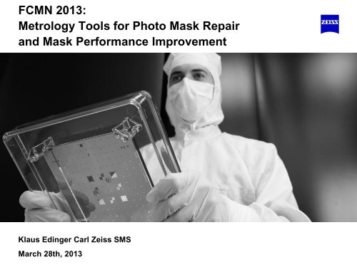
FCMN 2013:<br />
<strong>Metrology</strong> <strong>Tools</strong> <strong>for</strong> <strong>Photo</strong> M<strong>as</strong>k <strong>Repair</strong><br />
<strong>and</strong> M<strong>as</strong>k Per<strong>for</strong>mance Improvement<br />
Klaus Edinger Carl Zeiss SMS<br />
March 28th, 2013
Resolution, "Shrink" (nm)<br />
193<br />
193i<br />
Lithography Roadmap & Key M<strong>as</strong>k Challenges<br />
200<br />
DRAM<br />
Logic<br />
NAND Fl<strong>as</strong>h<br />
OPC M<strong>as</strong>k<br />
100<br />
80<br />
60<br />
50<br />
40<br />
30<br />
20<br />
10<br />
Advanced<br />
<strong>Repair</strong><br />
Technology<br />
Actinic/193nm<br />
<strong>Metrology</strong> &<br />
M<strong>as</strong>k Tuning<br />
AIMS EUV<br />
& advanced<br />
<strong>Repair</strong><br />
EUV DPT<br />
DPT & Overlay<br />
EUV M<strong>as</strong>k Ph<strong>as</strong>e Defect<br />
SEM Image AFM Image<br />
’02 ’03 ’04 ’05 ’06 ’07 ’08 ’09 ’10 ’11 ’12 ’13 ’14 ’15<br />
Year<br />
Carl Zeiss SMS GmbH, Klaus Edinger 03/27/2013<br />
2
Carl Zeiss „Perfect M<strong>as</strong>k Solutions“<br />
Design<br />
Patterning<br />
<strong>Metrology</strong><br />
Tuning<br />
Inspection<br />
<strong>Repair</strong><br />
Verification<br />
Cleaning<br />
In-die <strong>Metrology</strong><br />
Perfect image placement,<br />
CD & ph<strong>as</strong>e me<strong>as</strong>urement<br />
M<strong>as</strong>k Tuning<br />
Improve registration, overlay<br />
<strong>and</strong> CD per<strong>for</strong>mance<br />
Zero Defect Solutions<br />
High precision repair <strong>and</strong><br />
actinic repair verification<br />
PROVE ® RegC ®<br />
MeRiT ®<br />
AIMS<br />
WLCD<br />
CDC<br />
Carl Zeiss SMS GmbH, Klaus Edinger<br />
03/27/2013<br />
3
Motivation<br />
ITRS 2011 – Optical m<strong>as</strong>k requirements<br />
Year 2011 2012 2013 2014 2015 2016<br />
DRAM ½ pitch (nm) 36 32 28 25 23 20<br />
Fl<strong>as</strong>h ½ pitch (nm) 22 20 18 17 15 14<br />
MPU/ASIC Metal 1(M1) ½ pitch (nm) 38 32 27 24 21 19<br />
Generic M<strong>as</strong>k Requirements<br />
M<strong>as</strong>k minimum primary feature size 99 88 80 80 80 80<br />
CDU isolated lines (nm 3S) 2.3 2.1 1.7 1.5 1.2 1.1<br />
CDU dense lines (nm 3S) 3,0 2,4 1.9 1.5 1.3 1.0<br />
Image placement* (S/O removed) 4,3 3.8 3.4 3.0 2.7 2.4<br />
Image placement <strong>for</strong> double patterning*<br />
(S/O removed) ** 3,4 3,0 2,7 2,4 2,1 1,9<br />
* Not including pellicle induced errors<br />
* *ITRS 2010<br />
‣ The current <strong>and</strong> the near future registration specs are very challenging <strong>for</strong> m<strong>as</strong>k manufacturers.<br />
‣ Emph<strong>as</strong>ized with the appearance of the Double Patterning (DP) techniques.<br />
Carl Zeiss SMS GmbH, Klaus Edinger<br />
03/27/2013
PROVE ®<br />
Tool Overview<br />
System electronics<br />
193 nm L<strong>as</strong>er<br />
Horizontal<br />
purge<br />
concept with<br />
separated<br />
zones<br />
Illuminator<br />
<strong>for</strong> reflection<br />
Advanced damping concept<br />
Homogenizer<br />
<strong>and</strong> illuminator<br />
<strong>for</strong> transmission<br />
External h<strong>and</strong>ling<br />
area, (SMIF pod)<br />
Precision stage<br />
Carl Zeiss SMS GmbH, Klaus Edinger<br />
03/27/2013 5
PROVE ®<br />
Schematic optical layout<br />
Autofocus system<br />
CCD camera<br />
Flexible<br />
illumination<br />
<strong>for</strong> transmission or<br />
reflection<br />
Imaging optics<br />
=193nm, NA=0.60<br />
pellicle compatible<br />
Image processing<br />
Auxiliary optics<br />
<strong>for</strong> coarse alignment<br />
Reticle<br />
(face-up)<br />
Stage<br />
actively controlled in 6 dof<br />
ultra precise stage metrology system<br />
Carl Zeiss SMS GmbH, Klaus Edinger<br />
03/27/2013 6
RegC ® Process Concept<br />
‣ De<strong>for</strong>mation of the m<strong>as</strong>k bulk on the level of few PPM’s is done by writing special<br />
de<strong>for</strong>mation elements utilizing ultra short l<strong>as</strong>er pulses.<br />
‣ Calibration of the de<strong>for</strong>mation magnitude <strong>and</strong> direction is done with a special in situ<br />
metrology system that determines the induced de<strong>for</strong>mation properties.<br />
requires<br />
X<br />
expansio<br />
n<br />
FS Pulse - L<strong>as</strong>er<br />
<strong>Metrology</strong><br />
System<br />
Beam Shaper<br />
& Scanner<br />
Focusing<br />
Optics<br />
requires<br />
Y<br />
expansio<br />
n<br />
Carl Zeiss SMS GmbH, Klaus Edinger<br />
03/27/2013
Target of the RegC ® Process<br />
RegC ® target: Bring all registration errors to a correctable systematic field.<br />
Raw Reg error<br />
RegC ® process<br />
Simulated best<br />
correctable error<br />
S/O of best<br />
correctable error<br />
[nm] X Y<br />
[nm] X Y<br />
Abs Max 12.0 1.5<br />
Abs Max 0.1 0.5<br />
3S 7.3 1.5<br />
3S 0.1 0.3<br />
‣ The RegC ® algorithm allows to simulate the best correctable field.<br />
‣ The RegC ® process generates local de<strong>for</strong>mations to compensate <strong>for</strong> local registration errors.<br />
‣ The errors magnitude is incre<strong>as</strong>ed but all are correctable by the scanner.<br />
‣ After scanner S/O removal the residual registration will be minimized.<br />
Carl Zeiss SMS GmbH, Klaus Edinger<br />
03/27/2013
RegC ® CDU Neutral - Process Steps<br />
‣ Utilizing the full m<strong>as</strong>k area, including the exposure field incre<strong>as</strong>es the RegC ® efficiency.<br />
‣ By writing RegC ® with two modes it is possible to maintain a constant attenuation across the<br />
exposure field <strong>and</strong> thereby maintaining CDU.<br />
Step 1 , X - axis<br />
Step 2 , Y - axis<br />
Sum of steps 1&2<br />
+<br />
=<br />
Exposure Field<br />
Fixed light<br />
attenuation<br />
104 X 132 mm<br />
Transmission uni<strong>for</strong>mity in the<br />
exposure field is maintained >><br />
CDU unchanged<br />
Carl Zeiss SMS GmbH, Klaus Edinger<br />
03/27/2013
RegC ® CDU Neutral – Results<br />
Pre RegC ®<br />
Scale/Ortho removed<br />
Post RegC ®<br />
Scale/Ortho removed<br />
Systematic<br />
residuals<br />
Reduced<br />
systematic<br />
residuals<br />
3S (S/O removed)<br />
Pre [nm] Post [nm]<br />
Improvement<br />
X 8.21 4.12 4.09 50 %<br />
Y 8.55 3.95 4.60 54 %<br />
Enables double patterning specifications !!!<br />
Carl Zeiss SMS GmbH, Klaus Edinger<br />
03/27/2013
M<strong>as</strong>k <strong>Metrology</strong>: WLCD – CD <strong>Metrology</strong> b<strong>as</strong>ed<br />
on proven Aerial Image Technology<br />
• WLCD is b<strong>as</strong>ed on proven<br />
Aerial Image Technology<br />
• WLCD me<strong>as</strong>ures under the<br />
same conditions <strong>as</strong> the<br />
scanner<br />
• WLCD captures OPC <strong>and</strong><br />
optical MEEF effects<br />
• Simplifies me<strong>as</strong>urement <strong>for</strong><br />
complex 2D features<br />
• FreeForm Illumination<br />
supports SMO technology<br />
• Applied illumination conditions:<br />
same <strong>as</strong> <strong>for</strong> wafer print<br />
Scanner<br />
0.25x<br />
Illuminator<br />
M<strong>as</strong>k<br />
NA 0.35<br />
NA 1.4<br />
Wafer<br />
Wafer print<br />
Illumination<br />
M<strong>as</strong>k<br />
WLCD<br />
450x<br />
Equivalent image <strong>for</strong>mation <strong>for</strong><br />
Scanner <strong>and</strong> WLCD<br />
Illuminator<br />
M<strong>as</strong>k<br />
NA 0.35<br />
NA ~ 0<br />
CCD Camera<br />
Aerial image<br />
Carl Zeiss SMS GmbH, Klaus Edinger<br />
03/27/2013 11
Carl Zeiss „Perfect M<strong>as</strong>k Solutions“<br />
Design<br />
Patterning<br />
<strong>Metrology</strong><br />
Tuning<br />
Inspection<br />
<strong>Repair</strong><br />
Verification<br />
Cleaning<br />
In-die <strong>Metrology</strong><br />
Perfect image placement,<br />
CD & ph<strong>as</strong>e me<strong>as</strong>urement<br />
M<strong>as</strong>k Tuning<br />
Improve registration, overlay<br />
<strong>and</strong> CD per<strong>for</strong>mance<br />
Zero Defect Solutions<br />
High precision repair <strong>and</strong><br />
actinic repair verification<br />
PROVE ® RegC ®<br />
MeRiT ®<br />
AIMS<br />
WLCD<br />
CDC<br />
Carl Zeiss SMS GmbH, Klaus Edinger<br />
03/27/2013<br />
12
Focused electron beam b<strong>as</strong>ed m<strong>as</strong>k repair<br />
Real defect<br />
<strong>Repair</strong> shape(s)<br />
Computer-<strong>as</strong>sisted shape generation, modification <strong>and</strong> placement<br />
Carl Zeiss SMS GmbH, Klaus Edinger<br />
03/27/2013<br />
13
Electron beam induced deposition <strong>and</strong> etching<br />
Deposition<br />
Etching<br />
Adsorption of precursor molecules:<br />
• Exposure with electron beam<br />
• Reaction <strong>and</strong> immobilization of precursor Deposition<br />
• Reaction with substrate <strong>and</strong> volatilization Etching<br />
Carl Zeiss SMS GmbH, Klaus Edinger<br />
03/27/2013 14
State-of-the-art achievements with the MeRiT<br />
Statistics over 2 months at a<br />
customer‘s site:<br />
• 74% yield on 1 st attempt;<br />
• 24% incre<strong>as</strong>e on further<br />
attempts<br />
MoSi<br />
100 nm<br />
Qz<br />
A. Garetto et al., Proc. SPIE (2009)<br />
Carl Zeiss SMS GmbH, Klaus Edinger<br />
03/27/2013 15
Optical repair qualification by aerial imaging<br />
No wafer stepper in the m<strong>as</strong>k-shop<br />
193 nm CCD exposure with „Aerial<br />
Imaging <strong>Metrology</strong> System“ (AIMS TM )<br />
Detailed ph<strong>as</strong>e & intensity in<strong>for</strong>mation<br />
on 10 x 10 µm are<strong>as</strong><br />
Diffractionlimited<br />
UV<br />
distribution<br />
Carl Zeiss SMS GmbH, Klaus Edinger<br />
03/27/2013 16
AIMS: Process window evaluation<br />
Carl Zeiss SMS GmbH, Klaus Edinger<br />
03/27/2013<br />
17
EUV absorber e-beam repair<br />
25 nm real defects<br />
25 nm real defects After e-beam repair<br />
M<strong>as</strong>k SEM NXE: 3100 M<strong>as</strong>k SEM NXE: 3100 Comment<br />
Complex<br />
OK<br />
Half height<br />
OK<br />
Multiline<br />
OK<br />
<strong>Repair</strong> success on real defects validated on NXE:3100 scanner<br />
Carl Zeiss SMS GmbH, Klaus Edinger<br />
03/27/2013 18
EUV multilayer defect<br />
Cross-sectional profile<br />
Simulated aerial image<br />
Dose to size<br />
Carl Zeiss SMS GmbH, Klaus Edinger<br />
03/27/2013
EUV multilayer defect<br />
Compensational repair simulation<br />
LS pattern with bump<br />
Aerial image<br />
Line<br />
Space<br />
Distorsion<br />
Dose to size<br />
Carl Zeiss SMS GmbH, Klaus Edinger<br />
03/27/2013 20
EUV multilayer defect<br />
Compensational repair simulation<br />
LS pattern with bump<br />
Aerial image<br />
Line<br />
Space<br />
Distorsion<br />
Dose to size<br />
Carl Zeiss SMS GmbH, Klaus Edinger<br />
03/27/2013 21
EUV multilayer defect<br />
Compensational repair simulation<br />
LS pattern with bump<br />
Aerial image<br />
Line<br />
Space<br />
Distorsion<br />
Dose to size<br />
Carl Zeiss SMS GmbH, Klaus Edinger<br />
03/27/2013 22
EUV multilayer defect<br />
Compensational repair simulation<br />
LS pattern with bump<br />
Aerial image<br />
Line<br />
Space<br />
Distorsion<br />
Dose to size<br />
Carl Zeiss SMS GmbH, Klaus Edinger<br />
03/27/2013 23
EUV multilayer defect<br />
Compensational repair simulation<br />
LS pattern with bump<br />
Aerial image<br />
Line<br />
Space<br />
Distorsion<br />
Dose to size<br />
Carl Zeiss SMS GmbH, Klaus Edinger<br />
03/27/2013 24
EUV multilayer defect<br />
Compensational repair simulation<br />
LS pattern with bump<br />
Aerial image<br />
Line<br />
Space<br />
Distorsion<br />
Dose to size<br />
Carl Zeiss SMS GmbH, Klaus Edinger<br />
03/27/2013 25
EUV multilayer defect<br />
Compensational repair simulation<br />
LS pattern with bump<br />
Aerial image<br />
Line<br />
Space<br />
Distorsion<br />
Note: Printability of ML defects is strongly focus dependent<br />
Dose to size<br />
Carl Zeiss SMS GmbH, Klaus Edinger<br />
03/27/2013 26
EUV multilayer defect<br />
ML bump: reticle cross-section<br />
Simulated aerial image<br />
SEM<br />
AFM<br />
SEM<br />
AFM<br />
5 nm „bump 3 nm „pit“<br />
Problem: Many mirror distortions that print are invisible in SEM!<br />
Carl Zeiss SMS GmbH, Klaus Edinger 03/27/2013<br />
27
EUV multilayer defect:<br />
Detection by integrated AFM<br />
ML bump: reticle cross-section<br />
Simulated aerial image<br />
SEM<br />
AFM<br />
SEM<br />
AFM<br />
3 nm „bump 5 nm „pit“<br />
But: All ML defects found so far by wafer printing could be<br />
successfully visualized by AFM!<br />
Carl Zeiss SMS GmbH, Klaus Edinger 03/27/2013<br />
28
Integrated AFM system<br />
- Dual head AFM system<br />
- F<strong>as</strong>ter turnaround since<br />
m<strong>as</strong>k stays in vacuum<br />
- Closed loop with repair<br />
software<br />
- Automated tip exchange system<br />
- Tip exchange < 120 min<br />
- Applications<br />
- F<strong>as</strong>t process tuning<br />
- 3D defect repair shape<br />
generation<br />
- EUV compensational repair<br />
AFM<br />
AFM<br />
Column<br />
Stage<br />
Main Body<br />
Carl Zeiss SMS GmbH, Klaus Edinger<br />
03/27/2013 29
Compensational repair:<br />
“Bump defect”<br />
AFM: 3 nm „bump“ Compensated SEM<br />
Wafer<br />
be<strong>for</strong>e<br />
repair<br />
BF -100 nm BF -50 nm BF BF +50 nm BF +100 nm<br />
Wafer<br />
after<br />
repair<br />
40 nm HP per<strong>for</strong>med on the ASML Alpha Demo Tool<br />
Carl Zeiss SMS GmbH, Klaus Edinger<br />
03/27/2013<br />
30
Compensational repair:<br />
„Pit defect“<br />
AFM: 3 nm pit Compensated SEM<br />
BF -100 nm BF -50 nm BF BF +50 nm BF +100 nm<br />
Propagating<br />
ML pit simulation<br />
Carl Zeiss SMS GmbH, Klaus Edinger<br />
Through-focus ML pit compensation repair<br />
(see R. Jonckheere et al., Proc. SPIE 8166, 81661G (2011))<br />
03/27/2013 31
Summary<br />
• The extension of optical lithography h<strong>as</strong> strongly incre<strong>as</strong>ed the dem<strong>and</strong>s on<br />
advanced photo m<strong>as</strong>ks<br />
• Carl Zeiss SMS h<strong>as</strong> developed dedicated tools sets to improve photo m<strong>as</strong>k<br />
registration, overlay <strong>and</strong> CD uni<strong>for</strong>mity b<strong>as</strong>ed on femto second l<strong>as</strong>er writing<br />
in two closed loop applications with registration <strong>and</strong> wafer level CD<br />
me<strong>as</strong>urements.<br />
• MeRiT ® e-beam m<strong>as</strong>k repair ready <strong>for</strong> 32 nm, 27nm <strong>and</strong> 25nm EUV<br />
absorber defects<br />
• MeRiT ® e-beam m<strong>as</strong>k repair is capable <strong>for</strong> ML defect repair utilizing data of<br />
an integrated AFM <strong>for</strong> placement <strong>and</strong> compensational shape generation<br />
• Compensational repair h<strong>as</strong> its limits. Defect reduction during blank<br />
manufacturing is strongly recommended<br />
Carl Zeiss SMS GmbH, Klaus Edinger<br />
03/27/2013 32
Carl Zeiss SMS GmbH, Klaus Edinger<br />
03/27/2013