Surface and bulk passivation of multicrystalline silicon solar cells by ...
Surface and bulk passivation of multicrystalline silicon solar cells by ... Surface and bulk passivation of multicrystalline silicon solar cells by ...
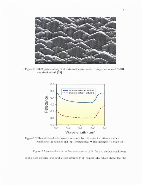
21 Figure 2.1 SEM picture of a typical texturized silicon surface using conventional NaOH texturization bath [39]. Figure 2.2 The calculated reflectance spectra of a bare Si wafer for different surface conditions: (a) polished and (b) (100) textured. Wafer thickness =300 μm [40]. Figure 2.2 summarizes the reflectance spectra of Si for two surface conditions: double-side polished and double-side textured [40], respectively, which shows that the
22 reflectance of polished Si can be greatly lowered by texturing. For a well-textured surface of a (100)-oriented wafer, the reflectance can be as low as 0.1. The other approach is to deposit thin coatings of a material on top of the surface of a photovoltaic cell that reduces the light reflection and increases light transmission. These coatings are called antireflection (AR) coatings. The materials include SiO2, 1'iO2, ΖnO2, MgF and Si3N4. A single layer of the antireflection material is usually several hundred nanometers thick. The most common method for broadbanding in optical applications is to use multilayer coatings that exhibit reflectance nulls at several wavelengths [41]. If the nulls are located close to each other, it can result in a very low reflectance surface. This approach has been successfully applied in other optical devices, such as beam splitters, architectural glass windows, and optical instruments. But, because of cost considerations, a conventional multilayer approach is not suitable for solar cells. However, the broadband anti-reflection features in solar cells are obtained through the use of rough surfaces, in conjunction with a single-layer of AR coating. In the past, the PV industry has used materials, such as SίO2 and TiO2 for AR coatings. SίO2 is not an ideal material for AR coating of Si because its refractive index (n=1.45) is too low. However, it offers the advantage of providing surface passivation. On the other hand, TiO2 is better matched optically with Si, but does not contribute to surface passivation. SIN offers a better match as an AR coating for Si, but the cost of depositing nitride layers is generally high and is not warranted for low-cost solar cells. However, the nitridation process can save other process steps and contribute to significant improvement of the cell efficiency, making it a viable option [42].
- Page 1 and 2: Copyright Warning & Restrictions Th
- Page 3 and 4: ABSTRACT SURFACE AND BULK PASSIVATI
- Page 5 and 6: SURFACE AND BULK PASSIVATION OF MUL
- Page 7 and 8: APPROVAL PAGE SURFACE AND BULK PASS
- Page 9 and 10: Chuan Li, B.L. Sopori, P. Rupnowski
- Page 11 and 12: ACKNOWLEDGEMENT The work presented
- Page 13 and 14: TABLE OF CONTENTS (Continued) Chapt
- Page 15 and 16: LIST OF TABLES Table Page 2.1 Posit
- Page 17 and 18: LIST OF FIGURES (Continued) Figure
- Page 19 and 20: LIST OF FIGURES (Continued) Figure
- Page 21 and 22: 2 percent; however, soon, more adva
- Page 23 and 24: 4 Figure 1.1 World solar module pro
- Page 25 and 26: 6 bond is called a hole. It too can
- Page 27 and 28: 8 Figure 1.4 The I-V characteristic
- Page 29 and 30: 10 First generation cells consist o
- Page 31 and 32: 12 Basically, materials for manufac
- Page 33 and 34: 14 Defects are generally categorize
- Page 35 and 36: 16 copper, or nickel in concentrati
- Page 37 and 38: 18 the SiNx:H layer during the ther
- Page 39: CHAPTER 2 SILICON NITRIDE LAYER FOR
- Page 43 and 44: 24 information is application-orien
- Page 45 and 46: 26 film fed growth (EFG) ribbon sil
- Page 47 and 48: 28 Figure 2.5 Deposition of SiΝ :
- Page 49 and 50: 30 Figure 2.6 shows the dependence
- Page 51 and 52: 32 atoms, the interface states are
- Page 53 and 54: 34 2.5 Bulk Passivation of Si by Si
- Page 55 and 56: 36 It was found that the bulk lifet
- Page 57 and 58: CHAPTER 3 MODELING OF SURFACE RECOM
- Page 59 and 60: 40 Figure 3.2 Schematic diagram of
- Page 61 and 62: 42 σ and σp are the capture cross
- Page 63 and 64: 44 Qsi — charge density induced i
- Page 66 and 67: 47 Figure 3.5 The calculated depend
- Page 68 and 69: 49 * 10 Λ m; m is in a range from
- Page 70 and 71: 51 Na, sigma_n, sigma_p: enter x.xx
- Page 72 and 73: 53 Figure 3.7 Measured Seff(Δn) de
- Page 74 and 75: 55 curves converge to a single valu
- Page 76 and 77: 57 seen that, initially Ss decrease
- Page 78 and 79: 59 carrier recombination within the
- Page 80 and 81: 61 recombination in the SCR influen
- Page 82 and 83: 63 Figure 3.13 shows that: 1) after
- Page 84 and 85: CHAPTER 4 MINORITY-CARRIER LIFETIME
- Page 86 and 87: 67 Figure 4.1 Α photograph of QSSP
- Page 88 and 89: 69 work. The most convenient is 1 m
21<br />
Figure 2.1 SEM picture <strong>of</strong> a typical texturized <strong>silicon</strong> surface using conventional NaOH<br />
texturization bath [39].<br />
Figure 2.2 The calculated reflectance spectra <strong>of</strong> a bare Si wafer for different surface<br />
conditions: (a) polished <strong>and</strong> (b) (100) textured. Wafer thickness =300 μm [40].<br />
Figure 2.2 summarizes the reflectance spectra <strong>of</strong> Si for two surface conditions:<br />
double-side polished <strong>and</strong> double-side textured [40], respectively, which shows that the


