Surface and bulk passivation of multicrystalline silicon solar cells by ...
Surface and bulk passivation of multicrystalline silicon solar cells by ... Surface and bulk passivation of multicrystalline silicon solar cells by ...
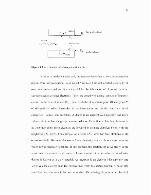
5 Figure 1.2 A schematic of photogeneration effect. In order to produce a solar cell, the semiconductor has to be contaminated or doped. Pure semiconductors (also called "intrinsic") do not conduct electricity at room temperature and are thus not useful for the fabrication of electronic devices. Semiconductors conduct electricity if they are doped with a small amount of impurity atoms. In the case of silicon (Si), these would be atoms from group III and group V of the periodic table. Impurities in semiconductors are divided into two broad categories: donors and acceptors. A donor is an element with typically one more valence electron than the group IV semiconductor. Each Si atom has four electrons in its outermost shell; these electrons are involved in forming chemical bonds with the neighboring Si atoms. For example, an arsenic (As) atom has five electrons in its outermost shell. The extra electron in As can be easily removed from the As donor on which it was originally localized. If this happens, the electron can move freely in the semiconductor material and conduct electric current. A semiconductor doped with donors is known as n-type material. An acceptor is an element with typically one fewer valence electron than the element that forms the semiconductor. A boron (B) atom has three electrons in its outermost shell. The missing electron in the chemical
6 bond is called a hole. It too can be easily removed from the vicinity of the B atom and move freely in the semiconductor material. A semiconductor doped with acceptors is known as p-type material. As the two types of semiconductors are brought together, a p-n junction is formed and the concentration gradient of carriers near the metallurgical junction leads to a carrier flow. As the junction region gets "depleted" of carriers, the ionized dopant cores left behind build up an electric field across the junction, which introduces drift current that is opposite to the diffusion current. An equilibrium situation will be arrived at as the two currents match. In the dark, the equilibrated p-n junction should have a spatially uniform Fermi level and no net macroscopic current flow is observed. When a p-n junction is illuminated, excess electron-hole pairs are generated by light throughout the cell. This disturbs the equilibrium state of carriers everywhere. The excess electrons (holes) in n-type (p-type) region diffuse towards the junction and are quickly pulled across the depletion region by the electric field. This is the photovoltaic effect. A simplified solar cell model is usually illustrated as a current source in parallel with a diode and, a shunt resistance and a series resistance component as well are added. The resulting equivalent circuit of a solar cell is shown in Figure 1.3. Notice that the current generated by the photons is represented by an independent source. The two resistors shown in Figure 1.3 represent two of the losses in a solar cell. Rs is a series resistance loss due, primarily, to the ohmic loss in the surface of the solar cell. The shunt resistance, Rsh, is used to model leakage currents. A shunt resistance of a few hundred ohms does not reduce the output power of the solar cell appreciably. In reality, Rsh is much larger than a few hundred ohms and can in most
- Page 1 and 2: Copyright Warning & Restrictions Th
- Page 3 and 4: ABSTRACT SURFACE AND BULK PASSIVATI
- Page 5 and 6: SURFACE AND BULK PASSIVATION OF MUL
- Page 7 and 8: APPROVAL PAGE SURFACE AND BULK PASS
- Page 9 and 10: Chuan Li, B.L. Sopori, P. Rupnowski
- Page 11 and 12: ACKNOWLEDGEMENT The work presented
- Page 13 and 14: TABLE OF CONTENTS (Continued) Chapt
- Page 15 and 16: LIST OF TABLES Table Page 2.1 Posit
- Page 17 and 18: LIST OF FIGURES (Continued) Figure
- Page 19 and 20: LIST OF FIGURES (Continued) Figure
- Page 21 and 22: 2 percent; however, soon, more adva
- Page 23: 4 Figure 1.1 World solar module pro
- Page 27 and 28: 8 Figure 1.4 The I-V characteristic
- Page 29 and 30: 10 First generation cells consist o
- Page 31 and 32: 12 Basically, materials for manufac
- Page 33 and 34: 14 Defects are generally categorize
- Page 35 and 36: 16 copper, or nickel in concentrati
- Page 37 and 38: 18 the SiNx:H layer during the ther
- Page 39 and 40: CHAPTER 2 SILICON NITRIDE LAYER FOR
- Page 41 and 42: 22 reflectance of polished Si can b
- Page 43 and 44: 24 information is application-orien
- Page 45 and 46: 26 film fed growth (EFG) ribbon sil
- Page 47 and 48: 28 Figure 2.5 Deposition of SiΝ :
- Page 49 and 50: 30 Figure 2.6 shows the dependence
- Page 51 and 52: 32 atoms, the interface states are
- Page 53 and 54: 34 2.5 Bulk Passivation of Si by Si
- Page 55 and 56: 36 It was found that the bulk lifet
- Page 57 and 58: CHAPTER 3 MODELING OF SURFACE RECOM
- Page 59 and 60: 40 Figure 3.2 Schematic diagram of
- Page 61 and 62: 42 σ and σp are the capture cross
- Page 63 and 64: 44 Qsi — charge density induced i
- Page 66 and 67: 47 Figure 3.5 The calculated depend
- Page 68 and 69: 49 * 10 Λ m; m is in a range from
- Page 70 and 71: 51 Na, sigma_n, sigma_p: enter x.xx
- Page 72 and 73: 53 Figure 3.7 Measured Seff(Δn) de
5<br />
Figure 1.2 A schematic <strong>of</strong> photogeneration effect.<br />
In order to produce a <strong>solar</strong> cell, the semiconductor has to be contaminated or<br />
doped. Pure semiconductors (also called "intrinsic") do not conduct electricity at<br />
room temperature <strong>and</strong> are thus not useful for the fabrication <strong>of</strong> electronic devices.<br />
Semiconductors conduct electricity if they are doped with a small amount <strong>of</strong> impurity<br />
atoms. In the case <strong>of</strong> <strong>silicon</strong> (Si), these would be atoms from group III <strong>and</strong> group V<br />
<strong>of</strong> the periodic table. Impurities in semiconductors are divided into two broad<br />
categories: donors <strong>and</strong> acceptors. A donor is an element with typically one more<br />
valence electron than the group IV semiconductor. Each Si atom has four electrons in<br />
its outermost shell; these electrons are involved in forming chemical bonds with the<br />
neighboring Si atoms. For example, an arsenic (As) atom has five electrons in its<br />
outermost shell. The extra electron in As can be easily removed from the As donor on<br />
which it was originally localized. If this happens, the electron can move freely in the<br />
semiconductor material <strong>and</strong> conduct electric current. A semiconductor doped with<br />
donors is known as n-type material. An acceptor is an element with typically one<br />
fewer valence electron than the element that forms the semiconductor. A boron (B)<br />
atom has three electrons in its outermost shell. The missing electron in the chemical


