Dielectric Aluminum Oxides: Nano-Structural Features and ...
Dielectric Aluminum Oxides: Nano-Structural Features and ...
Dielectric Aluminum Oxides: Nano-Structural Features and ...

You also want an ePaper? Increase the reach of your titles
YUMPU automatically turns print PDFs into web optimized ePapers that Google loves.
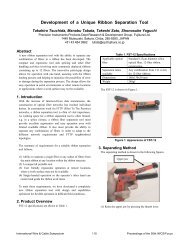
The surfaces of various films on Al substrates were observed with a Hitachi FE-4800. An<br />
electron beam with 1.5 keV acceleration voltage <strong>and</strong> 7-10 µA current was used for imaging.<br />
Working distance was kept at ~ 1.5 mm while both SE detectors were mixed for better detail.<br />
Prior to the FE-SEM analysis, all films were coated with a 2 nm Pt/Pd layer from a 208<br />
HR/MTM20 Cressington Sputter unit.<br />
Specimens to be examined by TEM were thinned using a Hitachi FB2000A focused ion<br />
beam (FIB). A beam of Ga ions radiating parallel to the plane of the sample face was used to<br />
cut sections of ~ 50 nm thickness. These thin sections of the oxide films on Al substrate were<br />
examined with a Hitachi HD-2300 TEM. A beam with 200 kV acceleration voltage <strong>and</strong> 20-<br />
30 µA current was used for imaging. Electron diffraction patterns were generated using a<br />
beam diameter of 200-300 nm at 200 kV <strong>and</strong> 80-85 nA current.<br />
Stability Testing was accomplished by using a ramp-build-time test in 85 °C citric acid<br />
solution with 0.5 mA/cm2 current density after boiling for two hours in deionized (DI)-<br />
water. The rise times to 95% of V f were measured <strong>and</strong> used to assess the stability of the<br />
grown oxides, <strong>and</strong>, in turn, the level of defects/voids exposed by boiling.<br />
Anodization of Etched Foil:<br />
RESULTS<br />
One of the accepted methods of producing amorphous aluminum oxide for high voltage use<br />
involves initially anodizing the etched foil at low temperature in an oxidizing acid such as<br />
sulfuric acid to deposit a thick amorphous, porous layer of alumina inside the etch structure.<br />
Figures 1 <strong>and</strong> 2 show a plan view <strong>and</strong> a cross-sectional view of such porous oxides inside of<br />
etch tunnels. While this oxide has little in the way of barrier properties, it serves as the base<br />
layer for a formation step which fills in the pores with additional amorphous oxide to leave a<br />
barrier layer of the desired forming voltage. This oxide has the ability to withst<strong>and</strong> high<br />
duty cycles of charge – discharge with minimal increases in leakage current <strong>and</strong> dissipation<br />
factor. Unfortunately, amorphous oxide has a higher dielectric ratio [~1.4 nm/V] as<br />
compared to crystalline aluminum oxide [~1.0nm/V] which leads to 40% lower capacitance.<br />
The disadvantage of crystalline oxide is the presence of appreciable tensile stress which may<br />
lead to relaxation <strong>and</strong> cracking when subjected to thermal, chemical, electrical or mechanical<br />
stressors. The 40% capacitance advantage of crystalline oxide explains why so much work<br />
has gone into stabilization of the crystalline oxide on capacitor foils.<br />
64