<strong>Spectrum</strong> <strong>Digital</strong>, Inc Table 1: C5515 GPIO Terminal Functions C5515 Pin # C5515 Default Multiplexed Function GPIO Pin Routed To P11 LCD_DATA9 GP[19] N11 LCD_DATA10 GP[20] LCD_DATA9 = I2S2_FS, SH19, U12-3 LCD_DATA9 = SPI_CS0, SH17, U9-1 LCD_DATA9 = SPI_CS0, SH18, J13-7 LCD_DATA9 = I2S2_FS, SH19, U12-3 LCD_DATA10 = I2S2_RX, SG 19, U12-5 LCD_DATA10 = SPI_RX, SH17, U9-2 LCD_DATA10 = SPI_RX, SH18, J13-13 LCD_DATA10 = I2S2_RX, SH19, U12-5 P12 LCD_DATA11 GP[27] LCD_DATA11 = I2S2_DX, SH19, U12-4 LCD_DATA11 = SPI_DX, SH17, U9-5 LCD_DATA11 = SPI_DX, SH18, J13-11 LCD_DATA11 = I2S2_DX, SH19, U12-4 N12 LCD_DATA12 GP[28] LCD_DATA12 = UART_RTS, SH5, P1-3 LCD_DATA12 = UART_RTX, SH17, U5-12 P13 LCD_DATA13 GP[29] LCD_DATA13 = UART_CTS, SH5, P2-18 LCD_DATA12 = UART_CTS, SH 17, U5-10 N13 LCD_DATA14 GP[30] LCD_DATA14 = UART_RX, SH5, P1-7 LCD_DATA14 = UART_RX, SH17, U5-15 P14 LCD_DATA15 GP[31] LCD_DATA15 = UART_TX, SH5, P1-9 LCD_DATA15 = UART_TX, SH17, U5-13 N3 LCD_EN_RDB SPIO_CLK LCD_EN_RDB = LCD_RE, SH20, J19-15 LCD_EN_RDB = LCD_RE = SPI_ALT_CLK, SH5, P1-16 P4 LCD_CS0_E0 SPI_CS0 LCD_CS0_E0 = LCD_BIAS_OE, SH20, J19-19 N4 LCD_CS1_E1 SPI_CS1 LCD_CS1_E1 = LCD_MCLK = SPI_ALT_CS1, SH5, P1-14 P5 LCD_RW_WRB SPI_CS2 LCD_RW_WRB = LCD_nWE, SH20, J19-16 N5 LCD_RS SPI_CS3 LCD_RS = LCD_ALE, SH20, J19-20 1-6 <strong>TMS320C5515</strong> <strong>EVM</strong> Technical Reference
<strong>Spectrum</strong> <strong>Digital</strong>, Inc 1.5 C5515 <strong>EVM</strong> Memory Map The C5515 <strong>EVM</strong> supports on chip DARAM, off chip SDRAM, off chip NOR flash, and off chip NAND Flash. The addressing for each of these memory blocks is shown in the figure below. CPU Byte Address 000000h 0000C0h 010000h MEMORY BLOCKS (MMR Reserved) Internal DARAM Internal DARAM 050000h 800000h C00000h E00000h F00000h FE0000h ROM (if MPNMC=0) Mobile SDRAM External-CS0 Space NOR Flash External-CS2 Space Not Used External-CS3 Space NAND Flash External-CS4 Space Not Used External-CS5 Space External-CS5 Space (if MPNMC=1) FFFFFFh Figure 1-2, <strong>EVM</strong> C5515 Memory Map 1-7
- Page 1: TMS320C5515 Evaluation Module (EVM)
- Page 4 and 5: IMPORTANT NOTICE Spectrum Digital,
- Page 6 and 7: 2.4 C5515 EVM Switches . . . . . .
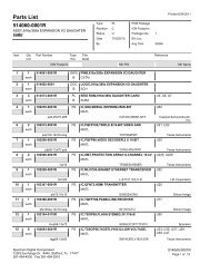
- Page 8 and 9: Table 1: Hardware History Revision
- Page 10 and 11: Spectrum Digital, Inc 1.1 Key Featu
- Page 12 and 13: Spectrum Digital, Inc 1.4 C5515 GPI
- Page 16 and 17: Spectrum Digital, Inc 1.6 C5515 I 2
- Page 18 and 19: Spectrum Digital, Inc Topic Page 2.
- Page 20 and 21: Spectrum Digital, Inc Figure 2-2 sh
- Page 22 and 23: Spectrum Digital, Inc 2.2.1 J1, RS-
- Page 24 and 25: Spectrum Digital, Inc 2.2.4 J4, Hea
- Page 26 and 27: Spectrum Digital, Inc 2.2.8 J8, Ext
- Page 28 and 29: Spectrum Digital, Inc 2.2.12 J12, S
- Page 30 and 31: Spectrum Digital, Inc 2.2.15 J15, M
- Page 32 and 33: Spectrum Digital, Inc 2.2.18 J19, D
- Page 34 and 35: Spectrum Digital, Inc 2.2.21.2 P2,
- Page 36 and 37: Spectrum Digital, Inc 2.4.3 SW4, LD
- Page 38 and 39: Spectrum Digital, Inc 2.5 Jumpers T
- Page 40 and 41: Spectrum Digital, Inc The factory i
- Page 42 and 43: Spectrum Digital, Inc 2.5.1.3 JP5,
- Page 44 and 45: Spectrum Digital, Inc 2.5.1.7 JP39,
- Page 46 and 47: Spectrum Digital, Inc The remaining
- Page 48 and 49: Spectrum Digital, Inc Figure below
- Page 50 and 51: Spectrum Digital, Inc The table bel
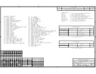
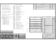
- Page 52 and 53: 1 2 4 5 5 6 7 8 9 A A 4 4 3 3 A 2 2
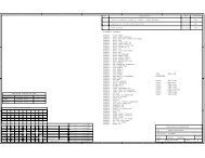
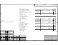
- Page 54 and 55: 1 2 3 4 5 1 2 3 4 5 Spectrum Digita
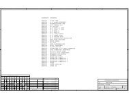
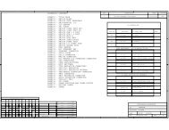
- Page 56 and 57: 5 5 4 4 3 3 2 2 1 1 Spectrum Digita
- Page 58 and 59: 5 5 4 4 3 3 2 2 1 1 Spectrum Digita
- Page 60 and 61: 5 5 4 4 3 3 2 2 1 1 Spectrum Digita
- Page 62 and 63: 5 5 4 4 3 3 2 2 1 1 Spectrum Digita
- Page 64 and 65:
5 5 4 4 3 3 2 2 1 1 Spectrum Digita
- Page 66 and 67:
5 5 4 4 3 3 2 2 1 1 Spectrum Digita
- Page 68 and 69:
5 5 4 4 3 3 2 2 1 1 Spectrum Digita
- Page 70 and 71:
5 5 + 0 4 4 3 3 0 0 2 2 0 0 0 0 1 1
- Page 72 and 73:
Spectrum Digital, Inc A-22 TMS320C5
- Page 74:
Spectrum Digital, Inc THIS DRAWING