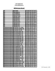
Assembly Induced Defects - AVX
Assembly Induced Defects - AVX
Assembly Induced Defects - AVX

You also want an ePaper? Increase the reach of your titles
YUMPU automatically turns print PDFs into web optimized ePapers that Google loves.
TECHNICAL<br />
INFORMATION<br />
ASSEMBLY INDUCED DEFECTS<br />
by John Maxwell<br />
<strong>AVX</strong> Corporation<br />
Abstract:<br />
Surface mount technology holds many benefits<br />
but there is no room for sloppy practices; SMT<br />
assemblies need the control that semiconductor<br />
processing uses. Extreme care must be taken at<br />
the start of a design to identify all stress zones<br />
and orient components to minimize damage.
ASSEMBLY INDUCED DEFECTS<br />
by John Maxwell<br />
<strong>AVX</strong> Corporation<br />
Introduction<br />
The transition from thru-hole manufacturing to surface<br />
mount technology has made one thing crystal clear: surface<br />
mount components and PC boards are easily damaged by<br />
the soldering and assembly process. Multilayer ceramic<br />
capacitors are sensitive components to damage due to their<br />
complex mechanical structure. But experienced users are<br />
now finding out the hard way that PC boards, plastic molded<br />
ICs or transistors, and even solder places stringent<br />
limitations on assembly processing. The entire assembly is<br />
now subjected to the soldering process exposing all<br />
components and the PC board to high temperatures for long<br />
periods of time. Unfortunately some materials, in particular<br />
the plastics used to manufacture SMT components and PC<br />
boards, are not well suited for high temperature processing.<br />
Sources of assembly induced damage fall into two major<br />
categories: thermal and mechanical.<br />
Thermal Damage<br />
Damage to PC boards, plastic molded components, and<br />
solder is primarily thermal in nature while chip capacitor<br />
and resistor damage is mostly due to external mechanical<br />
stress. Thermal shock cracks in ceramic capacitors have<br />
been described in detail as to causes and solutions (1, 2).<br />
Users are now discovering post solder cracks in plastic<br />
IC packages (3), and PC board blistering, measles, or<br />
delamination. The main culprits are moisture absorption by<br />
the plastics and stress due to large differences in the<br />
coefficient of thermal expansion (CTE) of materials used by<br />
the manufacturer of plastic molded components and PC<br />
boards.<br />
When processing temperatures exceed the glass<br />
transition temperature, Tg, of epoxy resins, the CTE can<br />
increase as much as an order of magnitude over room<br />
temperature values further increasing stress.<br />
Common vapor phase or infrared reflow soldering<br />
temperatures are far beyond the boiling point of water or<br />
glass transition temperatures of epoxies used in PC boards<br />
and molding compounds. A user can do very little to<br />
minimize stress due to CTE mismatch other than follow<br />
a supplier’s recommendations on process limitations.<br />
These usually include peak processing temperatures and<br />
maximum rates of change, dwell times, and preconditioning<br />
procedures.<br />
Material preconditioning is used to drive moisture out of<br />
epoxy resins using time and temperature. A common<br />
solution recommended by both suppliers of ICs and PC<br />
boards is to bake both for extended periods of time at 125°C<br />
for 8 to 24 hours. Unfortunately, solderability of components<br />
and PC boards degrades rapidly at these times and<br />
temperatures due to intermetallic consumption of tin in the<br />
solder plating of base metals. Solid state diffusion of tin and<br />
the base metal forms the intermetallic layer needed for<br />
solder joint formation, but once the tin is completely<br />
Table I. CTEs of Typical Components and Substrates<br />
Material<br />
CTE(ppm/ºC)<br />
Chip Capactior 9.5-11.5<br />
Chip Resistor<br />
≈7<br />
Copper 17.6<br />
FR-4 PC Board (X
Typically excessive post solder joint heating occurs at later<br />
steps in the production process such as wave soldering<br />
components to PC boards while using excessive preheat,<br />
hand soldering large components or RF shields, or<br />
“NUKING” boards during rework/repair.<br />
Rework/repair is the most common cause of excessive<br />
solder joint heating. Usually large, hot soldering irons or<br />
overblown hair dryers are used in this process not only<br />
removing the desired parts but also destroying PC land<br />
pattern adhesion and degrading adjacent solder joints.<br />
When excessive heating occurs, premature failure results in<br />
erratic electrical behavior early in the product life.<br />
Sometimes these failures are found during product test if<br />
thermal cycling is performed, but the majority of failed<br />
solder joints are found by customers. Fractures in fatigued<br />
solder joints occur in high stress zones and are due to<br />
differences in CTE, component length, and temperature<br />
excursions. Figure 1 shows typical solder joint stress zones<br />
for chip components and PLCC IC packages. Other SMT<br />
components such as SOICs (small outline IC), quad chip<br />
carriers, SOTs (small outline transistor), inductors, and<br />
tantalum capacitors all have similar joint stress zones.<br />
Figure 2. Linear Displacement for Different Substrate<br />
Conditions<br />
by design so their installation does not degrade reliability.<br />
In particular, large IC packages need to be isolated from<br />
excessive heat because a solder joint failure will usually<br />
crash the system, but the loss of a chip capacitor or resistor<br />
may not. Adjacent solder joint temperatures must be limited<br />
to less than 125-135ºC or there will be latent failures.<br />
Figure 1. Solder Joint Stress Zones<br />
Longer components have larger solder joint stress during<br />
temperature cycling due to larger linear displacement.<br />
Linear displacement is the difference in length of a<br />
component and the segment of substrate between solder<br />
pads during temperature excursions. Linear displacement is:<br />
∆L = (L) (∆CTE) (∆T), where<br />
L is the initial segment length<br />
∆CTE is the difference in component and<br />
substrate CTE<br />
∆T is the temperature excursion<br />
Figure 2 shows linear displacement for both PC boards<br />
where the CTE is greater than that of a component and a<br />
ceramic substrate where the opposite is true.<br />
Solder joints of large components like IC packages are<br />
the first to fail due to high temperature exposure. Failures<br />
typically occur at package corners which are the highest<br />
stress areas due to large linear displacement. Extreme care<br />
must be taken during all rework/repair process stages to<br />
minimize adjacent solder joint temperatures. It is not<br />
uncommon to find 80W soldering irons in these areas<br />
because production managers want to get things done<br />
quickly, and speed in soldering requires both high power<br />
and temperature. Some large components require a great<br />
deal of heat to be soldered because of high thermal mass so<br />
they should be physically isolated from other solder joints<br />
Mechanical Damage<br />
The old pat answer that all cracks are due to thermal<br />
shock is no longer true for ceramic capacitors and resistors,<br />
as pick and place machine damage and post solder assembly<br />
handling are now the major sources of induced damage.<br />
Thermal shock can and does occur, but only when parts are<br />
wave soldered with little or no preheat or “NUKED” with<br />
large soldering irons during repair/rework procedures.<br />
From 1983 to 1988, pick and place machines were the<br />
dominant source of induced damage with thermal shock and<br />
post solder handling making up the balance. Since 1988,<br />
there has been a shift to post soldering damage as the<br />
primary induced source due to improvements in three areas.<br />
Capacitors have improved, both wave solder users and<br />
equipment vendors recognize the importance of proper<br />
preheat, and there have been advances in pick and place<br />
machine component alignment mechanisms. All induced<br />
defect sources may be present at one time along with the<br />
possibility of defective components masking those sources.<br />
With the exception of placement damage, thermal shock<br />
and post soldering damage will cluster in specific areas on<br />
an assembly. Unfortunately placement damage like<br />
defective incoming parts are randomly distributed across<br />
the board requiring detailed failure analysis including DPA<br />
(destructive physical analysis). Each source of damage has a<br />
unique crack signature that helps identify the cause helping<br />
manufacturing to eliminate those defect sources. Pick and<br />
place machine and post solder handling damage are the<br />
major defect sources facing users today and will be covered<br />
as separate topics.
Pick and Place Machine Damage<br />
Placement damage falls into three categories: top<br />
mechanical alignment or centering, bottom centering, and<br />
placement cracks. Bottom centering is the least common<br />
type of damage today for two main reasons. First, the centering<br />
jaws are low mass and do not impact parts as hard as do<br />
high mass top centering jaw machines. Second, paper tape<br />
packaging has improved or been replaced with plastic<br />
embossed carrier tape minimizing debris in the centering<br />
jaws and associated misalignment damage. Only vacuum<br />
pick-up bit and top mechanical centering will be discussed.<br />
Vacuum Pick-up Bit Damage. Damage or cracks<br />
caused by vacuum pick-up bits is straightforward but<br />
perhaps not quite so obvious. This type of damage is caused<br />
by excessive Z-axis placement force of the vacuum pick-up<br />
bit during component placement and consists of damage<br />
typically just below the surface. In the case of MLCs the<br />
damage typically occurs at the ceramic cover layer/<br />
electrode interface on the chip interior, and from the top<br />
surface it looks like the ceramic is disturbed in a circularor<br />
halfmoon-shaped area. Most ceramics used in making<br />
MLCs are translucent so cracks 5 mils or so below the<br />
surface can look like an impression. In some cases there will<br />
be surface fractures but this has become less common.<br />
Another manifestation of bit damage occurs where solder<br />
paste is on boards supporting parts only on their<br />
terminations. Tensile rupture cracks may be found on the<br />
component bottom or board side running from side to side<br />
in the middle of the part, These internal or surface cracks<br />
lead to excessive leakage currents and capacitor failure.<br />
Chip resistors receive similar damage but surface chip<br />
outs or cracks in the resistive element will result in erratic<br />
resistor values. Time and power/temperature cycling are<br />
needed to promote failure. Figure 3 shows placement bit<br />
damage for both chip capacitors and resistors.<br />
Placement bit damage is the result of excessive<br />
placement force because of improper machine maintenance,<br />
set-up, or equipment failure. Plant air pressure variations,<br />
force monitoring on a daily or shift basis because of the<br />
possibility of force sensor failure. When in line monitors are<br />
used, machines are set up the same way insuring consistent<br />
assembly quality. It’s best to eliminate problems in the<br />
production line by process control.<br />
Top Centering Jaw Damage. Top centering jaw pick<br />
and place machines use alignment jaws or tweezers as part<br />
of the pick-up mechanism such that the part is centered<br />
when plucked from the component carrier (embossed tape,<br />
etc.) or during travel to the placement location. Capacitors,<br />
resistors, transistors, and integrated circuits all require<br />
different sizes of jaws and centering forces for optimum<br />
placement. Unfortunately production requirements may not<br />
allow jaw changes, forcing a compromise where a single jaw<br />
set is adjusted to accommodate large ICs, subjecting smaller<br />
parts to excessive forces. Not only are high forces present<br />
but most centering jaws have small widths, especially on the<br />
ends, increasing alignment stress. Transistor and integrated<br />
circuit plastic bodies are used for alignment instead of the<br />
leads to minimize lead bending, concentrating stress into<br />
the top 10-20 mils of small parts. MLC capacitors have a<br />
tensile strength of ≈10,000 psi and a compressive rupture<br />
strength of ≈15,000 psi. These numbers seem high until we<br />
realize that a phonograph stylus exerts similar forces on<br />
vinyl records. The actual gram force or pound force exerted<br />
by centering jaws must be minimized to eliminate these<br />
defects. Figure 4 shows force concentrations due to<br />
mechanical centering jaws. Figure 5 shows typical visible<br />
top centering jaw cracks.<br />
Figure 4. Component Top View of Centering Jaw Force<br />
Concentration<br />
Figure 3. Common Placement Bit Damage<br />
dirt or water in air lines, and age make it difficult to maintain<br />
consistent placement force. It is uncommon to find two<br />
pneumatic driven pick and place machines with the same<br />
pressure settings within the same facility. Placement force<br />
or pressure is a process parameter that needs to be<br />
monitored on a by-shift, by-machine basis. Machines with<br />
programmable placement pressure also require placement<br />
Figure 5. Resulting Visible Top Surface Cracks
Most induced damage from any source is not visible but<br />
is in the interior of the part or hiding under the termination.<br />
It’s not uncommon to find 90-95% of the damage hidden from<br />
view so when the visible cracks disappear the job is not<br />
done. Impact fractures are typically located 10-15 mils from<br />
the top surface hidden under the termination as shown in<br />
Figure 6.<br />
This type of internal crack does not fail quickly because<br />
there are no cracks that propagate to the surface which<br />
allows entry of external contaminants such as moisture or<br />
flux. It has been shown by Brannon, et al. (8) that<br />
atmospheric moisture and DC voltage are all that is required<br />
to initiate the onset of leakage current in MLCs. Water<br />
hydrolyzes at DC voltages above 0.87V providing an<br />
electrolyte needed for current conduction which occurs very<br />
quickly, causing a failure. Internal cracks require metal<br />
dendritic growth or precipitation between electrodes taking<br />
some time before the onset of leakage failures.<br />
There is a very insidious form of internal damage that<br />
manifests itself as a single inter-electrode crack between<br />
only two or three electrodes that is initiated during<br />
centering. Figure 7 shows this type of crack and<br />
exaggerated ceramic distortion during impact. Again these<br />
cracks exist 10-15 mils below the top surface, right along the<br />
impact plane of the end centering jaw, and 5-15 mils from<br />
the termination.<br />
Figure 6. Internal Centering Damage<br />
Figure 7. Inter-Electrode Impact Crack<br />
Centering jaw damage will be with us until mechanical<br />
alignment is replaced with vision systems and computercorrected<br />
placement. Equipment manufacturers and users<br />
have recognized that pick and place machines are a major<br />
source of damage and are taking steps to eliminate it. Post<br />
solder handling will be the major source of induced damage<br />
facing component users in the future.<br />
Post Solder Handling Damage. Post soldering or<br />
uncontrolled warping after soldering is the least recognized<br />
form of induced damage in surface mount assemblies.<br />
Warping or bending occurs at many process steps after<br />
soldering. Board test, component or connector installation,<br />
depanelization or singulation from a mother board, and final<br />
product installation are the most common sources of post<br />
solder cracks. In each case of these cracks, the tensile<br />
strength of the ceramic is exceeded. These cracks do not<br />
need thermal processing such as soldering to propagate but<br />
occur with an audible snap.<br />
Solder joint mass has an effect on when cracks occur.<br />
Large, bulbous solder joints transfer most bending stress to<br />
the component instead of stretching to relieve stress,<br />
making an assembly more sensitive to handling. Allowable<br />
bending of finished assemblies is a specification that cannot<br />
be an extension of thru-hole technology because entire<br />
components are exposed to stress. There are two possible<br />
approaches to board bending specifications: a linear<br />
mils/inch, or a more realistic minimum bend radius (7).<br />
Minimum bend radius allows only a small deflection in<br />
short segments but a great deal of deflection in long<br />
segments. For example, a one-inch long segment can have<br />
no more than 8.4 mils of uniform deflection with a 60- inch<br />
minimum bend radius, and increases to 124 mils for a fourinch<br />
segment. Uniform bend or deflection is where the<br />
board fits smoothly along the radius of a circle. If there are<br />
large rigid-like ICs, transformers, or connectors, then less<br />
deflection is allowed for any given board length. They key to<br />
eliminating warp cracks is to minimize board flexure at all<br />
handling and installation steps after soldering components<br />
into place.<br />
Manufacturing efficiency dictates multi-up or multiple<br />
assembly panels but here lies the single biggest source of<br />
warp cracks. Singulation or depanelization processes can<br />
induce a great deal of stress (board flexure) in components<br />
near board edges and corners. There are many techniques<br />
available to depanel mother boards, some generate<br />
excessive stress. High stress and usable processes are listed<br />
in Tables 2 and 3.<br />
Table 2. High Stress Depanelization Techniques<br />
1) Prescored boards<br />
2) Perforated boards<br />
3) Routing<br />
4) Breakout tabs<br />
5) Shearing including blanking shears<br />
Table 3. Usable Depanelization Techniques<br />
1) Shearing prerouted boards<br />
a) Components must be isolated from<br />
shear tabs<br />
b) Rigid fixturing<br />
c) A very fast process<br />
2) High speed fine tooth saws<br />
a) Limited only to linear cuts<br />
b) Rigid fixturing is mandatory<br />
c) A dust and debris cleaning step is required<br />
d) A medium speed process<br />
3) Diamond wire cutting<br />
a) A dust and debris cleaning step is required<br />
b) A slow process<br />
4) Laser cutting<br />
a) Currently is limited to 0.047"-thick PC boards<br />
due to excessive board edge charring
) Conductive carbon tale cleaning step<br />
is mandatory<br />
c) It’s expensive and slow<br />
5) Water jet<br />
a) Slow<br />
b) Expensive<br />
c) An additional cleaning/drying step is needed<br />
Cracked components from any board warping source all<br />
have the same signatures. There are two basic failure modes<br />
depending on how the board is bent and if solder mask is<br />
present or not. The presence of solder mask between<br />
component pads makes an assembly more sensitive to<br />
handling damage. Coplanar parts like chip capacitors,<br />
resistors, and transistors will solder flush with the pads due<br />
to molten solder surface tension forces. Now the component<br />
body is resting on solder mask which acts as a fulcrum,<br />
increasing component stress. Depending on board warp,<br />
direction, and component orientation, these cracks<br />
propagate to relieve mechanical stress. Cracks initiate at the<br />
ceramic termination interface where ceramic movement is<br />
restricted by the termination and solder fillet. Because<br />
materials fail more readily in the tensile mode, crack<br />
initiation will typically be at maximum tensile stress sites as<br />
shown in Figure 8.<br />
Figure 9(a). Typical Board Warp Cracks<br />
Figure 9(b, c) Typical Warp Cracks<br />
Figure 8. Crack Initiation Sites<br />
Board warp cracks propagate at a 45º angle away from<br />
the initiation site. When DPA is done on failed units, failures<br />
are often confused with thermal shock or pick and place<br />
machine damage. Thermal shock cracks are at the top<br />
surface and usually consist of a single crack. Pick and place<br />
machine damage is typically under the termination with<br />
multiple fractures and warp cracks always originate at the top<br />
or bottom ceramic/termination interface angling in toward<br />
the component end. Figure 9 shows typical fractures in both<br />
capacitors and resistors. Chip resistors pose an interesting<br />
problem in that they are cut from a piece of ceramic resulting<br />
in sharp corners. This makes them more sensitive to<br />
cracking terminations than MLC capacitors which have<br />
rounded corners and edges. There is greater stress<br />
concentration at sharp corners than ones that are rounded<br />
which increases component sensitivity to board warp.<br />
Figure 10. Typical High Stress Zones for Mounting and<br />
Depaneling<br />
There are regions on boards that experience too much<br />
deflection to achieve high yields and reliability. Rigid<br />
components like capacitors, resistors, and transistors need
to be isolated from these flex or warp zones which are<br />
greatest near mounting holes, connectors, pots,<br />
transformers, and other large parts. Board edges or corners<br />
receive the greatest warp or stress during handling and<br />
installation so components should be isolated by at least 200<br />
mils from those areas. Figure 10 shows typical high stress<br />
zones for depanelization and mounting holes. Each<br />
assembly will have different areas to be avoided and in some<br />
cases are so complex that common sense won’t work. Finite<br />
element analysis, FEA, programs are now available for<br />
personal computers and should be used in the initial design<br />
so high stress ‘zones are identified and sensitive<br />
components are isolated before there are production<br />
defects.<br />
Conclusions<br />
Every step in an SMT assembly process can induce<br />
defects. Sub ppm defects demand these potential sources be<br />
identified and eliminated. The tendency to “use a bigger<br />
hammer to make it fit” syndrome will only damage SMT<br />
assemblies. Force fitting a process or boards will only<br />
damage components, causing field failures. Surface mount<br />
technology holds many benefits but there is no room for<br />
sloppy practices; SMT assemblies need the control that<br />
semiconductor processing uses. Extreme care must be<br />
taken at the start of a design to identify all stress zones and<br />
orient components to minimize damage.<br />
References<br />
1. Rawal, B.S., Ladew, R., and Garcia, R., “Factors<br />
Responsible for Thermal Shock Behavior of Chip<br />
Capacitors,” 37th Electronic Components Conference,<br />
1987, pp. 145-156.<br />
2. Maxwell, J., “Surface Mount Soldering Techniques and<br />
Thermal Shock in Multilayer Ceramic Capacitors,” <strong>AVX</strong><br />
Technical Information Series, 1987, 4 pp.<br />
3. Surface Mount Council, Package Cracking Task Force,<br />
“Moisture <strong>Induced</strong> Plastic IC Package Cracking,” 1988.<br />
4. Olsen, D., Wright, R., and Berg, H., “Effects of<br />
Intermetallics on the Reliability of Tin Coated Cu, Ag, and<br />
Ni Parts,” 13th Annual Reliability Physics Symposium,<br />
1975, pp 80-86.<br />
5. Hwang, J.S., “Solder Joint Integrity–an Overview,”<br />
SMART IV, 1988, Technical Paper SMT IV-23.<br />
6. Evans, J.W., “An Overview of Thermally <strong>Induced</strong> Low<br />
Cycle Fatigue in Surface Mounted Solder Joints,” Surface<br />
Mount Technology, Feb. 1989, pp. 35-39.<br />
7. Maxwell, J., “Cracks: The Hidden Defect,” 28th<br />
Electronic Components Conference, 1988, pp. 376-384.<br />
8. Brannon, C.J., and Anderson, H.U., “An Investigation of<br />
the Low Voltage Failure Mechanism in Multilayer<br />
Ceramic Capacitors,” Capacitor and Resistor Technology<br />
Symposium, 1988, pp. 72-78.<br />
NOTICE: Specifications are subject to change without notice. Contact your nearest <strong>AVX</strong> Sales Office for the latest specifications. All statements, information and data<br />
given herein are believed to be accurate and reliable, but are presented without guarantee, warranty, or responsibility of any kind, expressed or implied. Statements<br />
or suggestions concerning possible use of our products are made without representation or warranty that any such use is free of patent infringement and are not<br />
recommendations to infringe any patent. The user should not assume that all safety measures are indicated or that other measures may not be required. Specifications<br />
are typical and may not apply to all applications.<br />
© <strong>AVX</strong> Corporation
USA<br />
EUROPE<br />
ASIA-PACIFIC<br />
<strong>AVX</strong> Myrtle Beach, SC<br />
Corporate Offices<br />
Tel: 843-448-9411<br />
FAX: 843-626-5292<br />
<strong>AVX</strong> Northwest, WA<br />
Tel: 360-699-8746<br />
FAX: 360-699-8751<br />
<strong>AVX</strong> North Central, IN<br />
Tel: 317-848-7153<br />
FAX: 317-844-9314<br />
<strong>AVX</strong> Mid/Pacific, MN<br />
Tel: 952-974-9155<br />
FAX: 952-974-9179<br />
<strong>AVX</strong> Southwest, AZ<br />
Tel: 480-539-1496<br />
FAX: 480-539-1501<br />
<strong>AVX</strong> South Central, TX<br />
Tel: 972-669-1223<br />
FAX: 972-669-2090<br />
<strong>AVX</strong> Southeast, NC<br />
Tel: 919-878-6223<br />
FAX: 919-878-6462<br />
<strong>AVX</strong> Canada<br />
Tel: 905-564-8959<br />
FAX: 905-564-9728<br />
Contact:<br />
<strong>AVX</strong> Limited, England<br />
European Headquarters<br />
Tel: ++44 (0) 1252 770000<br />
FAX: ++44 (0) 1252 770001<br />
<strong>AVX</strong> S.A., France<br />
Tel: ++33 (1) 69.18.46.00<br />
FAX: ++33 (1) 69.28.73.87<br />
<strong>AVX</strong> GmbH, Germany - <strong>AVX</strong><br />
Tel: ++49 (0) 8131 9004-0<br />
FAX: ++49 (0) 8131 9004-44<br />
<strong>AVX</strong> GmbH, Germany - Elco<br />
Tel: ++49 (0) 2741 2990<br />
FAX: ++49 (0) 2741 299133<br />
<strong>AVX</strong> srl, Italy<br />
Tel: ++390 (0)2 614571<br />
FAX: ++390 (0)2 614 2576<br />
<strong>AVX</strong> Czech Republic, s.r.o.<br />
Tel: ++420 (0)467 558340<br />
FAX: ++420 (0)467 558345<br />
<strong>AVX</strong>/Kyocera, Singapore<br />
Asia-Pacific Headquarters<br />
Tel: (65) 258-2833<br />
FAX: (65) 350-4880<br />
<strong>AVX</strong>/Kyocera, Hong Kong<br />
Tel: (852) 2-363-3303<br />
FAX: (852) 2-765-8185<br />
<strong>AVX</strong>/Kyocera, Korea<br />
Tel: (82) 2-785-6504<br />
FAX: (82) 2-784-5411<br />
<strong>AVX</strong>/Kyocera, Taiwan<br />
Tel: (886) 2-2696-4636<br />
FAX: (886) 2-2696-4237<br />
<strong>AVX</strong>/Kyocera, China<br />
Tel: (86) 21-6249-0314-16<br />
FAX: (86) 21-6249-0313<br />
<strong>AVX</strong>/Kyocera, Malaysia<br />
Tel: (60) 4-228-1190<br />
FAX: (60) 4-228-1196<br />
Elco, Japan<br />
Tel: 045-943-2906/7<br />
FAX: 045-943-2910<br />
Kyocera, Japan - <strong>AVX</strong><br />
Tel: (81) 75-604-3426<br />
FAX: (81) 75-604-3425<br />
Kyocera, Japan - KDP<br />
Tel: (81) 75-604-3424<br />
FAX: (81) 75-604-3425<br />
A KYOCERA GROUP COMPANY<br />
http://www.avxcorp.com<br />
S-AIND00M900-R