DG8SAQ VNWA 3 - Expansion board Manual v1 - SDR-Kits
DG8SAQ VNWA 3 - Expansion board Manual v1 - SDR-Kits
DG8SAQ VNWA 3 - Expansion board Manual v1 - SDR-Kits

Create successful ePaper yourself
Turn your PDF publications into a flip-book with our unique Google optimized e-Paper software.
<strong>SDR</strong>-<strong>Kits</strong>, 14 Ragleth Grove, Trowbridge Wilts, BA14-7LE, United Kingdom sdrkits@gmail.com<br />
<strong>DG8SAQ</strong> <strong>VNWA</strong> 3 - <strong>Expansion</strong> <strong>board</strong> <strong>Manual</strong> <strong>v1</strong>.1<br />
1. Introduction:<br />
Fig 1. <strong>VNWA</strong> 3 <strong>Expansion</strong> Board fitted to <strong>VNWA</strong> 3 Main PCB<br />
The <strong>DG8SAQ</strong> <strong>VNWA</strong> 3 <strong>Expansion</strong> Board is a small optional Printed Circuit Board which provides the<br />
<strong>DG8SAQ</strong> Vector Network Analyzer with additional functionality as follows:<br />
2nd Audio Codec allowing S11 and S21 measurements to be performed in a single sweep<br />
instead of 2 sweeps.<br />
2.7V Switched mode power supply for DDS Supply - USB power consumption reduced to from<br />
0.41 Amp without <strong>Expansion</strong> <strong>board</strong> to 0.33 Amp despite additional power consumption of 2nd<br />
Audio Codec on the <strong>Expansion</strong> <strong>board</strong>.<br />
RJ11 connector making the <strong>VNWA</strong>3 control signals and power accessible to the outside world<br />
Optional SMA connector to obtain the multiplied 12 MHz internal TCXO clock or to feed in an<br />
external 36 MHz clock source.<br />
This document describes how to fit the <strong>Expansion</strong> Board into the <strong>VNWA</strong> 3 and how to configure the<br />
<strong>VNWA</strong> Software to obtain full performance.<br />
2. Important Information<br />
Copyright notice<br />
The design of the <strong>VNWA</strong> 3 and <strong>Expansion</strong> Board is copyright by Thomas Baier <strong>DG8SAQ</strong> & <strong>SDR</strong>-<strong>Kits</strong> -<br />
all rights reserved -<br />
<strong>SDR</strong>-<strong>Kits</strong> <strong>VNWA</strong> 3 <strong>Expansion</strong> Board <strong>v1</strong>.1 - Copyright 2011 by <strong>SDR</strong>-<strong>Kits</strong> Page 1 of 10
2.1 Caution - Safety Information:<br />
1. The <strong>VNWA</strong> <strong>Expansion</strong> Board must only be fitted to <strong>VNWA</strong>3. It will NOT fit the older <strong>VNWA</strong><br />
2.x equipment.<br />
2. <strong>VNWA</strong> 3 with serial numbers 2201 and higher allow for the <strong>VNWA</strong> <strong>Expansion</strong> Board to be<br />
plugged in.<br />
3. <strong>VNWA</strong> 3 with serial numbers 2200 and below will require soldering of the SIP connectors<br />
to the Main PCB assembly and removal of a resistor. Soldering should only be carried out<br />
by persons who have the required skills and previous experience of this type of work.<br />
4. The <strong>VNWA</strong> 3 is powered and controlled through a USB-cable. The USB-cable should be<br />
connected to the USB port of a Personal Computer capable of supplying +5V DC at 500mA<br />
5. The maximum safe input voltage into the TX-out and Rx-in ports is an RF Voltage of<br />
225mV RMS = 0dBm with a frequency between 1 kHz up to 1300 MHz). Exceeding this<br />
limit may cause damage to the <strong>VNWA</strong> and may invalidate product warranty.<br />
Do NOT apply any DC voltages to the <strong>VNWA</strong> RF Ports.<br />
6. Exercise caution when connecting external equipment to the RJ11 connector of the<br />
<strong>Expansion</strong> Board. Carefully review the information given in section 7. of this <strong>Manual</strong>. If in<br />
doubt ask first<br />
7. Always check the <strong>SDR</strong>-<strong>Kits</strong> Website for current Product information including Safety<br />
Information and latest Product Updates.<br />
2.2 Product Documentation:<br />
http://www.sdr-kits.net/<strong>VNWA</strong>/<strong>VNWA</strong>_Documentation.html<br />
The documentation of this product is supplied as a <strong>VNWA</strong> Application Helpfile, through the<br />
<strong>VNWA</strong> Installer or may be downloaded from the Internet from<br />
http://sdr-kits.net/<strong>DG8SAQ</strong>/<strong>VNWA</strong>/<strong>VNWA</strong>_HELP.pdf<br />
3. <strong>VNWA</strong> 3 <strong>Expansion</strong> Board installation Preparation<br />
3.1 Ensure the <strong>VNWA</strong> is properly functioning prior to installing the <strong>VNWA</strong> 3 <strong>Expansion</strong> Board<br />
If in doubt, see the information in the <strong>VNWA</strong> helpfile "Verification of Proper Performance "<br />
3.2 Observe antistatic precautions when unpacking and fitting the <strong>VNWA</strong> 3 <strong>Expansion</strong> Board.<br />
3.3 Check the Serial Number label on the <strong>VNWA</strong> back panel.<br />
If the serial number of your <strong>VNWA</strong> 3 is 2201 or higher then <strong>VNWA</strong> the Female SIP<br />
connectors are already fitted. The <strong>VNWA</strong> 3 <strong>Expansion</strong> Board just plugs in and<br />
soldering is NOT required.<br />
If the serial number of the <strong>VNWA</strong> 3 is between 2001 and 2200 then the female SIP<br />
connectors supplied will need to be fitted and soldered to the <strong>VNWA</strong> 3 Printed<br />
Circuit <strong>board</strong>. Some previous soldering skills are required.<br />
<strong>SDR</strong>-<strong>Kits</strong> <strong>VNWA</strong> 3 <strong>Expansion</strong> Board <strong>v1</strong>.1 - Copyright 2011 by <strong>SDR</strong>-<strong>Kits</strong> Page 2 of 10
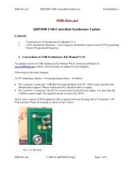
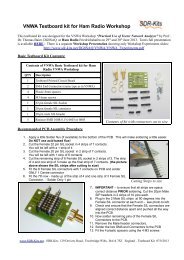
3.3 Contents of the <strong>VNWA</strong> 3 <strong>Expansion</strong> Board kit is shown below. check off against the list.<br />
1 pc assembled <strong>VNWA</strong> 3 <strong>Expansion</strong> Board<br />
1 pc 2mm Allen key to remove <strong>VNWA</strong> 3 covers<br />
3 pcs 2.5mm dia 8mm long spacers<br />
3 pcs 2.5mm steel washers<br />
6 pcs 2.5mm dia 6mm screws<br />
6 pcs fibre washers 2. mm dia<br />
3 pcs 3 pin female SIP connectors<br />
1 pc 2 pin female SIP connector<br />
1 pc 6 pin female SIP connector<br />
15 cm solder<br />
3.2 Tools required<br />
Fig 2. <strong>VNWA</strong> 3 <strong>Expansion</strong> Board kit contents<br />
2mm allen key (supplied with kit)<br />
Small crosshead screwdriver<br />
Sharp Scalpel or hobby knife<br />
Tweezers<br />
25W or 40W soldering - preferably temperature controlled<br />
small inspection mirror<br />
<strong>SDR</strong>-<strong>Kits</strong> <strong>VNWA</strong> 3 <strong>Expansion</strong> Board <strong>v1</strong>.1 - Copyright 2011 by <strong>SDR</strong>-<strong>Kits</strong> Page 3 of 10
4.0 Fitting <strong>VNWA</strong> 3 <strong>Expansion</strong> Board<br />
4.1 <strong>VNWA</strong> <strong>Expansion</strong> Board fittings<br />
4.1.1 Caution - observe Antistatic precautions -<br />
4.1.2 Remove the Top and Bottom enclosure covers of the <strong>VNWA</strong> 3 using the Allen key supplied.<br />
4.1.3 If you are planning to use the RJ11 connector for external <strong>VNWA</strong> connections, cut out the<br />
square hole for the RJ11 in the rear panel label using a sharp hobby knife or scalpel as shown<br />
in fig 4.<br />
4.1.4 If you plan to fit the optional clock input/output cut out the round hole to fit an SMA<br />
connector as shown in fig 3.<br />
Fig 3. Holes cut in Rear label for RJ11 and optional SMA external Clock connector.<br />
Also shown is the Jumper which needs to be removed for <strong>VNWA</strong> 3 with s/n 2201 and higher<br />
note: Chassis Hole Clock connector is only provided in <strong>VNWA</strong>3 with s/n 2201 and higher<br />
4.1.5 Remove <strong>VNWA</strong> <strong>Expansion</strong> Board from packaging and fit the 3 spacers as shown below. the<br />
correct sequence is:<br />
2.5 mm screw<br />
2.5 mm fibre washer on top of the PCB<br />
then 2.5mm steel wash below the PCB<br />
followed by the 8mm long spacer<br />
<strong>SDR</strong>-<strong>Kits</strong> <strong>VNWA</strong> 3 <strong>Expansion</strong> Board <strong>v1</strong>.1 - Copyright 2011 by <strong>SDR</strong>-<strong>Kits</strong> Page 4 of 10
Fig 4. <strong>VNWA</strong> 3 <strong>Expansion</strong> Board - bottom view<br />
4.2 <strong>VNWA</strong> 3 with Serial numbers between A2001 and A2200 requiring Soldering:<br />
4.2.1 Fit the female SIP connectors to the male SIP connectors to the <strong>VNWA</strong> 3 <strong>Expansion</strong> Board.<br />
4.2.3 Next fit the <strong>VNWA</strong> 3 Breakout PCB with the mating SIP connectors to the <strong>VNWA</strong> 3 main pcb.<br />
Make sure that all SIP connector pins are visible as shown below.<br />
4.2.3 Check whether Breakout PCB is correctly positioned and fasten the <strong>VNWA</strong> 3 Breakout PCB<br />
to the main <strong>VNWA</strong> PCB using 3 pcs 2.5 mm screws and fibre washers as shown in Fig 6.<br />
4.2.4 Now solder the connectors J31, J52, J36, J34 and J53 on the <strong>VNWA</strong> Main PCB<br />
4.2.5 Refer to figure 5. Locate Zero Ohm resistor A which is fitted on <strong>VNWA</strong> 3 with s/n 2200 or<br />
less. Resistor A must be removed for operation of the DDS with DC power from the <strong>VNWA</strong> 3<br />
<strong>Expansion</strong> <strong>board</strong>.<br />
4.2.6 Caution do not cut the resistor or use force as the PCB track could be damaged.<br />
4.2.7 The best method is to remove excess solder with solder wick first and heat both ends of the<br />
resistor at the same time. The resistor can now be "swiped sideways" and removed.<br />
Fig 5. <strong>VNWA</strong> 3 - Removing Jumper A<br />
<strong>SDR</strong>-<strong>Kits</strong> <strong>VNWA</strong> 3 <strong>Expansion</strong> Board <strong>v1</strong>.1 - Copyright 2011 by <strong>SDR</strong>-<strong>Kits</strong> Page 5 of 10
4.2.8 Refit <strong>VNWA</strong> top and bottom enclosures. Make sure the EMC shield strips fit properly on the<br />
horizontal chassis to avoid RF leakage. Do Not overtighten the eclosure screws<br />
Fig 6. Top view of <strong>VNWA</strong> 3 Main PCB showing where SIP connectors are soldered<br />
4.3 <strong>VNWA</strong> 3 with Serial numbers A2201 and higher (SIP connectors already fitted)<br />
4.3.1 Remove the 2 pin Jumper as shown in fig 3. The jumper is secured with a blob of hot glue on<br />
the side which should removed with a pen knife first<br />
4.3.2 Plug in the <strong>VNWA</strong> 3 Breakout PCB onto the main <strong>VNWA</strong> PCB.<br />
Use a small inspection mirror to check the connectors are properly aligned before<br />
pressing down. Do not exert undue force, if necessary remove the PCB and start again.<br />
4.3.3 After Breakout PCB has been fitted check with inspection mirror whether all the connectors<br />
are mated.<br />
4.3.4 Fasten the <strong>VNWA</strong> 3 Breakout PCB to the main <strong>VNWA</strong> PCB using the 3 2.5 mm screws and<br />
fibre washers as shown in Fig 6.<br />
4.3.5 Refit <strong>VNWA</strong> top and bottom enclosures. Make sure the EMC shield strips fit properly on the<br />
horizontal chassis to avoid RF leakage. Do Not overtighten the eclosure screws<br />
5. Commissioning & Configuring <strong>VNWA</strong> 3 Audio Codec<br />
5.1.1 Plug the <strong>VNWA</strong> 3 with <strong>Expansion</strong> Board fitted into USB port of Personal Computer.<br />
5.1.2 Monitor briefly for any unusual symptoms and/or messages from Windows Operating<br />
System: If window pops up that the USB-current is exceeded, remove <strong>VNWA</strong> immediately<br />
and check for any short circuits and errors in the <strong>VNWA</strong> 3 Breakout <strong>board</strong> installation<br />
5.1.3 Start the <strong>VNWA</strong> Application, then goto "File" and "Setup" "USB Settings" and perform "Test<br />
<strong>SDR</strong>-<strong>Kits</strong> <strong>VNWA</strong> 3 <strong>Expansion</strong> Board <strong>v1</strong>.1 - Copyright 2011 by <strong>SDR</strong>-<strong>Kits</strong> Page 6 of 10
USB Interface" to confirm that <strong>VNWA</strong> is operational.<br />
5.1.4 Select Tab "Audio Level" and tick the box "Auxilary Audio Capture Device Available" in fig 7.<br />
which is applicable for Windows XP operating system.<br />
This will bring up the configuration of the Auxilary Audio Capture Device. Change the<br />
settings as shown in fig 7. as appropriate.<br />
Troubleshooting: If "Auxiliary Audio Capture Device available" is NOT shown, then exit <strong>VNWA</strong><br />
application and add the line AuxAudio=1 to the file <strong>VNWA</strong>.ini with a text editor and then<br />
restart the <strong>VNWA</strong> Application. See also <strong>VNWA</strong> helpfile<br />
Note: With the <strong>VNWA</strong> 3 Breakout PCB fitted there are now two USB Codec devices, a) USB Audio<br />
Codec and b) USB Audio Codec 2. The built-in USB codec must be the main capture device, as it is<br />
hard wired to the multiplexing switch. USB-Codec configuration is done in the following step:<br />
5.1.5 Press button "Calibrate Sample Rate" as shown in fig 7. If Sample Calibration Rate fails<br />
(First pulse not detected) then reverse the two USB Audio Codec devices and test again.<br />
(ie Audio Capture becomes "USB Audio Codec" and Aux. Audio Capture becomes "USB<br />
Audio Codec 2")<br />
Fig 7. Configuration of Auxiliary Audio Capture Device<br />
5.1.6 Now select the tab "Audio Level" and select "Reflect" mode and with no termination on the TXport,<br />
and check the blue main Reference signal and blue Reflected signal are as shown in fig<br />
8. Do not worry about the lighter red Aux Audio signal, which may also be visible.<br />
<strong>SDR</strong>-<strong>Kits</strong> <strong>VNWA</strong> 3 <strong>Expansion</strong> Board <strong>v1</strong>.1 - Copyright 2011 by <strong>SDR</strong>-<strong>Kits</strong> Page 7 of 10
Note: If the sinewaves are "clipped" (Vista or Windows 7) then the Recording level of the relevant<br />
USB Audio Codec needs to be changed. Also check whether the USB Audio Codec is set to<br />
Stereo 48 Kbps as described in the "Getting Started" booklet shipped with the <strong>VNWA</strong> or see<br />
the <strong>VNWA</strong> Helpfile<br />
Fig 8. Audio Level with TX port not terminated (full Reflection)<br />
5.1.7. Connect a short coax cable between TX and RX ports and check the Reflect sinewave in Fig 8.<br />
now becomes a flat blue line.<br />
5.1.8 Next select the tab "Aux. Audio Level" and check the display as shown in fig 9. is obtained.<br />
Note: If the sinewaves are "clipped" (Vista or Windows 7) then the Recording level of the relevant<br />
USB Audio Codec needs to be changed. Also check whether the USB Audio Codec is set to<br />
Stereo 48 Kbps as described in the "Getting Started" booklet shipped with the <strong>VNWA</strong> or see t<br />
he <strong>VNWA</strong> Helpfile - Section "Configuration - Vista / Windows 7 audio issues"<br />
<strong>SDR</strong>-<strong>Kits</strong> <strong>VNWA</strong> 3 <strong>Expansion</strong> Board <strong>v1</strong>.1 - Copyright 2011 by <strong>SDR</strong>-<strong>Kits</strong> Page 8 of 10
Fig 9. Aux. Audio Level with TX and RX ports connected<br />
Troubleshooting: If the above displays are not obtained then check the USB-Audio Settings in fig 7.<br />
and perform step 5.1.5 again.<br />
6. <strong>VNWA</strong> 3 <strong>Expansion</strong> Board Interface information:<br />
The <strong>VNWA</strong>3 combines the <strong>VNWA</strong> and the USB interface functionality on a single 100x60mm² <strong>board</strong>:<br />
The <strong>VNWA</strong>3 only requires a single USB cable to connect to a PC. The interface options are shown in<br />
7.1 and 7.2 Also refer to the <strong>VNWA</strong> Helpfile for a block diagram and Application configuration options<br />
for the Rotor Start/stop and S-Parameter switch options.<br />
6.1 <strong>VNWA</strong> 3 <strong>Expansion</strong> Board - External Connections<br />
RJ11<br />
pin<br />
Pin 1:<br />
Signal Description<br />
Rotor start/stop control signal<br />
(input)<br />
Cable<br />
colour<br />
white<br />
Pin 2: Not Connected black<br />
Pin 3:<br />
S-Parameter Test set Control<br />
Signal (output)<br />
red<br />
Pin 4: Not Connected green<br />
Remarks:<br />
(see also <strong>VNWA</strong> helpfile for info on options)<br />
Input signal, normally +3.3V. When input is<br />
grounded, <strong>VNWA</strong> sweep and the rotor engine are<br />
started for Radar type Antenna plots<br />
0 or 3.3V Logic DC Signal from AVR via 680 series<br />
resistor. See Helpfile for configuration details<br />
<strong>SDR</strong>-<strong>Kits</strong> <strong>VNWA</strong> 3 <strong>Expansion</strong> Board <strong>v1</strong>.1 - Copyright 2011 by <strong>SDR</strong>-<strong>Kits</strong> Page 9 of 10
Pin 5:<br />
Internal 5V DC Power out or<br />
External 5V Power In<br />
(See Note 1)<br />
yellow<br />
A maximum of about 100mA may be drawn from<br />
internal power provided PC USB Hub can supply<br />
500mA. See Note 1; when using external power<br />
Pin 6 Ground blue <strong>VNWA</strong> Ground Connection<br />
Note 1: For operating the <strong>VNWA</strong>3 from an external 5V DC power supply, zero Ohm<br />
resistor B shown in Fig 5. must be removed from the <strong>VNWA</strong>3 <strong>board</strong><br />
Note 2: Cable colour refers to the colours of the optional RJ11 cable available from <strong>SDR</strong>-<strong>Kits</strong><br />
6.2 Optional External Clock input/output<br />
An Optional SMA connector may be fitted for connecting an External 36 MHz Clock output or to tap<br />
the internal multiplied System clock. After the <strong>VNWA</strong> 3 <strong>Expansion</strong> Board is fitted, the SMA connector<br />
is fitted in the 8mm round hole provided only in <strong>VNWA</strong>3 with s/n 2201 and higher as shown in fig 1.<br />
With a scalpel cut a round hole in the rear panel label and fit the SMA connector.<br />
solder a short wire between the SMA center connector to the PCB track. Soldering of ground<br />
connections is not required.<br />
If the SMA connector is not used then it is recommended to fit an SMA Screening cap to prevent<br />
radiation from and damage to the SMA connector.<br />
6.3 Specification of the <strong>VNWA</strong> Reference Clock output or External Clock input:<br />
Internal Clock Output: TCXO 12 MHz*x (x=2..8) 2ppm Out - 1kOhm impedance, 400mVpp<br />
output<br />
External Reference Clock: ideally 36 MHz with level of between -6dBm...+3dBm / 50 Ohms<br />
7.0 WEEE, Disposal of Waste Electrical Equipment<br />
This symbol on the product indicates that this product should not be treated as<br />
household waste.<br />
Instead it should be handed over to a suitable collection point for the recycling of<br />
electrical and electronic equipment. Users of this product in the European Community<br />
should contact <strong>SDR</strong>-<strong>Kits</strong> to specific arrangements for the disposal and recycling of this<br />
product in accordance with the relevant EEC Directives.<br />
7.1 CE Certification,<br />
This product is CE certified according to the provisions of 2004/108/EC and 1995/5/EC<br />
relating to the Radio and Telecommunications Terminal Equipment (R&TTE) is in compliance<br />
with the essential requirements of these directives.<br />
8. Contact adress<br />
<strong>SDR</strong>-<strong>Kits</strong> (Internet & mail order only)<br />
14 Ragleth Grove<br />
Trowbridge, Wilts BA14-7LE<br />
United Kingdom<br />
email: sdrkits@gmail.com<br />
www.<strong>SDR</strong>-<strong>Kits</strong>.net<br />
<strong>SDR</strong>-<strong>Kits</strong> <strong>VNWA</strong> 3 <strong>Expansion</strong> Board <strong>v1</strong>.1 - Copyright 2011 by <strong>SDR</strong>-<strong>Kits</strong> Page 10 of 10