184-Pin Unbuffered Double Data Rate SDRAM UDIMM DDR SDRAM
184-Pin Unbuffered Double Data Rate SDRAM UDIMM DDR SDRAM
184-Pin Unbuffered Double Data Rate SDRAM UDIMM DDR SDRAM

You also want an ePaper? Increase the reach of your titles
YUMPU automatically turns print PDFs into web optimized ePapers that Google loves.
HYS64D32301HU–[5/6]–C<br />
HYS[72/64]D64300HU–[5/6]–C<br />
HYS[64/72]D128320HU–[5/6]–C<br />
<strong>184</strong>-<strong>Pin</strong> <strong>Unbuffered</strong> <strong>Double</strong> <strong>Data</strong> <strong>Rate</strong> <strong>SDRAM</strong><br />
<strong>UDIMM</strong><br />
<strong>DDR</strong> <strong>SDRAM</strong><br />
RoHS Compliant Products<br />
Internet <strong>Data</strong> Sheet<br />
Rev. 1.21<br />
September 2006
HYS64D32301HU–[5/6]–C, HYS[72/64]D64300HU–[5/6]–C, HYS[64/72]D128320HU–[5/6]–C<br />
Revision History: 2006-09, Rev. 1.21<br />
Page Subjects (major changes since last revision)<br />
All Adapted internet edition<br />
Previous Revision: Rev. 1.20, 2005-12<br />
14 changed component configuration for 256MB to 32M x16<br />
26 changed <strong>DDR</strong>400 t RFC from 70 ns to 65 ns<br />
Previous Revision: Rev. 1.10, 2005-05<br />
We Listen to Your Comments<br />
Any information within this document that you feel is wrong, unclear or missing at all?<br />
Your feedback will help us to continuously improve the quality of this document.<br />
Please send your proposal (including a reference to this document) to:<br />
techdoc@qimonda.com<br />
qag_techdoc_rev400 / 3.2 QAG / 2006-08-01 2<br />
03292006-RA8T-MSZL<br />
Internet <strong>Data</strong> Sheet<br />
HYS[64/72]D[16/32/128]3xxHU–[5/6]–C<br />
<strong>Unbuffered</strong> <strong>DDR</strong> <strong>SDRAM</strong> Modules
1 Overview<br />
Rev. 1.21, 2006-09 3<br />
03292006-RA8T-MSZL<br />
Internet <strong>Data</strong> Sheet<br />
HYS[64/72]D[16/32/128]3xxHU–[5/6]–C<br />
<strong>Unbuffered</strong> <strong>DDR</strong> <strong>SDRAM</strong> Modules<br />
This chapter gives an overview of the <strong>184</strong>-<strong>Pin</strong> <strong>Unbuffered</strong> <strong>Double</strong> <strong>Data</strong> <strong>Rate</strong> <strong>SDRAM</strong> product family and describes its main<br />
characteristics.<br />
1.1 Features<br />
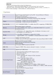
• <strong>184</strong>-<strong>Pin</strong> <strong>Unbuffered</strong> <strong>Double</strong> <strong>Data</strong> <strong>Rate</strong> <strong>SDRAM</strong> (ECC and non-parity) for PC and Workstation main memory applications<br />
• One rank 32M �64, 64M��64, 64M �72 ,and two ranks 128M �64 ,128M �72 organization<br />
• Standard <strong>Double</strong> <strong>Data</strong> <strong>Rate</strong> Synchronous DRAMs (<strong>DDR</strong> <strong>SDRAM</strong>) Single +2.5V (�0.2V) and +2.6V (�0.1V) power supply<br />
for <strong>DDR</strong>400<br />
• Built with 512 Mbit <strong>DDR</strong> <strong>SDRAM</strong> in P-TSOPII-66-1 package<br />
• Programmable CAS Latency, Burst Length, and Wrap Sequence (Sequential & Interleave)<br />
• Auto Refresh (CBR) and Self Refresh<br />
• RAS-lockout supported t RAP=t RCD<br />
• All inputs and outputs SSTL_2 compatible<br />
• Serial Presence Detect with E 2 PROM<br />
• Standard MO-206 form factor: 133.35 mm � 31.75 mm � 4.00 mm max.<br />
• Standard reference layout for raw cards: A, B and C<br />
• Gold plated contacts<br />
• RoHS Compliant Product 1)<br />
TABLE 1<br />
Performance<br />
Part Number Speed Code –5 –6 Unit<br />
Speed Grade Component <strong>DDR</strong>400B <strong>DDR</strong>333B —<br />
Module PC3200–3033 PC2700–2533 —<br />
max. Clock Frequency @CL3 fCK3 200 166 MHz<br />
@CL2.5 fCK2.5 166 166 MHz<br />
@CL2 fCK2 133 133 MHz<br />
1) RoHS Compliant Product: Restriction of the use of certain hazardous substances (RoHS) in electrical and electronic equipment as defined<br />
in the directive 2002/95/EC issued by the European Parliament and of the Council of 27 January 2003. These substances include mercury,<br />
lead, cadmium, hexavalent chromium, polybrominated biphenyls and polybrominated biphenyl ethers.
1.2 Description<br />
The HYS64D32301HU–[5/6]–C, HYS[72/64]D64300HU–<br />
[5/6]–C, HYS[64/72]D128320HU–[5/6]–C, and are industry<br />
standard <strong>184</strong>-<strong>Pin</strong> <strong>Unbuffered</strong> <strong>Double</strong><br />
<strong>Data</strong> <strong>Rate</strong> <strong>SDRAM</strong> (<strong>UDIMM</strong>) organized as<br />
32M � 64 (256 MB), 64M � 64 (512 MB), 128M � 64 (1 GB)<br />
for non-parity and 64M � 72 (512 MB), 128M � 72 (1 GB) for<br />
ECC main memory applications. The memory array is<br />
Product Type 1)<br />
Rev. 1.21, 2006-09 4<br />
03292006-RA8T-MSZL<br />
Internet <strong>Data</strong> Sheet<br />
HYS[64/72]D[16/32/128]3xxHU–[5/6]–C<br />
<strong>Unbuffered</strong> <strong>DDR</strong> <strong>SDRAM</strong> Modules<br />
designed with 512Mbit <strong>Double</strong> <strong>Data</strong> <strong>Rate</strong> Synchronous<br />
DRAMs. A variety of decoupling capacitors are mounted on<br />
the printed circuit board. The DIMMs feature serial presence<br />
detect (SPD) based on a serial E 2 PROM device using the 2pin<br />
I2C protocol. The first 128 bytes are programmed with<br />
configuration data and the second 128 bytes are available to<br />
the customer<br />
TABLE 2<br />
Ordering Information for Lead-Free Products (RoHSCompliant Product)<br />
Compliance Code 2)<br />
Description <strong>SDRAM</strong> Technology<br />
PC3200 (CL=3.0)<br />
HYS64D32301HU–5–C PC3200U–30331–C3 one rank 256 MB DIMM 512 Mbit (�16)<br />
HYS64D64300HU–5–C PC3200U–30331–A1 one rank 512 MB DIMM 512 Mbit (�8)<br />
HYS72D64300HU–5–C PC3200U–30331–A1 one rank 512 MB ECC-DIMM 512 Mbit (�8)<br />
HYS64D128320HU–5–C PC3200U–30331–B2 two ranks 1 GB DIMM 512 Mbit (�8)<br />
HYS72D128320HU–5–C<br />
PC2700 (CL=2.5)<br />
PC3200U–30331–B2 two ranks 1 GB ECC-DIMM 512 Mbit (�8)<br />
HYS64D32301HU–6–C PC2700U–25331–C3 one rank 256 MB DIMM 512 Mbit (�16)<br />
HYS64D64300HU–6–C PC2700U–25331–A1 one rank 512 MB DIMM 512 Mbit (�8)<br />
HYS72D64300HU–6–C PC2700U–25331–A1 one rank 512 MB ECC-DIMM 512 Mbit (�8)<br />
HYS64D128320HU–6–C PC2700U–25331–B2 two ranks 1 GB DIMM 512 Mbit (�8)<br />
HYS72D128320HU–6–C PC2700U–25331–B2 two ranks 1 GB ECC-DIMM 512 Mbit (�8)<br />
1) All product types end with a place code designating the silicon-die revision. Reference information available on request. Example:<br />
HYS64D128320HU–5–C, indicating Rev.C die are used for <strong>SDRAM</strong> components.<br />
2) The Compliance Code is printed on the module labels and describes the speed sort (for example “PC3200”), the latencies (for example<br />
“30330” means CAS latency of 3.0 clocks, Row-Column-Delay (RCD) latency of 3 clocks and Row Precharge latency of 3 clocks), JEDEC<br />
SPD code definition version 0, and the Raw Card used for this module.
2 <strong>Pin</strong> Configuration<br />
The pin configuration of the <strong>Unbuffered</strong> <strong>DDR</strong> <strong>SDRAM</strong> DIMM<br />
is listed by function in Table 3 (<strong>184</strong> pins). The abbreviations<br />
used in columns <strong>Pin</strong> and Buffer Type are explained in Table 4<br />
<strong>Pin</strong># Name <strong>Pin</strong><br />
Type<br />
Buffer<br />
Type<br />
Rev. 1.21, 2006-09 5<br />
03292006-RA8T-MSZL<br />
Internet <strong>Data</strong> Sheet<br />
HYS[64/72]D[16/32/128]3xxHU–[5/6]–C<br />
<strong>Unbuffered</strong> <strong>DDR</strong> <strong>SDRAM</strong> Modules<br />
and Table 5 respectively. The pin numbering is depicted in<br />
Figure 1.<br />
Function<br />
Clock Signals<br />
137 CK0 I SSTL Clock Signals 2:0<br />
NC NC –<br />
16 CK1 I SSTL<br />
76 CK2 I SSTL<br />
138 CK0 I SSTL Complement Clock Signals 2:0<br />
NC NC –<br />
17 CK1 I SSTL<br />
75 CK2 I SSTL<br />
21 CKE0 I SSTL Clock Enable Rank 0<br />
111 CKE1 I SSTL Clock Enable Rank 1<br />
Note: 2-rank module<br />
NC NC – Note: 1-rank module<br />
Control Signals<br />
157 S0 I SSTL Chip Select Rank 0<br />
158 S1 I SSTL Chip Select Rank 1<br />
Note: 2-rank module<br />
NC NC – Note: 1-rank module<br />
154 RAS I SSTL Row Address Strobe<br />
65 CAS I SSTL Column Address Strobe<br />
63 WE I SSTL Write Enable<br />
Address Signals<br />
59 BA0 I SSTL Bank Address Bus 2:0<br />
52 BA1 I SSTL<br />
TABLE 3<br />
<strong>Pin</strong> Configuration of <strong>UDIMM</strong>
<strong>Pin</strong># Name <strong>Pin</strong><br />
Type<br />
Buffer<br />
Type<br />
Rev. 1.21, 2006-09 6<br />
03292006-RA8T-MSZL<br />
Function<br />
Internet <strong>Data</strong> Sheet<br />
HYS[64/72]D[16/32/128]3xxHU–[5/6]–C<br />
<strong>Unbuffered</strong> <strong>DDR</strong> <strong>SDRAM</strong> Modules<br />
48 A0 I SSTL Address Bus 11:0<br />
43 A1 I SSTL<br />
41 A2 I SSTL<br />
130 A3 I SSTL<br />
37 A4 I SSTL<br />
32 A5 I SSTL<br />
125 A6 I SSTL<br />
29 A7 I SSTL<br />
122 A8 I SSTL Address Bus 11:0<br />
27 A9 I SSTL<br />
141 A10 I SSTL<br />
AP I SSTL<br />
118 A11 I SSTL<br />
115 A12 I SSTL Address Signal 12<br />
Note: Module based on 256 Mbit or larger dies<br />
NC NC – Note: 128 Mbit based module<br />
167 A13 I SSTL Address Signal 13<br />
Note: 1 Gbit based module<br />
NC NC – Note: Module based on 512 Mbit or smaller dies
<strong>Pin</strong># Name <strong>Pin</strong><br />
Type<br />
Buffer<br />
Type<br />
<strong>Data</strong> Signals<br />
2 DQ0 I/O SSTL <strong>Data</strong> Bus 63:0<br />
4 DQ1 I/O SSTL<br />
6 DQ2 I/O SSTL<br />
8 DQ3 I/O SSTL<br />
94 DQ4 I/O SSTL<br />
95 DQ5 I/O SSTL<br />
98 DQ6 I/O SSTL<br />
99 DQ7 I/O SSTL<br />
12 DQ8 I/O SSTL<br />
13 DQ9 I/O SSTL<br />
19 DQ10 I/O SSTL<br />
20 DQ11 I/O SSTL<br />
105 DQ12 I/O SSTL<br />
106 DQ13 I/O SSTL<br />
109 DQ14 I/O SSTL<br />
110 DQ15 I/O SSTL<br />
23 DQ16 I/O SSTL<br />
24 DQ17 I/O SSTL<br />
28 DQ18 I/O SSTL<br />
31 DQ19 I/O SSTL<br />
114 DQ20 I/O SSTL<br />
117 DQ21 I/O SSTL<br />
Rev. 1.21, 2006-09 7<br />
03292006-RA8T-MSZL<br />
Function<br />
Internet <strong>Data</strong> Sheet<br />
HYS[64/72]D[16/32/128]3xxHU–[5/6]–C<br />
<strong>Unbuffered</strong> <strong>DDR</strong> <strong>SDRAM</strong> Modules
<strong>Pin</strong># Name <strong>Pin</strong><br />
Type<br />
Buffer<br />
Type<br />
121 DQ22 I/O SSTL <strong>Data</strong> Bus 63:0<br />
123 DQ23 I/O SSTL<br />
33 DQ24 I/O SSTL<br />
35 DQ25 I/O SSTL<br />
39 DQ26 I/O SSTL<br />
40 DQ27 I/O SSTL<br />
126 DQ28 I/O SSTL<br />
127 DQ29 I/O SSTL<br />
131 DQ30 I/O SSTL<br />
133 DQ31 I/O SSTL<br />
53 DQ32 I/O SSTL<br />
55 DQ33 I/O SSTL<br />
57 DQ34 I/O SSTL<br />
60 DQ35 I/O SSTL<br />
146 DQ36 I/O SSTL<br />
147 DQ37 I/O SSTL<br />
150 DQ38 I/O SSTL<br />
151 DQ39 I/O SSTL<br />
61 DQ40 I/O SSTL<br />
64 DQ41 I/O SSTL<br />
68 DQ42 I/O SSTL<br />
69 DQ43 I/O SSTL<br />
153 DQ44 I/O SSTL<br />
155 DQ45 I/O SSTL<br />
161 DQ46 I/O SSTL<br />
162 DQ47 I/O SSTL<br />
72 DQ48 I/O SSTL<br />
73 DQ49 I/O SSTL<br />
79 DQ50 I/O SSTL<br />
80 DQ51 I/O SSTL<br />
165 DQ52 I/O SSTL<br />
166 DQ53 I/O SSTL<br />
170 DQ54 I/O SSTL<br />
171 DQ55 I/O SSTL<br />
83 DQ56 I/O SSTL<br />
84 DQ57 I/O SSTL<br />
87 DQ58 I/O SSTL<br />
88 DQ59 I/O SSTL<br />
174 DQ60 I/O SSTL<br />
175 DQ61 I/O SSTL<br />
Rev. 1.21, 2006-09 8<br />
03292006-RA8T-MSZL<br />
Function<br />
Internet <strong>Data</strong> Sheet<br />
HYS[64/72]D[16/32/128]3xxHU–[5/6]–C<br />
<strong>Unbuffered</strong> <strong>DDR</strong> <strong>SDRAM</strong> Modules
<strong>Pin</strong># Name <strong>Pin</strong><br />
Type<br />
Buffer<br />
Type<br />
178 DQ62 I/O SSTL <strong>Data</strong> Bus 63:0<br />
179 DQ63 I/O SSTL<br />
44 CB0 I/O SSTL Check Bit 0<br />
NC NC –<br />
45 CB1 I/O SSTL Check Bit 1<br />
NC NC –<br />
49 CB2 I/O SSTL Check Bit 2<br />
NC NC –<br />
51 CB3 I/O SSTL Check Bit 3<br />
NC NC –<br />
134 CB4 I/O SSTL Check Bit 4<br />
NC NC –<br />
135 CB5 I/O SSTL Check Bit 5<br />
NC NC –<br />
142 CB6 I/O SSTL Check Bit 6<br />
NC NC –<br />
144 CB7 I/O SSTL Check Bit 7<br />
NC NC –<br />
5 DQS0 I/O SSTL <strong>Data</strong> Strobe Bus 7:0<br />
14 DQS1 I/O SSTL<br />
25 DQS2 I/O SSTL<br />
36 DQS3 I/O SSTL<br />
56 DQS4 I/O SSTL<br />
67 DQS5 I/O SSTL<br />
78 DQS6 I/O SSTL<br />
86 DQS7 I/O SSTL<br />
47 DQS8 I/O SSTL <strong>Data</strong> Strobe 8<br />
NC NC –<br />
97 DM0 I SSTL <strong>Data</strong> Mask Bus 7:0<br />
107 DM1 I SSTL<br />
119 DM2 I SSTL<br />
129 DM3 I SSTL<br />
149 DM4 I SSTL<br />
159 DM5 I SSTL<br />
169 DM6 I SSTL<br />
177 DM7 I SSTL<br />
140 DM8 I SSTL <strong>Data</strong> Mask 8<br />
EEPROM<br />
NC NC –<br />
92 SCL I CMOS Serial Bus Clock<br />
Rev. 1.21, 2006-09 9<br />
03292006-RA8T-MSZL<br />
Function<br />
Internet <strong>Data</strong> Sheet<br />
HYS[64/72]D[16/32/128]3xxHU–[5/6]–C<br />
<strong>Unbuffered</strong> <strong>DDR</strong> <strong>SDRAM</strong> Modules
<strong>Pin</strong># Name <strong>Pin</strong><br />
Type<br />
91 SDA I/O OD Serial Bus <strong>Data</strong><br />
181 SA0 I CMOS Slave Address Select Bus 2:0<br />
182 SA1 I CMOS<br />
183 SA2 I CMOS<br />
Power Supplies<br />
1 VREF AI – I/O Reference Voltage<br />
<strong>184</strong> VDDSPD PWR – EEPROM Power Supply<br />
15,<br />
22,<br />
30,<br />
54,<br />
62,<br />
77,<br />
96,<br />
104,<br />
112,<br />
128,<br />
136,<br />
143,<br />
156,<br />
164,<br />
172,<br />
180<br />
VDDQ PWR – I/O Driver Power Supply<br />
7,<br />
38,<br />
46,<br />
70,<br />
85,<br />
108,<br />
120,<br />
148,<br />
168<br />
Buffer<br />
Type<br />
V DD PWR – Power Supply<br />
Rev. 1.21, 2006-09 10<br />
03292006-RA8T-MSZL<br />
Function<br />
Internet <strong>Data</strong> Sheet<br />
HYS[64/72]D[16/32/128]3xxHU–[5/6]–C<br />
<strong>Unbuffered</strong> <strong>DDR</strong> <strong>SDRAM</strong> Modules
<strong>Pin</strong># Name <strong>Pin</strong><br />
Type<br />
3,<br />
11,<br />
18,<br />
26,<br />
34,<br />
42,<br />
50,<br />
58,<br />
66,<br />
74,<br />
81,<br />
89,<br />
93,<br />
100,<br />
116,<br />
124,<br />
132,<br />
139,<br />
145,<br />
152,<br />
160,<br />
176<br />
Buffer<br />
Type<br />
V SS GND – Ground Plane<br />
Other <strong>Pin</strong>s<br />
82 VDDID O OD VDD Identification<br />
9,<br />
10,<br />
71,<br />
90,<br />
101,<br />
102,<br />
103,<br />
113,<br />
163,<br />
173<br />
NC NC – Not connected<br />
Rev. 1.21, 2006-09 11<br />
03292006-RA8T-MSZL<br />
Function<br />
Internet <strong>Data</strong> Sheet<br />
HYS[64/72]D[16/32/128]3xxHU–[5/6]–C<br />
<strong>Unbuffered</strong> <strong>DDR</strong> <strong>SDRAM</strong> Modules
Abbreviation Description<br />
I Standard input-only pin. Digital levels.<br />
O Output. Digital levels.<br />
I/O I/O is a bidirectional input/output signal.<br />
AI Input. Analog levels.<br />
PWR Power<br />
GND Ground<br />
NC Not Connected<br />
Abbreviation Description<br />
Rev. 1.21, 2006-09 12<br />
03292006-RA8T-MSZL<br />
Internet <strong>Data</strong> Sheet<br />
HYS[64/72]D[16/32/128]3xxHU–[5/6]–C<br />
<strong>Unbuffered</strong> <strong>DDR</strong> <strong>SDRAM</strong> Modules<br />
TABLE 4<br />
Abbreviations for <strong>Pin</strong> Type<br />
TABLE 5<br />
Abbreviations for Buffer Type<br />
SSTL Serial Stub Terminated Logic (SSTL2)<br />
LV-CMOS Low Voltage CMOS<br />
CMOS CMOS Levels<br />
OD Open Drain. The corresponding pin has 2 operational states, active low and tristate,<br />
and allows multiple devices to share as a wire-OR.
�� ������<br />
�� ��������������<br />
�� �� ��������������<br />
����<br />
����������<br />
��������������<br />
�� �� ��������������<br />
����<br />
������<br />
��������������<br />
�������� ��������������<br />
����������<br />
��������������<br />
���������� ��������������<br />
��������<br />
��������������<br />
����������<br />
��������������<br />
�������� �� ��������������<br />
�������� �� ��������������<br />
�������� �� ��������������<br />
���� �� ��������������<br />
���� �� ��������������<br />
�������� �� ��������������<br />
�������� �� ��������������<br />
�������� �� ��������������<br />
������ �� ��������������<br />
�������� �� ��������������<br />
���� �� ��������������<br />
���� �� ��������������<br />
�������������� �� ��������������<br />
�������������� �� ��������������<br />
�������������� �� ��������������<br />
�������������� �� ��������������<br />
����������<br />
��������������<br />
����������<br />
��������������<br />
����������<br />
��������������<br />
������ �� ��������������<br />
����������<br />
��������������<br />
������<br />
��������������<br />
������ �� ��������������<br />
����������<br />
��������������<br />
����������<br />
��������������<br />
������<br />
��������������<br />
����������<br />
��������������<br />
��������<br />
��������������<br />
�� �� ������ ��������������<br />
����������<br />
��������������<br />
�� �� ���� ��������������<br />
����������<br />
��������������<br />
������ �� ��������������<br />
����������<br />
��������������<br />
������ �� ��������������<br />
������ �� ��������������<br />
����������<br />
��������������<br />
����������<br />
��������������<br />
����������<br />
��������������<br />
����������<br />
��������������<br />
������<br />
��������������<br />
����������<br />
��������������<br />
����������<br />
��������������<br />
��������<br />
��������������<br />
�������� ��������������<br />
����������<br />
��������������<br />
�������� �� ��������������<br />
�������� �� ��������������<br />
������ �� ��������������<br />
�������� �� ��������������<br />
�������� �� ��������������<br />
���� �� ��������������<br />
������ �� ��������������<br />
�������� �� ��������������<br />
������ �� ��������������<br />
�������� �� ��������������<br />
������ �� ��������������<br />
�������������� �� ��������������<br />
������ �� ��������������<br />
���� �� ��������������<br />
������ �� ��������������<br />
������ �� ��������������<br />
�� ������<br />
�� ��������������<br />
�������� �� ��������������<br />
������ �� ��������������<br />
�������� �� ��������������<br />
�������� �� ��������������<br />
�������� �� ��������������<br />
������ �� ��������������<br />
�������� �� ��������������<br />
������ �� ��������������<br />
�������� �� ��������������<br />
������ �� ��������������<br />
������ �� ��������������<br />
�������� �� ��������������<br />
�������� �� ��������������<br />
���������� �� ��������������<br />
�������� �� ��������������<br />
�������� �� ��������������<br />
�������� �� ��������������<br />
���� �� ��������������<br />
������ �� ��������������<br />
Notes<br />
1. VDD = VDDQ , therefore VDDID strap open<br />
Rev. 1.21, 2006-09 13<br />
03292006-RA8T-MSZL<br />
��<br />
��<br />
��<br />
��<br />
��<br />
��<br />
��<br />
��<br />
��<br />
��<br />
��<br />
��<br />
��<br />
��<br />
��<br />
��<br />
��<br />
Internet <strong>Data</strong> Sheet<br />
HYS[64/72]D[16/32/128]3xxHU–[5/6]–C<br />
<strong>Unbuffered</strong> <strong>DDR</strong> <strong>SDRAM</strong> Modules<br />
FIGURE 1<br />
<strong>Pin</strong> Configuration <strong>184</strong>-<strong>Pin</strong>, <strong>UDIMM</strong><br />
�������������� ����������<br />
�������������� ����������<br />
�������������� ����������<br />
�������������� ��������<br />
�������������� ������<br />
�������������� ����������<br />
�������������� ����������<br />
�������������� ��������<br />
�������������� ����������<br />
�������������� ����������<br />
�������������� ����������<br />
�������������� ��������<br />
�������������� ��������<br />
�������������� ��������<br />
�������������� ������<br />
�������������� ��������<br />
�������������� ����������<br />
�������������� ����������<br />
�������������� ������<br />
�������������� ��������<br />
�������������� ��������������<br />
�������������� ����������<br />
�������������� ��������������<br />
�������������� ��������������<br />
�������������� ����������������<br />
�������������� ��������������<br />
����������������<br />
��������<br />
����������������<br />
������ ����������������<br />
��������<br />
����������������<br />
������ ����������������<br />
������<br />
����������������<br />
�������� ����������������<br />
����������<br />
����������������<br />
������ ����������������<br />
��������<br />
����������������<br />
�������� ����������������<br />
��������<br />
����������������<br />
������ ����������������<br />
��������<br />
����������������<br />
�������� ����������������<br />
��������<br />
����������������<br />
������ ����������������<br />
��������<br />
����������������<br />
�������� ����������������<br />
������<br />
����������������<br />
�� ����������<br />
����������������<br />
������ ����������������<br />
��������<br />
����������������<br />
������<br />
����������������<br />
��������<br />
����������������<br />
����<br />
����������������<br />
����<br />
����������������<br />
��������<br />
����������������<br />
������<br />
����������������<br />
��������<br />
����������������<br />
��������������<br />
����������������<br />
����<br />
����������������<br />
������������<br />
����������������<br />
��������<br />
����������������<br />
������<br />
����������������<br />
��������<br />
����������������<br />
��������<br />
����������������<br />
����<br />
����������������<br />
��������<br />
����������������<br />
������<br />
����������������<br />
��������<br />
����������������<br />
��������<br />
����������������<br />
������������<br />
����������������<br />
������������<br />
����������������<br />
������ ����������������<br />
������������<br />
����������������<br />
�� ������<br />
����������������<br />
������ ����������������<br />
��������<br />
����������������<br />
������<br />
����������������<br />
��������<br />
����������������<br />
��������<br />
����������������<br />
��������<br />
����������������<br />
����<br />
����������������<br />
������<br />
����������������<br />
��������<br />
����������������<br />
����<br />
����������������<br />
��������<br />
����������������<br />
������������<br />
����������������<br />
������<br />
����������������<br />
��������<br />
����������������<br />
����<br />
����������������<br />
��������<br />
����������������<br />
������<br />
����������������<br />
��������<br />
����������������<br />
������<br />
����������������<br />
������<br />
����������������<br />
2. DQ, DQS, DM resistors are 22 ��5%<br />
3. BAn, An, RAS, CAS, WE resistors are 3 ��5%
Density Organization Memory<br />
Ranks<br />
<strong>SDRAM</strong>s # of<br />
<strong>SDRAM</strong>s<br />
Rev. 1.21, 2006-09 14<br />
03292006-RA8T-MSZL<br />
# of row/bank/<br />
columns bits<br />
Internet <strong>Data</strong> Sheet<br />
HYS[64/72]D[16/32/128]3xxHU–[5/6]–C<br />
<strong>Unbuffered</strong> <strong>DDR</strong> <strong>SDRAM</strong> Modules<br />
TABLE 6<br />
Address Format<br />
Refresh Period Interval<br />
256 MB 32M �64 1 32M �16 4 13/2/10 8K 64 ms 7.8 ms<br />
512 MB 64M �64 1 64M �8 8 13/2/11 8K 64 ms 7.8 ms<br />
512 MB 64M �72 1 64M �8 9 13/2/11 8K 64 ms 7.8 ms<br />
1GB 128M�64 2 64M �8 16 13/2/11 8K 64 ms 7.8 ms<br />
1GB 128M�72 2 64M �8 18 13/2/11 8K 64 ms 7.8 ms
3 Electrical Characteristics<br />
3.1 Operating Conditions<br />
Rev. 1.21, 2006-09 21<br />
03292006-RA8T-MSZL<br />
Internet <strong>Data</strong> Sheet<br />
HYS[64/72]D[16/32/128]3xxHU–[5/6]–C<br />
<strong>Unbuffered</strong> <strong>DDR</strong> <strong>SDRAM</strong> Modules<br />
TABLE 12<br />
Absolute Maximum Ratings<br />
Parameter Symbol Values Unit Note/ Test<br />
Condition<br />
min. typ. max.<br />
Voltage on I/O pins relative to VSS VIN , VOUT –0.5 – VDDQ + 0.5 V –<br />
Voltage on inputs relative to VSS VIN –1 – +3.6 V –<br />
Voltage on VDD supply relative to VSS VDD –1 – +3.6 V –<br />
Voltage on VDDQ supply relative to VSS VDDQ –1 – +3.6 V –<br />
Operating temperature (ambient) TA 0 – +70 �C –<br />
Storage temperature (plastic) TSTG -55 – +150 �C –<br />
Power dissipation (per <strong>SDRAM</strong> component) PD – 1 – W –<br />
Short circuit output current I OUT – 50 – mA –<br />
Attention: Permanent damage to the device may occur if “Absolute Maximum Ratings” are exceeded. This is a stress<br />
rating only, and functional operation should be restricted to recommended operation conditions. Exposure<br />
to absolute maximum rating conditions for extended periods of time may affect device reliability and<br />
exceeding only one of the values may cause irreversible damage to the integrated circuit.<br />
TABLE 13<br />
Electrical Characteristics and DC Operating Conditions<br />
Parameter Symbol Values Unit Note/Test Condition 1)<br />
Min. Typ. Max.<br />
Device Supply Voltage VDD 2.3 2.5 2.7 V fck � 166 MHz<br />
Device Supply Voltage VDD 2.5 2.6 2.7 V fck � 166 MHz 2)<br />
Output Supply Voltage VDDQ 2.3 2.5 2.7 V fck � 166 MHz 3)<br />
Output Supply Voltage VDDQ 2.5 2.6 2.7 V fck � 166 MHz 2)3)<br />
EEPROM supply voltage VDDSPD 2.3 2.5 3.6 V —<br />
Supply Voltage, I/O Supply VSS, 0 0 V —<br />
Voltage<br />
VSSQ Input Reference Voltage VREF 0.49 � VDDQ 0.5 � VDDQ 0.51 � VDDQ V<br />
4)<br />
I/O Termination Voltage<br />
(System)<br />
V TT V REF – 0.04 V REF + 0.04 V<br />
5)
Input High (Logic1) Voltage VIH(DC) VREF + 0.15 VDDQ + 0.3 V 6)<br />
Input Low (Logic0) Voltage VIL(DC) –��� VREF – 0.15 V 6)<br />
Input Voltage Level,<br />
CK and CK Inputs<br />
Input Differential Voltage,<br />
CK and CK Inputs<br />
VI-Matching Pull-up Current<br />
to Pull-down Current<br />
V IN(DC) –��� V DDQ + 0.3 V 6)<br />
V ID(DC) 0.36 V DDQ + 0.6 V<br />
VI Ratio 0.71 1.4 — 8)<br />
Rev. 1.21, 2006-09 22<br />
03292006-RA8T-MSZL<br />
Internet <strong>Data</strong> Sheet<br />
HYS[64/72]D[16/32/128]3xxHU–[5/6]–C<br />
<strong>Unbuffered</strong> <strong>DDR</strong> <strong>SDRAM</strong> Modules<br />
Parameter Symbol Values Unit Note/Test Condition 1)<br />
Input Leakage Current II –2 2 �A Any input 0 V � VIN � VDD; All other pins not under test<br />
=0V 9)<br />
Output Leakage Current IOZ –5 5 �A DQs are disabled;<br />
9)<br />
0V � VOUT � VDDQ Output High Current, Normal<br />
Strength Driver<br />
Output Low Current, Normal<br />
Strength Driver<br />
Min. Typ. Max.<br />
I OH — –16.2 mA V OUT = 1.95 V<br />
I OL 16.2 — mA V OUT = 0.35 V<br />
1) 0 �C � T A � 70 �C; V DDQ = 2.5 V � 0.2 V, V DD = +2.5 V � 0.2 V; VDDQ = 2.6 V ± 0.1 V, VDD = +2.6 V ± 0.1 V (<strong>DDR</strong>400);<br />
2) <strong>DDR</strong>400 conditions apply for all clock frequencies above 166 MHz<br />
3) Under all conditions, V DDQ must be less than or equal to V DD.<br />
4) Peak to peak AC noise on V REF may not exceed ± 2% VREF (DC). VREF is also expected to track noise variations in V DDQ.<br />
5) V TT is not applied directly to the device. V TT is a system supply for signal termination resistors, is expected to be set equal to V REF , and<br />
must track variations in the DC level of V REF.<br />
6) Inputs are not recognized as valid until V REF stabilizes.<br />
7) V ID is the magnitude of the difference between the input level on CK and the input level on CK.<br />
8) The ratio of the pull-up current to the pull-down current is specified for the same temperature and voltage, over the entire temperature and<br />
voltage range, for device drain to source voltage from 0.25 to 1.0 V. For a given output, it represents the maximum difference between<br />
pull-up and pull-down drivers due to process variation.<br />
9) Values are shown per pin.<br />
6)7)
3.2 I DD Specification and Conditions<br />
Rev. 1.21, 2006-09 23<br />
03292006-RA8T-MSZL<br />
Internet <strong>Data</strong> Sheet<br />
HYS[64/72]D[16/32/128]3xxHU–[5/6]–C<br />
<strong>Unbuffered</strong> <strong>DDR</strong> <strong>SDRAM</strong> Modules<br />
TABLE 14<br />
I DD Conditions<br />
Parameter Symbol<br />
Operating Current 0<br />
one bank; active/ precharge; DQ, DM, and DQS inputs changing once per clock cycle;<br />
address and control inputs changing once every two clock cycles.<br />
Operating Current 1<br />
one bank; active/read/precharge; Burst Length = 4; see component data sheet.<br />
Precharge Power-Down Standby Current<br />
all banks idle; power-down mode; CKE � V IL,MAX<br />
Precharge Floating Standby Current<br />
CS � VIH,,MIN, all banks idle; CKE � VIH,MIN; address and other control inputs changing once per clock cycle; VIN = VREF for DQ, DQS and DM.<br />
Precharge Quiet Standby Current<br />
CS � VIHMIN , all banks idle; CKE � VIH,MIN ; VIN = VREF for DQ, DQS and DM;<br />
address and other control inputs stable at � VIH,MIN or � VIL,MAX .<br />
Active Power-Down Standby Current<br />
one bank active; power-down mode; CKE � V ILMAX ; V IN = V REF for DQ, DQS and DM.<br />
Active Standby Current<br />
one bank active; CS � V IH,MIN; CKE � V IH,MIN; t RC = t RAS,MAX;<br />
DQ, DM and DQS inputs changing twice per clock cycle;<br />
address and control inputs changing once per clock cycle.<br />
Operating Current Read<br />
one bank active; Burst Length = 2; reads; continuous burst;<br />
address and control inputs changing once per clock cycle;<br />
50% of data outputs changing on every clock edge;<br />
CL = 2 for <strong>DDR</strong>266(A), CL = 3 for <strong>DDR</strong>333 and <strong>DDR</strong>400B; I OUT =0mA<br />
Operating Current Write<br />
one bank active; Burst Length = 2; writes; continuous burst;<br />
address and control inputs changing once per clock cycle;<br />
50% of data outputs changing on every clock edge;<br />
CL = 2 for <strong>DDR</strong>266(A), CL = 3 for <strong>DDR</strong>333 and <strong>DDR</strong>400B<br />
Auto-Refresh Current<br />
tRC = tRFCMIN, burst refresh<br />
Self-Refresh Current<br />
CKE � 0.2 V; external clock on<br />
Operating Current 7<br />
four bank interleaving with Burst Length = 4; see component data sheet.<br />
I DD0<br />
I DD1<br />
I DD2P<br />
I DD2F<br />
I DD2Q<br />
I DD3P<br />
I DD3N<br />
I DD4R<br />
I DD4W<br />
I DD5<br />
I DD6<br />
I DD7
Product Type<br />
HYS64D32301HU–5–C<br />
Rev. 1.21, 2006-09 24<br />
03292006-RA8T-MSZL<br />
HYS64D64300HU–5–C<br />
HYS72D64300HU–5–C<br />
Internet <strong>Data</strong> Sheet<br />
HYS[64/72]D[16/32/128]3xxHU–[5/6]–C<br />
<strong>Unbuffered</strong> <strong>DDR</strong> <strong>SDRAM</strong> Modules<br />
TABLE 15<br />
I DD Specification for HYS[64/72]D[32/64/128]3xxHU–5–C<br />
Organization 256MB 512MB 512MB 1GB 1GB<br />
��64 �64 �72 �64 �72<br />
1 Rank 1 Rank 1 Rank 2 Ranks 2 Ranks<br />
–5 –5 –5 –5 –5<br />
Symbol Typ. Max. Typ. Max. Typ. Max. Typ. Max. Typ. Max.<br />
I DD0 300 360 480 600 540 680 760 940 860 1050 mA<br />
I DD1 360 440 560 680 630 770 840 1020 950 1140 mA<br />
I DD2P 4 18 9 37 10 41 18 74 20 83 mA<br />
I DD2F 100 120 200 240 230 270 400 480 450 540 mA<br />
I DD2Q 70 90 140 180 150 210 270 370 310 410 mA<br />
I DD3P 50 60 100 130 110 140 190 260 220 290 mA<br />
I DD3N 150 180 280 340 320 380 560 670 630 760 mA<br />
I DD4R 440 540 640 720 720 810 920 1060 1040 1190 mA<br />
I DD4W 460 540 680 760 770 860 960 1100 1080 1230 mA<br />
I DD5 580 760 1160 1520 1310 1710 1440 1860 620 2090 mA<br />
I DD6 6 20 13 40 14 45 26 80 29 90 mA<br />
I DD7 840 1000 1560 <strong>184</strong>0 1760 2070 <strong>184</strong>0 2180 2070 2450 mA<br />
HYS64D128320HU–5–C<br />
HYS72D128320HU–5–C<br />
Unit Note 1)2)<br />
1) DRAM component currents only<br />
2) Test condition for maximum values: VDD =2.7V, TA =10°C<br />
3) The module IDDx values are calculated from the component IDDx data sheet values as:<br />
m � IDDx[component] + n � IDD3N[component] with m and n number of components of rank 1 and 2; n=0 for 1 rank modules<br />
4) DQ I/O (IDDQ) currents are not included into calculations: module IDD values will be measured differently depending on load conditions<br />
5) The module IDDx values are calculated from the corrponent IDDx data sheet values as: (m + n) � IDDx [component]<br />
3)<br />
3)4)<br />
5)<br />
5)<br />
5)<br />
5)<br />
5)<br />
3)4)<br />
3)<br />
3)<br />
5)<br />
3)4)
Product Type<br />
HYS64D32301HU–6–C<br />
Rev. 1.21, 2006-09 25<br />
03292006-RA8T-MSZL<br />
HYS64D64300HU–6–C<br />
HYS72D64300HU–6–C<br />
Internet <strong>Data</strong> Sheet<br />
HYS[64/72]D[16/32/128]3xxHU–[5/6]–C<br />
<strong>Unbuffered</strong> <strong>DDR</strong> <strong>SDRAM</strong> Modules<br />
TABLE 16<br />
I DD Specification for HYS[64/72]D[32/64/128]3xxHU–6–C<br />
Organization 256MB 512MB 512MB 1GB 1GB<br />
��64 �64 �72 �64 �72<br />
1 Rank 1 Rank 1 Rank 2 Ranks 2 Ranks<br />
–6 –6 –6 –6 –6<br />
Symbol Typ. Max. Typ. Max. Typ. Max. Typ. Max. Typ. Max.<br />
I DD0 280 340 480 560 540 630 740 860 830 960 mA<br />
I DD1 320 380 520 640 590 720 780 940 870 1050 mA<br />
I DD2P 4 18 9 37 10 41 18 74 20 83 mA<br />
I DD2F 80 100 170 200 190 230 340 400 380 450 mA<br />
I DD2Q 60 90 120 180 140 200 240 350 270 400 mA<br />
I DD3P 40 60 90 120 100 140 180 240 200 270 mA<br />
I DD3N 130 160 260 300 290 330 510 590 580 670 mA<br />
I DD4R 380 460 560 680 630 770 820 980 920 1100 mA<br />
I DD4W 400 480 600 720 680 810 860 1020 960 1140 mA<br />
I DD5 520 700 1040 1400 1170 1580 1300 1700 1460 1910 mA<br />
I DD6 6.4 20 12.8 40 14.4 45 25.6 80 28.8 90 mA<br />
I DD7 760 920 1400 1640 1580 1850 1660 1940 1860 2180 mA<br />
HYS64D128320HU–6–C<br />
HYS72D128320HU–6–C<br />
Unit Note 1)2)<br />
1) DRAM component currents only<br />
2) Test condition for maximum values: VDD =2.6V, TA =10°C<br />
3) The module IDDx values are calculated from the component IDDx data sheet values as:<br />
m � IDDx[component] + n � IDD3N[component] with m and n number of components of rank 1 and 2; n=0 for 1 rank modules<br />
4) DQ I/O (IDDQ) currents are not included into calculations: module IDD values will be measured differently depending on load conditions<br />
5) The module IDDx values are calculated from the corrponent IDDx data sheet values as: (m + n) � IDDx [component]<br />
3)<br />
3)4)<br />
5)<br />
5)<br />
5)<br />
5)<br />
5)<br />
3)4)<br />
3)<br />
3)<br />
5)<br />
3)4)
3.3 AC Characteristics<br />
Rev. 1.21, 2006-09 26<br />
03292006-RA8T-MSZL<br />
Internet <strong>Data</strong> Sheet<br />
HYS[64/72]D[16/32/128]3xxHU–[5/6]–C<br />
<strong>Unbuffered</strong> <strong>DDR</strong> <strong>SDRAM</strong> Modules<br />
TABLE 17<br />
AC Timing - Absolute Specifications for PC3200 and PC2700<br />
Parameter Symbol –5 –6 Unit Note/ Test<br />
Condition 1)<br />
<strong>DDR</strong>400B <strong>DDR</strong>333<br />
Min. Max. Min. Max.<br />
DQ output access time from<br />
CK/CK<br />
tAC –0.7 +0.5 –0.7 +0.7 ns<br />
CK high-level width tCH 0.45 0.55 0.45 0.55 tCK 2)3)4)5)<br />
Clock cycle time tCK 5 8 6 12 ns CL = 3.0 2)3)4)5)<br />
2)3)4)5)<br />
6 12 6 12 ns CL = 2.5 2)3)4)5)<br />
7.5 12 7.5 12 ns CL = 2.0 2)3)4)5)<br />
CK low-level width t CL 0.45 0.55 0.45 0.55 t CK<br />
Auto precharge write recovery +<br />
precharge time<br />
t DAL (t WR/t CK) + (t RP/t CK) t CK<br />
DQ and DM input hold time t DH 0.4 — 0.45 — ns<br />
DQ and DM input pulse width<br />
(each input)<br />
DQS output access time from<br />
CK/CK<br />
DQS input low (high) pulse width<br />
(write cycle)<br />
DQS-DQ skew (DQS and<br />
associated DQ signals)<br />
Write command to 1 st DQS<br />
latching transition<br />
t DIPW 1.75 — 1.75 — ns<br />
2)3)4)5)<br />
2)3)4)5)6)<br />
2)3)4)5)<br />
2)3)4)5)6)<br />
t DQSCK –0.5 +0.5 –0.6 +0.6 ns 2)3)4)5)<br />
t DQSL,H 0.35 — 0.35 — t CK<br />
2)3)4)5)<br />
t DQSQ — +0.40 — +0.45 ns TSOPII 2)3)4)5)<br />
t DQSS 0.72 1.25 0.75 1.25 t CK<br />
DQ and DM input setup time t DS 0.4 — 0.45 — ns<br />
DQS falling edge hold time from<br />
CK (write cycle)<br />
DQS falling edge to CK setup<br />
time (write cycle)<br />
t DSH 0.2 — 0.2 — t CK<br />
t DSS 0.2 — 0.2 — t CK<br />
Clock Half Period t HP min. (t CL, t CH) — min. (t CL, t CH) — ns 2)3)4)5)<br />
<strong>Data</strong>-out high-impedance time<br />
from CK/CK<br />
Address and control input hold<br />
time<br />
Control and Addr. input pulse<br />
width (each input)<br />
2)3)4)5)<br />
2)3)4)5)<br />
2)3)4)5)<br />
2)3)4)5)<br />
t HZ +0.7 –0.7 +0.7 ns 2)3)4)5)7)<br />
t IH 0.6 — 0.75 — ns fast slew rate<br />
3)4)5)6)8)<br />
0.7 — 0.8 — ns slow slew rate<br />
3)4)5)6)8)<br />
t IPW 2.2 — 2.2 — ns 2)3)4)5)9)
Address and control input setup<br />
time<br />
<strong>Data</strong>-out low-impedance time<br />
from CK/CK<br />
Mode register set command<br />
cycle time<br />
Rev. 1.21, 2006-09 27<br />
03292006-RA8T-MSZL<br />
Internet <strong>Data</strong> Sheet<br />
HYS[64/72]D[16/32/128]3xxHU–[5/6]–C<br />
<strong>Unbuffered</strong> <strong>DDR</strong> <strong>SDRAM</strong> Modules<br />
Parameter Symbol –5 –6 Unit Note/ Test<br />
Condition 1)<br />
<strong>DDR</strong>400B <strong>DDR</strong>333<br />
t IS 0.6 — 0.75 — ns fast slew rate<br />
3)4)5)6)10)<br />
0.7 — 0.8 — ns slow slew rate<br />
3)4)5)6)10)<br />
t LZ –0.7 +0.7 –0.7 +0.7 ns<br />
t MRD 2 — 2 — t CK<br />
DQ/DQS output hold time t QH t HP – t QHS — t HP – t QHS — ns<br />
2)3)4)5)7)<br />
<strong>Data</strong> hold skew factor t QHS — +0.50 — +0.55 ns TSOPII 2)3)4)5)<br />
Active to Autoprecharge delay t RAP t RCD — t RCD — ns<br />
Active to Precharge command t RAS 40 70E+3 42 70E+3 ns 2)3)4)5)<br />
Active to Active/Auto-refresh<br />
command period<br />
2)3)4)5)<br />
2)3)4)5)<br />
2)3)4)5)<br />
t RC 55 — 60 — ns 2)3)4)5)<br />
Active to Read or Write delay t RCD 15 — 18 — ns<br />
Average Periodic Refresh<br />
Interval<br />
Auto-refresh to Active/Autorefresh<br />
command period<br />
t REFI — 7.8 — 7.8 �s<br />
2)3)4)5)<br />
2)3)4)5)8)<br />
t RFC 65 — 72 — ns 2)3)4)5)<br />
Precharge command period t RP 15 — 18 — ns 2)3)4)5)<br />
Read preamble t RPRE 0.9 1.1 0.9 1.1 t CK<br />
Read postamble tRPST 0.40 0.60 0.40 0.60 tCK Active bank A to Active bank B<br />
command<br />
tRRD 10 — 12 — ns 2)3)4)5)<br />
Write preamble tWPRE 0.25 — 0.25 — tCK Write preamble setup time tWPRES 0 — 0 — ns<br />
Write postamble tWPST 0.40 0.60 0.40 0.60 tCK Write recovery time tWR 15 — 15 — ns<br />
Internal write to read command<br />
delay<br />
Exit self-refresh to non-read<br />
command<br />
Exit self-refresh to read<br />
command<br />
Min. Max. Min. Max.<br />
t WTR 2 — 1 — t CK<br />
2)3)4)5)<br />
2)3)4)5)<br />
2)3)4)5)<br />
2)3)4)5)11)<br />
2)3)4)5)12)<br />
2)3)4)5)<br />
2)3)4)5)<br />
t XSNR 75 — 75 — ns 2)3)4)5)<br />
t XSRD 200 — 200 — t CK<br />
1) 0 �C � T A � 70 �C; V DDQ = 2.5 V � 0.2 V, V DD = +2.5 V � 0.2 V (<strong>DDR</strong>333); V DDQ = 2.6 V � 0.1 V, V DD = +2.6 V � 0.1 V (<strong>DDR</strong>400)<br />
2) Input slew rate � 1 V/ns for <strong>DDR</strong>400, <strong>DDR</strong>333<br />
3) The CK/CK input reference level (for timing reference to CK/CK) is the point at which CK and CK cross: the input reference level for signals<br />
other than CK/CK, is V REF. CK/CK slew rate are � 1.0 V/ns.<br />
4) Inputs are not recognized as valid until V REF stabilizes.<br />
5) The Output timing reference level, as measured at the timing reference point indicated in AC Characteristics (note 3) is V TT.<br />
6) For each of the terms, if not already an integer, round to the next highest integer. t CK is equal to the actual system clock cycle time.<br />
7) t HZ and t LZ transitions occur in the same access time windows as valid data transitions. These parameters are not referred to a specific<br />
voltage level, but specify when the device is no longer driving (HZ), or begins driving (LZ).<br />
2)3)4)5)
Rev. 1.21, 2006-09 28<br />
03292006-RA8T-MSZL<br />
Internet <strong>Data</strong> Sheet<br />
HYS[64/72]D[16/32/128]3xxHU–[5/6]–C<br />
<strong>Unbuffered</strong> <strong>DDR</strong> <strong>SDRAM</strong> Modules<br />
8) A maximum of eight Autorefresh commands can be posted to any given <strong>DDR</strong> <strong>SDRAM</strong> device.<br />
9) These parameters guarantee device timing, but they are not necessarily tested on each device.<br />
10) Fast slew rate � 1.0 V/ns , slow slew rate � 0.5 V/ns and < 1 V/ns for command/address and CK & CK slew rate > 1.0 V/ns, measured<br />
between V OH(ac) and V OL(ac).<br />
11) The specific requirement is that DQS be valid (HIGH, LOW, or some point on a valid transition) on or before this CK edge. A valid transition<br />
is defined as monotonic and meeting the input slew rate specifications of the device. When no writes were previously in progress on the<br />
bus, DQS will be transitioning from Hi-Z to logic LOW. If a previous write was in progress, DQS could be HIGH, LOW, or transitioning from<br />
HIGH to LOW at this time, depending on tDQSS.<br />
12) The maximum limit for this parameter is not a device limit. The device operates with a greater value for this parameter, but system<br />
performance (bus turnaround) degrades accordingly.
4 SPD Codes<br />
Rev. 1.21, 2006-09 29<br />
03292006-RA8T-MSZL<br />
Internet <strong>Data</strong> Sheet<br />
HYS[64/72]D[16/32/128]3xxHU–[5/6]–C<br />
<strong>Unbuffered</strong> <strong>DDR</strong> <strong>SDRAM</strong> Modules<br />
This chapter lists all hexadecimal byte values stored in the EEPROM of the products described in this data sheet. SPD stands<br />
for serial presence detect. All values with XX in the table are module specific bytes which are defined during production.<br />
List of SPD Code Tables<br />
• Table 18 “SPD Codes for HYS64D32301HU–[5/6]–C” on Page 29<br />
• Table 19 “SPD Codes for HYS[72/64]D64300HU–[5/6]–C” on Page 32<br />
• Table 20 “SPD Codes for HYS[64/72]D128320HU–[5/6]–C” on Page 36<br />
TABLE 18<br />
SPD Codes for HYS64D32301HU–[5/6]–C<br />
Product Type HYS64D32301HU–5–C HYS64D32301HU–6–C<br />
Organization 256MB 256MB<br />
�64 �64<br />
1 Rank (�16) 1 Rank (�16)<br />
Label Code PC3200U–30331 PC2700U–25331<br />
JEDEC SPD Revision Rev. 1.0 Rev. 1.0<br />
Byte# Description HEX HEX<br />
0 Programmed SPD Bytes in E 2 PROM 80 80<br />
1 Total number of Bytes in E2 PROM 08 08<br />
2 Memory Type (<strong>DDR</strong> = 07h) 07 07<br />
3 Number of Row Addresses 0D 0D<br />
4 Number of Column Addresses 0A 0A<br />
5 Number of DIMM Ranks 01 01<br />
6 <strong>Data</strong> Width (LSB) 40 40<br />
7 <strong>Data</strong> Width (MSB) 00 00<br />
8 Interface Voltage Levels 04 04<br />
9 tCK @ CLmax (Byte 18) [ns] 50 60<br />
10 tAC <strong>SDRAM</strong> @ CLmax (Byte 18) [ns] 70 70<br />
11 Error Correction Support 00 00<br />
12 Refresh <strong>Rate</strong> 82 82<br />
13 Primary <strong>SDRAM</strong> Width 10 10<br />
14 Error Checking <strong>SDRAM</strong> Width 00 00<br />
15 tCCD [cycles] 01 01<br />
16 Burst Length Supported 0E 0E<br />
17 Number of Banks on <strong>SDRAM</strong> Device 04 04<br />
18 CAS Latency 1C 0C<br />
19 CS Latency 01 01
20 Write Latency 02 02<br />
21 DIMM Attributes 20 20<br />
22 Component Attributes C1 C1<br />
23 tCK @ CLmax -0.5 (Byte 18) [ns] 60 75<br />
24 tAC <strong>SDRAM</strong> @ CLmax -0.5 [ns] 70 70<br />
25 tCK @ CLmax -1 (Byte 18) [ns] 75 00<br />
26 tAC <strong>SDRAM</strong> @ CLmax -1 [ns] 70 00<br />
27 tRPmin [ns] 3C 48<br />
28 tRRDmin [ns] 28 30<br />
29 tRCDmin [ns] 3C 48<br />
30 tRASmin [ns] 28 2A<br />
31 Module Density per Rank 40 40<br />
32 tAS, tCS [ns] 60 75<br />
33 tAH, tCH [ns] 60 75<br />
34 tDS [ns] 40 45<br />
35 tDH [ns] 40 45<br />
36 - 40 Not used 00 00<br />
41 tRCmin [ns] 37 3C<br />
42 tRFCmin [ns] 41 48<br />
43 tCKmax [ns] 28 30<br />
44 tDQSQmax [ns] 28 2D<br />
45 tQHSmax [ns] 50 55<br />
46 not used 00 00<br />
47 DIMM PCB Height 01 01<br />
48 - 61 Not used 00 00<br />
62 SPD Revision 10 10<br />
63 Checksum of Byte 0-62 76 1A<br />
64 Manufacturer’s JEDEC ID Code (1) 7F 7F<br />
65 Manufacturer’s JEDEC ID Code (2) 7F 7F<br />
66 Manufacturer’s JEDEC ID Code (3) 7F 7F<br />
67 Manufacturer’s JEDEC ID Code (4) 7F 7F<br />
68 Manufacturer’s JEDEC ID Code (5) 7F 7F<br />
69 Manufacturer’s JEDEC ID Code (6) 51 51<br />
Rev. 1.21, 2006-09 30<br />
03292006-RA8T-MSZL<br />
Internet <strong>Data</strong> Sheet<br />
HYS[64/72]D[16/32/128]3xxHU–[5/6]–C<br />
<strong>Unbuffered</strong> <strong>DDR</strong> <strong>SDRAM</strong> Modules<br />
Product Type HYS64D32301HU–5–C HYS64D32301HU–6–C<br />
Organization 256MB 256MB<br />
�64 �64<br />
1 Rank (�16) 1 Rank (�16)<br />
Label Code PC3200U–30331 PC2700U–25331<br />
JEDEC SPD Revision Rev. 1.0 Rev. 1.0<br />
Byte# Description HEX HEX
70 Manufacturer’s JEDEC ID Code (7) 00 00<br />
71 Manufacturer’s JEDEC ID Code (8) 00 00<br />
72 Module Manufacturer Location xx xx<br />
73 Part Number, Char 1 36 36<br />
74 Part Number, Char 2 34 34<br />
75 Part Number, Char 3 44 44<br />
76 Part Number, Char 4 33 33<br />
77 Part Number, Char 5 32 32<br />
78 Part Number, Char 6 33 33<br />
79 Part Number, Char 7 30 30<br />
80 Part Number, Char 8 31 31<br />
81 Part Number, Char 9 48 48<br />
82 Part Number, Char 10 55 55<br />
83 Part Number, Char 11 35 36<br />
84 Part Number, Char 12 43 43<br />
85 Part Number, Char 13 20 20<br />
86 Part Number, Char 14 20 20<br />
87 Part Number, Char 15 20 20<br />
88 Part Number, Char 16 20 20<br />
89 Part Number, Char 17 20 20<br />
90 Part Number, Char 18 20 20<br />
91 Module Revision Code 1x 1x<br />
92 Test Program Revision Code xx xx<br />
93 Module Manufacturing Date Year xx xx<br />
94 Module Manufacturing Date Week xx xx<br />
95 - 98 Module Serial Number xx xx<br />
99 - 127 Not used 00 00<br />
Rev. 1.21, 2006-09 31<br />
03292006-RA8T-MSZL<br />
Internet <strong>Data</strong> Sheet<br />
HYS[64/72]D[16/32/128]3xxHU–[5/6]–C<br />
<strong>Unbuffered</strong> <strong>DDR</strong> <strong>SDRAM</strong> Modules<br />
Product Type HYS64D32301HU–5–C HYS64D32301HU–6–C<br />
Organization 256MB 256MB<br />
�64 �64<br />
1 Rank (�16) 1 Rank (�16)<br />
Label Code PC3200U–30331 PC2700U–25331<br />
JEDEC SPD Revision Rev. 1.0 Rev. 1.0<br />
Byte# Description HEX HEX
Product Type<br />
Rev. 1.21, 2006-09 32<br />
03292006-RA8T-MSZL<br />
HYS64D64300HU–5–C<br />
Internet <strong>Data</strong> Sheet<br />
HYS[64/72]D[16/32/128]3xxHU–[5/6]–C<br />
<strong>Unbuffered</strong> <strong>DDR</strong> <strong>SDRAM</strong> Modules<br />
TABLE 19<br />
SPD Codes for HYS[72/64]D64300HU–[5/6]–C<br />
Organization 512MB 512MB 512MB 512MB<br />
Label Code PC3200U–<br />
30331<br />
HYS64D64300HU–6–C<br />
HYS72D64300HU–5–C<br />
HYS72D64300HU–6–C<br />
�64 �64 �72 �72<br />
1 Rank (�8) 1 Rank (�8) 1 Rank (�8) 1 Rank (�8)<br />
PC2700U–<br />
25331<br />
PC3200U–<br />
30331<br />
PC2700U–<br />
25331<br />
JEDEC SPD Revision Rev. 1.0 Rev. 1.0 Rev. 1.0 Rev. 1.0<br />
Byte# Description HEX HEX HEX HEX<br />
0 Programmed SPD Bytes in E 2PROM 80 80 80 80<br />
1 Total number of Bytes in E2PROM 08 08 08 08<br />
2 Memory Type (<strong>DDR</strong> = 07h) 07 07 07 07<br />
3 Number of Row Addresses 0D 0D 0D 0D<br />
4 Number of Column Addresses 0B 0B 0B 0B<br />
5 Number of DIMM Ranks 01 01 01 01<br />
6 <strong>Data</strong> Width (LSB) 40 40 48 48<br />
7 <strong>Data</strong> Width (MSB) 00 00 00 00<br />
8 Interface Voltage Levels 04 04 04 04<br />
9 tCK @ CLmax (Byte 18) [ns] 50 60 50 60<br />
10 tAC <strong>SDRAM</strong> @ CLmax (Byte 18) [ns] 70 70 70 70<br />
11 Error Correction Support 00 00 02 02<br />
12 Refresh <strong>Rate</strong> 82 82 82 82<br />
13 Primary <strong>SDRAM</strong> Width 08 08 08 08<br />
14 Error Checking <strong>SDRAM</strong> Width 00 00 08 08<br />
15 tCCD [cycles] 01 01 01 01<br />
16 Burst Length Supported 0E 0E 0E 0E<br />
17 Number of Banks on <strong>SDRAM</strong> Device 04 04 04 04<br />
18 CAS Latency 1C 0C 1C 0C<br />
19 CS Latency 01 01 01 01<br />
20 Write Latency 02 02 02 02<br />
21 DIMM Attributes 20 20 20 20<br />
22 Component Attributes C1 C1 C1 C1<br />
23 tCK @ CLmax -0.5 (Byte 18) [ns] 60 75 60 75
Product Type<br />
Rev. 1.21, 2006-09 33<br />
03292006-RA8T-MSZL<br />
Internet <strong>Data</strong> Sheet<br />
HYS[64/72]D[16/32/128]3xxHU–[5/6]–C<br />
<strong>Unbuffered</strong> <strong>DDR</strong> <strong>SDRAM</strong> Modules<br />
Organization 512MB 512MB 512MB 512MB<br />
Label Code PC3200U–<br />
30331<br />
24 tAC <strong>SDRAM</strong> @ CLmax -0.5 [ns] 70 70 70 70<br />
25 tCK @ CLmax -1 (Byte 18) [ns] 75 00 75 00<br />
26 tAC <strong>SDRAM</strong> @ CLmax -1 [ns] 70 00 70 00<br />
27 tRPmin [ns] 3C 48 3C 48<br />
28 tRRDmin [ns] 28 30 28 30<br />
29 tRCDmin [ns] 3C 48 3C 48<br />
30 tRASmin [ns] 28 2A 28 2A<br />
31 Module Density per Rank 80 80 80 80<br />
32 tAS, tCS [ns] 60 75 60 75<br />
33 tAH, tCH [ns] 60 75 60 75<br />
34 tDS [ns] 40 45 40 45<br />
35 tDH [ns] 40 45 40 45<br />
36 - 40 Not used 00 00 00 00<br />
41 tRCmin [ns] 37 3C 37 3C<br />
42 tRFCmin [ns] 41 48 41 48<br />
43 tCKmax [ns] 28 30 28 30<br />
44 tDQSQmax [ns] 28 2D 28 2D<br />
45 tQHSmax [ns] 50 55 50 55<br />
46 not used 00 00 00 00<br />
47 DIMM PCB Height 01 01 01 01<br />
48 - 61 Not used 00 00 00 00<br />
62 SPD Revision 10 10 10 10<br />
63 Checksum of Byte 0-62 AF 53 C1 65<br />
64 Manufacturer’s JEDEC ID Code (1) 7F 7F 7F 7F<br />
65 Manufacturer’s JEDEC ID Code (2) 7F 7F 7F 7F<br />
66 Manufacturer’s JEDEC ID Code (3) 7F 7F 7F 7F<br />
HYS64D64300HU–5–C<br />
HYS64D64300HU–6–C<br />
HYS72D64300HU–5–C<br />
HYS72D64300HU–6–C<br />
�64 �64 �72 �72<br />
1 Rank (�8) 1 Rank (�8) 1 Rank (�8) 1 Rank (�8)<br />
PC2700U–<br />
25331<br />
PC3200U–<br />
30331<br />
PC2700U–<br />
25331<br />
JEDEC SPD Revision Rev. 1.0 Rev. 1.0 Rev. 1.0 Rev. 1.0<br />
Byte# Description HEX HEX HEX HEX
Product Type<br />
Rev. 1.21, 2006-09 34<br />
03292006-RA8T-MSZL<br />
Internet <strong>Data</strong> Sheet<br />
HYS[64/72]D[16/32/128]3xxHU–[5/6]–C<br />
<strong>Unbuffered</strong> <strong>DDR</strong> <strong>SDRAM</strong> Modules<br />
Organization 512MB 512MB 512MB 512MB<br />
Label Code PC3200U–<br />
30331<br />
67 Manufacturer’s JEDEC ID Code (4) 7F 7F 7F 7F<br />
68 Manufacturer’s JEDEC ID Code (5) 7F 7F 7F 7F<br />
69 Manufacturer’s JEDEC ID Code (6) 51 51 51 51<br />
70 Manufacturer’s JEDEC ID Code (7) 00 00 00 00<br />
71 Manufacturer’s JEDEC ID Code (8) 00 00 00 00<br />
72 Module Manufacturer Location xx xx xx xx<br />
73 Part Number, Char 1 36 36 37 37<br />
74 Part Number, Char 2 34 34 32 32<br />
75 Part Number, Char 3 44 44 44 44<br />
76 Part Number, Char 4 36 36 36 36<br />
77 Part Number, Char 5 34 34 34 34<br />
78 Part Number, Char 6 33 33 33 33<br />
79 Part Number, Char 7 30 30 30 30<br />
80 Part Number, Char 8 30 30 30 30<br />
81 Part Number, Char 9 48 48 48 48<br />
82 Part Number, Char 10 55 55 55 55<br />
83 Part Number, Char 11 35 36 35 36<br />
84 Part Number, Char 12 43 43 43 43<br />
85 Part Number, Char 13 20 20 20 20<br />
86 Part Number, Char 14 20 20 20 20<br />
87 Part Number, Char 15 20 20 20 20<br />
88 Part Number, Char 16 20 20 20 20<br />
89 Part Number, Char 17 20 20 20 20<br />
90 Part Number, Char 18 20 20 20 20<br />
91 Module Revision Code 1x 1x 1x 1x<br />
92 Test Program Revision Code xx xx xx xx<br />
HYS64D64300HU–5–C<br />
HYS64D64300HU–6–C<br />
HYS72D64300HU–5–C<br />
HYS72D64300HU–6–C<br />
�64 �64 �72 �72<br />
1 Rank (�8) 1 Rank (�8) 1 Rank (�8) 1 Rank (�8)<br />
PC2700U–<br />
25331<br />
PC3200U–<br />
30331<br />
PC2700U–<br />
25331<br />
JEDEC SPD Revision Rev. 1.0 Rev. 1.0 Rev. 1.0 Rev. 1.0<br />
Byte# Description HEX HEX HEX HEX
Product Type<br />
Rev. 1.21, 2006-09 35<br />
03292006-RA8T-MSZL<br />
Internet <strong>Data</strong> Sheet<br />
HYS[64/72]D[16/32/128]3xxHU–[5/6]–C<br />
<strong>Unbuffered</strong> <strong>DDR</strong> <strong>SDRAM</strong> Modules<br />
Organization 512MB 512MB 512MB 512MB<br />
Label Code PC3200U–<br />
30331<br />
93 Module Manufacturing Date Year xx xx xx xx<br />
94 Module Manufacturing Date Week xx xx xx xx<br />
95 - 98 Module Serial Number xx xx xx xx<br />
99 - 127 Not used 00 00 00 00<br />
HYS64D64300HU–5–C<br />
HYS64D64300HU–6–C<br />
HYS72D64300HU–5–C<br />
HYS72D64300HU–6–C<br />
�64 �64 �72 �72<br />
1 Rank (�8) 1 Rank (�8) 1 Rank (�8) 1 Rank (�8)<br />
PC2700U–<br />
25331<br />
PC3200U–<br />
30331<br />
PC2700U–<br />
25331<br />
JEDEC SPD Revision Rev. 1.0 Rev. 1.0 Rev. 1.0 Rev. 1.0<br />
Byte# Description HEX HEX HEX HEX
Product Type<br />
Rev. 1.21, 2006-09 36<br />
03292006-RA8T-MSZL<br />
HYS64D128320HU–5–C<br />
Internet <strong>Data</strong> Sheet<br />
HYS[64/72]D[16/32/128]3xxHU–[5/6]–C<br />
<strong>Unbuffered</strong> <strong>DDR</strong> <strong>SDRAM</strong> Modules<br />
TABLE 20<br />
SPD Codes for HYS[64/72]D128320HU–[5/6]–C<br />
Organization 1 GByte 1 GByte 1 GByte 1 GByte<br />
Label Code PC3200U–<br />
30331<br />
HYS64D128320HU–6–C<br />
HYS72D128320HU–5–C<br />
HYS72D128320HU–6–C<br />
�64 �64 �72 �72<br />
2 Ranks (�8) 2 Ranks (�8) 2 Ranks (�8) 2 Ranks (�8)<br />
PC2700U–<br />
25331<br />
PC3200U–<br />
30331<br />
PC2700U–<br />
25331<br />
JEDEC SPD Revision Rev. 1.0 Rev. 1.0 Rev. 1.0 Rev. 1.0<br />
Byte# Description HEX HEX HEX HEX<br />
0 Programmed SPD Bytes in E 2PROM 80 80 80 80<br />
1 Total number of Bytes in E2PROM 08 08 08 08<br />
2 Memory Type (<strong>DDR</strong> = 07h) 07 07 07 07<br />
3 Number of Row Addresses 0D 0D 0D 0D<br />
4 Number of Column Addresses 0B 0B 0B 0B<br />
5 Number of DIMM Ranks 02 02 02 02<br />
6 <strong>Data</strong> Width (LSB) 40 40 48 48<br />
7 <strong>Data</strong> Width (MSB) 00 00 00 00<br />
8 Interface Voltage Levels 04 04 04 04<br />
9 tCK @ CLmax (Byte 18) [ns] 50 60 50 60<br />
10 tAC <strong>SDRAM</strong> @ CLmax (Byte 18) [ns] 70 70 70 70<br />
11 Error Correction Support 00 00 02 02<br />
12 Refresh <strong>Rate</strong> 82 82 82 82<br />
13 Primary <strong>SDRAM</strong> Width 08 08 08 08<br />
14 Error Checking <strong>SDRAM</strong> Width 00 00 08 08<br />
15 tCCD [cycles] 01 01 01 01<br />
16 Burst Length Supported 0E 0E 0E 0E<br />
17 Number of Banks on <strong>SDRAM</strong> Device 04 04 04 04<br />
18 CAS Latency 1C 0C 1C 0C<br />
19 CS Latency 01 01 01 01<br />
20 Write Latency 02 02 02 02<br />
21 DIMM Attributes 20 20 20 20<br />
22 Component Attributes C1 C1 C1 C1
Product Type<br />
Rev. 1.21, 2006-09 37<br />
03292006-RA8T-MSZL<br />
Internet <strong>Data</strong> Sheet<br />
HYS[64/72]D[16/32/128]3xxHU–[5/6]–C<br />
<strong>Unbuffered</strong> <strong>DDR</strong> <strong>SDRAM</strong> Modules<br />
Organization 1 GByte 1 GByte 1 GByte 1 GByte<br />
Label Code PC3200U–<br />
30331<br />
23 tCK @ CLmax -0.5 (Byte 18) [ns] 60 75 60 75<br />
24 tAC <strong>SDRAM</strong> @ CLmax -0.5 [ns] 70 70 70 70<br />
25 tCK @ CLmax -1 (Byte 18) [ns] 75 00 75 00<br />
26 tAC <strong>SDRAM</strong> @ CLmax -1 [ns] 70 00 70 00<br />
27 tRPmin [ns] 3C 48 3C 48<br />
28 tRRDmin [ns] 28 30 28 30<br />
29 tRCDmin [ns] 3C 48 3C 48<br />
30 tRASmin [ns] 28 2A 28 2A<br />
31 Module Density per Rank 80 80 80 80<br />
32 tAS, tCS [ns] 60 75 60 75<br />
33 tAH, tCH [ns] 60 75 60 75<br />
34 tDS [ns] 40 45 40 45<br />
35 tDH [ns] 40 45 40 45<br />
36 - 40 Not used 00 00 00 00<br />
41 tRCmin [ns] 37 3C 37 3C<br />
42 tRFCmin [ns] 41 48 41 48<br />
43 tCKmax [ns] 28 30 28 30<br />
44 tDQSQmax [ns] 28 2D 28 2D<br />
45 tQHSmax [ns] 50 55 50 55<br />
46 not used 00 00 00 00<br />
47 DIMM PCB Height 01 01 01 01<br />
48 - 61 Not used 00 00 00 00<br />
62 SPD Revision 10 10 10 10<br />
63 Checksum of Byte 0-62 B0 54 C2 66<br />
64 Manufacturer’s JEDEC ID Code (1) 7F 7F 7F 7F<br />
65 Manufacturer’s JEDEC ID Code (2) 7F 7F 7F 7F<br />
HYS64D128320HU–5–C<br />
HYS64D128320HU–6–C<br />
HYS72D128320HU–5–C<br />
HYS72D128320HU–6–C<br />
�64 �64 �72 �72<br />
2 Ranks (�8) 2 Ranks (�8) 2 Ranks (�8) 2 Ranks (�8)<br />
PC2700U–<br />
25331<br />
PC3200U–<br />
30331<br />
PC2700U–<br />
25331<br />
JEDEC SPD Revision Rev. 1.0 Rev. 1.0 Rev. 1.0 Rev. 1.0<br />
Byte# Description HEX HEX HEX HEX
Product Type<br />
Rev. 1.21, 2006-09 38<br />
03292006-RA8T-MSZL<br />
Internet <strong>Data</strong> Sheet<br />
HYS[64/72]D[16/32/128]3xxHU–[5/6]–C<br />
<strong>Unbuffered</strong> <strong>DDR</strong> <strong>SDRAM</strong> Modules<br />
Organization 1 GByte 1 GByte 1 GByte 1 GByte<br />
Label Code PC3200U–<br />
30331<br />
66 Manufacturer’s JEDEC ID Code (3) 7F 7F 7F 7F<br />
67 Manufacturer’s JEDEC ID Code (4) 7F 7F 7F 7F<br />
68 Manufacturer’s JEDEC ID Code (5) 7F 7F 7F 7F<br />
69 Manufacturer’s JEDEC ID Code (6) 51 51 51 51<br />
70 Manufacturer’s JEDEC ID Code (7) 00 00 00 00<br />
71 Manufacturer’s JEDEC ID Code (8) 00 00 00 00<br />
72 Module Manufacturer Location xx xx xx xx<br />
73 Part Number, Char 1 36 36 37 37<br />
74 Part Number, Char 2 34 34 32 32<br />
75 Part Number, Char 3 44 44 44 44<br />
76 Part Number, Char 4 31 31 31 31<br />
77 Part Number, Char 5 32 32 32 32<br />
78 Part Number, Char 6 38 38 38 38<br />
79 Part Number, Char 7 33 33 33 33<br />
80 Part Number, Char 8 32 32 32 32<br />
81 Part Number, Char 9 30 30 30 30<br />
82 Part Number, Char 10 48 48 48 48<br />
83 Part Number, Char 11 55 55 55 55<br />
84 Part Number, Char 12 35 36 35 36<br />
85 Part Number, Char 13 43 43 43 43<br />
86 Part Number, Char 14 20 20 20 20<br />
87 Part Number, Char 15 20 20 20 20<br />
88 Part Number, Char 16 20 20 20 20<br />
89 Part Number, Char 17 20 20 20 20<br />
90 Part Number, Char 18 20 20 20 20<br />
91 Module Revision Code 1x 1x 1x 1x<br />
HYS64D128320HU–5–C<br />
HYS64D128320HU–6–C<br />
HYS72D128320HU–5–C<br />
HYS72D128320HU–6–C<br />
�64 �64 �72 �72<br />
2 Ranks (�8) 2 Ranks (�8) 2 Ranks (�8) 2 Ranks (�8)<br />
PC2700U–<br />
25331<br />
PC3200U–<br />
30331<br />
PC2700U–<br />
25331<br />
JEDEC SPD Revision Rev. 1.0 Rev. 1.0 Rev. 1.0 Rev. 1.0<br />
Byte# Description HEX HEX HEX HEX
Product Type<br />
Rev. 1.21, 2006-09 39<br />
03292006-RA8T-MSZL<br />
Internet <strong>Data</strong> Sheet<br />
HYS[64/72]D[16/32/128]3xxHU–[5/6]–C<br />
<strong>Unbuffered</strong> <strong>DDR</strong> <strong>SDRAM</strong> Modules<br />
Organization 1 GByte 1 GByte 1 GByte 1 GByte<br />
Label Code PC3200U–<br />
30331<br />
92 Test Program Revision Code xx xx xx xx<br />
93 Module Manufacturing Date Year xx xx xx xx<br />
94 Module Manufacturing Date Week xx xx xx xx<br />
95 - 98 Module Serial Number xx xx xx xx<br />
99 - 127 Not used 00 00 00 00<br />
HYS64D128320HU–5–C<br />
HYS64D128320HU–6–C<br />
HYS72D128320HU–5–C<br />
HYS72D128320HU–6–C<br />
�64 �64 �72 �72<br />
2 Ranks (�8) 2 Ranks (�8) 2 Ranks (�8) 2 Ranks (�8)<br />
PC2700U–<br />
25331<br />
PC3200U–<br />
30331<br />
PC2700U–<br />
25331<br />
JEDEC SPD Revision Rev. 1.0 Rev. 1.0 Rev. 1.0 Rev. 1.0<br />
Byte# Description HEX HEX HEX HEX
5 Package Outlines<br />
Package Outline for HYS64D32301HU–[5/6]–C<br />
0.1 A BC<br />
4 ±0.1<br />
3.8 ±0.13<br />
0.2<br />
93<br />
1<br />
2.36 ±0.1<br />
3 MIN.<br />
Detail of contacts<br />
ø0.1 A B C<br />
64.77<br />
1.27 1±0.05<br />
1) On ECC modules only<br />
Burr max. 0.4 allowed<br />
133.35<br />
6.62<br />
2.175<br />
Rev. 1.21, 2006-09 40<br />
03292006-RA8T-MSZL<br />
2.5 ±0.2<br />
A<br />
95 x 1.27 = 120.65<br />
0.1 A B C<br />
128.95<br />
1.8 ±0.1<br />
Internet <strong>Data</strong> Sheet<br />
HYS[64/72]D[16/32/128]3xxHU–[5/6]–C<br />
<strong>Unbuffered</strong> <strong>DDR</strong> <strong>SDRAM</strong> Modules<br />
FIGURE 8<br />
Package Outline <strong>UDIMM</strong> Raw Card C (L-DIM-<strong>184</strong>-18)<br />
1)<br />
6.35<br />
0.1 A B C<br />
49.53<br />
92<br />
<strong>184</strong><br />
±0.13<br />
31.75<br />
B<br />
10<br />
0.4<br />
0.15 A B C<br />
C<br />
17.8<br />
2.7 MAX.<br />
1.27 ±0.1
Package Outline for HYS64D64300HU–[5/6]–C<br />
0.2<br />
0.1 A BC<br />
±0.1<br />
4<br />
±0.13<br />
3.8<br />
93<br />
1<br />
2.36<br />
3 MIN.<br />
±0.1<br />
Detail of contacts<br />
ø0.1 A<br />
1.27 1±0.05<br />
Burr max. 0.4 allowed<br />
B C<br />
64.77<br />
0.1 A B C<br />
Rev. 1.21, 2006-09 41<br />
03292006-RA8T-MSZL<br />
2.5 ±0.2<br />
133.35<br />
128.95<br />
6.62<br />
2.175<br />
1.8 ±0.1<br />
A<br />
95 x 1.27 = 120.65<br />
Internet <strong>Data</strong> Sheet<br />
HYS[64/72]D[16/32/128]3xxHU–[5/6]–C<br />
<strong>Unbuffered</strong> <strong>DDR</strong> <strong>SDRAM</strong> Modules<br />
FIGURE 9<br />
Package Outline <strong>UDIMM</strong> Raw Card A (L-DIM-<strong>184</strong>-32)<br />
6.35<br />
0.1 A B C<br />
49.53<br />
92<br />
<strong>184</strong><br />
31.75 ±0.13<br />
B<br />
10<br />
0.4<br />
0.15 A B C<br />
C<br />
17.8<br />
2.7 MAX.<br />
1.27 ±0.1
Package Outline for HYS72D64300HU–[5/6]–C<br />
0.1 A B C<br />
4 ±0.1<br />
±0.13<br />
3.8<br />
0.2<br />
93<br />
1<br />
92<br />
2.36 ±0.1<br />
6.62<br />
ø0.1 A B C<br />
2.175<br />
3 MIN.<br />
Detail of contacts<br />
1.27<br />
1±0.05<br />
1) On ECC modules only<br />
Burr max. 0.4 allowed<br />
64.77<br />
0.1 A B C<br />
Rev. 1.21, 2006-09 42<br />
03292006-RA8T-MSZL<br />
2.5 ±0.2<br />
1)<br />
133.35<br />
128.95<br />
1.8 ±0.1<br />
A<br />
95 x 1.27 = 120.65<br />
Internet <strong>Data</strong> Sheet<br />
HYS[64/72]D[16/32/128]3xxHU–[5/6]–C<br />
<strong>Unbuffered</strong> <strong>DDR</strong> <strong>SDRAM</strong> Modules<br />
FIGURE 10<br />
Package Outline <strong>UDIMM</strong> Raw Card A (L-DIM-<strong>184</strong>-30)<br />
6.35<br />
0.1 A B<br />
C<br />
49.53<br />
<strong>184</strong><br />
±0.13<br />
31.75<br />
B<br />
10<br />
0.4<br />
0.15 A B C<br />
C<br />
17.8<br />
2.7 MAX.<br />
1.27<br />
±0.1
Package Outline for HYS[64/72]D128320HU–[5/6]–C<br />
0.1 A B C<br />
±0.1<br />
4<br />
±0.13<br />
3.8<br />
0.2<br />
93<br />
133.35<br />
128.95<br />
1<br />
2.36 ±0.1<br />
ø0.1 A B C<br />
6.62<br />
2.175<br />
92<br />
6.35<br />
64.77<br />
49.53<br />
3 MIN.<br />
Detail of contacts<br />
1.27<br />
1±0.05<br />
1) On ECC modules only<br />
Burr max. 0.4 allowed<br />
Rev. 1.21, 2006-09 43<br />
03292006-RA8T-MSZL<br />
2.5 ±0.2<br />
1)<br />
A<br />
95 x 1.27 = 120.65<br />
0.1 ABC<br />
1.8 ±0.1<br />
Internet <strong>Data</strong> Sheet<br />
HYS[64/72]D[16/32/128]3xxHU–[5/6]–C<br />
<strong>Unbuffered</strong> <strong>DDR</strong> <strong>SDRAM</strong> Modules<br />
FIGURE 11<br />
Package Outline <strong>UDIMM</strong> Raw Card B (L-DIM-<strong>184</strong>-31)<br />
0.1 A B C<br />
<strong>184</strong><br />
±0.13<br />
31.75<br />
B<br />
10<br />
0.4<br />
0.15 A B C<br />
C<br />
4 MAX.<br />
1.27 ±0.1<br />
17.8
Table of Contents<br />
Rev. 1.21, 2006-09 39<br />
03292006-RA8T-MSZL<br />
Internet <strong>Data</strong> Sheet<br />
HYS[64/72]D[16/32/128]3xxHU–[5/6]–C<br />
<strong>Unbuffered</strong> <strong>DDR</strong> <strong>SDRAM</strong> Modules<br />
1 Overview . . . . . . . . . . . . . . . . . . . . . . . . . . . . . . . . . . . . . . . . . . . . . . . . . . . . . . . . . . . . . . . . . . . . . . . . . . . . . . . . . 3<br />
1.1 Features . . . . . . . . . . . . . . . . . . . . . . . . . . . . . . . . . . . . . . . . . . . . . . . . . . . . . . . . . . . . . . . . . . . . . . . . . . . . . . . . . 3<br />
1.2 Description . . . . . . . . . . . . . . . . . . . . . . . . . . . . . . . . . . . . . . . . . . . . . . . . . . . . . . . . . . . . . . . . . . . . . . . . . . . . . . . . 4<br />
2 <strong>Pin</strong> Configuration . . . . . . . . . . . . . . . . . . . . . . . . . . . . . . . . . . . . . . . . . . . . . . . . . . . . . . . . . . . . . . . . . . . . . . . . . 5<br />
3 Electrical Characteristics . . . . . . . . . . . . . . . . . . . . . . . . . . . . . . . . . . . . . . . . . . . . . . . . . . . . . . . . . . . . . . . . . . 16<br />
3.1 Operating Conditions . . . . . . . . . . . . . . . . . . . . . . . . . . . . . . . . . . . . . . . . . . . . . . . . . . . . . . . . . . . . . . . . . . . . . . . 16<br />
3.2 IDD Specification and Conditions . . . . . . . . . . . . . . . . . . . . . . . . . . . . . . . . . . . . . . . . . . . . . . . . . . . . . . . . . . . . . . 18<br />
3.3 AC Characteristics . . . . . . . . . . . . . . . . . . . . . . . . . . . . . . . . . . . . . . . . . . . . . . . . . . . . . . . . . . . . . . . . . . . . . . . . . 21<br />
4 SPD Codes . . . . . . . . . . . . . . . . . . . . . . . . . . . . . . . . . . . . . . . . . . . . . . . . . . . . . . . . . . . . . . . . . . . . . . . . . . . . . . 24<br />
5 Package Outlines . . . . . . . . . . . . . . . . . . . . . . . . . . . . . . . . . . . . . . . . . . . . . . . . . . . . . . . . . . . . . . . . . . . . . . . . . 35<br />
Table of Contents . . . . . . . . . . . . . . . . . . . . . . . . . . . . . . . . . . . . . . . . . . . . . . . . . . . . . . . . . . . . . . . . . . . . . . . . 39
Edition 2006-09<br />
Published by Qimonda AG<br />
Gustav-Heinemann-Ring 212<br />
D-81739 München, Germany<br />
© Qimonda AG 2006.<br />
All Rights Reserved.<br />
Legal Disclaimer<br />
The information given in this Internet <strong>Data</strong> Sheet shall in no event be regarded as a guarantee of conditions or characteristics<br />
(“Beschaffenheitsgarantie”). With respect to any examples or hints given herein, any typical values stated herein and/or any<br />
information regarding the application of the device, Qimonda hereby disclaims any and all warranties and liabilities of any kind,<br />
including without limitation warranties of non-infringement of intellectual property rights of any third party.<br />
Information<br />
For further information on technology, delivery terms and conditions and prices please contact your nearest Qimonda Office.<br />
Warnings<br />
Due to technical requirements components may contain dangerous substances. For information on the types in question please<br />
contact your nearest Qimonda Office.<br />
Qimonda Components may only be used in life-support devices or systems with the express written approval of Qimonda, if a<br />
failure of such components can reasonably be expected to cause the failure of that life-support device or system, or to affect<br />
the safety or effectiveness of that device or system. Life support devices or systems are intended to be implanted in the human<br />
body, or to support and/or maintain and sustain and/or protect human life. If they fail, it is reasonable to assume that the health<br />
of the user or other persons may be endangered.<br />
www.qimonda.com<br />
Internet <strong>Data</strong> Sheet