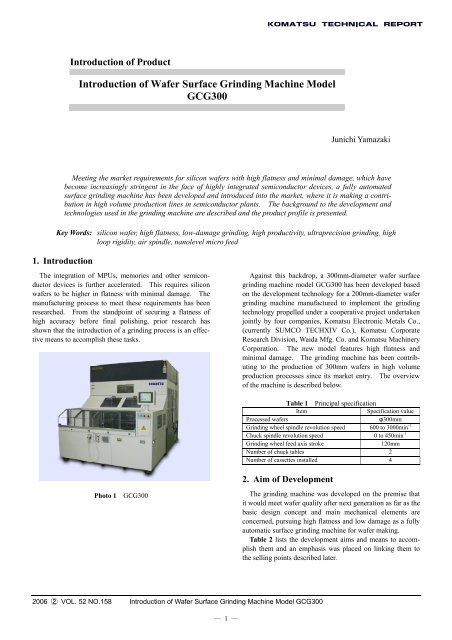
Introduction of Wafer Surface Grinding Machine Model ... - Komatsu
Introduction of Wafer Surface Grinding Machine Model ... - Komatsu
Introduction of Wafer Surface Grinding Machine Model ... - Komatsu

You also want an ePaper? Increase the reach of your titles
YUMPU automatically turns print PDFs into web optimized ePapers that Google loves.
<strong>Introduction</strong> <strong>of</strong> Product<br />
<strong>Introduction</strong> <strong>of</strong> <strong>Wafer</strong> <strong>Surface</strong> <strong>Grinding</strong> <strong>Machine</strong> <strong>Model</strong><br />
GCG300<br />
Junichi Yamazaki<br />
Meeting the market requirements for silicon wafers with high flatness and minimal damage, which have<br />
become increasingly stringent in the face <strong>of</strong> highly integrated semiconductor devices, a fully automated<br />
surface grinding machine has been developed and introduced into the market, where it is making a contribution<br />
in high volume production lines in semiconductor plants. The background to the development and<br />
technologies used in the grinding machine are described and the product pr<strong>of</strong>ile is presented.<br />
Key Words: silicon wafer, high flatness, low-damage grinding, high productivity, ultraprecision grinding, high<br />
loop rigidity, air spindle, nanolevel micro feed<br />
1. <strong>Introduction</strong><br />
The integration <strong>of</strong> MPUs, memories and other semiconductor<br />
devices is further accelerated. This requires silicon<br />
wafers to be higher in flatness with minimal damage. The<br />
manufacturing process to meet these requirements has been<br />
researched. From the standpoint <strong>of</strong> securing a flatness <strong>of</strong><br />
high accuracy before final polishing, prior research has<br />
shown that the introduction <strong>of</strong> a grinding process is an effective<br />
means to accomplish these tasks.<br />
Against this backdrop, a 300mm-diameter wafer surface<br />
grinding machine model GCG300 has been developed based<br />
on the development technology for a 200mm-diameter wafer<br />
grinding machine manufactured to implement the grinding<br />
technology propelled under a cooperative project undertaken<br />
jointly by four companies, <strong>Komatsu</strong> Electronic Metals Co.,<br />
(currently SUMCO TECHXIV Co.), <strong>Komatsu</strong> Corporate<br />
Research Division, Waida Mfg. Co. and <strong>Komatsu</strong> <strong>Machine</strong>ry<br />
Corporation. The new model features high flatness and<br />
minimal damage. The grinding machine has been contributing<br />
to the production <strong>of</strong> 300mm wafers in high volume<br />
production processes since its market entry. The overview<br />
<strong>of</strong> the machine is described below.<br />
Photo 1<br />
GCG300<br />
Table 1 Principal specification<br />
Item<br />
Specification value<br />
Processed wafers<br />
φ300mm<br />
<strong>Grinding</strong> wheel spindle revolution speed 600 to 3000min -1<br />
Chuck spindle revolution speed 0 to 450min -1<br />
<strong>Grinding</strong> wheel feed axis stroke<br />
120mm<br />
Number <strong>of</strong> chuck tables 2<br />
Number <strong>of</strong> cassettes installed 4<br />
2. Aim <strong>of</strong> Development<br />
The grinding machine was developed on the premise that<br />
it would meet wafer quality after next generation as far as the<br />
basic design concept and main mechanical elements are<br />
concerned, pursuing high flatness and low damage as a fully<br />
automatic surface grinding machine for wafer making.<br />
Table 2 lists the development aims and means to accomplish<br />
them and an emphasis was placed on linking them to<br />
the selling points described later.<br />
2006 2 VOL. 52 NO.158 <strong>Introduction</strong> <strong>of</strong> <strong>Wafer</strong> <strong>Surface</strong> <strong>Grinding</strong> <strong>Machine</strong> <strong>Model</strong> GCG300<br />
― 1 ―
Table 2 Development aims and means to accomplish them<br />
Development aim<br />
Means for accomplishment<br />
1) High flatness<br />
grinding<br />
“Low thermal<br />
displacement”<br />
• Low overall height by lateral processing<br />
unit<br />
• High rigidity and high precision air<br />
spindle and low heat generation by<br />
main shaft cooling<br />
2) Low-damage<br />
grinding<br />
3) High productivity<br />
“Flatness adjustment”<br />
• Independent adjustment <strong>of</strong> declinations<br />
<strong>of</strong> grinding wheel spindle and<br />
chuck spindle<br />
• Original chuck<br />
“Retention <strong>of</strong><br />
high flatness”<br />
“Low vibration” • Static air pressure used in grinding<br />
wheel and chuck spindles<br />
“High rigidity” • High loop rigidity <strong>of</strong> grinding wheel<br />
and wafer holding systems<br />
“Micro feeding” • High precision micro feeding <strong>of</strong><br />
“<strong>Grinding</strong><br />
wheel”<br />
“System”<br />
“IT”<br />
nanolevel<br />
• R&D in cooperation with a grinding<br />
wheel manufacturer<br />
• Both side processing by two heads in<br />
left and right direction + Transfer<br />
robot<br />
• Status display, collection <strong>of</strong> control<br />
data and communication<br />
cooling mechanism, enabling operation with low heat generation.<br />
The grinding wheel and chuck <strong>of</strong> the grinding machine are<br />
shown below. (Photo 2)<br />
1) Processing accuracy (Source: Test data <strong>of</strong> <strong>Komatsu</strong> machinery<br />
Corporation)<br />
Thickness<br />
Number <strong>of</strong> wafers processed<br />
Fig. 1 Thickness dispersion<br />
1µm<br />
“Selling Points”<br />
Features by high flatness grinding:<br />
• Small fluctuations <strong>of</strong> flatness on entire wafer surfaces<br />
(GBIR)<br />
• High shape controllability<br />
• High flatness <strong>of</strong> chip size at sites (SFQR)<br />
Feature by low-damage grinding:<br />
• Small polishing removal in post-process<br />
High productivity achieved through these features<br />
3. Principal Features<br />
3.1 High Flatness <strong>Grinding</strong><br />
<strong>Komatsu</strong>’s unique lateral processing unit structure is<br />
adopted as a means to enable high flatness grinding, achieving<br />
a high rigidity and low thermal displacement. A high<br />
and stable flatness is achieved in continuous processing also.<br />
Both the grinding wheel spindle and chuck spindle adopt<br />
high accuracy air spindles and incorporate a main spindle<br />
Flatness GBIR<br />
Number <strong>of</strong> wafers processed<br />
0.2µm<br />
Number <strong>of</strong> wafers processed<br />
Fig. 2 Flatness GBIR (300mm diameter) dispersion<br />
Flatness SFQR<br />
Fig. 3 Flatness SFQR (25mm square)<br />
GBIR (AS GRIND)<br />
Chuck<br />
spindle<br />
Photo 2 GCG300 grinding wheel and chuck<br />
<strong>Grinding</strong><br />
wheel<br />
GBIR[um]<br />
2<br />
Conventional<br />
1.8<br />
<strong>Grinding</strong> machine<br />
1.6<br />
GCG300<br />
1.4<br />
1.2<br />
1<br />
0.8<br />
0.2µm<br />
0.6<br />
0.4<br />
0.2<br />
0<br />
1 6 11 16 21 26 31 36 41 46 51 56 61 66 71 76 81 86 91 96<br />
<strong>Wafer</strong> No.<br />
Fig. 4 Variations <strong>of</strong> flatness GBIR (300mm diameter)<br />
2006 2 VOL. 52 NO.158 <strong>Introduction</strong> <strong>of</strong> <strong>Wafer</strong> <strong>Surface</strong> <strong>Grinding</strong> <strong>Machine</strong> <strong>Model</strong> GCG300<br />
― 2 ―
Dispersions <strong>of</strong> processing accuracy for both thickness (Fig.<br />
1) and flatness GBIR/300mm diameter (Fig. 2) are small and<br />
flatness SFQR (Fig. 3) <strong>of</strong> the chip size at sites is good.<br />
Recently, flatness is enhanced further through R&D <strong>of</strong><br />
grinding wheel. Figure 4 shows that flatness immediately<br />
after starting machine operation is very stable, indicating that<br />
low thermal displacement, which is a feature <strong>of</strong> the lateral<br />
processing unit, is demonstrated.<br />
Next, the technologies that make this high flatness grinding<br />
feasible are described in detail.<br />
2) Means to accomplish high flatness grinding<br />
(1) Low overall height by lateral processing unit<br />
A unique lateral processing unit structure is adopted with<br />
this machine by reducing the height <strong>of</strong> the processing unit to<br />
ensure dynamic and thermal stability. This has achieved a<br />
high rigidity and low thermal displacement, making a stable,<br />
high flatness in continuous processing also.<br />
Air spindle for<br />
grinding wheel<br />
<strong>Grinding</strong><br />
wheel<br />
<strong>Wafer</strong><br />
Chuck<br />
table Air spindle<br />
for chuck<br />
and cooling <strong>of</strong> the motor outer casing keep thermal displacement<br />
low.<br />
(3) Independent adjustment <strong>of</strong> declinations <strong>of</strong> grinding wheel<br />
spindle and chuck spindle<br />
The wafer is processed by the infeed grinding method<br />
whereby the wafer is chucked onto the chuck and the grinding<br />
wheel spindle installed opposite the chuck is slowly<br />
moved to the wafer side, to grind the wafer to the desired<br />
thickness.<br />
The position relations between the grinding wheel and<br />
wafer are illustrated in Fig. 7. The grinding wheel spindle<br />
is slightly tilted against the chuck. As adjustment before<br />
processing the wafer, the chuck table surfaces are self-cut by<br />
the grinding wheel for chucking so that the surfaces are<br />
slightly bumped. Thus, the portion <strong>of</strong> a wafer that is processed<br />
at a random point during processing is the “grinding<br />
length” part from the periphery <strong>of</strong> the wafer to the center <strong>of</strong><br />
it as illustrated. Contact <strong>of</strong> the grinding wheel with the<br />
wafer in this area determines the processing accuracy.<br />
Top view<br />
<strong>Grinding</strong><br />
wheel<br />
+<br />
-<br />
Fig. 5 Lateral processing unit<br />
(2) High rigidity, high precision air spindle and main<br />
spindle cooling<br />
Large porous air bearings are adopted in the grinding<br />
wheel and chuck spindles, assuring a high rigidity. The<br />
rotating main spindles are levitated by air and are supported<br />
contactless, providing high speed and high precision revolutions.<br />
Fig. 6 <strong>Grinding</strong> wheel and a wafer after processing<br />
The spindle on the grinding wheel is driven by a built-in<br />
motor. Low heat conduction material between the bearing<br />
<strong>Grinding</strong><br />
length<br />
<strong>Wafer</strong><br />
(Chucked to chuck)<br />
<strong>Grinding</strong><br />
wheel head<br />
Side view<br />
Fig. 7 Flatness adjusting mechanism<br />
Chuck head<br />
The position relationship between the grinding wheel and<br />
the wafer is very important for ultrahigh precision grinding<br />
<strong>of</strong> a wafer. Due to a difference in the processing loads<br />
caused when self-cutting the surface <strong>of</strong> the chuck table before<br />
processing a wafer and then grinding a wafer, the difference<br />
is produced in the wafer shape in relation to the<br />
chuck if the position relationship is maintained as is, failing<br />
to produce an adequate flatness and necessitating spindle<br />
adjustment. The grinding wheel head and chuck head <strong>of</strong><br />
the GCG300 have independent spindle adjusting mechanisms.<br />
As shown in Fig. 8, the wafer surface bump quantity is adjusted<br />
by adjusting the grinding wheel spindle declination<br />
and the linearity from the periphery to the center <strong>of</strong> a wafer<br />
is adjusted by chuck spindle declination adjustment, both<br />
independently. This mechanism allows easy control <strong>of</strong> the<br />
shape and high mechanical rigidity, resulting in a good repeatability<br />
and short adjusting time.<br />
+<br />
-<br />
2006 2 VOL. 52 NO.158 <strong>Introduction</strong> <strong>of</strong> <strong>Wafer</strong> <strong>Surface</strong> <strong>Grinding</strong> <strong>Machine</strong> <strong>Model</strong> GCG300<br />
― 3 ―
<strong>Grinding</strong> wheel spindle<br />
declination: Every 1µm<br />
Chuck spindle declination:<br />
Every 1µm<br />
Fig. 8 Control <strong>of</strong> wafer shape by spindle adjustment<br />
(4) Original chuck<br />
Recently, flatness is demanded maximally to the very limit<br />
<strong>of</strong> the wafer periphery to increase the wafer yield. For this<br />
reason, roll-<strong>of</strong>f <strong>of</strong> wafer edges needs to be reduced. A<br />
chuck has been developed hardly causing leak during<br />
chucking so that the wafer can be chucked correctly up to its<br />
periphery and allowing flat processing to the periphery <strong>of</strong> the<br />
chucked wafer even if the chuck is self-cut.<br />
By using this original chuck, wafer edge roll-<strong>of</strong>f could be<br />
reduced and flatness SFQR could be improved.<br />
Figures 9 and 10 show edge roll-<strong>of</strong>f and shapes <strong>of</strong><br />
chucked wafers. Chucking by a conventional chuck produced<br />
large roll-<strong>of</strong>f <strong>of</strong> wafer edges and the wafer is wavy.<br />
On the other hand, the original chuck produced slight roll-<strong>of</strong>f<br />
<strong>of</strong> wafer edges and the wafer was chucked correctly along<br />
the chuck pr<strong>of</strong>ile, producing no waviness.<br />
Before: Imperfect chucking<br />
Original chuck: Perfect chucking<br />
Fig. 9 <strong>Wafer</strong> edge roll-<strong>of</strong>f<br />
3.2 Low-Damage <strong>Grinding</strong><br />
Flatness and “damageless” are the quality requirements<br />
that are ultimately required on semiconductor wafers.<br />
Damage to wafers can be removed perfectly only by the final<br />
process <strong>of</strong> the wafer making process, namely, polishing.<br />
The polishing process has a low processing rate, but has no<br />
shape creating ability. Therefore, the polishing removal<br />
must be reduced to mitigate the load to the polishing system<br />
and to maintain the shape created during grinding. The<br />
wafer grinding process before polishing should avoid inflicting<br />
damage on the wafer as best as possible.<br />
1) Means to accomplish low-damage grinding<br />
The most ideal low-damage grinding method is ductility<br />
mode grinding illustrated on the right <strong>of</strong> Fig. 11. Shown on<br />
the left is an example <strong>of</strong> grinding in the brittleness mode,<br />
which is the usual grinding method, and damage remains<br />
deep. Ductility mode grinding can be accomplished by<br />
controlling to stabilize the grinding wheel cross feed to less<br />
than Dc (critical penetration depth for fracture initiation),<br />
which corresponds to about 0.1µm with silicon wafers.<br />
In other words, ds must be ds < Dc ≒ 0.1µm<br />
Abrasive grain<br />
<strong>Wafer</strong><br />
<strong>Grinding</strong><br />
damage<br />
d L >d S<br />
d L<br />
Fig. 11 Image <strong>of</strong> grinding mechanism<br />
Low-damage grinding by ductility mode processing can be<br />
accomplished by:<br />
“Low vibration” • Static air pressure adopted in grinding<br />
wheel and chuck spindle<br />
“High rigidity” • High loop rigidity <strong>of</strong> grinding wheel<br />
and wafer holding systems<br />
“Micro feeding” • High precision micro feeding <strong>of</strong><br />
nanolevel<br />
The motion accuracy <strong>of</strong> a nanometer order based on the<br />
motion transfer principle produces a modified work damage<br />
layer with extremely scant damage.<br />
The structure <strong>of</strong> the grinding machine has been developed<br />
with the configuration illustrated in Fig. 12 to realize this<br />
ductility mode.<br />
Air spindle for<br />
grinding wheel<br />
<strong>Wafer</strong><br />
Air spindle for<br />
chuck<br />
Before: Imperfect chucking<br />
Original chuck: Perfect<br />
chucking<br />
High loop<br />
rigidity<br />
Micro feeding<br />
<strong>of</strong> nanolevel<br />
Fig. 10 Shapes <strong>of</strong> chucked wafers<br />
Fig. 12 <strong>Machine</strong> configuration for low-damage grinding<br />
2006 2 VOL. 52 NO.158 <strong>Introduction</strong> <strong>of</strong> <strong>Wafer</strong> <strong>Surface</strong> <strong>Grinding</strong> <strong>Machine</strong> <strong>Model</strong> GCG300<br />
― 4 ―
2) R&D in cooperation with grinding wheel manufacturer<br />
To further eliminate damage to achieve low-damage<br />
grinding, R&D <strong>of</strong> a super fine grinding wheel that uses abrasive<br />
grains less than 1µm in size is undertaken jointly with<br />
an abrasive manufacturer.<br />
TEM observations <strong>of</strong> damage after grinding using a conventional<br />
grinding wheel and super fine grinding wheel are<br />
shown in Fig. 13. The damage depth has been reduced to<br />
about 1/5. Optimization will be pursued further such as<br />
optimizing processing conditions.<br />
Fig. 13 Results <strong>of</strong> TEM observations<br />
3.3 High productivity<br />
1) High throughput system<br />
The system illustrated in Fig. 14 operates as follows.<br />
Processing<br />
Chamber L<br />
Conventional<br />
grinding wheel<br />
<strong>Grinding</strong><br />
wheel<br />
Unit L<br />
Chuck<br />
Super fine grain<br />
grinding wheel<br />
Super fine grain<br />
grinding wheel<br />
Articulated<br />
Robot A<br />
<strong>Grinding</strong><br />
surface<br />
<strong>Grinding</strong><br />
wheel<br />
Unit R<br />
5 3<br />
Chuck<br />
Processing<br />
Chamber R<br />
(1) Robot B picks up a wafer from a cassette and mounts it<br />
on the prewashing unit.<br />
(2) A brush washes the surface <strong>of</strong> a wafer, which will be<br />
chucked by the chuck. The surface <strong>of</strong> the wafer is<br />
then dried by air blowing.<br />
(3) Robot A transfers the wafer from the prewashing unit to<br />
Processing Chamber R. Side 1 is processed.<br />
(4) The processed side (the side to be chucked in the next<br />
process in Processing Chamber L) is washed.<br />
(5) Robot A transfers the wafer to Processing Chamber L<br />
for processing on Side 2.<br />
(6) After processing, Robot A transfers the wafer to the<br />
post-washing unit. The wafer after processing is<br />
washed with water and is dried by spinning.<br />
(7) Robot B stores a wafer, whose both sides are processed,<br />
in a cassette.<br />
2) Enhanced production efficiency by IT<br />
(1) Stable wafer quality and preventive maintenance <strong>of</strong><br />
system<br />
• By locally connecting the GCG300 to a PC for data<br />
collection, analysis <strong>of</strong> trends such as the amount <strong>of</strong><br />
grinding wheel wear, chuck suction pressure, quantity<br />
<strong>of</strong> grinding water and motor current can be performed,<br />
thereby contributing to the stable production <strong>of</strong> wafers.<br />
(2) Production control<br />
• By connecting the GCG300 to a host PC by a network,<br />
lot Nos., contents in a cassette, processing recipes, system<br />
IDs and other indication data, as well as processing<br />
start time, grinding wheel current, amount <strong>of</strong> grinding<br />
wheel wear, thicknesses before and after processing<br />
and other processing data are sent. The communication<br />
protocol is SEMI standard (GEM) compatible.<br />
(3) Enhanced system operability (Shorter downtime)<br />
• The data collection PC is remotely accessed through<br />
the Internet or through an internal circuit (VPN - virtual<br />
private network) to allow operation just like by the<br />
operation panel supplied with the system as an accessory,<br />
thereby facilitating failure cause analysis and resetting.<br />
The control circuit can be edited and updated<br />
allowing direct interaction with the production site,<br />
thereby reducing downtime to a minimum.<br />
Stable wafer quality and preventive maintenance <strong>of</strong> system<br />
6<br />
4<br />
2<br />
Local<br />
connection<br />
Post-washing<br />
unit<br />
For data collection<br />
C1<br />
7<br />
Scalar Robot<br />
B<br />
1<br />
C2 C3 C4<br />
Cassette x4<br />
Fig. 14 System<br />
Prewashing unit<br />
GCG300<br />
Production control<br />
Host PC<br />
(1) Internet<br />
(2) Internal circuit (VPN)<br />
Remote accessing<br />
Communication protocol is SEMI standard (GEM)<br />
Higher system throughput<br />
(Shorter downtime)<br />
Fig. 15 Enhanced production efficiency by IT<br />
2006 2 VOL. 52 NO.158 <strong>Introduction</strong> <strong>of</strong> <strong>Wafer</strong> <strong>Surface</strong> <strong>Grinding</strong> <strong>Machine</strong> <strong>Model</strong> GCG300<br />
― 5 ―
4. Conclusion<br />
<strong>Grinding</strong> machine<br />
High accuracy<br />
High rigidity<br />
High resolution feed<br />
S<strong>of</strong>tware/expertise<br />
• <strong>Wafer</strong> washing<br />
• Thickness control<br />
<strong>Introduction</strong> <strong>of</strong> the writer<br />
Junichi Yamazaki<br />
Entered <strong>Komatsu</strong> in 1982.<br />
Currently assigned to the Electronics Development<br />
Office, Electronics Division,<br />
<strong>Komatsu</strong> <strong>Machine</strong>ry Corporation.<br />
S<strong>of</strong>tware/expertise<br />
• <strong>Grinding</strong> conditions<br />
• Truing<br />
<strong>Grinding</strong> wheel<br />
Low damage<br />
Long life<br />
High efficiency grinding<br />
High flatness<br />
Low damage<br />
Low cost<br />
Fig. 16 Total solutions<br />
S<strong>of</strong>tware/expertise<br />
• Chuck washing<br />
• Self cutting<br />
Chuck<br />
High precision chucking<br />
mechanism<br />
Quality <strong>of</strong> chucking surface<br />
The GCG300 is a grinding machine featuring high accuracy<br />
and high rigidity pursued hand in hand with the technological<br />
capability <strong>of</strong> a machine tool manufacturer. The joint<br />
development <strong>of</strong> a grinding wheel with a leading tool manufacturer<br />
has enabled the use <strong>of</strong> an optimum grinding wheel<br />
that has a wide application scope and that matches the user<br />
needs.<br />
A chuck that is unique to the GCG300 suiting high flatness<br />
grinding is installed.<br />
The GCG300 responds to the needs <strong>of</strong> the customer with<br />
total solutions for the wafer grinding technology with a focus<br />
on the grinding machines.<br />
[A few words from the writers]<br />
<strong>Komatsu</strong> <strong>Machine</strong>ry Corporation specializes in machine tools,<br />
mainly machines for engine crank shafts, and is engaged in the<br />
machine tool business. Parallel with the machine tool business,<br />
<strong>Komatsu</strong> <strong>Machine</strong>ry Corporation produces and sells semiconductor<br />
production equipment and liquid crystal manufacturing<br />
systems as electronic business. In the area <strong>of</strong> semiconductor<br />
production equipment, the Company has been manufacturing<br />
silicon single crystal pulling systems for many years. The<br />
Company has been facing the task <strong>of</strong> introducing a product into<br />
the market in the semiconductor wafer production process as a<br />
next mainstay product. The wafer surface grinding machine<br />
model GCG300 described above has been developed and introduced<br />
to the market, contributing to production by high volume<br />
production processes. The business environment <strong>of</strong> semiconductors<br />
is facing great changes at present. However, this situation<br />
will be seized as a business opportunity and these changes<br />
will be fed back to product development to ensure further<br />
growth <strong>of</strong> our business.<br />
2006 2 VOL. 52 NO.158 <strong>Introduction</strong> <strong>of</strong> <strong>Wafer</strong> <strong>Surface</strong> <strong>Grinding</strong> <strong>Machine</strong> <strong>Model</strong> GCG300<br />
― 6 ―