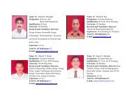
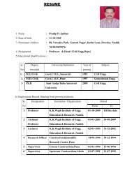
Prof. Dr. Preeti Dinesh Bhamre 2. Date of birth - K. K. Wagh ...
Prof. Dr. Preeti Dinesh Bhamre 2. Date of birth - K. K. Wagh ...
Prof. Dr. Preeti Dinesh Bhamre 2. Date of birth - K. K. Wagh ...

Create successful ePaper yourself
Turn your PDF publications into a flip-book with our unique Google optimized e-Paper software.
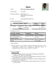
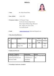
RESUME<br />
1. Name : <strong>Pr<strong>of</strong></strong>. <strong>Dr</strong>. <strong>Preeti</strong> <strong>Dinesh</strong> <strong>Bhamre</strong><br />
<strong>2.</strong> <strong>Date</strong> <strong>of</strong> <strong>birth</strong> : 29-11-1973.<br />
3. Office Address : Dept. <strong>of</strong> Information Technology,<br />
K.K.<strong>Wagh</strong> Institute <strong>of</strong> Engg. Education and Research, Nasik<br />
Panchavati, Amrutdham, Nasik -422003<br />
Tel: (O) (0253) 2221271, 2512867<br />
4. Email : preetibhamre@yahoo.com / patilpb@ee.iitb.ac.in .<br />
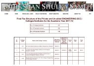
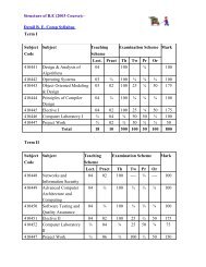
5. Educational Qualifications :<br />
Sr.<br />
No.<br />
University /<br />
Institute<br />
Degree Year Field <strong>of</strong><br />
Specialization<br />
1 Govt. College B.E<br />
<strong>of</strong> Engg., E/TC<br />
Pune<br />
2 Govt. College<br />
<strong>of</strong> Engg.,<br />
Pune<br />
3 Indian<br />
Institute <strong>of</strong><br />
Technology,<br />
Bombay<br />
M.E<br />
E/TC<br />
Ph.D.<br />
(Under the guidance <strong>of</strong><br />
<strong>Pr<strong>of</strong></strong>.<strong>Dr</strong>.R.K.Shevgaonkar,<br />
Former Vice Chancellor,<br />
Pune University and<br />
currently Director IIT,<br />
Delhi)<br />
Class<br />
Obtained<br />
1995 - First class<br />
(61%)<br />
2001 Instrumentation<br />
and Controls<br />
2012 Photonic Crystal<br />
Devices (Optical<br />
Communication )<br />
Distn.<br />
(71%)<br />
CGPA – 9.0<br />
6. Employment Record:<br />
University / Employer Designation Period<br />
K. K.<strong>Wagh</strong> Institute <strong>of</strong> Engineering<br />
Education and Research, Nasik<br />
Head, I.T. Dept and<br />
<strong>Pr<strong>of</strong></strong>essor in Electronics<br />
From 1 st Dec. 2010 till<br />
date<br />
K. K.<strong>Wagh</strong> Institute <strong>of</strong> Engineering<br />
Education and Research, Nasik<br />
K.K.<strong>Wagh</strong> Women’s Polytechnic,<br />
Nashik<br />
K. K.<strong>Wagh</strong> Institute <strong>of</strong> Engineering<br />
Education and Research, Nasik<br />
Cummins College <strong>of</strong> Engg., Pune<br />
Engg.<br />
Head, I.T. Dept and<br />
Assistant <strong>Pr<strong>of</strong></strong>essor in<br />
Electronics Engg.<br />
July 2009 to Dec 2010<br />
I/C Principal Mar 2005 to July 2009<br />
Lecturer in Electronic<br />
Engg.<br />
Lecturer in Electronic<br />
Engg.<br />
Aug 1996 to Mar 2005<br />
Aug 1995-June 1996.<br />
Other Responsibilities Handled:<br />
1) Nominated on the “Learning Resource Selection Committee”, YCMOU, Nasik in<br />
Feb. 2013.<br />
2) Worked as Member <strong>of</strong> Committee for Design <strong>of</strong> Curriculum <strong>of</strong> Computer Courses,<br />
YCMOU, Nasik
3) Worked as a Visiting Faculty for two subjects for the Post Graduate students <strong>of</strong><br />
PGDM II (IT) in Symbiosis College (SCHMRD), Nashik during Sept. 2003 to Jan<br />
2004 and Sept. 2004 to Dec 2004.<br />
4) Worked as Student Branch Counselor and Managing Committee Member for CSI<br />
Nashik Chapter during the period 2002-2005.<br />
5) Member <strong>of</strong> Local Managing Committee <strong>of</strong> K. K. <strong>Wagh</strong> Institute <strong>of</strong> Engineering<br />
Education and Research, Nasik<br />
7. Articles Published:<br />
[1] “Storage Area Networks”, CSI Communications, Dec. 2003., ISSN-0970-647X<br />
[2] “Sequence Detector”, published in Lab Experiments Journal, Vol-4, No-1,<br />
March 2004, ISSN-0972-6055-KARENG/2001/8386<br />
8. Journal Publications:<br />
[1] <strong>Preeti</strong>. B. Patil (<strong>Bhamre</strong>), Sarang Pendharker and R. K. Shevgaonkar,<br />
“Electrical Modeling <strong>of</strong> Photonic Crystal Defects,” Microwave and Optical<br />
Technol. Lett., vol. 54, No. 11, pp.2523-2528, Nov. 201<strong>2.</strong><br />
[2] P. B. Patil (<strong>Bhamre</strong>), R. K. Shevgaonkar, “Improved S-parameter Model for<br />
Photonic Crystal Defects”, SPIE Select Proc. – Vol 8173, 8173E, 2010<br />
[3] P. B. Patil (<strong>Bhamre</strong>), R. K. Shevgaonkar, “Electrical modeling <strong>of</strong> single defect<br />
in photonic crystal waveguide”, SPIE Select Proc. – Vol 7138, pp214-219, 2008,<br />
9. Conference Publications: 12 National /International Conferences<br />
[1] P. B. Patil(<strong>Bhamre</strong>), R. K. Shevgaonkar, “Numerical Analysis <strong>of</strong> Propagation in<br />
Finite Length 2-D Photonic Crystal Waveguide with Single Defect”, Proc. <strong>of</strong><br />
International Conference on Microwaves and Optoelectronics, <strong>Dr</strong>. Babasaheb<br />
Ambedkar Marathwada University, Aurangabad, (Dec. 2007).<br />
[2] P. B. Patil(<strong>Bhamre</strong>), R. K. Shevgaonkar, “Photonic Crystal Devices for<br />
Communication”, (Invited Paper), Proc.<strong>of</strong> National Workshop on Advanced<br />
Optoelectronic Materials and Devices, Benaras Hindu University, (Dec 2007).<br />
[3] P. B. Patil(<strong>Bhamre</strong>), R. K. Shevgaonkar, “Analysis <strong>of</strong> a finite length 2-D<br />
photonic crystal waveguide”, Proc. <strong>of</strong> National Conference on Communications,<br />
I.I.T., Bombay, 324-326, (Feb. 2008).<br />
[4] P. B. Patil(<strong>Bhamre</strong>), R. K. Shevgaonkar, “Electrical modeling <strong>of</strong> single defect in<br />
photonic crystal waveguide”, SPIE Proc. <strong>of</strong> 6 th International Conference on<br />
Photonics, Devices and Systems, Prague, Czech Rep., (Aug. 2008)<br />
[5] P. B. Patil, R. K. Shevgaonkar, “Spectral Characteristics <strong>of</strong> Defects in Photonic<br />
Crystals”, 9 th International Conference on Fiber Optics and Photonics,<br />
Photonics 2008, IIT Delhi, (Dec. 2008).<br />
[6] P. B. Patil(<strong>Bhamre</strong>), R. K. Shevgaonkar, “Photonic Crystal Devices for All<br />
Optical Communication Systems”, (Invited Paper), 9 th International Conference<br />
on Fiber Optics and Photonics, Photonics 2008, IIT Delhi, (Dec. 2008).<br />
[7] P. B. Patil(<strong>Bhamre</strong>), R. K. Shevgaonkar, “Electrical Modeling <strong>of</strong> a defect in<br />
Photonic Crystal Waveguide,” IEEE Proc. <strong>of</strong> the 6 th IEEE International<br />
Conference on Wireless and Optical Communication Networks, WOCN 2009,<br />
Cairo, Egypt, April. 2009.
[8] Sarvagya Dwivedi, P. B. Patil(<strong>Bhamre</strong>), R. K. Shevgaonkar, “ Polar Grid<br />
Microstructured Fiber Raman Amplifier”, Proc. <strong>of</strong> 12 th International Symposium<br />
and Microwave and Optical Technology, ISMOT 2009, University <strong>of</strong> Delhi and<br />
University <strong>of</strong> Nevada, Reno, USA, December 16-19, 2009.<br />
[9] P. B. Patil(<strong>Bhamre</strong>), R. K. Shevgaonkar, “Spectral Characteristics <strong>of</strong> Multiple<br />
Defects in a Photonic Crystal Waveguide,” IEEE Proc. <strong>of</strong> 7 th IEEE Intl. Conf.<br />
on Wireless and Optical Communications Networks (Next Generation Internet),<br />
WOCN2010, Colombo, Sri Lanka, Sept. 2010<br />
[10] P. B. Patil(<strong>Bhamre</strong>), R. K. Shevgaonkar, “Improved S-parameter Model for<br />
Photonic Crystal Defects”, Proc. <strong>of</strong> 10 th International Conference on Fiber<br />
Optics and Photonics, Photonics 2010, IIT Guwahati, (Dec. 2010).<br />
[11]<strong>Preeti</strong> B. Patil(<strong>Bhamre</strong>), “Photonic Crystal Devices for All Optical<br />
Communication Systems”, Proc. <strong>of</strong> IEI Annual Technical Paper Meet, Pune,<br />
Nov. 2011.<br />
[12] <strong>Preeti</strong> D. <strong>Bhamre</strong> and R. K. Shevgaonkar, “Design <strong>of</strong> 2D Photonic Crystal<br />
Waveguide based Bandpass Filter using Electrical Models <strong>of</strong> a Defect,” OSA<br />
Technical Digest 10 th Intl. Conf. on Fiber optics and Photonics, India, 201<strong>2.</strong><br />
10. Awards:<br />
1) SPIE Student Best Paper Award at 6 th International Conference on Photonics,<br />
Devices and Systems, Prague, Czech Republic (Aug. 2008)<br />
2) <strong>Pr<strong>of</strong></strong>. B. B. Deshpande Prize for Best Paper at the Annual Technical Paper<br />
Meet-2011 organized by The Institute <strong>of</strong> Engineers (India) Pune (Nov. 2011)<br />
3) Lady Engineer’s Award by The Institute <strong>of</strong> Engineers (India) Nashik Chapter<br />
(Sept. 2012)<br />
11. Areas <strong>of</strong> Interest: Fibre Optic Communication, Photonics, Non-linear fibre optics<br />
1<strong>2.</strong> Hobbies and Other Achievements: Kathak Dance Performer<br />
‣ Visharad/Bachelor degree in Kathak Dance.<br />
‣ Won First prize for Kathak Dance at All India Dance Competition Organized by<br />
Sur Singar, Bombay.<br />
‣ Kathak Dance performance on Doordarshan in March 1989 and various other<br />
performances in Delhi, Bombay, Pune, Madhya Pradesh, Nashik etc.