Intel PXA250 and PXA210 Applications Processors
Intel PXA250 and PXA210 Applications Processors Intel PXA250 and PXA210 Applications Processors
Power and Clocking Note: If Hardware Reset is entered during Sleep Mode, the proper power-supply stabilization times and nRESET timing requirements indicated in Table 8-7, “Power-On Timing Specifications” on page 8-12 must be observed. Figure 8-1. Power-On Reset Timing t R_VCCQ VCCQ, PWR_EN t R_VCCN VCCN VCC nTRST t D_VCCN t D_VCC t R_VCC t D_NTRST t D_JTAG JTAG PINS nRESET t D_NRESET nRESET_OUT t D_OUT Note: nBATT_FAULT and nVDD_FAULT must be high before nRESET_OUT is deasserted or PXA250 enters Sleep Mode Table 8-7. Power-On Timing Specifications Symbol Description Min Typical Max t R_VCCQ VCCQ Rise / Stabilization time 0.01 ms — 100 ms t R_VCCN VCCN Rise / Stabilization time 0.01 ms — 100 ms t R_VCC VCC, PLL_VCC Rise / Stabilization time 0.01 ms — 10 ms t D_VCCN Delay between VCCQ stable and VCCN applied 0ms — — t D_VCC Delay from VCCN stable and VCC, PLL_VCC applied 0ms — — t D_NTRST Delay between VCC, PLL_VCC stable and nTRST deasserted 50 ms — — t D_JTAG t D_NRESET t D_OUT Delay between nTRST deasserted and JTAG pins active, with nRESET asserted Delay between VCC, PLL_VCC stable and nRESET deasserted Delay between nRESET deasserted and nRESET_OUT deasserted 0.03 ms — — 50 ms — — 18.1 ms — 18.2 ms 8.5.3 Hardware Reset Timing The timing sequences shown in Figure 8-2 “Hardware Reset Timing” assumes the power supplies are stable at the assertion of nRESET. If the power supplies are unstable, follow the timings indicated in Section 8.5.2, “Power On Timing” on page 11. 8-12 PXA250 and PXA210 Applications Processors Design Guide
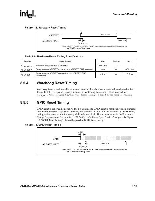
Power and Clocking Figure 8-2. Hardware Reset Timing nRESET nRESET_OUT t DHW_NRESET t DHW_OUT t DHW_OUT_A Note: nBATT_FAULT and nVDD_FAULT must be high before nRESET is deasserted or PXA250 enters Sleep Mode Table 8-8. Hardware Reset Timing Specifications Symbol Description Min Typical Max t DHW_NRESET Minimum assertion time of nRESET 0.001 ms — — t DHW_OUT_A Delay between nRESET Asserted and nRESET_OUT Asserted 0ms — 0.001 ms t DHW_OUT Delay between nRESET deasserted and nRESET_OUT deasserted 18.1 ms — 18.2 ms 8.5.4 Watchdog Reset Timing Watchdog Reset is an internally generated reset and therefore has no external pin dependencies. The nRESET_OUT pin is the only indicator of Watchdog Reset, and it stays asserted for t DHW_OUT . Refer to Figure 8-2, “Hardware Reset Timing” on page 8-13 for more information. 8.5.5 GPIO Reset Timing GPIO Reset is generated externally. The pin used as the GPIO Reset is reconfigured as a standard GPIO after the reset propagates internally. Because the clock module is not reset by GPIO Reset, timing varies based on the frequency of the selected clock. Timing also varies in the Frequency Change Sequence (see Section 8.4.1, “32.768 kHz Oscillator Specifications” on page 4). Figure 8-3 “GPIO Reset Timing” shows the possible GPIO Reset timing. Figure 8-3. GPIO Reset Timing t A_GP[1] GP[1] nRESET_OUT t DGP_OUT t DGP_OUT_A Note: nBATT_FAULT and nVDD_FAULT must be high before nRESET is deasserted or PXA250 enters Sleep Mode PXA250 and PXA210 Applications Processors Design Guide 8-13
- Page 29 and 30: System Memory Interface Table 2-1.
- Page 31 and 32: . System Memory Interface 2.4 SDRAM
- Page 33 and 34: System Memory Interface Table 2-4.
- Page 35 and 36: System Memory Interface Table 2-6.
- Page 37 and 38: System Memory Interface Table 2-8.
- Page 39 and 40: System Memory Interface Figure 2-5.
- Page 41 and 42: System Memory Interface Figure 2-6.
- Page 43 and 44: System Memory Interface 2.7 System
- Page 45 and 46: LCD Display Controller 3 This chapt
- Page 47 and 48: LCD Display Controller Figure 3-1.
- Page 49 and 50: LCD Display Controller Figure 3-5.
- Page 51 and 52: LCD Display Controller Note: This e
- Page 53 and 54: LCD Display Controller However, typ
- Page 55 and 56: USB Interface 4 4.1 Self Powered De
- Page 57 and 58: MultiMediaCard (MMC) 5 The MultiMed
- Page 59 and 60: MultiMediaCard (MMC) Figure 5-1. Ap
- Page 61 and 62: MultiMediaCard (MMC) Warning: Conne
- Page 63 and 64: AC97 6 The AC97 controller unit (AC
- Page 65 and 66: I 2 C 7 The Inter-Integrated Circui
- Page 67 and 68: . I2C Figure 7-2. Using an Analog S
- Page 69 and 70: Power and Clocking 8 8.1 Operating
- Page 71 and 72: Power and Clocking Since few system
- Page 73 and 74: Power and Clocking Table 8-4. 32.76
- Page 75 and 76: Power and Clocking Table 8-6. PXA25
- Page 77 and 78: Power and Clocking Table 8-6. PXA25
- Page 79: Power and Clocking Table 8-6. PXA25
- Page 83 and 84: Power and Clocking Table 8-10. Slee
- Page 85 and 86: Power and Clocking Table 8-14. Sync
- Page 87 and 88: Power and Clocking Table 8-16. Vari
- Page 89 and 90: Power and Clocking • Provide powe
- Page 91 and 92: Power and Clocking 8.7.4 I/O 3.3 V
- Page 93 and 94: JTAG/Debug Port 9 9.1 Description T
- Page 95 and 96: SA-1110/Applications Processor Migr
- Page 97 and 98: SA-1110/Applications Processor Migr
- Page 99 and 100: SA-1110/Applications Processor Migr
- Page 101 and 102: SA-1110/Applications Processor Migr
- Page 103 and 104: SA-1110/Applications Processor Migr
- Page 105 and 106: Example Form Factor Reference Desig
- Page 107 and 108: 8 1 7 6 5 4 3 2 Copyright 2002 Inte
- Page 109 and 110: 8 1 Sheet 4 of 16 1 7 6 5 4 3 2 Cop
- Page 111 and 112: 8 1 Sheet 6 of 16 1 7 6 5 4 3 2 Cop
- Page 113 and 114: 8 1 Sheet 8 of 16 1 7 6 5 4 3 2 Cop
- Page 115 and 116: 8 1 Sheet 10 of 16 1 7 6 5 4 3 2 Co
- Page 117 and 118: 8 IN_PWR {10,15} D10 1 Pg. 12 7 6 5
- Page 119 and 120: 8 C C 1 7 6 5 4 3 2 Copyright 2002
- Page 121 and 122: 8 B B A A PXA250 Processor Referenc
- Page 123 and 124: BBPXA2xx Development Baseboard Sche
Power <strong>and</strong> Clocking<br />
Figure 8-2. Hardware Reset Timing<br />
nRESET<br />
nRESET_OUT<br />
t DHW_NRESET<br />
t DHW_OUT<br />
t DHW_OUT_A<br />
Note: nBATT_FAULT <strong>and</strong> nVDD_FAULT must be high before nRESET is deasserted<br />
or <strong>PXA250</strong> enters Sleep Mode<br />
Table 8-8. Hardware Reset Timing Specifications<br />
Symbol Description Min Typical Max<br />
t DHW_NRESET Minimum assertion time of nRESET 0.001 ms — —<br />
t DHW_OUT_A Delay between nRESET Asserted <strong>and</strong> nRESET_OUT Asserted 0ms — 0.001 ms<br />
t DHW_OUT<br />
Delay between nRESET deasserted <strong>and</strong> nRESET_OUT<br />
deasserted<br />
18.1 ms — 18.2 ms<br />
8.5.4 Watchdog Reset Timing<br />
Watchdog Reset is an internally generated reset <strong>and</strong> therefore has no external pin dependencies.<br />
The nRESET_OUT pin is the only indicator of Watchdog Reset, <strong>and</strong> it stays asserted for<br />
t DHW_OUT . Refer to Figure 8-2, “Hardware Reset Timing” on page 8-13 for more information.<br />
8.5.5 GPIO Reset Timing<br />
GPIO Reset is generated externally. The pin used as the GPIO Reset is reconfigured as a st<strong>and</strong>ard<br />
GPIO after the reset propagates internally. Because the clock module is not reset by GPIO Reset,<br />
timing varies based on the frequency of the selected clock. Timing also varies in the Frequency<br />
Change Sequence (see Section 8.4.1, “32.768 kHz Oscillator Specifications” on page 4). Figure<br />
8-3 “GPIO Reset Timing” shows the possible GPIO Reset timing.<br />
Figure 8-3. GPIO Reset Timing<br />
t A_GP[1]<br />
GP[1]<br />
nRESET_OUT<br />
t DGP_OUT<br />
t DGP_OUT_A<br />
Note: nBATT_FAULT <strong>and</strong> nVDD_FAULT must be high before nRESET is deasserted<br />
or <strong>PXA250</strong> enters Sleep Mode<br />
<strong>PXA250</strong> <strong>and</strong> <strong>PXA210</strong> <strong>Applications</strong> <strong>Processors</strong> Design Guide 8-13


