Intel PXA250 and PXA210 Applications Processors
Intel PXA250 and PXA210 Applications Processors Intel PXA250 and PXA210 Applications Processors
Power and Clocking 8.2 Electrical Specifications Table 8-2 provides the Absolute Maximum ratings for the applications processor. These parameters may not be exceeded or the part may be permanently damaged. Operation at Absolute Maximum Ratings is not guaranteed. Table 8-2. Absolute Maximum Ratings Symbol Description Min Max T S Storage Temperature -40° C 125° C V SS_O V CC_O Offset Voltage between any two VSS pins (VSS, VSSQ, VSSN) Offset Voltage between any of the following pins: VCCQ, VCCN -0.3 V 0.3 V -0.3 V 0.3 V V CC_HV Voltage Applied to High Voltage Supplies (VCCQ, VCCN) VSS-0.3 V VSS+4.0 V V CC_LV Voltage Applied to Low Voltage Supplies (VCC, PLL_VCC) VSS-0.3 V VSS+1.45 V V IP Voltage Applied to non-Supply pins except XTAL pins VSS-0.3 V max of VCCQ+0.3 V, VSS+4.0 V V IP_X Voltage Applied to XTAL pins (PXTAL, PEXTAL, TXTAL, TEXTAL) VSS-0.3 V max of VCC+0.3 V, VSS+1.45 V V ESD Maximum ESD stress voltage, Human Body Model; Any pin to any supply pin, either polarity, or Any pin to all non-supply pins together, either polarity. Three stresses maximum. 2000 V I EOS Maximum DC Input Current (Electrical Overstress) for any non-supply pin 5mA 8.3 Power Consumption Specifications Power consumption on any highly integrated device is extremely dependent on the operating voltage, external switching activity, and external loading (shown in Table 8-3, “Power Consumption Specifications” on page 8-3). Because power consumption on the applications processor is optimized, power varies based on which functions are being performed and by the data and frequency requirements of the module. The maximum power consumption specification is determined by all units running at their maximum: processor speed, voltage, and loading conditions. This method generates a conservative power consumption value; however, power supply and thermal management design requires the highest possible power consumption for robust design.The applications processor’s maximum power consumption is calculated using the following conditions: • All peripheral units operating at maximum frequency and size configuration • All I/O loads maximum (50pF for Memory interface, 100pF for peripherals) • Core operating at worst case power scenario (hit rates adjusted for worst power) • All voltages at maximum of range 8-2 PXA250 and PXA210 Applications Processors Design Guide
Power and Clocking Since few systems operate at maximum loading, performance, and voltage, a more optimal system design requires more typical power consumption parameters. These parameters are important when considering battery size and optimizing regulator efficiency. Typical systems operate with fewer modules active and at nominal voltage and load. Typical power consumption for the applications processor is calculated using these conditions: • SSP, STUART, USB, PWM, Timer, I2S peripherals operating • LCD enabled with 320x240x16bit color • MMC, AC97, BTUART, FFUART, ICP, I2C peripherals disabled • I/O loads at nominal (35pf for all pins) • Core operating at 98% Instruction Hit Rate, 95% Data Hit Rate • All voltages at nominal value The individual power supply specifications add up to more than the total because the operating conditions which cause maximum power consumption on each supply are sometimes mutually exclusive. Table 8-3. Power Consumption Specifications (Sheet 1 of 2) Symbol Description Min 1 Typical 1 Max 1 Package, Frequency, and Voltage Range Independent Power Supplies P VCCQ Power from VCCQ Supply — 16 mW 115 mW Low Voltage Range (PXA210 and PXA250) P T_L Total Power, Low Range — 250 mW 550 mW P VCC_L Power from VCC Supply, Low Range — 110 mW 65 mW P VCCN_L @2.5V P VCCN_L @3.3V Power from VCCN Supply, Low Range — 65 mW 145 mW Power from VCCN Supply, Low Range — 120 mW 250 mW PT_IDLE_L Total Power, IDLE Mode, Low Range — 110mW — Medium Voltage Range (PXA250 and PXA210) P T_MM Total Power, Mid Range (PXA210 applications processor) — 350 mW 690 mW P T_MB Total Power, Mid Range (PXA250 applications processor) — 420 mW 840 mW P VCC_M Power from VCC Supply, Mid Range — 180 mW 130 mW P VCCN_MM P VCCN_MB @2.5V P VCCN_MB @3.3V Power from VCCN Supply, Mid Range (PXA210 applications processor) Power from VCCN Supply, Mid Range (PXA250 applications processor) Power from VCCN Supply, Mid Range (PXA250 applications processor) — 160 mW 325 mW — 100 mW 250 mW — 160 mW 440 mW PT_IDLE_M Total Power, IDLE Mode, Medium Range — 110mW — High Voltage Range (PXA250 applications processor only) P T_HB Total Power, High Range (PXA250 applications processor) — 450 mW 890 mW P VCC_H Power from VCC Supply, High Range — 275 mW 220 mW PXA250 and PXA210 Applications Processors Design Guide 8-3
- Page 19 and 20: Introduction Figure 1-2. PXA250 App
- Page 21 and 22: Introduction Table 1-4. PXA250 Appl
- Page 23 and 24: Introduction Figure 1-3. PXA210 App
- Page 25 and 26: Introduction Table 1-5. PXA210 Appl
- Page 27 and 28: System Memory Interface 2 This sect
- Page 29 and 30: System Memory Interface Table 2-1.
- Page 31 and 32: . System Memory Interface 2.4 SDRAM
- Page 33 and 34: System Memory Interface Table 2-4.
- Page 35 and 36: System Memory Interface Table 2-6.
- Page 37 and 38: System Memory Interface Table 2-8.
- Page 39 and 40: System Memory Interface Figure 2-5.
- Page 41 and 42: System Memory Interface Figure 2-6.
- Page 43 and 44: System Memory Interface 2.7 System
- Page 45 and 46: LCD Display Controller 3 This chapt
- Page 47 and 48: LCD Display Controller Figure 3-1.
- Page 49 and 50: LCD Display Controller Figure 3-5.
- Page 51 and 52: LCD Display Controller Note: This e
- Page 53 and 54: LCD Display Controller However, typ
- Page 55 and 56: USB Interface 4 4.1 Self Powered De
- Page 57 and 58: MultiMediaCard (MMC) 5 The MultiMed
- Page 59 and 60: MultiMediaCard (MMC) Figure 5-1. Ap
- Page 61 and 62: MultiMediaCard (MMC) Warning: Conne
- Page 63 and 64: AC97 6 The AC97 controller unit (AC
- Page 65 and 66: I 2 C 7 The Inter-Integrated Circui
- Page 67 and 68: . I2C Figure 7-2. Using an Analog S
- Page 69: Power and Clocking 8 8.1 Operating
- Page 73 and 74: Power and Clocking Table 8-4. 32.76
- Page 75 and 76: Power and Clocking Table 8-6. PXA25
- Page 77 and 78: Power and Clocking Table 8-6. PXA25
- Page 79 and 80: Power and Clocking Table 8-6. PXA25
- Page 81 and 82: Power and Clocking Figure 8-2. Hard
- Page 83 and 84: Power and Clocking Table 8-10. Slee
- Page 85 and 86: Power and Clocking Table 8-14. Sync
- Page 87 and 88: Power and Clocking Table 8-16. Vari
- Page 89 and 90: Power and Clocking • Provide powe
- Page 91 and 92: Power and Clocking 8.7.4 I/O 3.3 V
- Page 93 and 94: JTAG/Debug Port 9 9.1 Description T
- Page 95 and 96: SA-1110/Applications Processor Migr
- Page 97 and 98: SA-1110/Applications Processor Migr
- Page 99 and 100: SA-1110/Applications Processor Migr
- Page 101 and 102: SA-1110/Applications Processor Migr
- Page 103 and 104: SA-1110/Applications Processor Migr
- Page 105 and 106: Example Form Factor Reference Desig
- Page 107 and 108: 8 1 7 6 5 4 3 2 Copyright 2002 Inte
- Page 109 and 110: 8 1 Sheet 4 of 16 1 7 6 5 4 3 2 Cop
- Page 111 and 112: 8 1 Sheet 6 of 16 1 7 6 5 4 3 2 Cop
- Page 113 and 114: 8 1 Sheet 8 of 16 1 7 6 5 4 3 2 Cop
- Page 115 and 116: 8 1 Sheet 10 of 16 1 7 6 5 4 3 2 Co
- Page 117 and 118: 8 IN_PWR {10,15} D10 1 Pg. 12 7 6 5
- Page 119 and 120: 8 C C 1 7 6 5 4 3 2 Copyright 2002
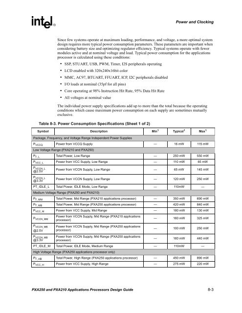
Power <strong>and</strong> Clocking<br />
Since few systems operate at maximum loading, performance, <strong>and</strong> voltage, a more optimal system<br />
design requires more typical power consumption parameters. These parameters are important when<br />
considering battery size <strong>and</strong> optimizing regulator efficiency. Typical systems operate with fewer<br />
modules active <strong>and</strong> at nominal voltage <strong>and</strong> load. Typical power consumption for the applications<br />
processor is calculated using these conditions:<br />
• SSP, STUART, USB, PWM, Timer, I2S peripherals operating<br />
• LCD enabled with 320x240x16bit color<br />
• MMC, AC97, BTUART, FFUART, ICP, I2C peripherals disabled<br />
• I/O loads at nominal (35pf for all pins)<br />
• Core operating at 98% Instruction Hit Rate, 95% Data Hit Rate<br />
• All voltages at nominal value<br />
The individual power supply specifications add up to more than the total because the operating<br />
conditions which cause maximum power consumption on each supply are sometimes mutually<br />
exclusive.<br />
Table 8-3. Power Consumption Specifications (Sheet 1 of 2)<br />
Symbol Description Min 1 Typical 1 Max 1<br />
Package, Frequency, <strong>and</strong> Voltage Range Independent Power Supplies<br />
P VCCQ Power from VCCQ Supply — 16 mW 115 mW<br />
Low Voltage Range (<strong>PXA210</strong> <strong>and</strong> <strong>PXA250</strong>)<br />
P T_L Total Power, Low Range — 250 mW 550 mW<br />
P VCC_L Power from VCC Supply, Low Range — 110 mW 65 mW<br />
P VCCN_L<br />
@2.5V<br />
P VCCN_L<br />
@3.3V<br />
Power from VCCN Supply, Low Range — 65 mW 145 mW<br />
Power from VCCN Supply, Low Range — 120 mW 250 mW<br />
PT_IDLE_L Total Power, IDLE Mode, Low Range — 110mW —<br />
Medium Voltage Range (<strong>PXA250</strong> <strong>and</strong> <strong>PXA210</strong>)<br />
P T_MM Total Power, Mid Range (<strong>PXA210</strong> applications processor) — 350 mW 690 mW<br />
P T_MB Total Power, Mid Range (<strong>PXA250</strong> applications processor) — 420 mW 840 mW<br />
P VCC_M Power from VCC Supply, Mid Range — 180 mW 130 mW<br />
P VCCN_MM<br />
P VCCN_MB<br />
@2.5V<br />
P VCCN_MB<br />
@3.3V<br />
Power from VCCN Supply, Mid Range (<strong>PXA210</strong> applications<br />
processor)<br />
Power from VCCN Supply, Mid Range (<strong>PXA250</strong> applications<br />
processor)<br />
Power from VCCN Supply, Mid Range (<strong>PXA250</strong> applications<br />
processor)<br />
— 160 mW 325 mW<br />
— 100 mW 250 mW<br />
— 160 mW 440 mW<br />
PT_IDLE_M Total Power, IDLE Mode, Medium Range — 110mW —<br />
High Voltage Range (<strong>PXA250</strong> applications processor only)<br />
P T_HB Total Power, High Range (<strong>PXA250</strong> applications processor) — 450 mW 890 mW<br />
P VCC_H Power from VCC Supply, High Range — 275 mW 220 mW<br />
<strong>PXA250</strong> <strong>and</strong> <strong>PXA210</strong> <strong>Applications</strong> <strong>Processors</strong> Design Guide 8-3


