

Intel PXA250 and PXA210 Applications Processors
Intel PXA250 and PXA210 Applications Processors
Intel PXA250 and PXA210 Applications Processors

Create successful ePaper yourself
Turn your PDF publications into a flip-book with our unique Google optimized e-Paper software.
LCD Display Controller<br />
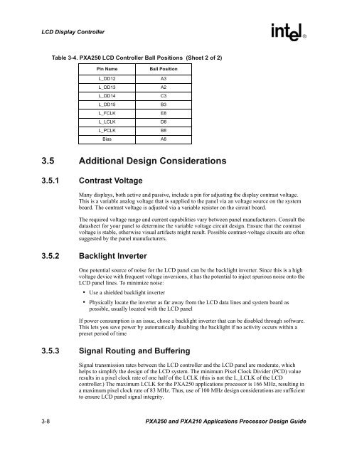
Table 3-4. <strong>PXA250</strong> LCD Controller Ball Positions (Sheet 2 of 2)<br />
Pin Name<br />
L_DD12<br />
L_DD13<br />
L_DD14<br />
L_DD15<br />
L_FCLK<br />
L_LCLK<br />
L_PCLK<br />
Bias<br />
Ball Position<br />
A3<br />
A2<br />
C3<br />
B3<br />
E8<br />
D8<br />
B8<br />
A8<br />
3.5 Additional Design Considerations<br />
3.5.1 Contrast Voltage<br />
Many displays, both active <strong>and</strong> passive, include a pin for adjusting the display contrast voltage.<br />
This is a variable analog voltage that is supplied to the panel via an voltage source on the system<br />
board. The contrast voltage is adjusted via a variable resistor on the circuit board.<br />
The required voltage range <strong>and</strong> current capabilities vary between panel manufacturers. Consult the<br />
datasheet for your panel to determine the variable voltage circuit design. Ensure that the contrast<br />
voltage is stable, otherwise visual artifacts might result. Possible contrast-voltage circuits are often<br />
suggested by the panel manufacturers.<br />
3.5.2 Backlight Inverter<br />
One potential source of noise for the LCD panel can be the backlight inverter. Since this is a high<br />
voltage device with frequent voltage inversions, it has the potential to inject spurious noise onto the<br />
LCD panel lines. To minimize noise:<br />
• Use a shielded backlight inverter<br />
• Physically locate the inverter as far away from the LCD data lines <strong>and</strong> system board as<br />
possible, usually located with the LCD panel<br />
If power consumption is an issue, chose a backlight inverter that can be disabled through software.<br />
This lets you save power by automatically disabling the backlight if no activity occurs within a<br />
preset period of time<br />
3.5.3 Signal Routing <strong>and</strong> Buffering<br />
Signal transmission rates between the LCD controller <strong>and</strong> the LCD panel are moderate, which<br />
helps to simplify the design of the LCD system. The minimum Pixel Clock Divider (PCD) value<br />
results in a pixel clock rate of one half of the LCLK (this is not the L_LCLK of the LCD<br />
controller.) The maximum LCLK for the <strong>PXA250</strong> applications processor is 166 MHz, resulting in<br />
a maximum pixel clock rate of 83 MHz. Thus, use of 100 MHz design considerations are sufficient<br />
to ensure LCD panel signal integrity.<br />
3-8 <strong>PXA250</strong> <strong>and</strong> <strong>PXA210</strong> <strong>Applications</strong> Processor Design Guide


